 | –≠–ª–µ–∫—Ç—Ä–æ–Ω–Ω—ã–π –∫–æ–º–ø–æ–Ω–µ–Ω—Ç: AME9002 | –°–∫–∞—á–∞—Ç—å:  PDF PDF  ZIP ZIP |

AME, Inc.
1
AME9002
CCFL Backlight Controller
Preliminary
l
Small package: 24 pins for QSOP/ SOIC/
PDIP packages
l
Drives multiple tubes
l
Special 1 second start up mode
l
Automatically checks for common fault
conditions
l
7.0V < Vbatt < 24V
l
Low component count
l
Low Idd < 3.5mA
l
<1uA shutdown mode
l
Battery UV lockout
l
Brightness polarity select
The AME9002 is AME's next generation direct drive
CCFL controller. Like its cousin, the AME9001, the
AME9002 controller provides a cost efficient means to
drive single or multiple cold cathode fluorescent lamps
(CCFL), driving 3 external MOSFETs that, in turn, drive a
wirewound transformer that is coupled to the CCFL.
However the AME9002 includes extra circuitry that al-
lows for a special one second start up period wherein the
voltage across the CCFL is held at a higher than normal
voltage to allow older tubes (or cold tubes) a period in
which they can "warm up". During this one second
startup period the driving frequency is adjusted off of reso-
nance so that the tube voltage can be controlled. As
soon as the CCFL "strikes" the special start up period
ends and the circuit operates in its normal mode.
The AME9002 includes features such as soft start, duty
cycle dimming control, dimming control polarity selec-
tion, undervoltage lockout and fault detection. It is de-
signed to work with input voltages from 7V up to 24V.
When disabled the circuit goes into a zero current mode.
l
Notebook computers
l
LCD/TFT displays
n
General Description
n
Features
n
Applications
n
Pin Configuration
AME9002
1. VREF
2. CE
3. SSC
4. RDELTA
5. FAULTB
6. RT2
7. VSS
8. OVPH
9. OVPL
10.FCOMP
11.CSDET
12.BATTFB
13. OUTC
14. OUTAPB
15. OUTA
16. VBATT
17. BRPOL
18. VDD
19. CT1
20. FB
21. COMP
22. BRIGHT
23. SSV
24. PNP
n
System Block Diagram
AME
9002
Controller
External
Components
CCFL Array
N
+
Resistors
+
Capacitors
LIGHT
1
2
3
4
5
6
7
8
9
10
24
23
22
21
20
19
18
17
16
15
11
12
14
13
AME9002

AME, Inc.
2
CCFL Backlight Controller
AME9002
Preliminary
n
Pin Description
Pin #
Pin Name
Pin Description
1
VREF
Reference. Compensation point for the 3.4V internal voltage reference. Must have
bypass capacitor connected here to VSS.
2
CE
Chip enable. When low (<0.4V) the chip is put into a low current (~0uA) shutdown
mode.
3
SSC
Blanking interval ramp. During the first cycle this pin sources 140nA. The first cycle
is used to define the initial start up period, often on the order of one second. During
subsequent cycles SSC sources 140
m
A. This is primarily used to provide a "blanking
interval" at the beginning of every dimming cycle to temporarily disable the fault
protection circuitry. The blanking interval is active when V(SSC) < 3.0 volts. (See
application notes.)
4
RDELTA
A resistor connected from this pin to VDD determines the amount that the voltage at
FCOMP modulates the switching frequency. The frequency is inversely proportional to
the voltage at FCOMP.
5
FAULTB
FAULTB pulls low when a fault is detected.
6
RT2
A resistor from this pin to VSS sets the minimum frequency of the VCO. The voltage at
this pin is 1.5V
7
VSS
Negative supply. Connect to system ground.
8
OVPH
Over voltage protection input (HIGH). Indirectly senses the voltage at the secondary of
the transformer through a resistor (or capacitor) divider. During the initial start up
period, if OVPH is > 3.3V, FCOMP is driven towards VSS (increasing the frequency)
and SSV is reset to zero (which decreases the duty cycle). After the initial start up
period is completed the circuit will shut down if OVPH is > 3.3V.
9
OVPL
Over voltage protection input (LOW). During the initial start up period if OVPL < 2.5
volts then FCOMP is allowed to ramp up (decreasing the oscillator frequency allowing
the circuit to get closer to resonance). If, during the initial start up period, OVPL > 2.5
volts then FCOMP is held at its original value (not allowed to increase so the
oscillator frequency stays constant). This action is designed to hold the voltage
across the CCFL constant while the CCFL "warms up".
10
FCOMP
Frequency control point. Initially this pin is at VSS which yields a maximum switching
frequency. Depending on the voltage at OVPL and OVPH the pin FCOMP will normally
ramp upwards lowering the switching frequency towards the circuit's resonant
frequency.

AME, Inc.
3
AME9002
CCFL Backlight Controller
Preliminary
n
Pin Description
Pin #
Pin Name
Pin Description
11
CSDET
Current sense detect. Connect this pin to the CCFL current sense resistor divider.
During the initial startup period this pin senses that the CCFL has struck when
V(CSDET) > 1.25 volts. If, after the initial start up period, this pin is below 1.25V for 4
consecutive clock cycles after SSC > 3V then the circuit will shutdown.
12
BATTFB
UVLO feedback pin. If this pin is above 1.5V then the OUTA pin is allowed to switch, if
below 1.25V then OUTA is disabled.
13
OUTC
Drives one of the external NFETs, opposite phase of OUTAPB.
14
OUTAPB
Drives one of the external NFETs, opposite phase of OUTC.
15
OUTA
Drives the high side PFET.
16
VBATT
Battery input. This is the positive supply for the OUTA driver.
17
BRPOL
Brightness polarity control. When this pin is low the CCFL brightness increases as
the voltage at the BRIGHT pin increases. When this pin is high the CCFL brightness
decreases as the voltage at the BRIGHT pin increases.
18
VDD
Regulated 5V supply input.
19
CT1
Sets the dimming cycle frequency. Usually about 100Hz.
20
FB
Negative input of the voltage control loop error amplifier.
21
COMP
Output of the voltage control loop error amplifier.
22
BRIGHT
Brightness control input. A DC voltage on this controls the duty cycle of the dimming
cycle. This pin is compared to a 3V ramp at the CT1 pin.
23
SSV
Soft start ramp for the voltage control loop. (20uA source current.) The voltage at SSV
clamps the voltage at COMP to be no greater than SSV thereby limiting the increase of
the switching duty cycle.
24
PNP
Drives the base of an external PNP transistor used for the 5V LDO.

AME, Inc.
4
CCFL Backlight Controller
AME9002
Preliminary
n
Ordering Information
AME9002 x x x
x x
Operating Temperature Range
Number of Pins
Package Type
Pin Configuration
Special Feature
A: 1 . VREF
E: -40
O
C to 85
O
C
J: SOIC (300 mil)
H: 24
Z: Lead free
2 . CE
P: Plastic DIP
3 . SSC
T: QSOP
4 . RDELTA
5 . FAULTB
6 . RT2
7 . VSS
8 . OVPH
9 . OVPL
10. FCOMP
11. CSDET
12. BATTFB
13. OUTC
14. OUTAPB
15. OUTA
16. VBATT
17. BRPOL
18. VDD
19. CT1
20. FB
21. COMP
22. BRIGHT
23. SSV
24. PNP
Pin Configuration
Special Feature
Operating
Temperature Range
Package Type
Number of
Pins

AME, Inc.
5
AME9002
CCFL Backlight Controller
Preliminary
n
Absolute Maximum Ratings
n
Recommended Operating Conditions
n
Thermal Information
Caution: Stress above the listed absolute maximum rating may cause permanent damage to the device
Parameter
Maximum
Unit
Battery Voltage (VBATT)
25
V
ESD Classification
B
Maximum
Unit
325
o
C / W
150
o
C
300
o
C
Thermal Resistance (QSOP - 24)
Maximum Junction Temperature
Parameter
Maximum Lead Temperature (10 Sec)
n
Ordering Information (contd.)
Parameter
Rating
Unit
Battery Voltage (VBATT)
7 - 24
V
Ambient Temperature Range
- 40 to + 85
o
C
Junction Temperature
- 40 to + 125
o
C
Part Number
Marking
Output Voltage
Package
Operating Temp. Range
AME9002AETH
AME9002AETH
xxxxxxxx
yyww
N/A
QSOP-24
- 40
o
C to + 85oC
AME9002AEPH
AME9002AEPH
xxxxxxxx
yyww
N/A
PDIP-24
- 40
o
C to + 85
o
C
AME9002AEJH
AME9002AEJH
xxxxxxxx
yyww
N/A
SOIC-24
- 40
o
C to + 85
o
C

AME, Inc.
6
CCFL Backlight Controller
AME9002
Preliminary
Parameter
Symbol
Min
Typ
Max
Units
Output voltage
V
DD
4.9
5.15
5.35
V
Line regulation
V
DDLINE
-0.5
0.5
%
Load regulation
V
DDLOAD
-0.2
0.2
%
Temperature drift
V
DDTC
0.5
%
Initial voltage
V
REF
3.25
3.4
3.525
V
Line regulation
V
REFLINE
-0.1
0.1
%
Temperature drift
V
REFTC
100
ppm/C
Ramp amplitude
V
CT1
3
V
Frequency
F
CT1
70
130
Hz
Line regulation
LINE
CT1
-1
1
%
Temperature drift
TC
CT1
=+-3
%
Comparator offset
VOS
CT1
10
mV
Initial frequency
F
VCO(OUTA)
47
52
kHz
Line regulation
LINE
VCO
-0.8
0.8
%
Temperature drift
TC
VCO
+-0.5
%
VCO pullin range
PULL
VCO
RT2/(RDELTA X 5)
%
Offset voltage, WRT Vref
V
OS
-40
40
mV
Input bias current
I
B
1
nA
Input offset current
I
OS
1
nA
Open loop gain
A
OL
70
dB
Unity gain frequency
F
T
1
Mhz
Output high voltage (comp)
V
OH
3.39
V
Output low voltage
V
OL
0.4
V
-10C < Ta < 70C
Vbatt = 15V, Iref = 0
7< Vbatt < 24V
-10C <Ta < 70C
3.4V reference (VREF)
-10C < Ta < 70C
Test Condition
Brightness oscillator (CT1, BRIGHT)
7<Vbatt<24
Vbatt=7V, 0mA < Iload < 25mA
5V supply (VSUPPLY)
7< Vbatt < 24V
RT2 = 56k
Vco oscillator (RT2, RDELTA)
7< Vbatt < 24V
-10C < Ta < 70C
Error amplifiers (FB, COMP)
I
SINK
= 500uA
I
SOURCE
= 50uA
n
Electrical Specifications
TA= 25
O
C unless otherwise noted, VBATT = 15V, CT1 = 0.047uF, RT2 = 56K

AME, Inc.
7
AME9002
CCFL Backlight Controller
Preliminary
n
Electrical Specifications(contd.)
TA= 25
O
C unless otherwise noted, VBATT = 15V, CT1=0.047uF, RT2 = 56K
Parameter
Symbol
Min
Typ
Max
Units
Peak current
I
PEAKA
1
Amp
Output Low Voltage
V
OL
10.55
V
Output High Voltage
V
OH
14.4
V
Peak current
I
PEAKBC
1
Amp
Output Low Voltage
V
OL
0.25
V
Output High Voltage
V
OH
VDD - .7
V
Initial SSC current
I
SSCINIT
100
500
nA
Normal SSC current
I
SSC
100
500
uA
SSV current
I
SSV
10
25
uA
CE high threshold
CE
HIGH
1.5
V
CE low threshold
CE
LOW
0.4
V
OVPH threshold
OVP
HI
3.2
3.55
V
OVPL threshold
OVP
LO
2.3
2.7
V
CSDET threshold
V
THCS
1.1
1.4
V
FCOMP charging current
I
FCOMP
0.8
1
1.2
uA
BATTFB high threshold
V
THBATHI
1.4
1.6
V
BATTFB low threshold
V
THBATLO
1.15
1.35
V
Average supply current
I
BATT
2.5
6
mA
Average off current
I
OFF
10
uA
Other parameters
Test Condition
-5mA
0.2mA
No FET gate current
Output A (OUTA)
Other outputs (OUTAPB, OUTC)
I
SOURCE
= 10mA
Soft start clamps (SSC, SSV)
In the application
I
SINK
= 10mA

AME, Inc.
8
CCFL Backlight Controller
AME9002
Preliminary
n
Block Diagram
1
2
3
4
5
6
7
8
9
10
11
12
3.4V
REF
5V
LDO
13
14
15
16
17
18
19
20
21
22
23
24
C
B
A
B
A
C
Fault
Logic
V
CO
2bit
Count
2
7.5V
Dimming
RAMP
CEN
REF
C2
1
µ
µ
µ
µ
CE
SSC
Logic
To Chip Enable
C3
0.039
µ
µ
µ
µ
R3
RDELTA
FAULTB
V
Supply
RT2
R2
56K
VSS
OVPH
OVPL
FCOMP
CSDET
R35
R36
D16
R10
604
R9
249
R41
10K
R40
60K
VBATT
BATTFB
C32
1
µ
µ
µ
µ
F
Q1
VBATT
R4
2K
PNP
SSV
BRIGHT
COMP
FB
CT1
VDD
BRPOL
VBATT
OUTA
OUTAPB
OUTC
C14
1000pF
BRIGHTNESS
Control VOLT.
C8
47nF
R7
30K
C4
0.047
µ
µ
µ
µ
F
C7
4.7
µ
µ
µ
µ
F
HI=Reverse
LO=Normal
C7
Q2
Q3-1
Q3-2
HS
Driver
PWM
NORM
2.5V
RES_SSV
2VOK
CE
BLANK
Later
140
µ
µ
µ
µ
A
140
nA
1
ST
RES_SSC
3V
RAMP
CLK
1.5V
3.3V
2.5V
2.5V
1
µ
µ
µ
µ
A
RES_SSC
RES_SSV
RES_FCOMP
BAITOK
RES_FCOMP
1.25V
1.5V
1.25V
CLK
EA1
STRIKE

AME, Inc.
9
AME9002
CCFL Backlight Controller
Preliminary
n
Application Schematic
Figure 2. Double Tube Application Schematic (7V < Vbatt < 24V)
1
2
3
4
5
6
7
8
9
10
11
12
13
14
15
16
17
18
19
20
21
22
23
24
VREF
CE
SSC
RDELTA
FAULTB
RT2
VSS
OVPH
OVPL
FCOMP
CSDET
BATTFB
PNP
SSV
BRIGHT
COMP
FB
CT1
VDD
BRPOL
VBATT
OUTA
OUTAPB
OUTC
R1
2K
Q1
C14
1000p
0.1
µ
µ
µ
µ
F
C8
47nF
R7
30K
C4
0.047
µ
µ
µ
µ
F
C7
4.7
µ
µ
µ
µ
F
C2
1
µ
µ
µ
µ
F
C3
0.047
µ
µ
µ
µ
F
R3
15k
V
DD
R2
40K
D17
C33
100p
D16
R36
C32
2.2nF
HI=Reverse
LO=Normal
R40
60k
R41
10k
Q3-2
Q2
T1
R10
680
R9A
221
R38
3k
R37
2meg
Q3-1
R36
3k
R35
2meg
R40
7.5k
C34
0.01u
R9B
221
VDD
R42,43
10k
R45
1M
D20
D21
D22
D23

AME, Inc.
10
CCFL Backlight Controller
AME9002
Preliminary
Overview
The AME9002 application circuit drives a CCFL (cold
cathode fluorescent lamp) with a high voltage sine wave
in order to produce an efficient and cost effective light
source. The most common application for this will be as
the backlight of either a notebook computer display, flat
panel display, or personal digital assistant (PDA).
The CCFL tubes used in these applications are usually
glass rods that can range from several cm to over 30cm
and 2.5mm to 6mm in diameter. Typically they require a
sine wave of 600V and they run at a current of several
milliamperes. However, the starting (or striking) voltage
can be as high as 2000V. At start up the tube looks like
an open circuit, after the plasma has been created the
impedance drops and current starts to flow. The starting
voltage is also known as the striking voltage because
that is the voltage at which an arc "strikes" through the
plasma. The IV characteristic of these tubes is highly
non-linear.
Traditionally the high voltage required for CCFL opera-
tion has been developed using some sort of transformer -
LC tank circuit combination driven by several small power
mosfets. The AME9002 application uses one external
PMOS, 2 external NMOS and a high turns ratio trans-
former with a centertapped primary. Lamp dimming is
achieved by turning the lamp on and off at a rate faster
than the human eye can detect, sometimes called "duty
cycle dimming". These "on-off" cycles are known as
dimming cycles. Alternate dimming schemes are also
available.
Steady State Circuit Operation
Figure 1 shows a block diagram of the AME9002.
Throughout this datasheet like components have been
given the same designations even if they are on a differ-
ent figure. The block diagram shows PMOS Q2 driving
the center tap primary of T1. The gate drive of Q2 is a
pulse width modulated (PWM) signal that controls the
current into the transformer primary and by extension,
controls the current in the CCFL. The gate drive signal of
Q2 drives all the way up to the battery voltage and down
to 7.5 volts below Vbatt so that logic level transistors
may be used without their gates being damaged. An
internal clamp prevents the Q2 gate drive (OUTA) from
driving lower than Vbatt-7.5V.
NMOS transistors Q3-1 and Q3-2 alternately connect
the outside nodes of the transformer primary to VSS.
These transistors are driven by a 50% duty cycle square
wave at one-half the frequency of the drive signal applied
to the gate of Q2.
n
Application Notes
Figure 3 illustrates some ideal gate drive waveforms for
the CCFL application. Figure 4 and 5 are detailed views
of the power section from Figures 1 and 2. Figure 5 has
the transformer parasitic elements added while Figure 4
does not. Referring to Figures 4 and 5, NMOS transis-
tors Q3-1 and Q3-2 are driven out of phase with a 50%
duty cycle signal as indicated by waveforms in Figure 3.
The frequency of the NMOS drive signals will be the fre-
quency at which the CCFL is driven. PMOS transistor,
Q2, is driven with a pulse width modulated signal (PWM)
at twice the frequency of the NMOS drive signals. In
other words, the PMOS transistor is turned on and off
once for every time each NMOS transistor is on. In this
case, when NMOS transistor Q3-1 and PMOS transistor
Q2 are both on then NMOS transistor Q3-2 is off, the
side of the primary coil connected to NMOS transistor
Q3-1 is driven to ground and the centertap of the trans-
former primary is driven to the battery voltage. The other
side of the primary coil connected to NMOS transistor
Q3-2 (now "off") is driven to twice the battery voltage
(because each winding of the primary has an equal num-
ber of turns).
Current ramps up in the side of the primary connected
to Q3-1 (the "on" transistor), transferring power to the
secondary coil of transformer. The energy transferred from
the primary excites the tank circuit formed by the trans-
former leakage inductance and parasitic capacitances that
exist at the transformer secondary. The parasitic capaci-
tances come from the capacitance of the transformer sec-
ondary itself, wiring capacitances, as well as the parasitic
capacitance of the CCFL. Some applications may actu-
ally add a small amount of parallel capacitance (~10pF)
on the output of the transformer in order to dominate the
parasitic capacitive elements.
When the PMOS, Q2, is turned off, the voltage of the
transformer centertap returns to ground as does the drain
of NMOS transistor Q3-2 (the drain of Q3-2 was at twice
the battery voltage). Halfway through one cycle, NMOS
transistor Q3-1 (that was on) turns off and NMOS transis-
tor Q3-2 (that was off) turns on. At this point, PMOS
transistor Q2 turns on again, allowing current to ramp up
in the side of the primary that previously had no current.
Energy in the primary winding is transferred to the sec-
ondary winding and stored again in the leakage induc-
tance L
leak
, but this time with the opposite polarity. The
current alternately goes through one primary winding then
the other.
The duty cycle of PMOS transistor Q2 controls the
amount of power transferred from the primary winding to
the secondary winding in the transformer. Note that the
CCFL circuit can work with PMOS transistor Q2 on con-

AME, Inc.
11
AME9002
CCFL Backlight Controller
Preliminary
Figure 3. Idealized Gate Drive Waveforms
Figure 5.
Power Stage Single Tube Components
with parasitic elements
(Same component designations used throughout)
Figure 4.
Power Stage Single Tube Components
(Same component designations used throughout)
Signals OUTC
and OUTAPB
are the inverse
of each other.
V
BATT
R9+R10
To Control
Circuitry
Q3-1
T1
Q2
Q3-2
CCFL
OUTC
D=50%
Vhi = 5V
Vlo = 0V
F = fosc/2
OUTA
D = 0-100%
Vhi = Vbatt
Vlo = Vbatt-7.5V
F = fosc
OUTAPB
D=50%
Vhi = 5V
Vlo = 0V
F = fosc/2
D4
D5
To Control
Circuitry
Lleak
L p
L p
1:N
Q2
OUTA
D = 0-100%
Vhi = Vbatt
Vlo = Vbatt-7.5V
F = fosc
Q3-1
Q3-2
CCFL
T1
D5
D4
OUTAPB
D=50%
Vhi = 5V
Vlo = 0V
F = fosc/2
OUTC
D=50%
Vhi = 5V
Vlo = 0V
F = fosc/2
Signals OUTC
and OUTAPB
are the inverse
of each other.
C
parasitic
V
BATT
R9+R10
V
BATT
5V
0V
5V
0V
V
BATT
- 7.5V
Q2 Gate
Q3-1 Gate
Q3-2 Gate
(OUTA)
(OUTAPB)
(OUTC)

AME, Inc.
12
CCFL Backlight Controller
AME9002
Preliminary
stantly (i.e. a duty cycle of 100%), although the power
would be unregulated in this case.
Figures 6,7 illustrates various oscilloscope waveforms
generated by the CCFL circuit in operation. These fig-
ures show that the duty cycle of the gate drive at Q2
decreases as the battery voltage increases from 9 V to
21 V (as one would expect in order to maintain the same
output power).
The first three traces in Figures 6 and 7 show the gate
drive waveforms for transistors Q2, Q3-1, and Q3-2, re-
spectively. As mentioned before, the gate drive wave-
form for transistor Q2 drives up to the battery voltage but
down only to approximately 7.5 V below the battery volt-
age. The fourth trace (in Figures 6,7) shows the voltage
at centertap of the primary winding (it is also the drain of
PMOS transistor, Q2). This waveform is essentially a
ground to a battery voltage pulse of varying duty cycle.
When the centertap of the primary is driven high, current
increases through PMOS transistor, Q2 as indicated by
the sixth trace down from the top. In region I the drain
current of Q2 is equal and opposite to the drain current of
Q3-1 since the gate of Q3-1 is high and Q3-1 is on. In
region III the drain current of Q2 will be equal and oppo-
site to the drain current of Q3-2 (not shown). In region II
when PMOS transistor Q2 is switched off, the current
through this transistor, after an initial sharp drop, ramps
back down towards zero.
In Figures 6 and 7 the fifth trace down from the top
shows the drain voltage of Q3-1. (The trace for NMOS
transistor Q3-2, not shown, would be identical, but shifted
in time by half a period.) The seventh trace down from
the top shows the current through the NMOS transistor
Q3-1, which is equal to the current in PMOS transistor
Q2 for the portion of time that PMOS transistor Q2 is
conducting (see region I, for example). As the current
ramps up in the primary winding, energy is transferred to
the secondary winding and stored in the leakage induc-
tance L
leak
(and any parasitic capacitance on the second-
ary winding). If the current in the NMOS transistor is
close to zero when that NMOS transistor is turned off
that means that the CCFL circuit is being driven close to
its resonant frequency. If the circuit is being driven too
far from its resonant point then there will be large residual
currents in the transistors when they are turned off caus-
ing large ringing, lower efficiency and more stress on the
components. So called "soft switching" is achieved when
the MOS drain current is zero while the MOS is being
turned off. The driving frequency and transformer param-
eters should be chosen so that soft switching occurs.
Once PMOS transistor Q2 completes one on/off cycle,
it is repeated again with the alternate NMOS transistor
conducting. This complementary operation produces a
symmetric, approximately sinusoidal waveform at the in-
put to the CCFL load, as shown by the bottom trace in
Figures 6 and 7.
The operation of the CCFL circuit can be divided into 4
regions (I, II, III, and IV) as shown in Figures 6 and 7.
Figure 8-1 shows the equivalent transformer and load cir-
cuit model for region I. During region I, one of the pri-
mary windings is connected across the battery, the cur-
rent in that winding increases and energy is coupled
across to the secondary. No current flows in the other
winding because its NMOS is turned off and its body
diode is reverse biased. The drain of that NMOS stays
at twice the battery voltage because both primary wind-
ings have the same number of turns and the battery volt-
age is forced across the other primary winding.
Figure 8-2 shows the equivalent transformer and load
circuit model for region II. During region II, the battery is
disconnected from the primary winding. In this configu-
ration, current flows through both of the primary wind-
ings. The current decreases very quickly at first then
ramps down to zero at a rate that is slower than the
current ramped up. The initial drop is due to the almost
instantaneous change in inductance when current flow
shifts from one portion of the primary winding to both
portions of the primary.
Figure 8-3 shows the equivalent transformer and load
circuit model for region III. During region III, the primary
winding opposite from the one used in region I is con-
nected across the battery, increasing current in that pri-
mary winding but in a direction opposite to that of region
I. Energy is coupled across to the secondary as in re-
gion I but with opposite polarity. No current flows in the
undriven winding because its NMOS is turned off and its
body diode is reverse biased. The drain of that NMOS
stays at twice the battery voltage because both primary
windings have the same number of turns and the battery
voltage is forced on the other primary. Region III is, ef-
fectively, the inverse of region I.
Figure 8-4 shows the equivalent transformer and load
circuit model for region IV. During region IV, the battery
is disconnected from the primary winding. In this con-
figuration, current flows through both of the primary wind-
ings with opposite polarity to that in region II. The cur-
rent decreases very quickly at first then ramps down to
zero at a rate that is slower than the current ramped up.
Once again, the initial drop is due to the effective change
in inductance when current flow shifts from one portion of
the primary winding to both portions of the primary. Re-
gion IV is effectively the inverse of region II.

AME, Inc.
13
AME9002
CCFL Backlight Controller
Preliminary
Figure 7. Typical Waveforms V
BATT
=21V
Figure 6. Typical Waveforms V
BATT
=9V
Region
I
Region
II
Region
III
Region
IV
Q2 Gate
Q3-1 Gate
Q3-2 Gate
Center tap
Q3-1 Drain
I
DQ2
I
DQ3-1
I
LAMP
V
BATT
=9V
1.5V
5V
0V
5V
0V
V
BATT
0V
V
BATT
x 2
0
0
I
MAX
0
I
MAX
(OUTA)
(OUTAPB)
(OUTC)
(Q2 DRAIN)
Q3-1 Gate
Q3-2 Gate
Q3-1 Drain
Region
I
Region
II
Region
III
Region
IV
Q2 Gate
I
DQ2
I
DQ3-1
I
LAMP
13.5V
0V
2 x V
BATT
0V
0A
I
MAX
0A
I
MAX
5V
0V
5V
(OUTAPB)
(OUTC)
Center tap
V
BATT
0V
(Q2 DRAIN)
V
BATT
=21V
(OUTA)

AME, Inc.
14
CCFL Backlight Controller
AME9002
Preliminary
Figure 8-1. Region I
Figure 8-2. Region II
Figure 8-3. Region III
Figure 8-4. Region IV
Figure 9. Steady State Dimming Waveforms (after initial start up period)
Load
I
LEAK
I
C
parasitic
Load
I
C
parasitic
I
LEAK
Load
I
C
parasitic
I
LEAK
Load
I
LEAK
I
C
parasitic
"Unblanked" Faults
OVPH > 3.3V
BRIGHT
CT1
5V
SSV
OV
Ignore
Respond
Ignore
Respond
Always Respond to Over voltage Faults
~
6ms
5V
SSC
OV
"Blanked" Faults
CSDET < 1.25V
OVPL > 2.5V
Tube Current
(time not
to scale)
0.5V
3V
3V
3V

AME, Inc.
15
AME9002
CCFL Backlight Controller
Preliminary
Driving the CCFL
Unlike modified Royer schemes for driving CCFLs the
secondary winding of the AME9002 method is not de-
signed to look like a voltage source to the CCFL lamp.
The circuit acts more like a current source (or a power
source). The voltage at the transformer secondary is pri-
marily determined by the operating point of the CCFL.
The circuit will increase the duty cycle of Q2 thereby
dumping more and more energy across to the secondary
tank circuit until the CCFL tube current achieves regula-
tion or one of the various fault conditions is met.
There are two major modes of operation of the AME9002.
The start up mode consists of the time from intial power
up until the tube strikes or 1 second elapses. The steady
state mode consists of operation that occurs after the
start up mode finishes.
The start up mode is useful for coaxing old or cold
tubes into striking. It is believed that as a tube ages it
becomes more and more difficult to strike an arc through
the gas. Cold temperatures make this problem even
worse. The AME9002 will allow higher than normal oper-
ating voltages across the CCFL for a period of up to one
second in order to facilitate strking. This feature should
extend the usable life of the CCFL as well as simplifying
start up for "problem" applications.
Start Up Mode
When the circuit is first powered up or the CE pin tran-
sitions from a low to a high state a special mode of op-
eration, known as the "start up mode", is initiated that
will last for a maximum of one second. The exact dura-
tion of the start up period is determined by capacitor C3
on the SSC pin. Figure 10 shows a flow chart of the CCFL
ignition sequence described here. The start up mode
will end when one of two conditions is met:
a) The CCFL strikes and the current sense voltage at
the CSDET pin rises above 1.25V.
b) The one second time period ends without the tube
being struck, in this case the circuit will shut down.
On the first cycle after power on (or a low to high tran-
sition on CE) C3 is initially discharged and the voltage on
SSC is zero. It is charged up by a 140nA current source.
When the voltage on C3 reaches 3 volts the start up mode
has ended. A value of 0.39uF for C3 nominally yields a
one second start up period. If the one second time period
ends before the CCFL strikes then the circuit is shut-
down until the user toggles the power supply or CE tran-
sitions from low to high again. In other words, if the CCFL
successfully starts up then the start up time period will
end before the one second time period is up.
The SSC pin and C3 are also used to set the blanking
period during steady state operation. This operation is
described more completely below.
At the beginning of the start up period capacitor C32,
connected to FCOMP, is also discharged and the voltage
at FCOMP is zero. The voltage at FCOMP controls the
frequency at which the FETs are driven. When FCOMP
is zero the frequency is at its maximum value. When
FCOMP reaches 5V then the switching frequency is at
its minimum value. The exact relation between the volt-
age at FCOMP and oscillator frequency is described more
fully in the detailed description of the oscillator circuitry.
At the beginning of start up mode FCOMP is zero volts
so the switching frequency is at its maximum value. It is
intended that this maximum frequency is significantly
above the resonant frequency of the tank circuit made up
of the transformer and CCFL load. In this way the voltage
at the CCFL is lower than would be expected if the circuit
was driven nearer to its resonant frequency. At this point
in the operation of the circuit we assume that the CCFL
has not struck and therefore appears as an open circuit to
the transformer. After the tube has struck the voltage at
the transformer output is controlled by the IV relationship
of the CCFL. Without the variable frequency drive avail-
able with the AME9002 the user is unable to control the
voltage across the CCFL before the CCFL strikes and
current starts flowing in the CCFL.
Capacitor C32 is charged by a 1uA current source with
the following conditions:
a) If OVPL < 2.5V the charging current is 1uA and
the voltage at FCOMP ramps positive.
b) If OVPL > 2.5V and OVPH < 3.3V then the charg-
ing current is zero and the voltage at FCOMP re-
mains the same.
c) If OVPH > 3.3V then FCOMP is discharged to
approximately 1V, SSV is also driven to VSS.
These conditions allow the voltage across the CCFL to
be controlled during the start up period. The two thresh-
olds available at OVPL and OVPH allow the user to tailor
the start behavior for particular tubes.
In Figure 11, initially SSV=SSC=FCOMP= zero
volts. The switching duty cycle is zero, the switching
frequency is maximum and the one second time period
ramp has just started. The SSV ramps positive which

AME, Inc.
16
CCFL Backlight Controller
AME9002
Preliminary
Figure 10. Ignition Flow Chart
START
F=Fmax
Set SSV = 0V
F(new)=F(old) - delta
F > Fmin?
V(OVPL) > 2.5V
Yes
Start 1 second
timer
No
Timer
End?
V(OVPH)>
3.3V
Shutdown
V(CSDET) <
1.25V
Timer
End?
No
V(OVPL) > 2.5V
V(CSDET) < 1.25V
(after normal blanking
and for 4 clk cycles)
F(new)=F(old) - delta
F > Fmin?
Yes
No
No
No
Start Up Side -------
|
------ Steady State
Operation Side
Yes
Yes
Yes
Yes
Yes
No
No
Yes
No
No
Yes

AME, Inc.
17
AME9002
CCFL Backlight Controller
Preliminary
Figure 11. Start Up and Steady State Waveform
SSC
F
COMP
SSV
VBATTOK
VDDOK
}
VALID
<3V
<1 Sec
OVPH>3.3V
F = f
MIN
< Initial Start Up Period>
<Two full scale brightness cycles after strike>
<After CCFL strikes>
BLANK
BLANK
3V
F = f
MIN
~ 6mS
<Steady state op. with duty cycle dimming>
BRIGHT *
5V
CT1
CSDET
F
COMP
ramps up
Frequency decreases
F
COMP
constant
Frequency constant
OVPH>3.3V
F
COMP
= V
Frequency = F
MAX
SSV=0V
COMP=0V
OVPL<2.5V
OVPH<3.3V
OVPL>2.5V
OVPH < 3.3V
IF:
THEN:
Tube has struck and initial
start period has ended.
CSDET > 1.25V
OVPH > 3.3V
OVPL > 2.5V
CSDET < 1.25V for
4 consecutive clock cycles
Immediate shutdown
during blanking period: nothing
after blanking period: shutdown
* BRPOL is Low
IF:
THEN:
during blanking period: nothing
after blanking period: shutdown
** Time axis is not to scale
OVPL<2.5V
OVPH<3.3V
OVPL>2.5V
OVPH < 3.3V
OVPL
<2.5V
OVPL>2.5V
OVPH < 3.3V
OVPL<2.5V
OVPH<3.3V
**
1.25V

AME, Inc.
18
CCFL Backlight Controller
AME9002
Preliminary
allows the switching duty cycle to increase which, in turn,
increases the voltage across the CCFL.
At some point later SSV=5 volts, SSC and FCOMP
are still ramping up. The tube voltage continues to in-
crease, the switching duty cycle is no longer limited by
SSV and is able to go to 100%, if indicated by the error
amp loop. The switching frequency continues to decrease
forcing the tube voltage higher. If the CCFL voltage is
high enough so that OVPL > 2.5V (OVPL senses the
CCFL voltage through a resistor or capacitor divider) then
FCOMP stops increasing and the frequency remains con-
stant. The frequency will remain constant until:
OVPL < 2.5V
OR....
OVPH > 3.3V (see below)
OR......
The one second time period runs out and the
circuit shuts down.
If the voltage across the tube increases enough so that
OVPH > 3.3V (as sensed through a resistor or capacitor
divider) then FCOMP is pulled low (~1V), the switching
frequency is increased, SSV is pulled low and the switch-
ing duty cycle goes to zero. It will remain in this state
until:
OVPH < 3.3V
OR....
The one second time period runs out and the circuit
shuts down.
Ideally, during one of these states, the CCFL will strike,
current will flow in the CCFL and the circuit will move
from the start up mode into the steady state mode. Once
an arc has struck, as sensed by CSDET > 1.25 volts,
then the circuit will drive the CCFL at 100% brightness
for approximately two dimming cycles (dimming cycles
are on the order of 6mS as determined by the capacitor
on CT1) in order to ensure that the CCFL is really "on".
After those two full brightness dimming cycles the nor-
mal duty brightness control takes over, alternately turn-
ing the CCFL on and off at a duty cycle determined by
the voltage at the BRIGHT pin.
Remember, the circuit will only "try" to turn on for one
second, after that point it gives up and shuts down.
Steady State Mode
At the beginning of each dimming cycle (after the start
up mode) there is initially no arc struck in the CCFL. The
CCFL load looks like an open circuit. (However an arc
has been struck successfully in the start up mode so we
assume the gas has "warmed up" and is ready to strike
an arc again.) SSV is pulled to zero volts then ramps to 5
volts allowing the duty cycle of the switches to slowly
increase to its steady state value. The voltage across
the CCFL will increase with each successive clock cycle.
Two events may then happen:
1) The gas inside the CCFL will ionize, the voltage across
the CCFL will drop, the current through the CCFL will
increase, and a stable steady state operating point
will be reached.
OR....
2) One of the three fault conditions will be met that shut
down the circuit (see Figure 11):
a) The CCFL tube voltage continues to rise until the
OVPH pin is higher than 3.3V at which point the
circuit will shut down (immediately).
b) The CCFL tube voltage continues to rise until the
OVPL pin is higher than 2.5V at which point the
circuit will shut down (except during the blanking
interval).
c) The CCFL current fails to rise high enough to keep
the undercurrent threshold at the CSDET pin from
tripping (for 4 consecutive clock cycles).
Note that condition a) can be met at any time while the
AME9002 is in steady state operation (after the start up
mode). Condition b) can only be met after the SSC pin
has risen above 3V (after blanking interval). Condition c)
can only be met after the SSC pin has crossed 3V (after
blanking interval) AND four successive undercurrent events
occur in a row (CSDET < 1.25V).
The SSC pin is pulled to VSS everytime the lamp is
turned off, whether for a dimming cycle, user shutdown
or fault occurrence. It ramps up slowly depending on the
size of capacitor C3 connected to the SSC pin. The pe-
riod of time when the b) and c) fault checks are disabled
is called the "blanking" time. The blanking time occurs
from the time SSC is pulled to VSS until it reaches 3V.
See Figure 9 for some idealized waveforms illustrating
the behavior just described.
Control Algorithm
There are 2 major control blocks (loops) within the IC.
The first loop controls the duty cycle of the driving wave-
form. It senses the CCFL current (Figure 1 or 2, resistor
R9 and R10) rectifies it, integrates it against an internal

AME, Inc.
19
AME9002
CCFL Backlight Controller
Preliminary
reference and adjusts the duty cycle to obtain the de-
sired power. This loop uses error amplifier EA1 whose
negative input is pin FB and whose output is COMP. The
positive input of EA1 is connected to a 2.5V reference.
External components, R7 and C8, set the time constant
of the integrator, EA1. In order to slow the response of
the integrator increase the value of the product:
(R7 X C8).
The second control block adjusts the brightness by
turning the lamp on and off at varying duty cycles. Each
time the lamp turns on and off is referred to as a "dim-
ming cycle". At the end of each dimming cycle the SSV
pin is pulled low, this forces COMP low as well due to the
clamping action of Clamp1 shown in Figure 1. At the
beginning of a new dimming cycle COMP tries to increase
quickly but it is clamped to the voltage at the SSV(soft-
start voltage) pin. A capacitor on the SSV pin (C8, Figure
1), which is discharged at the end of every dimming cycle,
sets the slew rate of the voltage at the SSV pin, and
hence also the maximum positive slew rate of the COMP
pin. ["Dimming cycle" is explained more fully below]
The BRIGHT, CT1 and BRPOL pins
A user-provided voltage at the BRIGHT pin is compared
with the ramp voltage at the CT1 pin (See Figure 12). If
BRPOL is tied to VSS then as the voltage at BRIGHT
increases the duty cycle of the dimming cycle and the
brightness of the CCFL increase. If BRPOL is tied to
VDD then the brightness of the CCFL diminishes as the
BRIGHT voltage increases. The frequency of the dim-
ming cycles is set by the value of the capacitor at pin
CT1 (C4 in Figure 1 and 2) and it is also proportional to
the current set by resistor R2. Setting C4 equal to
0.047uF and R2 equal to 47.5k yields a dimming cycle
frequency of approximately 125Hz. The frequency should
vary inversely with the value of C4 according to the rela-
tion:
Frequency(Hz) = 1/[4 X R2 X C4]
The
brightness may also be controlled by using a vari-
able resistor in place of R10 (See Figure 13). In this case
the BRIGHT pin should be pulled to VDD so that the CCFL
remains on constantly. This method can lead to flicker at
low intensities but it is easy to implement. Harmonic
distortion may also increase since the duty cycle of the
waveform at the gate of Q2 will vary greatly with bright-
ness. When using burst brightness control the duty cycle
of the driving waveforms should not vary because the
CCFL is running at 100% power or it is turned off. As
long as the battery voltage does not change the duty cycle
of the driving waveform also does not change greatly. This
means that harmonic distortion can be minimized by op-
timizing the frequency and transformer characteristics for
a particular duty cycle rather than a large range of duty
cycle.

AME, Inc.
20
CCFL Backlight Controller
AME9002
Preliminary
Figure 13. Alternative Brightness Control
Figure 12. Duty Cycle Dimming
BRIGHT
CT1
+
-
3V
+
-
50mV
S
R
Q
+
-
CHOP
CHOP causes the CCFL
to turn on and off
periodically.
C4
Brightness
control
voltage
Inside Chip
Outside Chip
BRPOL
5V
R
1
R
2
R
2R
BRIGHT
CT
COMP
FB
CSDET
RF
+
-
1.25V
Inside Chip
Outside Chip
This method disables
duty cycle dimming
Maximum current=
K
R
1
//(2R+R)
Minimum current=
K
(R
1
+R
2
)//(2R+R)
2.5V
T1
+
-
CHOP
+
-
Always Hi
To PWM
Comparator
To Fault
Control Logic
BRPOL
EA1
R-C-D
optional
network

AME, Inc.
21
AME9002
CCFL Backlight Controller
Preliminary
RT2, RDELTA pin
The frequency of the drive signal at the gate of Q2 is
determined by the VCO shown in Figure1. A detail of the
VCO is shown in Figure 14. The user sets the minimum
oscillator frequency with the resistor connected to pin
RT2 (R2 in the figures). The relation is:
Frequency (Hz) = 2.8E9 / R2 (ohms)
You can see from the formula that as R2 is increased
the frequency gets smaller.
Resistor R3 controls how much the oscillator frequency
increases as a function of the voltage at FCOMP. The
relationship is:
Delta frequency (Hz) = 3.44E8 * (5 - V(FCOMP)) / R3
You can see from the formula that the frequency will
decrease as the FCOMP voltage increases. The amount
of this increase is set by R3. The current in R3 decreases
as the voltage at FCOMP increases and hence decreases
the charging current into the timing capacitor of Figure
14 thereby decreasing the oscillator frequency.
Supply voltage pins, VDD and PNP
Most of the circuitry of the AME9002 works at 5V with
the exception of one output driver. That driver (OUTA)
and its power pad (VBATT) must operate up to 24V al-
though the OUTA pad may never be forced lower than 8
volts away from the VBATT pin. The OUTA pin is inter-
nally clamped to approximately 7.5 volts below the Vbatt
pin.
The AME9002 uses an external PNP device to provide
a regulated 5V supply from the battery voltage (See Fig-
ure 15). The battery voltage can range from 7V< VBATT <
24V. The PNP pin drives the base of the external PNP
device, Q1. The VDD pin is the 5V supply into the chip.
A 4.7uF capacitor, C7, bypasses the 5V supply to ground.
If an external 5V supply is available then the external
PNP would not be necessary and the PNP pin should
float.
When the CE pin is low (<0.4V) the chip goes into a
zero current state. The chip puts the PNP pin into a high
impedance state which shuts off Q1 and lets the 5V sup-
ply collapse to zero volts. When low, the CE pin also
immediately turns PMOS transistor Q2 off, however tran-
sistors Q3-1 and Q3-2 will continue to switch until the 5V
has collapsed to 3.5V. By allowing the Q3 transistors to
continue to switch for some time after Q2 is turned off
the energy in the tank circuit is dissipated gradually with-
out any large voltage spikes.
The VDD voltage is sensed internally so that the switch-
ing circuitry will not turn on unless the VDD voltage is
larger than 4.5V and the internal reference is valid. Once
the 4.5V threshold has been reached the switching cir-
cuitry will run until VDD is less than 3.5V (as mentioned
before).
Output drivers (OUTA, OUTAPB, OUTC)
The OUTAPB and OUTC pins are standard 5V CMOS
driver outputs (with some added circuitry to prevent shoot
through current). The OUTA driver is quite different (See
Figure 16). The OUTA driver pulls up to VBATT (max
24V) and pulls down to about 7.5 volts below VBATT. It is
internally clamped to within 7.5V of VBATT. On each
transition the OUTA pad will sink/source about 500mA for
100nS. After the initial 100ns burst of current the current
is scaled back to 1mA(sinking) and 12mA(sourcing). This
technique allows for fast edge transitions yet low overall
power dissipation.
Fault Protection, the OVPH, OVPL and CSDET pins
During the startup mode the AME9002 does not actu-
ally sense for fault conditions, instead it uses the volt-
ages at OVPL and OVPH to adjust the operating fre-
quency for a smooth start up. The startup itself (or
"strike") is detected when the voltage at CSDET rises
above 1.25V. There are no voltages at OVPL, OVPH or
CSDET that can cause a fault during the start up mode.
During steady state operation the AME9002 checks
for 3 different fault conditions. There are two overvoltage
conditions and one undercurrent condition that can cause
a fault. When any one of the fault conditions is met then
the circuit is latched off. Only a power on reset or tog-
gling the CE pin will restore the circuit to normal opera-
tion. (See Figure 17 for a schematic of the FAULT cir-
cuitry.)
The first fault condition check can be used to detect
overvoltages at the CCFL. Specifically, if the OVPH pin
is above 3V then this fault condition is detected. The
first fault condition is always enabled, there is no blank-
ing period (except, of course, during the start up period
when fault detection is disabled).
The second fault condition checks that the voltage at
OVPL is below 2.5V. This protection is disabled while
the SSC ramp is below 3V such as during the beginning
of every dimming cycle. Again, this check is disabled
during the start up period like all the fault checks.

AME, Inc.
22
CCFL Backlight Controller
AME9002
Preliminary
In order to enable the first two fault condition checks
then the OVP pin must, indirectly, sense the high volt-
age at the input of the CCFL. The actual CCFL voltage
must be reduced by using either a resistor or capacitor
divider such that in normal operation the voltage at OVPL
is lower than 2.5V and the voltage at OVPH is lower than
3.3V.
The third fault condition check can be used to monitor
the CCFL current. Specifically, it checks whether the
voltage at the CSDET pin is higher than 1.25V. If CSDET
does not cross its 1.25V threshold once during 4 suc-
cessive clock cycles then this fault will be triggered. This
protection is disabled while the SSC ramp is below 3V,
such as at the beginning of every dimming cycle. This
fault check is disabled during the start up mode, as are
all the fault checks. This fault condition is used to check
that a reasonable minimum amount of current is flowing
in the tube.
Figure 17 is a simplified schematic of the fault protec-
tion circuitry used in the AME9002. Most of the signals
have been previously defined however some need a little
explanation. The VDDOK signal is a power OK signal
that goes high when the 5V supply (VDD) is valid. The
CHOP signal stops the operation of the switching cir-
cuitry once every dimming cycle for burst mode bright-
ness control. The output signal, FIRST, is high during
the start up mode then is low during subsequent cycles.
It causes the SSC pin to initially source 1000 times less
current than on subsequent dimming cycles in order to
provide the 1 second initial start up period. The NORM
signal is an enable signal to the switching circuitry. When
it is high the circuit works normally. When it is low the
switching circuitry stops.
SSC and SSV pins
Besides defining the initial 1 second start up period
the SSC pin's primary role is to define a time period in
which the 2nd and 3rd fault condition (previously de-
scribed) are disabled. This period of time is called the
blanking interval. During the initial start up period after a
power on reset or just after a low to high transition on the
CE pin the SSC pin sources 140nA into an external ca-
pacitor, C3. For subsequent dimming cycles the SSC
pin sources 140uA. During steady state operation the
blanking interval is defined as the time during which
V(SSC) < 3V. Once the voltage at SSC crosses 3V the
blanking interval is finished and all three fault condition
checks are enabled. (The OVPH > 3.3V fault check is
always enabled after the initial start up period.) At the
beginning of the next dimming cycle the SSC pin is pulled
to VSS then allowed to ramp upwards again.
During steady state operation the SSV pin (like the
SSC pin) is pulled to ground at the beginning of every
dimming cycle then sources 20uA into an external ca-
pacitor. This creates a 0 to 5 volt ramp at the SSV pin.
This ramp is used to limit the duty cycle of the PWM
gate drive signal available at the OUTA pin. The SSV pin
accomplishes duty cycle limiting by clamping the COMP
voltage to no higher than the SSV voltage. Because the
magnitude of the COMP voltage is proportional to the
duty cycle of the PWM signal at OUTA the duty cycle
starts each dimming cycle at zero and slowly increases
to its steady state value as the voltage at SSV increases.
(Figure 9 shows this operation.)
During the initial start up mode the SSV pin starts at
zero volts and ramps up to 5V just as in steady state
operation. However, during the start up mode, if OVPH >
3.3V then SSV is pulled to VSS and only allowed to ramp
up when OVPH < 3.3V. This action sets the duty cycle
back to 0 volts then allows the duty cycle to increase as
the SSV voltage increases.
This type of duty cycle limiting is commonly called
"soft-start" operation. Soft start operation lessens over-
shoot on start up because the power increases gradually
rather than immediately.
Unlike the SSC pin the current sourced by the SSV pin
remains approximately 20uA during ALL dimming cycles.
BATTFB
The BATTFB pin is designed to sense the battery volt-
age and enable the pin OUTA. When the voltage at
BATTFB is below 1.25 volts then OUTA is disabled, when
the voltage at BATTFB is larger than 1.5V then OUTA is
enabled. There is 250mV of hysteresis between the turn
on and the turnoff thresholds. This pin does not disable
any other portion of the circuit except the OUTA pin.
Notably, the other two drivers, OUTAPB and OUTC con-
tinue to switch when the voltage at BATTFB is below
1.25V.
Ringing
Due to the leakage inductances of transformer T1 volt-
ages at the drains of Q3 can potentially ring to values
substantially higher than the ideal value (which is twice
the battery voltage). The application schematic in Figure
17 uses a snubbing circuit to limit the extent of the ring-
ing voltage. Components C9,R8,D2 and D3 make up the

AME, Inc.
23
AME9002
CCFL Backlight Controller
Preliminary
snubbing circuit. The nominal voltage at the common
node is approximately twice the battery voltage. If either
of the drains of Q3 ring above that voltage then diodes D2
or D3 forward bias and allow the ringing energy to charge
capacitor C9. Resistor R8 bleeds off the extra ringing
energy preventing the voltage at the common node from
increasing substantially higher than twice the battery volt-
age. The extra power dissipation is:
P(dissipated) = Vbatt
2
/ R8
For the example, in Figure 17, the power dissipation of
the snubber circuit with Vbatt=15V is 58mW or approxi-
mately 1% of the total input power. The value of R8 can
be optimized for a particular application in order to mini-
mize dissipated power.
Excessive ringing is usually a sign that the driving fre-
quency is not well matched to the resonant characteris-
tics of the tank circuit. In a well designed application a
snubber circuit will not be necessary.
Layout Considerations
Due to the switching nature of this circuit and the high
voltages that it produces this application can be sensitive
to board parasitics. In fact, one of the advantages, of this
design is that the circuit uses the parasitic elements of
the application as resonant components, thus eliminat-
ing the need for more added components.
Particular care must be taken with the different gounding
loops. The best performance has been obtained by us-
ing a "star" ground technique. The star technique re-
turns all significant ground paths back to the center of
the "star". Ideally we would place the center of the star
directly on the VSS pin of the AME9002. The bypass
capacitors would, ideally, be connected as close to the
center of the star as possible. The schematic in Figure
18 attemps to show this star ground configuration by bring-
ing all the ground returns back to the same point on the
drawing. Separate ground returns back to the star are
especially important for higher current switching paths.

AME, Inc.
24
CCFL Backlight Controller
AME9002
Preliminary
1.5V
VSS
3.0V
I_in
0
I_out
0
50:1
curent
divider
CLK
RAMP
+
-
+
-
Vco_Control
RT2
Inside chip
Outside chip
2.5V
FCOMP
OVPL
RDELTA
R3
R2
1
µ
µ
µ
µ
F
C32
3.3V
OVPH
1
µ
µ
µ
µ
A
V
DD
SSV
VDD
1
-
2
+
-
Start
UP
Inside Chip
Outside Chip
PNP
VDD
CE
V
DDOK
EN
2.5V
4.7
µ
µ
µ
µ
F
27 < V
BATT
< 24
V
BATT
R4
Q1
To Fault
Logic
C7
To user
enable circuitry
Figure 14. VCO Detail
Figure 15. LDO Detail

AME, Inc.
25
AME9002
CCFL Backlight Controller
Preliminary
Figure 16. OUTA Driver Circuitry
PWM
SIGNAL
External
PMOS, Q2
OUTA
Vbatt
100nS
100nS
1mA
Inside Chip
Outside Chip
BV=7.5V
BV=4V
BV=5V

AME, Inc.
26
CCFL Backlight Controller
AME9002
Preliminary
Figure 17. Fault Logic
+
-
1.25V
L1
CE
V
DD
+
-
+
-
2.5V
+
-
3.0V
+
-
BRIGHT
Q
RES
2Bit
Counter
Q
S
R
Q
S
R
Q
RES
2 Bit
Shift
D
Dimming
Oscillator
EN
Q
S
R
VDDOK
POR
FAULTB
NORM
SSV
FIRST
VDD
VDDOK
1.25V
BATTFB
CSDET
OVPL
SSC
+
-
3.3V
OVPH
BLNK
L3
CT1
C4
BRPOL
FCOMP
CHOPIN
CHO
P
O
UT
BLK_CS
L2
CLK

AME, Inc.
27
AME9002
CCFL Backlight Controller
Preliminary
Application Component Description
Figure 18 shows one typical application circuit for driv-
ing 4 tubes. Similar component designations are used
on similar components both in figure 2 and Figure 18 as
well as throughout this application note.
R1 - Weak pull up for the chip enable (CE) pin. The
voltage at CE will normally rise to 5 volts for a 12V
supply. Pull down on the CE node to disable the chip
and put it into a zero Idd mode. If the user wishes to
drive node CE with 3.3 or 5.5 volt logic then R1 is not
necessary
C1 - This capacitor acts to de-bounce the CE pin and
to slow the turn on time when using R1 to pull up CE.
This can be useful when the battery power is discon-
nected from the circuit in order to turn the circuit off,
when the battery is reconnected the chip does not
immediately turn on which allows the battery voltage
to stabilize before switching starts. If the user is ac-
tively driving the CE pin then the C1 capacitor may not
be necessary.
R3 - This resistor connected to the RDELTA pin deter-
mines how much the oscillator frequency will change
with battery voltage. The relation, which is found ear-
lier in the text, is:
Delta frequency (Hz) = 3.44e8 * (5 - V(FCOMP)) / R3
C2 - This 1uF capacitor bypasses and stabilizes the
internal reference
C3 - This capacitor determines the length of the blank-
ing interval at the beginning of every dimming cycle.
At the end of every dimming cycle this capacitor is
discharged to VSS then allowed to charge up at a rate
controlled by its internal current source and C3. When
the voltage on C3 (pin SSC) crosses 3 volts the blank-
ing interval is over and all fault checks are enabled.
The charging current into C3 (out of pin SSC) is nor-
mally 140uA but for the very first cycle after the chip is
enabled the current is only 140nA, this determines
the duration of the intial start up period (nominally 1
second) and is given by the relation:
T(seconds) =( C3) * (3volts) / (140e-9amps)
And for subsequent dimming cycles the blanking in-
terval is:
T(seconds) = (C3) * (3volts) / (140e-6amps)
R2 - R2 sets the frequency of the oscillator that drives
the FETs. The relation between R2 and frequency,
that was found previously in the text, is:
Frequency (Hz) = 2.8e9/R2
R2 = 56K yields approximately 50khz
Note: that this is the frequency of the NMOS(Q3) gate drive.
The PMOS(Q2) gate drive is exactly twice this value.
R4 - This resistors pulls the base of Q1 up to Vbatt.
Coupled with Q1 and C7 it is part of the 5V regulator
that supplies the working power to the AME9002. When
the PNP pin is turned off the base of Q1 is pulled high
through R4, turning off Q1 and allowing the voltage at
the VDD node (VSUPPLY) to decay towards zero.
Q1 - This common PNP transistor (2n3906 is adequate)
forms part of the 5V linear regulator which supplies
power to most of the AME9002.
R6 - This resistor, together with adjustable resistor
R20, form a resistor divider that divides the regulated
5V down to some lower voltage. That lower voltage is
used to drive the BRIGHT pin which, in turn, deter-
mines the duty cycle of the the dimming cycles and
therefore the brightness of the lamps. If the user is
driving the BRIGHT pin with his/her own voltage source
then R6 and R20 are not necessary.
C6 - This capacitor bypasses the BRIGHT pin. A noisy
BRIGHT pin can cause unwanted flicker.
R20 - see description of R6
C14 - This capacitor sets the slope of the soft-start
ramp on pin SSV. The voltage at SSV limits the duty
cycle of the Q2 gate drive signal available at pin OUTA.
The voltage at the COMP node is internally clamped
to the SSV node. Therefore the C14 cap limits how
fast SSV, and hence, COMP can increase. Limiting
COMP's increase will limit the increase of the switch-
ing duty cycle thereby creating a "soft start" effect.
The charging current out of SSV is approximately 20uA
so the rate of change of the SSV voltage is:
SSV(Volts/sec) = (20e-6amps) / C14
C5 - This is the main battery bypass capacitor.
C4 - This capacitor sets the frequency of the dimming
cycles according to the relation:

AME, Inc.
28
CCFL Backlight Controller
AME9002
Preliminary
Dim Cycle Freq(Hz) = 1 / [(4) * (R2) * (C4)]
Note that the frequency is also a function of R2. So
the frequency of the main oscillator and the frequency
of the dimming oscillator are not independent.
C7 - This capacitor is the load capacitor for the 5V
linear regulator. As such it also bypasses the 5V sup-
ply and should be laid out as close to the AME9002 as
possible.
C8 - This capacitor, in combination with resistor R7,
determines the time constant for the error amplifier (in-
tegrator) EA1. The integrator is the primary loop sta-
bilizing element of the circuit. In general this applica-
tion is tolerant of a large range of integrator time con-
stants. Increase the (C8 X R7) product to slow down
the loop response.
R7 - see C8
D6 - This diode can catch any negative going spikes
on the drain of Q2. This diode is NOT strictly neces-
sary. This is NOT a freewheeling diode such as in a
buck regulator. Since the primary windings are tightly
coupled to each other the body diodes of Q3-1 and
Q3-2 keep their own drains clamped to VSS as well as
the drain of Q2. The spikes that diode D6 may catch
are of short duration and small energy.
Q2 - This is a PMOS device. By modulating its gate
drive duty cycle the power into the transformer, and
then into the load, can be controlled. The breakdown
of this device must be higher than the highest battery
voltage that the application will use. The peak current
load is roughly twice the average current load.
Q3-1, Q3-2 - These are NMOS devices. They are
driven alternately with 50% duty cycle gate drive. The
frequency of the gate drive is one half of the gate drive
frequency of Q2. The gate drive is from 0 to 5 volts.
The breakdown voltage of these devices must be at
least twice the highest battery voltage. Peak current
is roughly twice the average supply current.
C9,R8,D2,D3 - These devices form a snubber circuit
that can dissipate ringing energy. The snubber circuit
is not strictly necessary. In fact a well designed cir-
cuit should not require these devices. (These elements
were described in more detail earlier.)
R9A, R10 - The sum of R9A and R10 sets the current
in one CCFL tube. As the sum of R9A and R10 de-
creases the tube current goes up, as the sum of R9A
and R10 increase the tube current goes down. The
RMS tube current is roughly:
Irms = 6V / (R9A + R10)
R9A and R10 also form a voltage divider that drives the
CSDET pin. The purpose of the voltage divider is to
keep the maximum voltage at CSDET under 5 volts
under all conditions. The CSDET pin checks to see if
there is any current in the CCFL. If the voltage at
CSDET is larger than 1.25V once every clock cycle
then the AME9002 assumes there is current in the
CCFL and allows operation to continue. CSDET is
also used to detect when the CCFL first strikes during
the initial start up period.
D4,D5 - These diodes rectify the current through the
CCFL to provide a positive voltage for regulation by the
error amplifier, EA1.
The following components are only used for multiple
tube operation:
Q4,Q5 - These bipolar devices buffer the gate of Q2.
That allows Q2 to be made much bigger without dissi-
pating more power or increasing the cost of the
AME9002. Q4 is an NPN transistor and Q5 is a PNP
transistor.
R35,R36,D16 etc. - These devices form a voltage di-
vider and rectifier combination to sense higher than
normal CCFL operating voltages. ( This operation is
explained in more detail below.) You can diode "OR"
as many of these divider/rectifier circuits as you have
different CCFLs. Each time you add another double
output transformer you must add another set of these
resistors and diode networks. ( This operation is ex-
plained in more detail in the next section.)
D20, D21, R42, R40 and C34 etc. - These devices are
not strictly necessary for single tube operation. In
single tube operation the junction of R9A and R10 can
be directly fed into the CSDET pin. However for mul-
tiple tube operation these devices are necessary to
allow for any one of the different tubes to be able to
pull CSDET below 1.25V and allow a fault to be de-
tected. Figure 1, a single tube application, has these
devices included in order to facilitate the transition to
multiple tube design as well as working quite well for
the single tube application.

AME, Inc.
29
AME9002
CCFL Backlight Controller
Preliminary
Multiple Tube Operation
The AME9002 is particularly well suited for multiple
tube applications. Figure19 shows the power section of
a two tube application. The major difference between
this application and the single tube application is the ad-
dition of another secondary winding on the transformer.
The primary side of the transformer and its associated
FETs are exactly the same as the single tube case al-
though the FETs may need to be resized due to the in-
creased current in two tube applications.
The secondaries are wound so that the outputs to the
CCFL are of opposite phase (see Figure 20) although
this is not strictly necessary. When the voltage at one
secondary output is high (+600 volts) the other second-
ary output should be low (-600 volts). The other second-
ary terminals are connected to each other. In a balanced
circuit the voltage at the connection of the two secondar-
ies will, ideally, be zero. Of course in a real application
the voltage at the connection of the two secondaries will
deviate somewhat from zero.
The multi-tube configuration is modular. Since each
double transformer can drive two CCFLs it is possible to
construct 2, 4, 6..... tube solutions using the basic archi-
tecture. Of course the FETs must be properly sized to
handle the increased current. Figure 21 shows a 4 tube
application. In this configuration the common secondary
connection (the node NOT connected to the lamp) is made
with the opposite transformer. In this way the secondary
current from the winding on the first transformer should
be equal to the secondary current of its companion wind-
ing on the second transformer. In the case of 4 lamps
driven by two transformers there are two sets of common
secondary nodes.
Sensing the current in the multiple tube case requires
some extra circuitry. Normally the CSDET pin checks
for the existence (or absence) of current in the CCFL. If
current is detected then the initial start mode terminates
and steady state operation begins. During steady state
operation if no current is detected for 8 consecutive clock
cycles then the circuit is shutdown. Since there is only
one CSDET pin yet there are multiple tubes extra cir-
cuitry is required.
Take the two tube case of Figure 19 for example. The
current through the tube on the right hand side is regu-
lated by the integrator made of R7, C8 and EA1. How-
ever, for purposes of fault detection and strike detection it
is beneficial to monitor the current through both tubes.
In this case R9B senses the current in the left tube in the
same way R9A senses the current in the right hand tube.
If the current through either tube is zero then R9A or R9B
will try to pull node A or B to zero. Resistors R42 and
R43 attempt to pull node A and B up but the value of R42
and R43 (nominally 10K) is much larger than the values
of resistors R9A and R9B (nominally 221ohms) allowing
node A and B to pull close to VSS when there is zero
current in their respective CCFL tubes. The absence of
current in either tube essentially pulls node A or B to
VSS.
In normal operation the voltage at nodes A and B should
look like alternating, positive half sinusoids. (See figure
22.) If, however, there is no current flowing in one of the
tubes then one half of the sinusoids would be missing
and the voltage at CSDET would drop compared to its
normal value. The values of the RC network made up of
R4 and C34 are chosen so that the voltage at CSDET is
always larger than 1.25 volts when both half sinusoids
are present but is less than 1.25V when only one sinu-
soid is present. The concept can be applied to any even
multiple of tubes. The tube without the current will domi-
nate the voltage at CSDET so a failure in any single tube
will cause the circuit to shutdown. In a similar manner,
during start up all tubes must have current flowing in
them before CSDET will rise above 1.25V and signal that
the tubes have struck and that the initial start up mode is
over.
For every 2 extra tubes that need to be added the
user must add one more transformer, and two resistor
divider networks plus two diodes (R35, R36, R37, R38,
D16, D17) to sense the CCFL voltage as well as two
more diodes and two more resistors to sense the tube
current (R9A, R9B, D20, D22). Resistors R42, R43, R40,
diodes D21, D23 and capacitor C34 do not need to be
replicated every time more CCFLs are added because
they are shared in common on the CSDET node.
Figure 18 shows a complete four tube schematic. Fig-
ure 21 shows a detail of the current and voltage sensing
circuitry for the four tube application. Analogous compo-
nents have been given the same numbers as in the single
tube schematic. There is really very little difference be-
tween the the single tube configuration and the multi-
tube version. Transistors Q4 and Q5 are added to buffer
the high side drive OUTA. This may be necessary be-
cause the PMOS devices for larger current applications
have larger gate drive requirements.
The MOS transistors are sized bigger for the 4 tube
application as would be expected. The peak currents
are much higher so the Vbatt bypassing capacitor must
be increased as well. The schematic shows C5 as a
100uF capacitor but higher values such as 220uF are not
uncommon in order to minimize ripple on Vbatt.

AME, Inc.
30
CCFL Backlight Controller
AME9002
Preliminary
Figure 18. Four Tube Application Schematic
C7
4.7uF
C4
0.047uF
C8
47nF
R7
30.1k
C3
0.047uF
C6
0.1uF
R2
40k
Vref
1
CE
2
SSC
3
RDELTA
4
FAULTB
5
RT2
6
VSS
7
OVPH
8
OVPL
9
FCOMP
10
CSDET
11
BATTFB
12
OUTC
13
OUTAPB
14
OUTA
15
VBATT
16
VDD1
17
VDD
18
CT1
19
FB
20
COMP
21
BRIGHT
22
SSV
23
PNP
24
AME9002
U1
C1
0.1u
C14
1000p
+
C5
100uF
303
Vref
D6
1N5819
VDD
R20
100k
Q1
R4
2K
1
3
2, 4
Q2
5602
LX
Q5
PNP
Q4
NPN
2N3906
2N3904
2N3906
PNP
C2
1uF
R6
51k
D4
IN914
R10
680
Q3-1
Q3-2
IRFR3303
IRFR3303
R8
3.9k
C9
1uF
D2
IN914
SNUB
D3
IN914
2
12
5
7
10
3
9
4
T1
2XTRANS
2
12
5
7
10
3
9
4
T2
2XTRANS
R9A
OUT-1
D5
IN914
R1
1Meg
BATT
CE
BRIGHT
R35
R36
R37
R38
R39
R50
R51
R52
R3
15k
R40
R41
60K
10K
C32
2200p
221
R9B
221
R9C
221
R9D
221
VDD
D20
D21
D22
D23
D24
D25
D26
R42
R43
R40
C34
10k
10k
7.5k
0.01u
D16
D17
D18
D19

AME, Inc.
31
AME9002
CCFL Backlight Controller
Preliminary
Figure 19. Double CCFL Power Section
Figure 20. Double transformer construction detail
Low voltages in
the center
Large Positive
(Negative) Voltage
Large Negative
(Positive) Voltage
Secondary
Secondary
Primaries
Common Core
Low voltages
EA1
Q3-1
Q2
R10
R7
2.5V
C8
R9A
Q3-2
V
Batt
T1
D4
D5
R37
R38
OUTA
OUTB
OUTC
Outside Chip
Inside Chip
FB
COMP
1.25V
CSDET
To PWM Comparator
To Fault Logic
R35
R36
OVPL/OVPH
OVPL/OVPH
R9B
D21 D20
D23
D22
R40
C34
R42
R43
VDD
(B)
(A)
(C)
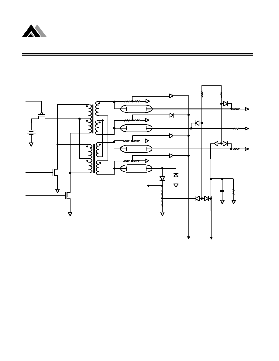
AME, Inc.
32
CCFL Backlight Controller
AME9002
Preliminary
Figure 21. Four Tube Power Section
D4
D5
Q3-2
Q3-1
Q2
To R7 and C8 integrator
T1
T2
V
Batt
R10
R9A
OUTA
OUTAPB
OUTC
To CSDET
R35
R36
R37
R38
R39
R50
R51
R52
To OVPL
OVPH
VDD
R9B
R9C
R9D
D20 D21
D23
D22
D24 D25
D26
R42
R43
C34
R40

AME, Inc.
33
AME9002
CCFL Backlight Controller
Preliminary
NODE A
NODE B
NODE C
1.25
Normal Operation
(Filtered Voltage > 1.25V
Ë
Ë
Ë
Ë
No Fault)
filtered
unfiltered
NODE A
NODE B
NODE C
No Current in TUBE B
1.25
unfiltered
filtered
One Tube Missing Operation
(Filtered Voltage < 1.25V
Ë
Ë
Ë
Ë
Fault)
Figure 22.

AME, Inc.
34
CCFL Backlight Controller
AME9002
Preliminary
n
Package Dimension
QSOP24
MIN
MAX
MIN
MAX
A
1.524
1.752
0.060
0.069
A1
0.101
0.228
0.004
0.009
A2
b
0.203
0.304
0.008
0.012
b1
0.203
0.279
0.008
0.011
c
0.177
0.254
0.007
0.010
c1
0.177
0.228
0.007
0.009
D
8.559
8.737
0.337
0.344
ZD
E
5.791
6.197
0.228
0.244
E1
3.810
3.987
0.150
0.157
L
0.406
1.270
0.016
0.050
L1
e
J
K
Ë
0
o
8
o
0
o
8
o
Ë1
5
o
15
o
5
o
15
o
Ë2
0
o
-
0
o
-
R
1.27REF
0.050REF
SYMBOLS
MILLIMETERS
INCHES
1.473REF
0.058REF
0.838REF
0.033REF
0.254BSC
0.010BSC
0.635BSC
0.025BSC
1.27REF
0.050REF
0.33 x 45
o
0.013 x 45
o
Top View
Bottom View
Side View
End View
Detail A
D
E1
E
K
J
See Detail A
b
e
ZD
A
A2
A1
c1
b1
(c)
(b)
c
L1
L
£
c
£ c
1
£ c
2
R

AME, Inc.
35
AME9002
CCFL Backlight Controller
Preliminary
n
Package Dimension
SOIC24
H
E
e
B
D
See Detail A
C
Pin No.1 Indentifier
A1
A2
A
Top View
Bottom View
Side View
End View
L
£
c
Detail A
MIN
MAX
MIN
MAX
A
2.35
2.65
0.092
0.104
A1
0.10
0.30
0.004
0.012
A2
2.25
2.31
0.089
0.091
B
0.33
0.51
0.013
0.020
C
0.23
0.32
0.009
0.013
D
15.20
15.60
0.598
0.614
E
7.40
7.60
0.291
0.299
e
H
10.00
10.65
0.394
0.419
L
0.40
1.27
0.016
0.050
0
o
8
o
0
o
8
o
1.27BSC
0.050BSC
SYMBOLS
MILLIMETERS
INCHES

AME, Inc.
36
CCFL Backlight Controller
AME9002
Preliminary
n
Package Dimension
PDIP24
MIN
MAX
MIN
MAX
A
-
6.35
-
0.250
A1
0.39
-
0.015
-
A2
3.18
4.95
0.125
0.195
b
0.35
0.56
0.014
0.022
b2
0.77
1.77
0.030
0.070
C
0.20
0.39
0.008
0.015
D
29.30
32.70
1.154
1.287
D1
0.13
-
0.005
-
E
15.24
15.87
0.600
0.625
E1
12.32
14.73
0.485
0.580
e
eB
15.24
17.78
0.600
0.700
L
2.93
5.08
0.115
0.200
1
1
1
1
2
2
2
2
SYMBOLS
MILLIMETERS
INCHES
2.54BSC
0.100BSC
7
o
7
o
7
o
7
o
E1
CL
R1.524 x 0.762 DP
(R0.060 x 0.030") DP
b
b2
e
D
D1
A2
A
L
£ c
1
A1
Base Plane
Seating Plane
Top View
Side View
End View
E
(Outer to Outer)
£ c
2
c
eB

Life Support Policy:
These products of AME, Inc. are not authorized for use as critical components in life-support devices or sys-
tems, without the express written approval of the president
of AME, Inc.
AME, Inc. reserves the right to make changes in the circuitry and specifications of its devices and
advises its customers to obtain the latest version of relevant information.
©
AME, Inc. , May 2004
Document: 2023-DS9002-B
Corporate Headquarter
U.S.A.(Subsidiary)
AME, Inc.
Analog Microelectronics, Inc.
2F, 302 Rui-Guang Road, Nei-Hu District 3100 De La Cruz Blvd., Suite 201
Taipei 114, Taiwan, R.O.C. Santa Clara, CA. 95054-2046
Tel: 886 2 2627-8687 Tel : (408) 988-2388
Fax: 886 2 2659-2989
Fax: (408) 988-2489
www.ame.com.tw
E-Mail: sales@ame.com.tw