 | –≠–ª–µ–∫—Ç—Ä–æ–Ω–Ω—ã–π –∫–æ–º–ø–æ–Ω–µ–Ω—Ç: MSA-1023 | –°–∫–∞—á–∞—Ç—å:  PDF PDF  ZIP ZIP |
Document Outline
- List of Figures
- 1. Typical Gain vs. Power Out
- 2. Device Current vs. Voltage
- 3. Output Power at 1 dB Gain Compression, Third Order Intercept Point vs. Current
- 4. Output Power at 1 dB Gain Compression vs. Temperature
- 5. Gain vs. Frequency
- 6. VSWR vs. Frequency
- Features
- Description
- Typical Push-Pull Biasing Configuration
- 230 mil BeO Flange Package
- MSA-1023 Absolute Maximum Ratings
- Electrical Specifications
- MSA-1023 Typical Scattering Parameters
- Typical Performance
- 230 mil BeO Flange Package

6-446
Cascadable Silicon Bipolar
MMIC Amplifier
Technical Data
Features
∑ High Output Power:
+27 dBm Typical P
1dB
at 1.0 GHz
∑ Low Distortion:
37 dBm Typical IP
3
at 1.0 GHz
∑ 8.5 dB Typical Gain at
1.0 GHz
∑ Hermetic, Metal/Beryllia
Stripline Package
∑ Impedance Matched to 25
for Push-Pull Configurations
MSA-1023
230 mil BeO Flange
Package
Description
The MSA-1023 is a high perfor-
mance, medium power silicon
bipolar Monolithic Microwave
Integrated Circuit (MMIC) housed
in a hermetic, BeO flange package
for good thermal characteristics.
Typical Push-Pull Biasing Configuration
C
block
C
block
C
block
C
block
R
bias
R
bias
V
CC
>
20
V
V
d
= 15 V
RFC
50
RFC
IN
OUT
V
CC
>
20
V
MSA
MSA
4
1
1
2
4
3
3
2
50
This MMIC is designed for use in a
push-pull configuration in a 25
system. The MSA-1023 can also be
used as a single-ended amplifier in
a 50
system with slightly
reduced performance. Typical
applications include narrow and
broadband RF amplifiers in
industrial and military systems.
The MSA-series is fabricated using
HP's 10 GHz f
T
, 25 GHz f
MAX
,
silicon bipolar MMIC process
which uses nitride self-alignment,
ion implantation, and gold metalli-
zation to achieve excellent
performance, uniformity and
reliability. The use of an external
bias resistor for temperature and
current stability also allows bias
flexibility.
5965-9554E
6-447
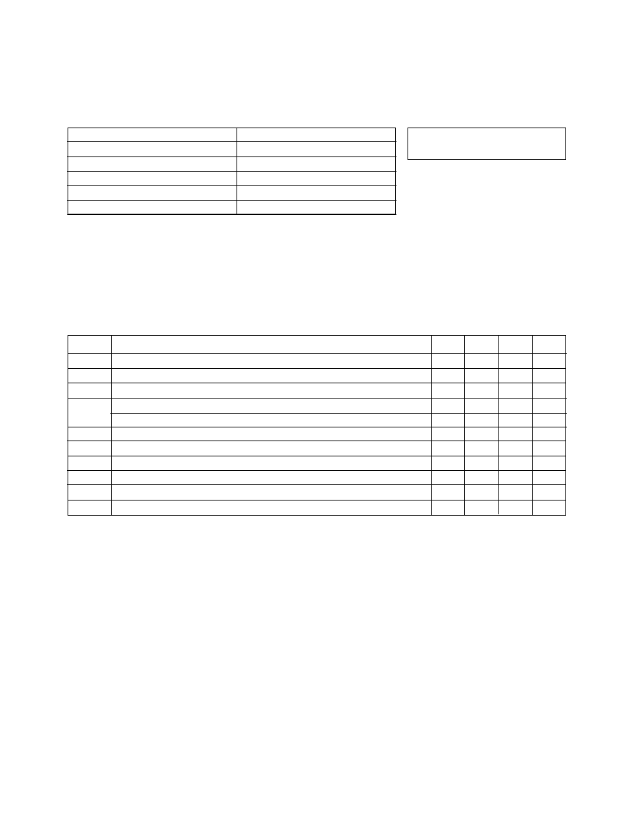
MSA-1023 Absolute Maximum Ratings
Parameter
Absolute Maximum
[1]
Device Current
425 mA
Power Dissipation
[2,3]
7.0 W
RF Input Power
+25 dBm
Junction Temperature
200
∞
C
Storage Temperature
≠65 to 200
∞
C
Thermal Resistance
[2,4]
:
jc
= 15
∞
C/W
G
P
Power Gain (|S
21
|
2
)
f = 1.0 GHz
dB
7.5
8.5
9.5
G
P
Gain Flatness
f = 0.1 to 2.0 GHz
dB
±
0.6
f
3 dB
3 dB Bandwidth
[2]
GHz
2.5
Input VSWR
f = 0.1 to 2.0 GHz
2.0:1
Output VSWR
f = 0.1 to 2.0 GHz
2.8:1
NF
25
Noise Figure
f = 1.0 GHz
dB
7.0
P
1 dB
Output Power at 1 dB Gain Compression
f = 1.0 GHz
dBm
25.0
27.0
IP
3
Third Order Intercept Point
f = 1.0 GHz
dBm
37.0
t
D
Group Delay
f = 1.0 GHz
psec
250
V
d
Device Voltage
V
13.5
15.0
16.5
dV/dT
Device Voltage Temperature Coefficient
mV/
∞
C
≠18.0
Notes:
1. The recommended operating current range for this device is 150 to 400 mA. Typical performance as a function of
current is on the following page.
2. Referenced from 10 MHz gain (G
P
).
Electrical Specifications
[1]
, T
A
= 25
∞
C
Symbol
Parameters and Test Conditions: I
d
= 325 mA, Z
O
= 25
Units
Min.
Typ.
Max.
VSWR
Notes:
1. Permanent damage may occur if any of these limits are exceeded.
2. T
CASE
= 25
∞
C.
3. Derate at 66.7 mW/
∞
C for T
C
> 95
∞
C.
4. The small spot size of this technique results in a higher, though more
accurate determination of
jc
than do alternate methods. See MEASURE-
MENTS section "Thermal Resistance" for more information.
6-448
MSA-1023 Typical Scattering Parameters (Z
O
= 50
, T
A
= 25
∞
C, I
d
= 325 mA)
Freq.
GHz
Mag
Ang
dB
Mag
Ang
dB
Mag
Ang
Mag
Ang
k
0.001
.40
≠121
15.3
5.85
149
≠17.9
.128
22
.42
≠99
0.69
0.005
.51
≠167
8.5
2.67
156
≠15.9
.160
6
.45
≠161
1.05
0.010
.52
≠174
7.5
2.36
166
≠15.8
.162
3
.45
≠171
1.16
0.025
.52
≠178
7.2
2.28
172
≠15.8
.162
1
.45
≠177
1.20
0.050
.52
179
7.1
2.26
173
≠15.8
.161
≠1
.45
≠179
1.21
0.100
.53
176
7.0
2.25
170
≠15.8
.161
≠3
.45
179
1.21
0.200
.53
172
7.0
2.25
163
≠15.8
.161
≠5
.46
174
1.21
0.400
.51
164
7.0
2.24
146
≠15.8
.161
≠11
.46
170
1.22
0.600
.48
157
7.0
2.24
130
≠16.0
.159
≠16
.45
165
1.23
0.800
.45
151
7.0
2.23
113
≠16.1
.157
≠21
.44
161
1.24
1.000
.42
146
7.0
2.23
95
≠16.2
.155
≠26
.44
157
1.24
1.200
.38
144
6.9
2.22
78
≠16.4
.151
≠31
.44
155
1.24
1.400
.35
145
6.8
2.20
61
≠16.7
.146
≠36
.45
154
1.24
1.600
.34
149
6.6
2.15
44
≠17.0
.141
≠41
.46
153
1.22
1.800
.36
152
6.3
2.07
19
≠17.3
.136
≠45
.49
150
1.18
2.000
.39
153
5.9
1.97
11
≠17.7
.130
≠49
.62
148
1.13
2.500
.51
148
4.6
1.69
≠24
≠18.3
.121
≠52
.52
140
.91
3.000
.60
133
3.0
1.41
≠57
≠17.9
.127
≠57
.70
128
.59
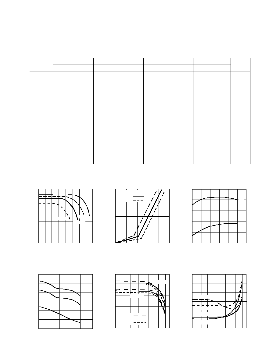
A model for this device is available in the DEVICE MODELS section.
S
11
S
21
S
12
S
22
Typical Performance, T
A
= 25
∞
C
(unless otherwise noted)
GAIN (dB)
18
16
20
22
26
28
24
30
32
POWER OUT (dBm)
Figure 1. Typical Gain vs. Power Out,
Z
O
= 25
∞
, I
d
= 325 mA.
200
150
250
300
350
400
I
d
(mA)
Figure 3. Output Power at 1 dB
Gain Compression, Third Order
Intercept Point vs. Current,
Z
O
=25
, f = 1.0 GHz.
0
2
4
6
8
10
20
24
28
36
32
40
0.5 GHz
0.5 GHz
Figure 4. Output Power at 1 dB Gain
Compression vs. Temperature,
Z
O
= 25
, I
d
= 325 mA.
FREQUENCY (GHz)
Figure 5. Gain vs. Frequency,
I
d
= 325 mA.
0.1
0.2 0.3
0.5
2.0
1.0
4.0
0
8
10
6
4
2
GAIN
(dB)
I
d
= 325 mA
I
d
= 150 mA
20
22
24
26
28
30
32
+25
≠50
+100
P
1 dB
(dBm)
TEMPERATURE (
∞
C)
2.0 GHz
1.0 GHz,
4.0 GHz
1.0 GHz
P
1 dB
I
d
= 400 mA
1.0 GHz
1.5 GHz
2.0 GHz
P
1 dB
(dBm)
IP
3
(dBm)
IP
3
FREQUENCY (GHz)
Figure 6. VSWR vs. Frequency,
I
d
= 325 mA.
0.1
0.2 0.3
0.5
2.0
1.0
3.0
0
5
6
4
3
2
1
VSWR
Input Z
O
= 50
Output Z
O
= 25
2
0
4
6
8
10
V
d
(V)
Figure 2. Device Current vs. Voltage.
0
100
200
300
400
I
d
(mA)
T
C
= +100
∞
C
T
C
= +25
∞
C
T
C
= ≠50
∞
C
Input Z
O
= 25
Output Z
O
= 50
Z
O
= 25
Z
O
= 50
6-449
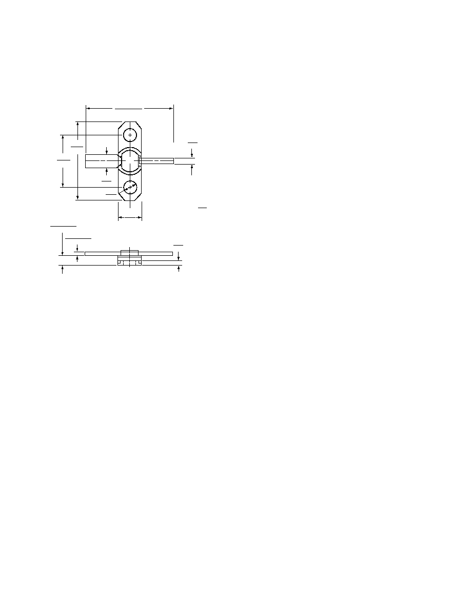
230 mil BeO Flange Package
1
3
4
2
GROUND
RF OUTPUT
AND BIAS
RF
INPUT
.230
5.84
.120
3.05
Notes:
(unless otherwise specified)
1. Dimensions are in
2. Tolerances
in .xxx =
±
0.005
mm .xx =
±
0.13
mm
.060
1.52
.004
±
.002
.10
±
.05
.130
±
.010
3.30
±
.25
.800
20.32
.562
14.27
.050
1.27
GROUND
.130
3.30
.725
±
.030
18.42
±
.76