 | –≠–ª–µ–∫—Ç—Ä–æ–Ω–Ω—ã–π –∫–æ–º–ø–æ–Ω–µ–Ω—Ç: MSA-0404 | –°–∫–∞—á–∞—Ç—å:  PDF PDF  ZIP ZIP |
Document Outline
- List of Figures
- 1. Typical Power Gain vs. Frequency
- 2. Device Current vs. Voltage
- 3. Power Gain vs. Current
- 4. Output Power at 1 dB Gain Compression, NF and Power Gain vs. Case Temperature
- 5. Output Power at 1 dB Gain Compression vs. Frequency
- 6. Noise Figure vs. Frequency
- Features
- Description
- Typical Biasing Configuration
- 04A Plastic Package
- MSA-0404 Absolute Maximum Ratings
- Electrical Specifications
- MSA-0404 Typical Scattering Parameters
- Typical Performance
- 04A Plastic Package Dimensions

6-322
Cascadable Silicon Bipolar
MMIC Amplifier
Technical Data
Features
∑ Cascadable 50
Gain Block
∑ 3 dB Bandwidth:
DC to 2.5 GHz
∑ 7.5 dB Typical Gain at
1.0 GHz
∑ 11.5 dBm Typical P
1 dB
at
1.0 GHz
∑ Unconditionally Stable
(k>1)
∑ Low Cost Plastic Package
MSA-0404
04A Plastic Package
Description
The MSA-0404 is a high perfor-
mance silicon bipolar Monolithic
Microwave Integrated Circuit
(MMIC) housed in a low cost
Typical Biasing Configuration
C
block
C
block
R
bias
V
CC
>
7 V
V
d
= 5.25 V
RFC (Optional)
IN
OUT
MSA
4
1
2
3
plastic package. This MMIC is
designed for use as a general
purpose 50
gain block. Typical
applications include narrow and
broad band IF and RF amplifiers
in commercial and industrial
applications.
The MSA-series is fabricated using
HP's 10 GHz f
T
, 25 GHz f
MAX
,
silicon bipolar MMIC process
which uses nitride self-alignment,
ion implantation, and gold metalli-
zation to achieve excellent
performance, uniformity and
reliability. The use of an external
bias resistor for temperature and
current stability also allows bias
flexibility.
5965-9573E
6-323
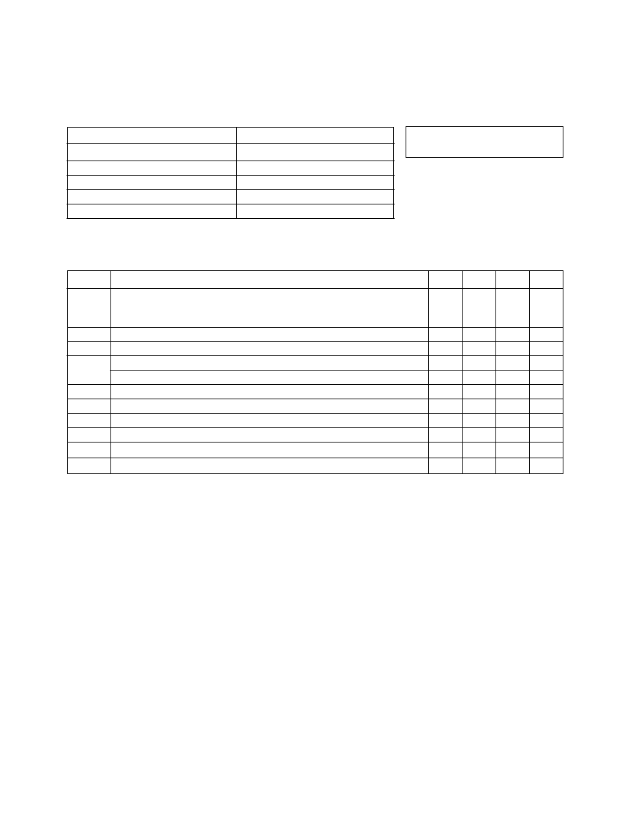
MSA-0404 Absolute Maximum Ratings
Parameter
Absolute Maximum
[1]
Device Current
85 mA
Power Dissipation
[2,3]
500 mW
RF Input Power
+13 dBm
Junction Temperature
150
∞
C
Storage Temperature
≠65 to 150
∞
C
Thermal Resistance
[2,4]
:
jc
= 85
∞
C/W
Notes:
1. Permanent damage may occur if
any of these limits are exceeded.
2. T
CASE
= 25
∞
C.
3. Derate at 10 mW/
∞
C for T
C
> 108
∞
C.
4. See MEASUREMENTS section
"Thermal Resistance" for more
information.
G
P
Power Gain (|S
21
|
2
)
f = 0.1 GHz
dB
8.3
f = 0.5 GHz
7.0
8.0
f = 1.0 GHz
7.5
G
P
Gain Flatness
f = 0.1 to 2.0 GHz
dB
±
1.0
f
3 dB
3 dB Bandwidth
GHz
2.5
Input VSWR
f = 0.1 to 2.5 GHz
1.4:1
Output VSWR
f = 0.1 to 2.5 GHz
1.8:1
NF
50
Noise Figure
f = 1.0 GHz
dB
7.0
P
1 dB
Output Power at 1 dB Gain Compression
f = 1.0 GHz
dBm
11.5
IP
3
Third Order Intercept Point
f = 1.0 GHz
dBm
24.5
t
D
Group Delay
f = 1.0 GHz
psec
150
V
d
Device Voltage
V
4.75
5.25
5.75
dV/dT
Device Voltage Temperature Coefficient
mV/
∞
C
≠8.0
Note:
1. The recommended operating current range for this device is 30 to 70 mA. Typical performance as a function of current
is on the following page.
Electrical Specifications
[1]
, T
A
= 25
∞
C
Symbol
Parameters and Test Conditions: I
d
= 50 mA, Z
O
= 50
Units
Min.
Typ.
Max.
VSWR
6-324
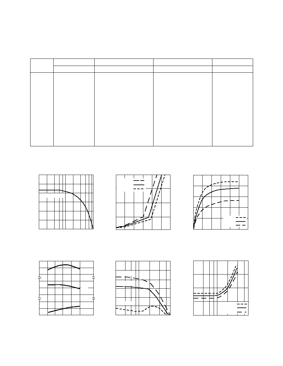
Typical Performance, T
A
= 25
∞
C
(unless otherwise noted)
0.1
0.3 0.5
1.0
3.0
6.0
0
2
4
6
8
10
12
G
p
(dB)
Figure 1. Typical Power Gain vs.
Frequency, T
A
= 25
∞
C, I
d
= 50 mA.
Gain Flat to DC
V
d
(V)
Figure 2. Device Current vs. Voltage.
0
20
40
60
80
I
d
(mA)
2
3
4
5
6
7
1
T
C
= +85
∞
C
T
C
= +25
∞
C
T
C
= ≠25
∞
C
I
d
(mA)
Figure 3. Power Gain vs. Current.
4
5
6
7
8
9
G
p
(dB)
20
40
50
60
70
30
6
7
8
10
11
12
≠25
0
+25
+55
+85
6
7
8
P
1 dB
(dBm)
NF (dB)
NF
G
p
(dB)
TEMPERATURE (
∞
C)
Figure 4. Output Power at 1 dB Gain
Compression, NF and Power Gain vs.
Case Temperature, f = 1.0 GHz,
I
d
=50mA.
P
1 dB
G
P
0.1
0.2 0.3
0.5
2.0
1.0
4.0
FREQUENCY (GHz)
FREQUENCY (GHz)
Figure 5. Output Power at 1 dB Gain
Compression vs. Frequency.
3
6
9
12
15
18
21
P
1 dB
(dBm)
I
d
= 70 mA
I
d
= 30 mA
I
d
= 50 mA
6.5
6.0
7.0
7.5
8.0
NF (dB)
FREQUENCY (GHz)
Figure 6. Noise Figure vs. Frequency.
0.1
0.2 0.3
0.5
2.0
1.0
4.0
I
d
= 30 mA
I
d
= 50 mA
I
d
= 70 mA
0.1 GHz
1.0 GHz
2.0 GHz
MSA-0404 Typical Scattering Parameters (Z
O
= 50
, T
A
= 25
∞
C, I
d
= 50 mA)
Freq.
GHz
Mag
Ang
dB
Mag
Ang
dB
Mag
Ang
Mag
Ang
0.1
.16
175
8.3
2.59
174
≠16.2
.156
0
.13
≠13
0.2
.16
170
8.2
2.58
168
≠16.2
.155
2
.13
≠25
0.4
.15
161
8.1
2.54
156
≠16.0
.158
4
.14
≠47
0.6
.14
152
8.0
2.51
145
≠16.0
.158
6
.16
≠64
0.8
.12
145
7.8
2.46
133
≠15.8
.163
8
.19
≠79
1.0
.11
141
7.7
2.41
122
≠15.4
.169
9
.21
≠91
1.5
.07
141
7.2
2.29
96
≠14.6
.186
13
.24
≠118
2.0
.09
161
6.6
2.14
71
≠13.3
.215
12
.26
≠140
2.5
.14
159
5.9
1.98
53
≠12.4
.240
13
.28
≠157
3.0
.22
148
5.1
1.80
33
≠11.7
.260
7
.29
≠176
3.5
.30
128
4.3
1.64
13
≠10.9
.286
0
.32
167
4.0
.38
109
3.2
1.45
≠6
≠10.4
.301
≠7
.33
153
5.0
.47
91
2.1
1.27
≠23
≠10.2
.310
≠15
.35
137
6.0
.55
75
1.0
1.09
≠39
≠10.1
.312
≠24
.37
120
A model for this device is available in the DEVICE MODELS section.
S
11
S
21
S
12
S
22
6-325
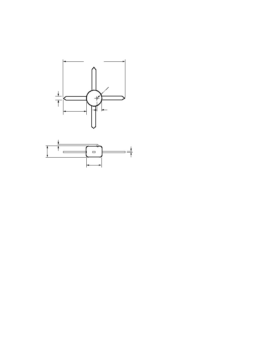
04A Plastic Package Dimensions
1
4
3
0.76 (0.030)
0.20
±
0.050
(0.008
±
0.002)
3.68
(0.145)
2.54
±
0.25
(0.100
±
0.010)
12.39
±
0.76
(0.488
±
0.030)
1
2
0.51
(0.020)
0.96 (0.038)
4.29
(0.169)
0.76 (0.030)
DIA.
DIMENSIONS ARE IN MILLIMETERS (INCHES).
RF INPUT
RF OUTPUT
& BIAS
GROUND
GROUND
NOTES:
(UNLESS OTHERWISE SPECIFIED)
1. DIMENSIONS ARE IN
MILLIMETERS (INCHES)
2. TOLERANCES
mm .XX =
±
0.13
in .XXX =
±
0.005
4