 | –≠–ª–µ–∫—Ç—Ä–æ–Ω–Ω—ã–π –∫–æ–º–ø–æ–Ω–µ–Ω—Ç: IFD-53110 | –°–∫–∞—á–∞—Ç—å:  PDF PDF  ZIP ZIP |
Document Outline
- List of Figures
- 1. Input Sensitivity vs. Input Frequency and Recommended Operating Ranges for Nominal Operating Ranges. . .
- 2. Input Sensitivity vs. Input Frequency and Recommended Operating Ranges. . .
- 3. Input Sensitivity vs. Input Frequency and Temperature
- 4. Device Current vs. Voltage and Temperature
- 5. Input and Output VSWR vs. Frequency
- 6. Output Power Level vs. Input Frequency. . .
- 7. SSB Phase Noise vs. Offset Frequency, and Input Frequency.
- 8. IFD-53010 Typical Output Response with 5 GHz Input.
- 9. Typical ECL Biasing Configuration, IFD-53010 and IFD-53110.
- 10. Typical RF Biasing Configuration, IFD-53010 and IFD-53110.
- 11. Typical Stabilized LO Configuration, IFD-53010 and IFD-53110.
- 12. Sensitivity Test Configuration, IFD-53010 and IFD-53110.
- Features
- Functional Block Diagram
- 100 mil Stripline Package
- Pin Configuration
- Description
- Absolute Maximum Ratings
- Guaranteed Electrical Specifications
- Typical Design Information
- Typical Performance
- Package Dimensions

7-151
Silicon Bipolar MMIC
3.5 and 5.5 GHz Divide-by-4
Static Prescalers
Technical Data
IFD-53010
IFD-53110
Features
∑ Wide Operating Frequency
Range:
IFD-53010: 0.15 to 5.5 GHz
IFD-53110: 0.15 to 3.5 GHz
∑ Low Phase Noise:
-143 dBc/Hz @ 1 kHz Offset
∑ Output Power: -5 dBm Typ.
∑ Single Supply Voltage
V
cc
= 5 V or V
ee
= -5 V
∑ On-Chip Terminations
Provide Good Input and
Output VSWRs
∑ Hermetic Gold-Ceramic
Surface Mount Package
100 mil Stripline Package
Description
Hewlett-Packard's IFD-53010 and
IFD-53110 are low phase noise
silicon bipolar static digital
frequency dividers using two
scaled Emitter-Coupled-Logic
(ECL) master-slave D flip-flops
and buffer amplifiers. They are
housed in hermetic high reliability
surface mount packages suitable
for commercial, industrial, and
military applications. Typical
applications include stabilized or
digitally controlled local oscil-
lators for GPS, SATCOM or
military receivers, and frequency
synthesizers and counters in
instrumentation systems. The
IFD-53110 is a lower cost selected
version of the IFD-53010, and is
distinguished by a reduced
operating frequency range.
The IFD series of frequency
dividers is fabricated using
Hewlett-Packard's 18 GHz, f
t
,
ISOSATTM-2 silicon bipolar
process which uses nitride self-
alignment, submicrometer
lithography, trench isolation, ion-
implantation, gold metallization
and polyimide intermetal
dielectric and scratch protection
to achieve excellent device
uniformity, performance, and
reliability.
Functional Block Diagram
Pin Configuration
V
EE
RF INPUT
RF OUTPUT
1
2
3
4
V
CC
C
Q
C
Q
C
Q
C
Q
4
1
2
3
V
CC
V
EE
RF INPUT
RF OUTPUT
5965-9115E

7-152
Absolute Maximum Ratings
Symbol
Parameter
Units
Absolute Maximum
[1]
V
cc
- V
ee
Device Voltage
V
8
P
diss
Power Dissipation
[2,3]
mW
650
P
in
RF Input Power
dBm
+15
T
j
Junction Temperature
∞
C
200
T
STG
Storage Temperature
∞
C
-65 to +200
Thermal Resistance
[2]
:
jc
= 107
∞
C/W
Notes:
1, Operation of this device above any one of these parameters may cause permanent damage.
2. T
case
= 25
∞
C.
3. Derate at 9.3 mW/
∞
C for T
C
130
∞
C.
Typical Design Information
, T
A
= 25
∞
C, Z
0
= 50
, V
cc
- V
ee
= 5.0 V, P
in
= -10 dBm.
All values apply to both IFD-53010 and IFD-53110. f
test
is 5 GHz for IFD-53010 and 3 GHz for IFD-53110 (unless
otherwise noted).
Symbol
Parameters and Test Conditions
Units
Value
F
MIN
Minimum Clock Frequency
[1]
MHz
150
P
in
Input Sensitivity
f = f
test
dBm
-22
mVpp
50
P
out
Output Power
f = 0.15 to f
test
dBm
-5
mVpp
355
VSWR
Input VSWR
f = 0.15 to f
test
2.0:1
Output VSWR
f = 0.15 to f
test
2.5:1
PN
SSB Phase Noise
f = 3 GHz, 1 kHz offset
dBc/Hz
-143
f = 5 GHz, 1 kHz offset (IFD-53010 only)
-138
T
r
Output Rise Time, 20% - 80%
f = f
test
psec
145
T
f
Output Fall Time, 20% - 80%
f = f
test
psec
85
Note:
1. Minimum clock frequency when driven from a sinusoidal input. Operation to lower frequencies is possible when using input signals
with faster rise times, such as occurs in the case of a cascade of two or more IFDs.
Guaranteed Electrical Specifications,
IFD-53010 and IFD-53110
T
A
= 25
∞
C, Z
O
= 50
, V
cc
- V
ee
= 5.0 V
Symbol
Parameters and Test Conditions
Units
Min.
Typ.
Max.
IFD-53010:
F
MAX
Maximum Clock Frequency
P
in
= -10 dBm (200 mVpp)
GHz
5.5
6.0
IFD-53110:
F
MAX
Maximum Clock Frequency
P
in
= -10 dBm (200 mVpp)
GHz
3.5
5.0
I
CC
IFD-53010 and IFD-53110: Supply Current
mA
35
43
50
7-153
Typical Performance,
T
A
= 25
∞
C, Z
O
= 50
, V
cc
- V
ee
= 5.0 V
Graphs apply to both IFD-53010 and IFD-53110 (unless otherwise noted).
Figure 8. IFD-53010 Typical Output Response with 5 GHz Input.
Figure 7. SSB Phase Noise vs. Offset
Frequency, and Input Frequency.
Figure 4. Device Current vs. Voltage
and Temperature.
Figure 6. Output Power Level vs. Input
Frequency and V
cc
- V
ee
.
Figure 5. Input and Output VSWR vs.
Frequency.
Figure 1. Input Sensitivity vs. Input
Frequency and Recommended
Operating Ranges for Nominal
Operating Conditions (T = 25
∞
C , V
cc
-
V
ee
= 5 V).
Figure 3. Input Sensitivity vs. Input
Frequency and Temperature
(V
cc
- V
ee
= 5 V).
Figure 2. Input Sensitivity vs. Input
Frequency and Recommended
Operating Ranges for Worst Case
Operating Conditions (-55
∞
C < T <
125
∞
C and 4.5 V < V
cc
- V
ee
< 5.5 V.
0
-10
-20
-30
-40
-50
0
1
2
3
4
5
6
7
FREQUENCY (GHz)
INPUT SENSITIVITY (dBm)
IFD-53010 &
IFD-53110
IFD-53010
0
-10
-20
-30
-40
-50
0
1
2
3
4
5
6
7
FREQUENCY (GHz)
INPUT SENSITIVITY (dBm)
IFD-53010 &
IFD-53110
IFD-53010
0
-10
-20
-30
-40
-50
0
1
2
3
4
5
6
7
FREQUENCY (GHz)
INPUT SENSITIVITY (dBm)
-55∞C
25∞C
125∞C
70
60
50
40
30
20
10
0
1
2
3
4
5
6
0
CC
V
-V
EE
(V)
CC
I (mA)
+ 125∞C
- 55∞C
+ 25∞C
3:1
2:1
1:1
10
100
1000
10000
OUTPUT
INPUT
FREQUENCY (MHz)
VSWR
0
-4
-8
10
100
1000
10000
5.0 V
4.5 V
FREQUENCY (MHz)
5.5 V
2
-2
-6
OUTPUT LEVEL (dBm)
60
80
-100
-120
-140
-160
1
1kHz
1MHz
OFFSET FREQUENCY
SSB PHASE NOISE (dBc/Hz)
5 GHz (IFD-53010)
-
-
2 TO 4 GHz
(IFD-53010 & IFD-53110)
+100
0
-100
TIME (psec)
+200
0
-200
200
V in
V (mV)
in
V (mV)
out
out
V
7-154
Figure 9. Typical ECL Biasing Configuration, IFD-53010 and IFD-53110.
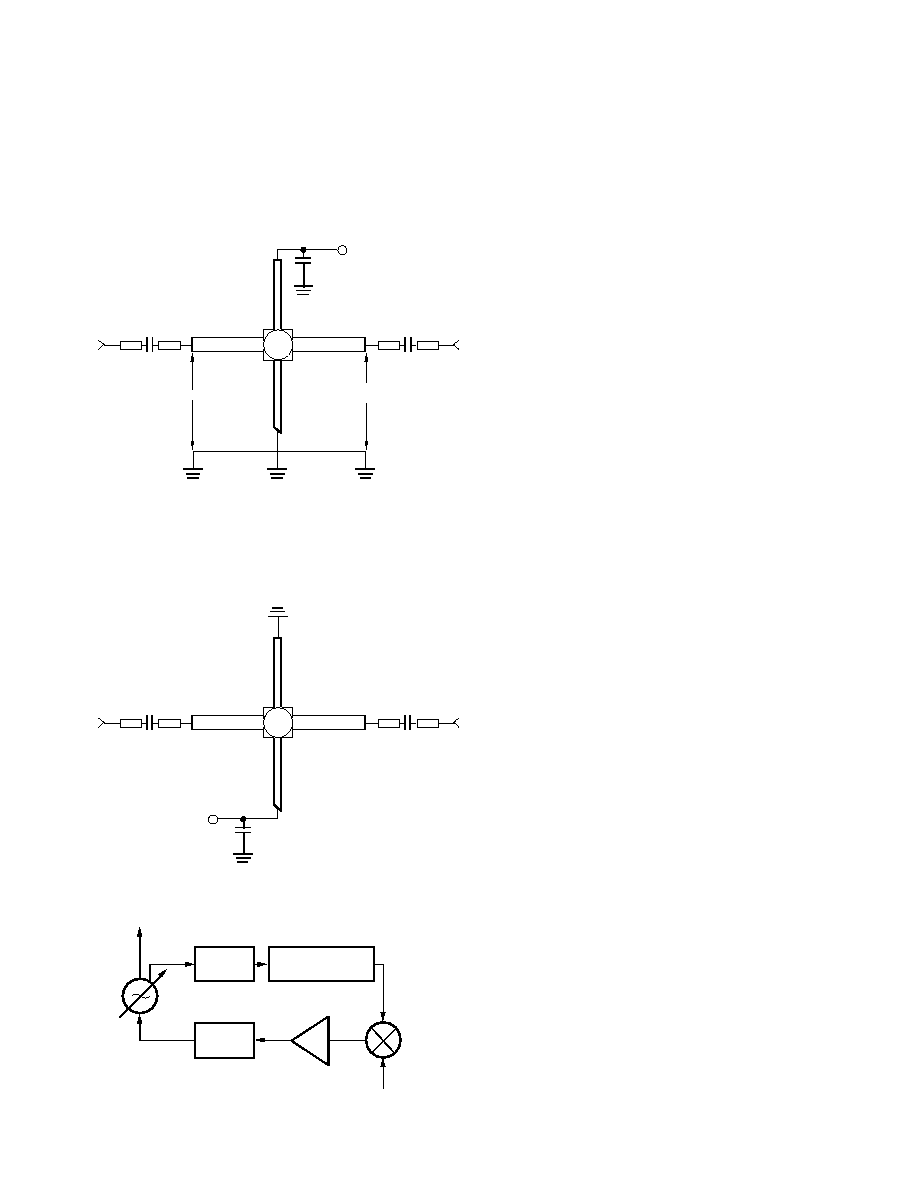
Figure 11. Typical Stabilized LO Configuration, IFD-53010 and IFD-53110.
Figure 10. Typical RF Biasing Configuration, IFD-53010 and IFD-53110.
4
1
3
2
V = -5.0 V
EE
C
BL
C
BY
(47 nF min.)
V = 0 V
CC
PIN:
CC
V
F
RF INPUT
(50 )
C
BL
F/4
RF OUTPUT
(50 )
SWINGS BETWEEN V
AND V -360 mV
CC
CC
BLOCKING CAPACITORS ARE 1000 pF TYP.
BYPASS CAPACITORS ARE 47 nF min.
BLOCKING CAPACITORS MAY BE OMITTED
IF GENERATOR AND LOAD ARE AT V LEVEL.
TRANSMISSION LINES ARE 50 .
CC
4
1
3
2
V = 5.0 V
CC
C
BL
C
BY
(47 nF min.)
PIN:
F
RF INPUT
(50 )
C
BL
F/4
RF OUTPUT
(50 )
BLOCKING CAPACITORS ARE 1000 pF TYP.
BYPASS CAPACITOR SHOULD BE 47 nF min.
TO ENSURE GOOD SENSITIVITY PERFORMANCE.
TRANSMISSION LINES ARE 50 .
V = 0 V
EE
LO OUTPUT
DIV. BY 4
PROGRAMMABLE
DIVIDER
LPF
VCO
PHASE DETECTOR
STABLE REFERENCE
AFC

7-155
Figure 12. Sensitivity Test Configuration, IFD-53010 and IFD-53110.
Package Dimensions
100 mil Stripline Package
O
5
4
1
2
V = -5.0 V
EE
V = 0 V
CC
PIN: 3
OUT
P
GENERATOR OUTPUT:
FREQUENCY = f
LEVEL = P + 10 dB (INTO 50 LOAD)
in
in
Z = 50
O
TEST SYSTEM
Z = 50
10 dB
SPECTRUM
ANALYZER
10 dB
f/4
1.02
(0.040)
0.51
(0.20)
0.76
(0.030)
0.10 ± 0.05
(0.004 ± 0.002)
12.57 ± 0.76
(0.495 ± 0.030)
2.54
(0.100)
NOTES: (unless otherwise specified)
1. DIMENSIONS ARE IN mm (INCHES)
2. TOLERANCES: in .xxx = ± .005
mm .xx = ± .13
4
1
3
2