 | –≠–ª–µ–∫—Ç—Ä–æ–Ω–Ω—ã–π –∫–æ–º–ø–æ–Ω–µ–Ω—Ç: HMMC-3104 | –°–∫–∞—á–∞—Ç—å:  PDF PDF  ZIP ZIP |

6-67
Absolute Maximum Ratings
[1]
(@ T
A
=25
∞
C, unless otherwise indicated)
[1]
Operation in excess of any parameter limit (except T
BS
) may cause permanent damage
to the device.
Symbol
Parameters/Conditions
Min.
Max.
Units
V
CC
Bias Supply Voltage
+7
volts
V
EE
Bias Supply Voltage
-7
volts
|V
CC
-
V
EE
|
Bias Supply Delta
+7
volts
V
Logic
Logic Threshold Voltage
V
CC
-1.5
V
CC
-1.2
volts
P
in(CW)
CW RF Input Power
+10
dBm
V
RFin
DC Input Voltage
(@ RF
in
or RF
in
Ports)
V
CC
±
0.5
volts
T
BS
[2]
[2]
MTTF >5
◊
10
5
hours @ T
BS
<85
∞
C. Operation in excess of maximum operating temper-
ature (T
BS
) will degrade MTTF.
Backside Operating Temp.
-40
+85
∞
C
T
st
Storage Temperature
-65
+165
∞
C
T
max
Maximum Assembly Temp.
(60 seconds max.)
310
∞
C
Description
The HMMC-3104 is a packaged
GaAs HBT MMIC prescaler
which offers DC to 16 GHz fre-
quency translation for use in
communications and EW sys-
tems incorporating high-frequen-
cy PLL oscillator circuits and
signal-path down conversion ap-
plications. The prescaler pro-
vides a large input power
sensitivity window and low
phase noise.
Package Type:
8-lead SSOP Plastic
Package Dimensions: 4.9
◊
3.9 mm Typ.
Package Thickness:
1.55 mm Typ.
Lead Pitch:
1.25 mm Nom.
Lead Width:
0.42 mm Nom.
Agilent HMMC-3104
DC - 16 GHz Packaged
Divide-by-4 Prescaler
HMMC-3104-TR1 - 7" diameter reel/500 each
HMMC-3104-BLK - Bubble strip/10 each
Data Sheet
Features
∑ Wide Frequency Range:
0.2≠16 GHz
∑ High Input Power
Sensitivity:
On-chip pre- and post-amps
-20 to +10 dBm (1≠10 GHz)
-15 to +10 dBm (10≠12 GHz)
-10 to +5 dBm (12≠15 GHz)
∑ P
out
: +6 dBm (0.99 V
p-p
) will
drive ECL
∑ Low Phase Noise:
-153 dBc/Hz @ 100 kHz Offset
∑ (+) or (-) Single Supply Bias
with wide range:
4.5 to 6.5 V
∑ Differential I/0 with on-chip
50
matching
Agi
lent
6-68
TCHMMC-3104/rev.3.4
RF Specifications
(T
A
= 25
∞
C, Z
0
= 50
, V
CC
- V
EE
= 5.0 volts)
Symbol
Parameters/Conditions
Min.
Typ.
Max.
Units
in(max)
Maximum input frequency of operation
16
18
GHz
in(min)
Minimum input frequency of operation
[1]
(P
in
= -10 dBm)
[1]
For sine-wave input signal. Prescaler will operate down to D.C. for square-wave input signal. Minimum divide frequency limited by input
slew-rate.
0.2
0.5
GHz
Self-Osc.
Output Self-Oscillation Frequency
[2]
[2]
Prescaler can exhibit this output signal under bias in the absence of an RF input signal. This condition can be eliminated by use of the
Input DC offset technique described on page 3.
3.4
GHz
P
in
@ DC, (Square-wave input)
-15
>-25
+10
dBm
@
in
= 500 MHz, (Sine-wave input)
-15
>-20
+10
dBm
in
= 1 to 10 GHz
-15
>-25
+10
dBm
in
= 10 to 12 GHz
-10
>-15
+10
dBm
in
= 12 to 15 GHz
-4
>-10
+4
dBm
RL
Small-Signal Input/Output Return Loss
(@
in
<
12
GHz)
15
dB
S
12
Small-Signal Reverse Isolation
(@
in
<
12
GHz)
30
dB
N
SSB Phase noise (@ P
in
= 0 dBm, 100kHz offset
from a
out
= 1.2 GHz Carrier)
-153
dBc/Hz
Jitter
Input signal time variation @ zero-crossing
(
in
= 10 GHz, P
in
= -10 dBm)
1
ps
r
or
f
Output transition time (10% to 90% rise/fall time)
70
ps
P
out
[3]
[3]
Fundamental of output square wave's Fourier Series.
@
out
<
1 GHz
4
6
dBm
@
out
= 2.5 GHz
3.5
5.5
dBm
@
out
= 3.5 GHz
0
2.0
dBm
|V
out(p-p)
|
[4]
[4]
Square wave amplitude calculated from P
out
.
@
out
<1 GHz
0.99
volts
@
out
= 2.5 GHz
0.94
volts
@
out
= 3.5 GHz
0.63
volts
P
Spitback
out
power level appearing at RF
in
or RF
in
(@
in
12 GHz, Unused RF
out
or RF
out
unterminated)
-40
dBm
out
power level appearing at RF
in
or RF
in
(@
in
= 12 GHz, Both RF
out
& RF
out
terminated)
-47
dBm
P
feedthru
Power
level of
in
appearing at RF
out
or RF
out
(@
in
= 12 GHz, P
in
= 0 dBm, Referred to
P
in
(
in
))
-23
dBc
H
2
Second harmonic distortion output level
(@
out
= 3.0 GHz, Referred to P
out
(
out
))
-25
dBc
DC Specifications/Physical Properties
(T
A
= 25
∞
C, V
CC
- V
EE
= 5.0 volts, unless otherwise listed)
Symbol
Parameters/Conditions
Min.
Typ.
Max.
Units
V
CC
- V
EE
Operating bias supply difference
[1]
4.5
5.0
6.5
volts
|I
CC
| or |I
EE
| Bias supply current
68
80
92
mA
V
RFin(q)
V
RFout(q)
Quiescent DC voltage appearing at all RF ports
V
CC
volts
V
Logic
Nominal ECL Logic Level
(V
Logic
contact self-bias voltage, generated on-chip)
V
CC
- 1.45
V
CC
-1.35
V
CC
-1.25
volts
[1]
Prescaler will operate over full specified supply voltage range. V
CC
or V
EE
not to exceed limits specified in Absolute Maximum Ratings
section.
HMMC-3104/rev.3.4
6-69
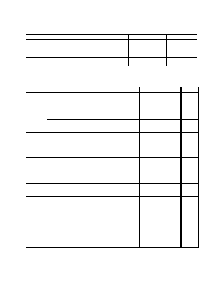
Figure 1.
Simplified Schematic
For positive supply operation,
V
CC
pins are nominally biased at
any voltage in the +4.5 to +6.5 volt
range with pin 8 (V
EE
)
grounded.
For negative bias operation V
CC
pins are typically grounded and a
negative voltage between -4.5 to -
6.5 volts is applied to pin 8 (V
EE
).
AC-Coupling and DC-
Blocking
All RF ports are DC connected
on-chip to the V
CC
contact
through on-chip 50
resistors.
Under any bias conditions where
VCC is not DC grounded the RF
ports should be AC coupled via
series capacitors mounted on the
PC-board at each RF port. Only
under bias conditions where V
CC
is DC grounded (as is typical for
negative bias supply operation)
may the RF ports be direct cou-
pled to adjacent circuitry or in
some cases, such as level shifting
to subsequent stages. In the latter
case the package heat sink may
be "floated" and bias applied as
the difference between V
CC
and
V
EE
.
Applications
The HMMC-3104 is designed for
use in high frequency communi-
cations, microwave instrumenta-
tion, and EW radar systems
where low phase-noise PLL con-
trol circuitry or broad-band fre-
quency translation is required.
Operation
The device is designed to operate
when driven with either a single-
ended or differential sinusoidal
input signal over a 200 MHz to 16
GHz bandwidth. Below 200 MHz
the prescaler input is "slew-rate"
limited, requiring fast rising and
falling edge speeds to properly di-
vide. The device will operate at
frequencies down to DC when
driven with a square-wave.
Due to the presence of an off-chip
RF-bypass capacitor inside the
package (connected to the V
CC
contact on the device), and the
unique design of the device itself,
the component may be biased
from either a single positive or
single negative supply bias. The
backside of the package is not DC
connected to any DC bias point
on the device.
Input DC Offset
If an RF signal with sufficient sig-
nal to noise ratio is present at the
RF input lead, the prescaler will
operate and provide a divided
output equal the input frequency
divided by the divide modulus.
Under certain "ideal" conditions
where the input is well matched
at the right input frequency, the
component may "self-oscillate",
especially under small signal in-
put powers or with only noise
present at the input This "self-os-
cillation" will produce a undes-
ired output signal also known as
a false trigger. To prevent false
triggers or self-oscillation condi-
tions, apply a 20 to 100 mV DC
offset voltage between the RF
in
and RF
in
ports. This prevents
noise or spurious low level sig-
nals from triggering the divider.
Adding a 10K
resistor between
the unused RF input to a contact
point at the V
EE
potential will re-
sult in an offset of
25mV be-
tween the RF inputs. Note
however, that the input sensitivi-
ty will be reduced slightly due to
the presence of this offset.
V
CC
V
CC
V
CC
V
EE
OUT
IN
IN
OUT
SOIC8 w/Backside GND
˜
6-70
TCHMMC-3104/rev.3.4
R
F
o
u
t
R
F
o
u
t
R
F
i
n
V
C
C
V
E
E
R
F
i
n
V
C
C
V
C
C
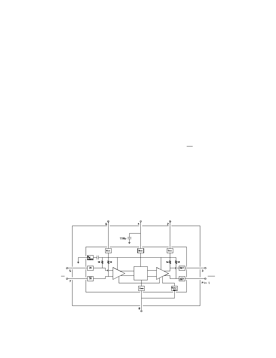
Figure 2.
Package & Dimensions
Notes:
∑ All dimensions in millimeters.
∑ Refer to JEDEC Outline MS-012 for
additional tolerances
∑ Exposed heat slug area on pkg bot-
tom = 2.67
◊
1.65.
∑ Exposed heat sink on package bot-
tom must be soldered to PCB rf
ground plane.
SYMBOL
MIN.
MAX.
A
1.35
1.75
A1
0.0
.25
B
0.33
0.51
C
0.19
.025
D
4.80
5.00
E
3.80
4.00
e
1.27 BSC
H
5.80
6.20
L
0.40
1.27
a
0
∞
8
∞
RFin
V
CC
(+4.5 to +6.5 volts)
~ 1
µ
f Monoblock
Capacitor
RFin
RFout
V
CC
V
CC
V
CC
RFout
V
EE
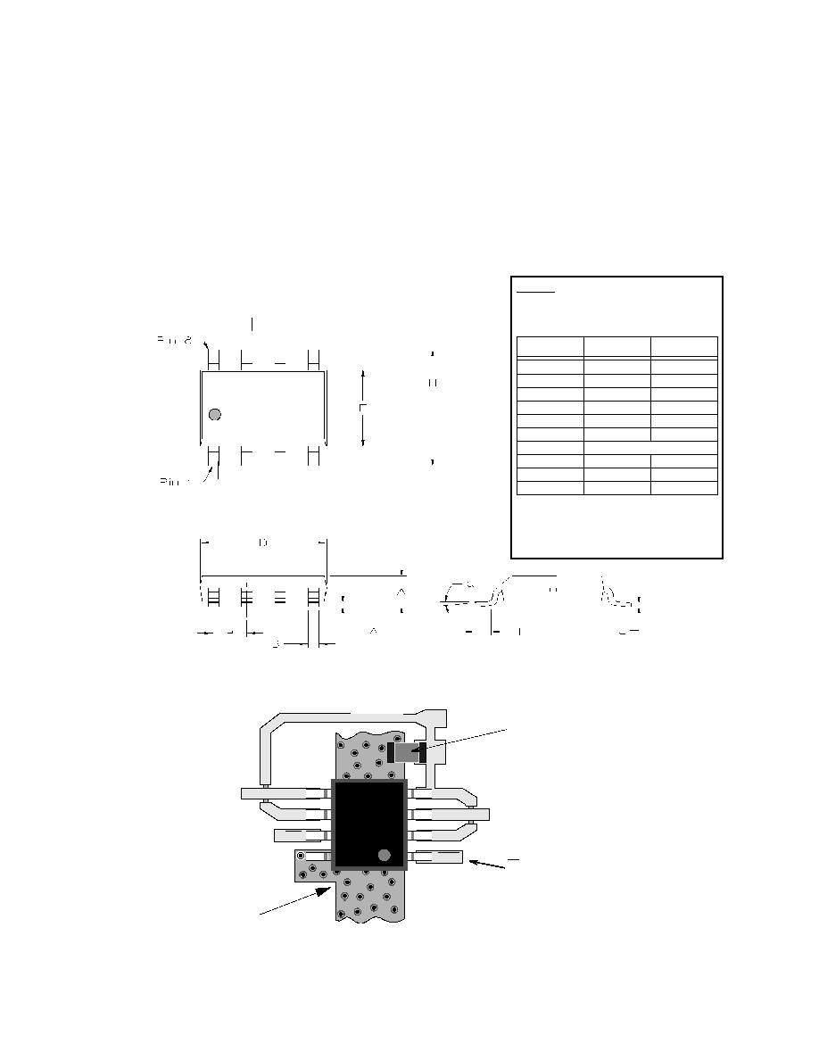
Figure 3.
Assembly Diagram
(Single-Supply, positive-bias configuration shown)
To operate component from a negative supply, ground
each V
CC
connection and supply V
EE
with a negative
voltage (-4.5 to -6.5v) bypassed to ground with ~ 1
µ
f capacitor.
RF
out
should be terminated in 50
to ground. (DC
blocking capacitor required for positive bias
configuration.)
9
6
1
8
H
M
M
C
-
3
1
0
4
Assembly Notes
Independent of the bias applied
to the package, the backside of
the package should always be
connected to both a good RF
ground plane and a good thermal
heat sinking region on the PC-
board to optimize performance.
For single-ended output opera-
tion the unused RF output lead
should be terminated into 50
to
a contact point at the V
CC
poten-
tial or to RF ground through a DC
blocking capacitor.
A minimum RF and thermal PC
board contact area equal to or
greater than 2.67 x 1.65 mm
(0.105" x 0.065") with eight 0.020"
diameter plated-wall thermal vias
is recommended.
MMIC ESD precautions, handling
considerations, die attach and
bonding methods are critical fac-
tors in successful GaAs MMIC
performance and reliability.
Agilent application note #54,
"GaAs MMIC ESD, Die Attach
and Bonding Guidelines" pro-
vides basic information on these
subjects.
Additional References:
PN #18, "HBT Prescaler Evalua-
tion Board."
A
g
i
l
e
n
t
Exposed heat sink on package bottom
must be soldered to PCB rf ground
plane.

HMMC-3104/rev.3.4
6-71
-8
-6
-4
-2
0
2
4
6
8
0
0.5
1
1.5
2
2.5
3
3.5
4
4.5
-100
-90
-80
-70
-60
-50
-40
-30
-20
-10
0
0
2
4
6
8
10
12
14
16
18
20
-40
-30
-20
-10
0
10
20
0
2
4
6
8
10
12
14
16
18
20
Period (200 pS / div.)
Figure 6.
Typical Output
Voltage Waveform
Figure 7.
HMMC-3104Output Power vs.
Output Frequency,
out
(GHz)
Figure 9.
Typical "Spitback" Power
P(
out
) appearing at RF input port
Supplemental Data:
V
CC
- V
EE
(volts)
I
S
u
p
p
l
y
(
m
A
)
V
L
o
g
i
c
-
V
C
C
(
v
o
l
t
s
)
Figure 5.
Typical Supply Current & V
Logic
vs. Supply Voltage
Figure 4.
Typical Input
Sensitivity Window
(V
CC
-V
EE
= +5 volts, T
A
=25
∞
C)
I
n
p
u
t
P
o
w
e
r
,
P
i
n
(
d
B
m
)
Input Frequency,
in
(GHz)
O
u
t
p
u
t
V
o
l
t
a
g
e
(
8
0
m
V
/
d
i
v
.
)
0
10
20
30
40
50
60
70
80
90
100
0
1
2
3
4
5
6
7
8
9
-2.0
-1.8
-1.6
-1.4
-1.2
-1.0
-0.8
-0.6
-0.4
-0.2
0.0
Output Frequency (GHz)
P
o
u
t
(
@
P
i
n
=
0
d
B
m
)
,
d
B
m
(V
CC
- V
EE
= +5 volts, T
A
=25
∞
C)
Input Frequency,
in
(GHz)
P
S
p
i
t
b
a
c
k
(
d
B
m
)
(V
CC
-V
EE
+5 volts, P
in
=0 dBm,T
A
=25
∞
C)
Both RFout Ports Terminated
Unterminated RFout Port
-10
-20
-30
-40
-50
-60
-70
-80
-90
-100
0
2
4
6
8
10 12
14
16
18
20
0
0.5
1
1.5
2
2.5
3
3.5
4
4.5
-8
-6
-4
-2
0
2
4
6
0
90
80
70
60
50
40
30
20
10
0
0.0
-0.2
-0.4
-0.6
-0.8
-1.0
-1.2
-1.4
-1.6
-1.8
-2.0
0
1
2
3
4
5
6
7
8
9
(T
A
=25
∞
C)
10
0
-10
-20
-30
-40
0
2
4
6
8
10 12 14 16 18 20
20
(T
r
=~70 pS,Output Freq:882 MHz,
100
T
A
=25
∞
C)
8
10
1K
10K
100K
1M
10M
S
S
B
P
h
a
s
e
N
o
i
s
e
(
d
B
c
/
H
z
)
100
Offset From Carrier (Hz)
P
in
=0 dBm, F
carrier
=6.0 GHz
-3
-23
-43
-63
-83
-103
-123
-143
-163
Figure 8.
Typical Phase Noise Performance