 | –≠–ª–µ–∫—Ç—Ä–æ–Ω–Ω—ã–π –∫–æ–º–ø–æ–Ω–µ–Ω—Ç: L7591 | –°–∫–∞—á–∞—Ç—å:  PDF PDF  ZIP ZIP |
Document Outline
- Features
- Description
- Pin Information
- Absolute Maximum Ratings
- Electrical Specifications
- Characteristic Curves
- Applications
- Outline Drawings
- Ordering Information
- List of Figures
- Table 1. Pin description
- Table 2. Electrical Characteristics D1 and D2
- Table 3. Electrical Characteristics, PNPN Circuitry
- Table 4. Electrical Characteristics, Diode and PNPN Circuitry
- Table 5. Symbols Definition
- List of Tables
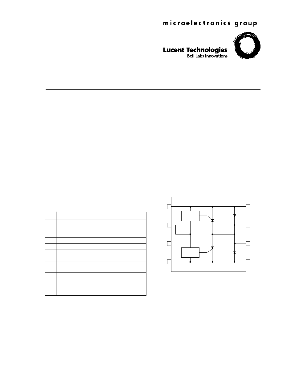
- Figure 1. Functional and Pin Diagram
- Figure 2. Pulse Waveform
- Figure 3. Typical Trip Characteristics of the SLIC Protector
- Figure 4. Standard Configuration
- Figure 5. Test Configuration
- Figure 6. Fully Protected Electronic TIP-RING Interface
- Contact Us
Data Sheet
October 1997
L7591 Subscriber Line Interface Circuit Protector
Features
s
Shunts lightning pulses to ground
-- Positive or negative 30 A, 10 x 1000
µ
s
-- Positive or negative 40 A, 5 x 320
µ
s
-- Positive or negative 80 A, 2 x 10
µ
s
s
Power-cross protection
-- 3.5 A
PEAK
, 50 Hz to 60 Hz, 1 s
-- 5.0 A
PEAK
, 50 Hz to 60 Hz, 10 ms
s
Gate trigger current, 15 mA max
s
Up to ≠80 V capability
s
Holding current, 150 mA min
Pin Information
Table 1. Pin Description
(Applies to DIP and SONB packages)
Note: Pins 1 and 4 must always be connected to the protection
resistors shown in Figures 4 and 5 (Line Feed Circuitry). The
SLIC can be connected either to the protected outputs (pins
5 and 8) or to the inputs (pins 1 and 4).
Description
The L7591 Subscriber Line Interface Circuit (SLIC)
Protector is designed to protect line-feed circuitry
from fault-induced lightning and power-cross surge
pulses. If a fault current forces TIP and/or RING to a
more negative voltage than V
S
, current is conducted
through the trip circuit. When the specified trip cur-
rent level is reached, transistors PNPN1 and/or
PNPN2 will turn on and "crowbar" the majority of the
current to ground. If similar pulses force TIP and/or
RING to a more positive state than ground, diodes
D1 and/or D2 will conduct the pulse to ground. The
L7591 SLIC Protector is available in an 8-pin, plastic
DIP (L7591AB) and in an 8-pin, plastic SONB pack-
age (L7591AS).
12-1590 (C)
Figure 1. Functional and Pin Diagram
Pin
Symbol
Name/Function
1
TIP
Tip signal from customer.
2
V
S
Supply voltage to gate
(≠20 V to ≠80 V).
3
--
Test Point, do not use.
4
RING
Ring signal from customer.
5
PR
Protected ring signal to line-feed-
circuitry.
6
GND
Device ground/fault current
return.
7
GND
Device ground/fault current
return.
8
PT
Protected tip signal to line-feed
circuitry.
1
2
3
4
8
7
6
5
TIP
V
S
TEST
POINT
RING
PT
GND
GND
PR
PNPN1
PNPN2
D1
D2
TRIP
CIRCUIT
TRIP
CIRCUIT
2
Lucent Technologies Inc.
Data Sheet
October 1997
L7591 Subscriber Line Interface Circuit Protector
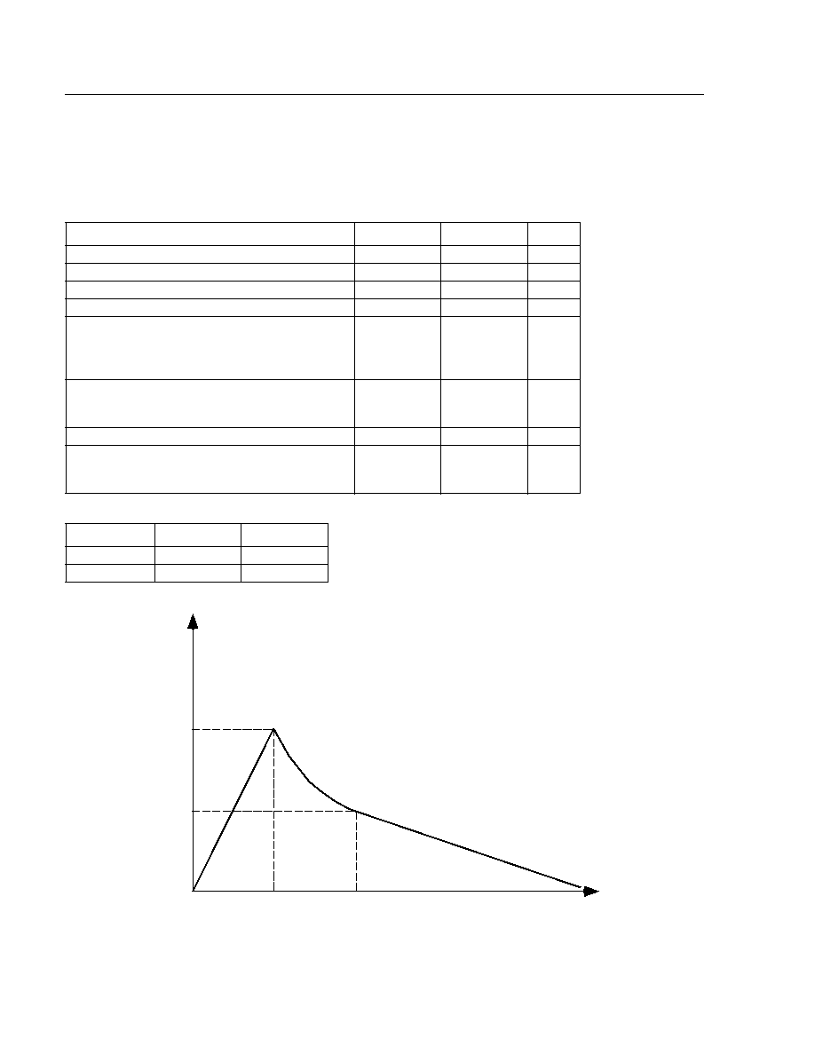
Absolute Maximum Ratings
(At 25
∞
C)
Stresses in excess of the Absolute Maximum Ratings can cause permanent damage to the device. These are
absolute stress ratings only. Functional operation of the device is not implied at these or any other conditions in
excess of those given in the operational sections of the data sheet. Exposure to Absolute Maximum Ratings for
extended periods can adversely affect the device reliability.
*Pulse Waveform Data:
Figure 2. Pulse Waveform
Parameter
Symbol
Value
Unit
Ambient Operating Temperature
T
A
≠40 to +85
∞
C
Storage Temperature Range
T
stg
≠40 to +125
∞
C
Pin Soldering Temperature (t = 15 s max)
--
300
∞
C
Supply Voltage
V
S
≠83
V
Peak Pulse Current: * (See Figure 2.)
10 x 1000
µ
s
5 x 320
µ
s
2 x 10
µ
s
--
--
--
30
40
80
A
A
A
Nonrepetitive Peak ON-state Current:
t = 1 s, f = 50 Hz to 60 Hz
t = 10 ms, f = 50 Hz to 60 Hz
--
--
3.5
5
A
A
Maximum Gate Current (Half Sine Wave 10 ms)
--
2
A
Maximum Voltage:
TIP or RING to Gnd
V
S
to Gnd
--
--
≠100
≠80
V
V
10 x 1000
µ
s
tr = 10
µ
s
tp = 1000
µ
s
5 x 320
µ
s
tr = 5
µ
s
tp = 320
µ
s
2 x 10
µ
s
tr = 2
µ
s
tp = 10
µ
s
% IPP
100
50
0
tr
tp
t
Lucent Technologies Inc.
3
Data Sheet
October 1997
L7591 Subscriber Line Interface Circuit Protector
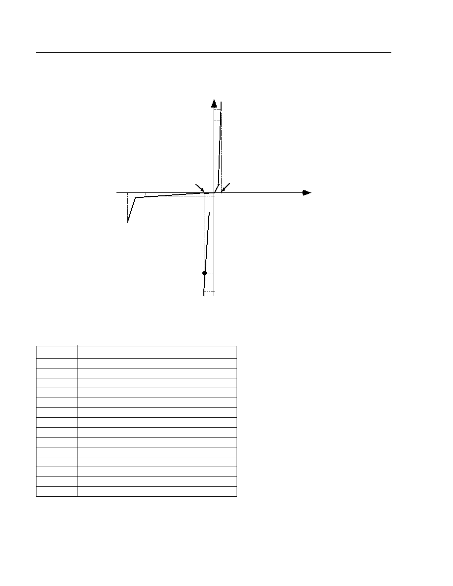
Electrical Specifications
(T
A
= 25
∞
C)
The minimum and/or maximum limits specified for the parameters are based on the absolute system. The alge-
braic sign only applies to the direction of the parameter. These requirements apply to either the TIP or RING termi-
nal; however, the device is capable of simultaneous Tip and Ring surges and continuous current, as noted below in
Tip and Ring leads. See Figure 3 and Table 5 for symbol and test condition definition.
Table 2. Electrical Characteristics D1 and D2
Table 3. Electrical Characteristics, PNPN Circuitry
Table 4. Electrical Characteristics, Diode and PNPN Circuitry
Characteristic
Symbol
Test Conditions
Min
Typ
Max
Unit
Forward Voltage
V
F
I
P
= 5 A, t
P
= 1 ms
--
1.6
3
V
Peak Forward Voltage
V
FP
I
PP
= 30 A, 10 x 1000
µ
s
--
5.2
15
V
Characteristic
Symbol
Test Conditions
Min
Typ
Max
Unit
Gate Trigger Current
I
GT
V
S
= 48 V
0.2
--
15
mA
Holding Current
I
H
t
P
= 10 ms, V
S
= 48 V
≠150
≠250
--
mA
Trip Voltage
V
T
dc
--
V
S
≠2.0
V
S
≠2.8
V
Dynamic Trip Voltage
V
SGL
I
PP
= 30 A, V
S
= ≠48 V,
10 x 1000
µ
s
--
≠51
≠63
V
Reverse Leakage Current:
V
S
to Tip or Ring
T
A
= 25
∞
C
T
A
= 70
∞
C
I
RG
--
--
V
S
= ≠75 V
--
--
--
--
0.12
--
5
50
µ
A
µ
A
dv/dt Sensitivity
--
Tip or Ring Lead
±
1000
--
--
V/
µ
s
On-state Voltage:
V
ON
t
P
= 1 ms
I
T
= 0.5 A
--
--
--
≠1.3
--
V
I
T
= 3.0 A
--
--
--
≠2.3
--
V
Characteristic
Symbol
Test Conditions
Min
Typ
Max
Unit
Reverse Leakage Current:
(Gate Open)
T
A
= 25
∞
C
T
A
= 70
∞
C
I
R
--
--
V
R
= ≠85 V
--
--
--
--
0.14
--
5
50
µ
A
µ
A
Off-state Capacitance:
V
R
= ≠3 V
V
R
= ≠48 V
C
off
--
--
f = 1 MHz
--
--
--
--
50
40
--
--
pF
pF
4
Lucent Technologies Inc.
Data Sheet
October 1997
L7591 Subscriber Line Interface Circuit Protector
Characteristic Curves
Figure 3. Typical Trip Characteristics of the SLIC Protector
Table 5. Symbols Definition
Symbol
Parameter
I
H
PNPN holding current
I
GT
Gate trigger current out of pin V
S
I
P
Pulse current
I
PP
Peak pulse current
I
RG
Reverse leakage current V
S
to Tip or Ring
I
T
Tip or Ring current when PNPN is on
I
R
Reverse leakage current, Tip or Ring to Ground
V
F
Forward voltage, Tip or Ring to Ground
V
FP
Peak forward voltage, Tip or Ring to Ground
V
T
Trip voltage, Tip or Ring to V
S
V
SGL
Dynamic trip voltage, Tip or Ring to V
S
V
ON
PNPN on voltage at I
T
V
R
Tip or Ring voltage when PNPN is off
C
off
Off-state capacitance, Tip or Ring to Ground
I
I
P
I
PP
V
ON
V
F
I
R
I
H
V
SGL
V
R
V
I
PP
I
T

Lucent Technologies Inc.
5
Data Sheet
October 1997
L7591 Subscriber Line Interface Circuit Protector
Applications
12-1632 (C)
R
PT
and R
PR
must be properly selected for proper operation and/or response.
Figure 4. Standard Configuration
12-1596 (C)
Figure 5. Test Circuit
12-1598 (C)
*An example device is Lucent Technologies Microelectronics Group's LB1276 High Balance SLIC.
Figure 6. Fully Protected Electronic TIP-RING Interface (Not all devices needed in all applications)
1
2
3
4
8
7
6
5
TRIP
CIRCUIT
TRIP
CIRCUIT
≠V
S
PROTECTED
TIP
PROTECTED
RING
TIP
RING
R
PT
R
PR
1
2
3
4
8
7
6
5
TRIP
CIRCUIT
TRIP
CIRCUIT
I
P
I
P
≠48 V
V
MEAS
V
MEAS
BATTERY
FEED*
1
6
7
4
8
2
5
V
S
(≠20 V TO ≠80 V)
PTC
CARBON
BLOCK
CARBON
BLOCK
TIP
RING
PTC
RELAYS
L7591AB
SLIC
PROTECTOR

6
Lucent Technologies Inc.
Data Sheet
October 1997
L7591 Subscriber Line Interface Circuit Protector
Outline Drawings
8-Pin DIP (L7591AB)
Dimensions are in millimeters.
5-4410r.1
Package
Description
Number of
Pins
(N)
Package Dimensions
Maximum Length
(L)
Maximum Width
Without Leads
(B)
Maximum Width
Including Leads
(W)
Maximum Height
Above Board
(H)
PDIP3 (Plastic
Dual-In-Line
Package)
8
10.16
6.48
7.87
5.46
W
H
0.023 MAX
2.54 TYP
0.38 MIN
SEATING PLANE
N
1
PIN #1 IDENTIFIER ZONE
L
B

Lucent Technologies Inc.
7
Data Sheet
October 1997
L7591 Subscriber Line Interface Circuit Protector
Outline Drawings
(continued)
8-Pin, SONB (L7591AS)
Dimensions are in millimeters.
5-4414r.2
Package
Description
Number of
Pins
(N)
Package Dimensions
Maximum Length
(L)
Maximum Width
Without Leads
(B)
Maximum Width
Including Leads
(W)
Maximum Height
Above Board
(H)
SONB (Small
Outline, Narrow
Body)
8
5.08
4.01
6.17
1.73
W
0.024
0.020 MAX
H
0.36 MIN
0.10
SEATING PLANE
1.27 TYP
N
L
B
1
PIN #1 IDENTIFIER ZONE

Data Sheet
October 1997
L7591 Subscriber Line Interface Circuit Protector
For additional information, contact your Microelectronics Group Account Manager or the following:
INTERNET:
http://www.lucent.com/micro
E-MAIL:
docmaster@micro.lucent.com
U.S.A.:
Microelectronics Group, Lucent Technologies Inc., 555 Union Boulevard, Room 30L-15P-BA, Allentown, PA 18103
1-800-372-2447, FAX 610-712-4106 (In CANADA: 1-800-553-2448, FAX 610-712-4106)
ASIA PACIFIC: Microelectronics Group, Lucent Technologies Singapore Pte. Ltd., 77 Science Park Drive, #03-18 Cintech III, Singapore 118256
Tel. (65) 778 8833, FAX (65) 777 7495
JAPAN:
Microelectronics Group, Lucent Technologies Japan Ltd., 7-18, Higashi-Gotanda 2-chome, Shinagawa-ku, Tokyo 141, Japan
Tel. (81) 3 5421 1600, FAX (81) 3 5421 1700
EUROPE:
Data Requests: MICROELECTRONICS GROUP DATALINE: Tel. (44) 1189 324 299, FAX (44) 1189 328 148
Technical Inquiries: GERMANY: (49) 89 95086 0 (Munich), UNITED KINGDOM: (44) 1344 865 900 (Bracknell),
FRANCE: (33) 1 41 45 77 00 (Paris), SWEDEN: (46) 8 600 7070 (Stockholm), FINLAND: (358) 9 4354 2800 (Helsinki),
ITALY: (39) 2 6601 1800 (Milan), SPAIN: (34) 1 807 1441 (Madrid)
Lucent Technologies Inc. reserves the right to make changes to the product(s) or information contained herein without notice. No liability is assumed as a result of their use or application. No
rights under any patent accompany the sale of any such product(s) or information.
Copyright © 1997 Lucent Technologies Inc.
All Rights Reserved
Printed in U.S.A.
October 1997
DS98-034ALC (Replaces DS97-158ALC)
Printed On
Recycled Paper
Ordering Information
Device Part No.
Description
Package
Comcode
ATTL7591AB
SLIC Protector
8-Pin DIP
107056582
ATTL7591AS
SLIC Protector
8-Pin SONB
107056590
ATTL7591AS-TR
SLIC Protector
8-Pin SONB (Tape and Reel)
107232787