 | –≠–Ľ–Ķ–ļ—ā—Ä–ĺ–Ĺ–Ĺ—č–Ļ –ļ–ĺ–ľ–Ņ–ĺ–Ĺ–Ķ–Ĺ—ā: ACT8504 | –°–ļ–į—á–į—ā—Ć:  PDF PDF  ZIP ZIP |
eroflex Circuit T
echnology
≠ Multiplexer Modules For The Future © SCD8504 REV A 10/26/01
Features
Radiation Environment
∑ Radiation 300K(Si) Total Dose
∑
No Latch-Up
or SEE to 120MeV/cm
2
/mg
Full Military Temperature Range
Low Power Consumption < 75mW
64 Channels Provided by Four (4) HS-1840RH Multiplexers
Address Bus (A
0-3
)
,
and Four Enable lines afford flexible organization
Output Monitoring of HS-1840RH outputs to a Fifth HS1840RH. Controlled with
C
0,
C
1
Address Lines.
All Channel Inputs protected by Ī20V Transorbs
Fast Access Time 1500ns
Ī35V Input Over Voltage Protection (Power On or Off)
Break-Before-Make Switching
High Analog Input Impedance (Power On or Off)
Dielectrically Isolated Device Islands
No Latch-Up
Packaging ≠ Hermetic Ceramic Quad Flat Pack
∑ 96 Leads, 1.32"Sq x .20"Ht Quad Flat Pack
∑ Typical Weight 15 grams
DESC SMD Pending
General Description
Aeroflex's ACT8504 is a radiation hardened, multi-chip 64 channel multiplexer MCM (multi-chip
module) with ESD protection for use in space applications. All channel inputs have electrostatic
discharge protection.
The ACT8504 has been specifically designed to meet exposure to radiation environments. The
multiplexer is available in a 96 lead High Temperature Co-Fired Ceramic (HTCC) Quad Flatpack
(QFP) and is guaranteed operational from -55įC to +125įC. Available screened in accordance with
MIL-PRF-38534, the ACT8504 is ideal for demanding military and space applications.
F
I
E
I
D
C
E
R T
A
E
R
O
F
L E
X L A
B
S
I
N
C
.
ISO
9001
CIRCUIT TECHNOLOGY
www.aeroflex.com
ACT8504
Radiation Hardened & ESD Protected
With MUX Output Monitor Function
64-Channel Analog Multiplexer Module
2
Aeroflex Circuit Technology
SCD8504 REV A 10/26/01 Plainview NY (516) 694-6700
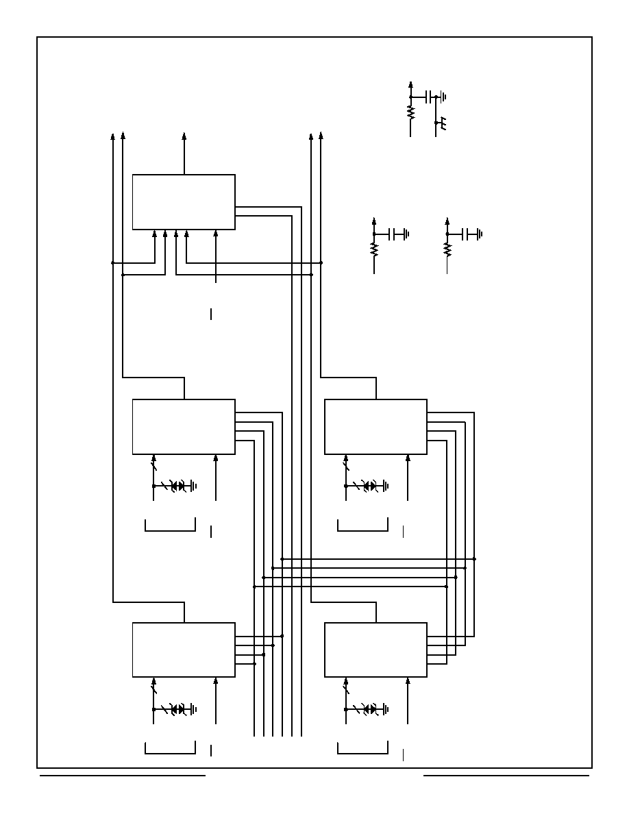
A
C
T
8504
64 C
h
ann
e
l A
n
alog
MU
X
B
l
o
c
k D
i
a
g
r
a
m
CH 0
CH 1
5
∑
∑
∑
EN
0-
15
OUT
P
UT
0
-
1
5
16
VR
+V
CC
-V
EE
V
RE
F
GND
16
CH 1
6
CH 3
1
∑
∑
∑
EN
16
-
3
1
OUT
P
UT
1
6
-
3
1
16
VR
16
OUT
P
UT
M
O
NI
T
O
R
MU
X
CH 3
2
CH 4
7
∑
∑
∑
EN
32
-
4
7
16
VR
16
CH 4
8
CH 6
3
∑
∑
∑
EN
48
-
6
3
OUT
P
UT
4
8
-
6
3
16
VR
16
A0
A1
A2
A3
C0
C1
MU
X
4
MU
X
3
MU
X
2
OUT
P
UT
MO
N
I
T
O
R
MU
X
1
OUT
P
UT
3
2
-
4
7
EN
32
-
4
7

3
Aeroflex Circuit Technology
SCD8504 REV A 10/26/01 Plainview NY (516) 694-6700
Organization and Application
The ACT8504 consists of four 16 channel muxes arranged as shown in the Block Diagram.
The muxes channels 0-63 are controlled by address lines A
0
- A
3
. The mux output monitor is
controlled by address lines C
0
, C
1
.
The ACT8504 design is inherently Radiation Hard due to the HS1840RH Multiplexers as well
as Microsemi Corp. Transient Suppressors (Reference Microsemi MicroNotes Series 050 -
page 14).
NOTE: It is recommended that all "NC or "no connect pin", be grounded. This eliminates or
minimizes any ESD or static buildup.
4
Aeroflex Circuit Technology
SCD8504 REV A 10/26/01 Plainview NY (516) 694-6700
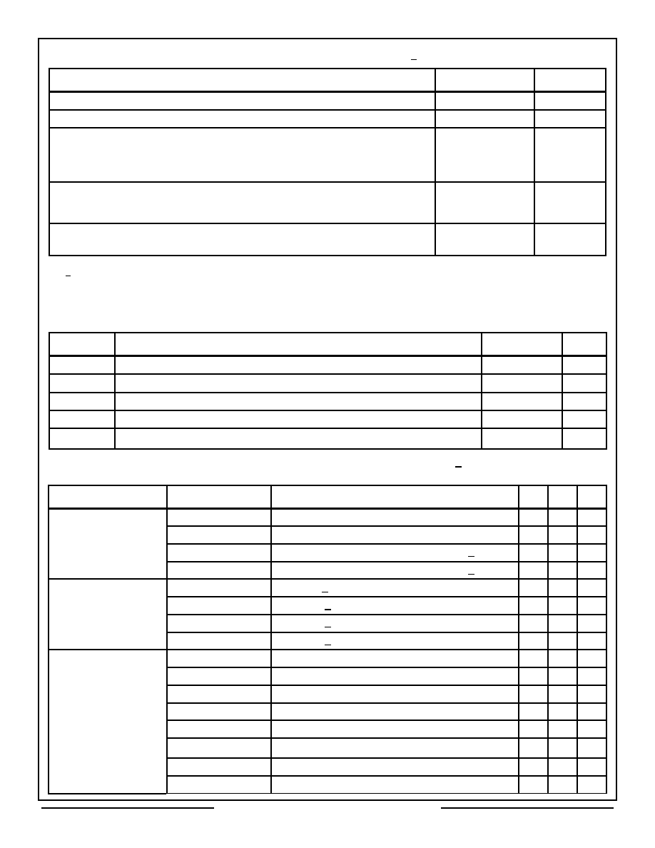
Absolute Maximum Ratings
1/
Parameter
Range
Units
Case Operating Temperature Range
-55 to +125
įC
Storage Temperature Range
-55 to +150
įC
Supply Voltage
+V
CC
(Pin 44)
-V
EE
(Pin 46)
V
REF
(Pin 48)
+20
-20
+20
V
V
V
Digital Input Overvoltage
V
EN
(Pins 5, 6, 91, 92), V
A
(Pins 93, 95, 1, 3), VC (Pins 2, 4)
< V
R
+4
> GND -4
V
V
Analog Input Over Voltage
V
S
Ī18
V
Notes:
1/ All measurements are made with respect to ground.
NOTICE: Stresses above those listed under "Absolute Maximums Rating" may cause permanent damage to the device. These are stress rating
only; functional operation beyond the "Operation Conditions" is not recommended and extended exposure beyond the "Operation
Conditions" may effect device reliability.
Recommended Operating Conditions
Symbol
Parameter
Typical
Units
+V
CC
+15V Power Supply Voltage
+15.0
V
-V
EE
-15V Power Supply Voltage
-15.0
V
V
REF
Reference Voltage
+5.00
V
V
AL
Logic Low Level
+0.8
V
V
AH
Logic High Level
+4.0
V
DC Electrical Performance Characteristics
1/
(Tc = -55įC to +125įC, +V
EE
= +15V, -V
EE
= -15V, V
REF
= +5.0V, Unless otherwise specified)
Parameter
Symbol
Conditions
Min
Max Units
Supply Current
I+
V
EN
(0-63)
= V
A
(0-3)
A
= V
A
(0-1)
C
= 0
.25
2.5
mA
I-
V
EN
(0-63)
= V
A
(0-3)
A
= V
A
(0-1)
C
= 0
-2.5
-.25
mA
+I
SBY
V
EN
(0-63)
= 4V, V
A
(0-3)
A
= V
A
(0-1)
C
= 0 6/
0.25
2.5
mA
-I
SBY
V
EN
(0-63)
= 4V, V
A
(0-3)
A
= V
A
(0-1)
C
= 0 6/
-2.5
0.25
mA
Address Input Current
I
AL
(0-3)
A
V
A
= 0V 1/
-4
4
ĶA
I
AH
(0-3)
A
V
A
= 5V 1/
-4
4
ĶA
I
AL
(0-1)
C
V
A
= 0V 1/
-1
1
ĶA
I
AH
(0-1)
C
V
A
= 5V 1/
-1
1
ĶA
Enable Input Current
I
ENL
(0-15)
V
EN
(0-15)
= 0V
-1
1
ĶA
I
ENH
(0-15)
V
EN
(0-15)
= 5V
-1
1
ĶA
I
ENL
(16-31)
V
EN
(16-31)
= 0V
-1
1
ĶA
I
ENH
(16-31)
V
EN
(16-31)
= 5V
-1
1
ĶA
I
ENL
(32-47),(M
UX
M
ON
)
V
EN
(32-47)
, V
EN
(M
UX
M
ON
)
= 0V
-2
2
ĶA
I
ENH
(32-47),(M
UX
M
ON
)
V
EN
(32-47)
, V
EN
(M
UX
M
ON
)
= 5V
-2
2
ĶA
I
ENL
(48-63)
V
EN
(48-63)
= 0V
-1
1
ĶA
I
ENH
(48-63)
V
EN
(48-63)
= 5V
-1
1
ĶA
5
Aeroflex Circuit Technology
SCD8504 REV A 10/26/01 Plainview NY (516) 694-6700
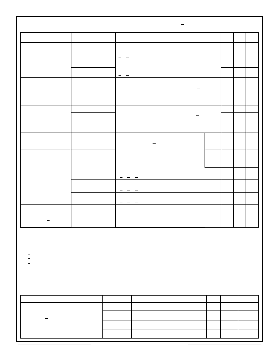
Positive Input
Leakage Current
CH0-CH63
+I
SOFFOUTPUT
(
ALL
)
V
IN
= +10V, V
EN
= 4V, output and all
unused MUX inputs under test = -10V
2/, 3/
-100 +700
nA
+I
SOFFCURRENT
(
ALL
)
-100 +700
nA
Negative Input
Leakage Current
CH0-CH63
-I
SOFFOUTPUT
(
ALL
)
V
IN
= -10V, V
EN
= 4V, output and all
unused MUX inputs under test = +10V
2/, 3/
-100 +700
nA
-I
SOFFCURRENT
(
ALL
)
-100 +700
nA
Output Leakage
Current OUTPUTS
(pins 3,13, 23 & 33)
Mux Monitor
(pin 69)
+I
DOFFOUTPUT
(
ALL
)
V
OUT
= +10V, V
EN
= 4V, output and all
unused MUX inputs under test = -10V 3/,
4/
-100 +100
nA
+I
DOFFCURRENT
(
ALL
)
-100 +100
nA
Output Leakage
Current OUTPUTS
(pins 3,13, 23 & 33)
Mux Monitor
(pin 69)
-I
DOFFOUTPUT
(
ALL
)
V
OUT
= -10V, V
EN
= 4V, output and all
unused MUX inputs under test = +10V 3/,
4/
-100 +100
nA
-I
DOFFCURRENT
(
ALL
)
-100 +100
nA
Input Clamped Voltage
CH0 - CH63
+V
CLMP
(0-63
V
EN
= 4V, all unused MUX inputs under
test are open. 3/
+25įC
+125įC
-55įC
18.0
18.0
17.5
23.0
23.5
22.5
V
V
V
Input Clamped Voltage
CH0 - CH63
-V
CLMP
(0-63
+25įC
+125įC
-55įC
-23.0
-23.5
-22.5
-18.0
-18.0
-17.5
V
V
V
Switch ON Resistance
OUTPUTS
(pins 25, 26, 68 & 70)
R
DS
(
ON
)
(0-63)
A
V
IN
= +15V, V
EN
= 0.8V, I
OUT
= -1mA
2/, 3/, 5/
500 3000
R
DS
(
ON
)
(0-63)
B
V
IN
= +5V, V
EN
= 0.8V, I
OUT
= -1mA
2/, 3/, 5/
500 3000
R
DS
(
ON
)
(0-63)
C
V
IN
= -5V, V
EN
= 0.8V, I
OUT
= +1mA
2/, 3/, 5/
500 3000
Switch ON Resistance
Mux Monitor Only
(pin 69) 6/
R
DS
(
ON
)
(MuxMon)
-
500 3000
Notes:
1/ Measure inputs sequentially. Ground all unused inputs of the MUX under test. VA is the applied input voltage to the MUXes' address lines
A(0-5).
2/ V
IN
is the applied input voltage to the MUXes' input channel CH0-CH63.
3/ V
EN
is the applied input voltage to the MUXes' enable line En(0-15), En(16-31), En(32-47) and En(48-63).
4/ V
OUT
is the applied input voltage to the MUXes' output line OUTPUT(1-15), OUTPUT(16-31), OUTPUT(32-47) and OUTPUT(48-63).
5/ Negative current is the current flowing out of each of the MUX pins. Positive current is the current flowing into each MUX pin.
6/ If not tested, shall be guaranteed to the specified limits.
Switching Characteristics
(Tc = -55įC to +125įC, V
DD
= +15V, V
EE
= -15V, V
R
= +5.0V, Unless otherwise specified)
Parameter
Symbol
Conditions
Min
Max
Units
Switching Test MUX
(For Mux Output Monitor,
See Note 6/)
t
ON
A
R
L
= 10K
, C
L
= 50pF
10
1500
ns
t
OFF
A
R
L
= 10K
, C
L
= 50pF
10
2000
ns
t
ON
EN
R
L
= 1K
, C
L
= 50pF
10
1500
ns
t
OFF
EN
R
L
= 1K
, C
L
= 50pF
10
1000
ns
DC Electrical Performance Characteristics
1/
(con't)
(Tc = -55įC to +125įC, +V
EE
= +15V, -V
EE
= -15V, V
REF
= +5.0V, Unless otherwise specified)
Parameter
Symbol
Conditions
Min
Max Units
6
Aeroflex Circuit Technology
SCD8504 REV A 10/26/01 Plainview NY (516) 694-6700
Truth Table (CH0 ≠ CH15)
A3
A2
A1
A0
EN(0-15)
"ON" CHANNEL
1/
X
X
X
X
H
NONE
L
L
L
L
L
CH0
L
L
L
H
L
CH1
L
L
H
L
L
CH2
L
L
H
H
L
CH3
L
H
L
L
L
CH4
L
H
L
H
L
CH5
L
H
H
L
L
CH6
L
H
H
H
L
CH7
H
L
L
L
L
CH8
H
L
L
H
L
CH9
H
L
H
L
L
CH10
H
L
H
H
L
CH11
H
H
L
L
L
CH12
H
H
L
H
L
CH13
H
H
H
L
L
CH14
H
H
H
H
L
CH15
1/ Between CH0-15 and OUTPUT (0-15)
Truth Table (CH16 ≠ CH31)
A3
A2
A1
A0
EN(16-31)
"ON" CHANNEL
1/
X
X
X
X
H
NONE
L
L
L
L
L
CH16
L
L
L
H
L
CH17
L
L
H
L
L
CH18
L
L
H
H
L
CH19
L
H
L
L
L
CH20
L
H
L
H
L
CH21
L
H
H
L
L
CH22
L
H
H
H
L
CH23
H
L
L
L
L
CH24
H
L
L
H
L
CH25
H
L
H
L
L
CH26
H
L
H
H
L
CH27
H
H
L
L
L
CH28
H
H
L
H
L
CH29
H
H
H
L
L
CH30
H
H
H
H
L
CH31
1/ Between CH16-31 and OUTPUT (16-31)
7
Aeroflex Circuit Technology
SCD8504 REV A 10/26/01 Plainview NY (516) 694-6700
Truth Table (CH32 ≠ CH47)
A3
A2
A1
A0
EN(32-47)
"ON" CHANNEL
1/
X
X
X
X
H
NONE
L
L
L
L
L
CH32
L
L
L
H
L
CH33
L
L
H
L
L
CH34
L
L
H
H
L
CH35
L
H
L
L
L
CH36
L
H
L
H
L
CH37
L
H
H
L
L
CH38
L
H
H
H
L
CH39
H
L
L
L
L
CH40
H
L
L
H
L
CH41
H
L
H
L
L
CH42
H
L
H
H
L
CH43
H
H
L
L
L
CH44
H
H
L
H
L
CH45
H
H
H
L
L
CH46
H
H
H
H
L
CH47
1/ Between CH32-47 and OUTPUT (32-47)
Truth Table (CH48 ≠ CH63)
A3
A2
A1
A0
EN(47-63)
"ON" CHANNEL
1/
X
X
X
X
H
NONE
L
L
L
L
L
CH48
L
L
L
H
L
CH49
L
L
H
L
L
CH50
L
L
H
H
L
CH51
L
H
L
L
L
CH52
L
H
L
H
L
CH53
L
H
H
L
L
CH54
L
H
H
H
L
CH55
H
L
L
L
L
CH56
H
L
L
H
L
CH57
H
L
H
L
L
CH58
H
L
H
H
L
CH59
H
H
L
L
L
CH60
H
H
L
H
L
CH61
H
H
H
L
L
CH62
H
H
H
H
L
CH63
1/ Between CH48-63 and OUTPUT (48-63)
8
Aeroflex Circuit Technology
SCD8504 REV A 10/26/01 Plainview NY (516) 694-6700
Truth Table (Mux Output Monitor)
C1
C0
EN(32-47)
"ON" CHANNEL
X
X
H
NONE
L
L
L
Output Channels 0-15
L
H
L
Output Channels 16-31
H
L
L
Output Channels 32-47
H
H
L
Output Channels 48-63
9
Aeroflex Circuit Technology
SCD8504 REV A 10/26/01 Plainview NY (516) 694-6700
0.8V
Enable Line
4V
OUTPUT
t
ON
EN
t
OFF
EN
Definition of
t
OFF
A
t
OFF
A
0V
OUTPUT
0.8V
4V
t
ON
A
Definition of
t
ON
A
0V
12V MIN
OUTPUT
0.8V
4V
Address Lines
Definition of t
ON
EN
and t
OFF
EN
0V
Address Lines
50%
90%
10%
10
Aeroflex Circuit Technology
SCD8504 REV A 10/26/01 Plainview NY (516) 694-6700
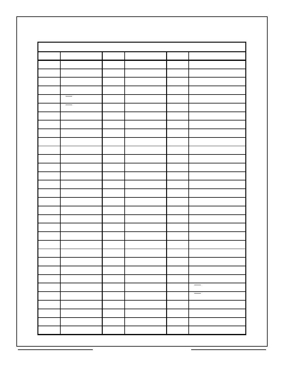
Lead Numbers & Functions
ACT8504 ≠ 96 Leads Ceramic QUAD Flat Pack
Pin #
Function
Pin #
Function
Pin #
Function
1
A
2
33
CH11
65
CH49
2
C
0
34
CH27
66
CH48
3
A
3
35
CH12
67
NC
4
C
1
36
CH28
68
Output V(48-63)
5
EN 0-15
37
CH13
69
Mux Output Monitor
6
EN 16-31
38
CH29
70
Output V(32-47)
7
CH0
39
CH14
71
GND
8
CH16
40
CH30
72
GND
9
CH1
41
CH15
73
CH47
10
CH17
42
CH31
74
CH46
11
CH2
43
NC
75
CH45
12
CH18
44
+V
CC
76
CH44
13
CH3
45
NC
77
CH43
14
CH19
46
-V
EE
78
CH42
15
CH4
47
NC
79
CH41
16
CH20
48
V
REF
80
CH40
17
CH5
49
NC
81
CH39
18
CH21
50
CASE GND
82
CH38
19
CH6
51
CH63
83
CH37
20
CH22
52
CH62
84
CH36
21
CH7
53
CH61
85
CH35
22
CH23
54
CH60
86
CH34
23
GND
55
CH59
87
CH33
24
GND
56
CH58
88
CH32
25
Output V(0-15)
57
CH57
89
GND
26
Output V(16-31)
58
CH56
90
GND
27
CH8
59
CH55
91
EN 48-63
28
CH24
60
CH54
92
EN 32-47
29
CH9
61
CH53
93
A
0
30
CH25
62
CH52
94
NC
31
CH10
63
CH51
95
A
1
32
CH26
64
CH50
96
NC
NOTE: It is recommended that all "NC or "no connect pin", be grounded. This eliminates or minimizes any ESD or static buildup.
11
Aeroflex Circuit Technology
SCD8504 REV A 10/26/01 Plainview NY (516) 694-6700
C I R C U I T T E C H N O L O G Y
Ordering Information
Model Number
Screening
DESC SMD #
Package
ACT8504 -S
Military Temperature, -55įC to +125įC,
Screened to the individual test methods of MIL-STD-883 IAW
MIL-PRF-38534 Class K
Pending
QUAD Flat
Pack
ACT8504
Military Temperature, -55įC to +125įC,
Screened to the individual test methods of MIL-STD-883 IAW
MIL-PRF-38534 Class H
ACT8504 -7
Commercial Flow, +25įC testing only
NA
ACT8504 -T
Commercial Flow, -55įC to +125įC testing only
ACT8504 -I
Commercial Flow, -40įC to +85įC testing only
ACT8504 -C
Commercial Flow, -0įC to +70įC testing only
Specifications subject to change without notice
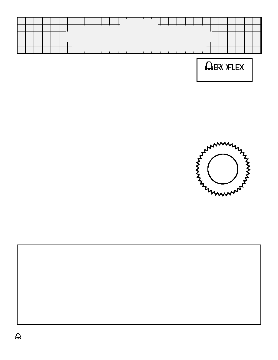
1.320 SQ
Pin 85
Pin 12
Pin 60
Pin 37
Pin 13
Pin 36
Pin 61
Pin 84
Pin 1
Flat Package Outline
MAX
(23 Spaces at .050)
Tol Non-Cum
4 Sides
.0165
Ī.003
1.150 Ī.005
.200
MAX
(.400)
Note: Outside ceramic tie
bars not shown for clarity.
Contact factory for details
.006
Ī.001
Aeroflex Circuit Technology
35 South Service Road
Plainview New York 11803
Telephone: (516) 694-6700
FAX: (516) 694-6715
Toll Free Inquiries: (800) THE-1553
www.aeroflex.com
E-Mail: sales-act@aeroflex.com