 | ÐлекÑÑоннÑй компоненÑ: ADXL250 | СкаÑаÑÑ:  PDF PDF  ZIP ZIP |
Äîêóìåíòàöèÿ è îïèñàíèÿ www.docs.chipfind.ru
FUNCTIONAL BLOCK DIAGRAMS
SELF-TEST
+V
S
2
25k
5k
ADXL150
GAIN
AMP
OFFSET
NULL
COM
0.1 F
BUFFER
AMP
DEMODULATOR
SENSOR
+V
S
TP
(DO NOT CONNECT)
V
OUT
9
CLOCK
SELF-TEST
5k
25k
ADXL250
GAIN
AMP
Y OFFSET
NULL
COM
0.1 F
BUFFER
AMP
DEMODULATOR
+V
S
TP
(DO NOT CONNECT)
25k
5k
GAIN
AMP
BUFFER
AMP
DEMODULATOR
V
OUT
Y
X OFFSET
NULL
SENSOR
+V
S
2
CLOCK
SENSOR
V
OUT
X
a
5
g to 50 g, Low Noise, Low Power,
Single/Dual Axis i
MEM
S
®
Accelerometers
ADXL150/ADXL250
GENERAL DESCRIPTION
The ADXL150 and ADXL250 are third generation
±
50 g sur-
face micromachined accelerometers. These improved replace-
ments for the ADXL50 offer lower noise, wider dynamic range,
reduced power consumption and improved zero g bias drift.
The ADXL150 is a single axis product; the ADXL250 is a fully
integrated dual axis accelerometer with signal conditioning on a
single monolithic IC, the first of its kind available on the com-
mercial market. The two sensitive axes of the ADXL250 are
orthogonal (90
°
) to each other. Both devices have their sensitive
axes in the same plane as the silicon chip.
The ADXL150/ADXL250 offer lower noise and improved
signal-to-noise ratio over the ADXL50. Typical S/N is 80 dB,
allowing resolution of signals as low as 10 mg, yet still providing
a
±
50 g full-scale range. Device scale factor can be increased
from 38 mV/g to 76 mV/g by connecting a jumper between
V
OUT
and the offset null pin. Zero g drift has been reduced to
0.4 g over the industrial temperature range, a 10
×
improvement
over the ADXL50. Power consumption is a modest 1.8 mA
per axis. The scale factor and zero g output level are both
FEATURES
Complete Acceleration Measurement System
on a Single Monolithic IC
80 dB Dynamic Range
Pin Programmable
50 g or 25 g Full Scale
Low Noise: 1 m
g/
Hz Typical
Low Power: <2 mA per Axis
Supply Voltages as Low as 4 V
2-Pole Filter On-Chip
Ratiometric Operation
Complete Mechanical & Electrical Self-Test
Dual & Single Axis Versions Available
Surface Mount Package
REV. 0
Information furnished by Analog Devices is believed to be accurate and
reliable. However, no responsibility is assumed by Analog Devices for its
use, nor for any infringements of patents or other rights of third parties
which may result from its use. No license is granted by implication or
otherwise under any patent or patent rights of Analog Devices.
ratiometric to the power supply, eliminating the need for a volt-
age reference when driving ratiometric A/D converters such as
those found in most microprocessors. A power supply bypass
capacitor is the only external component needed for normal
operation.
The ADXL150/ADXL250 are available in a hermetic 14-lead
surface mount cerpac package specified over the 0
°
C to +70
°
C
commercial and 40
°
C to +85
°
C industrial temperature ranges.
Contact factory for availability of devices specified over automo-
tive and military temperature ranges.
One Technology Way, P.O. Box 9106, Norwood, MA 02062-9106, U.S.A.
Tel: 781/329-4700
World Wide Web Site: http://www.analog.com
Fax: 781/326-8703
© Analog Devices, Inc., 1998
i
MEM
S
is a registered trademark of Analog Devices, Inc.

2
REV. 0
ADXL150JQC/AQC
ADXL250JQC/AQC
Parameter
Conditions
Min
Typ
Max
Min
Typ Max
Units
SENSOR
Guaranteed Full-Scale Range
±
40
±
50
±
40
±
50
g
Nonlinearity
0.2
0.2
% of FS
Package Alignment Error
1
±
1
±
1
Degrees
Sensor-to-Sensor Alignment Error
±
0.1
Degrees
Transverse Sensitivity
2
±
2
±
2
%
SENSITIVITY
Sensitivity (Ratiometric)
3
Y Channel
33.0
38.0 43.0
mV/g
X Channel
33.0
38.0
43.0
33.0
38.0 43.0
mV/g
Sensitivity Drift Due to Temperature Delta from 25
°
C to T
MIN
or T
MAX
±
0.5
±
0.5
%
ZERO g BIAS LEVEL
Output Bias Voltage
4
V
S
/2 0.35 V
S
/2
V
S
/2 + 0.35 V
S
/2 0.35 V
S
/2 V
S
/2 + 0.35 V
Zero g Drift Due to Temperature
Delta from 25
°
C to T
MIN
or T
MAX
0.2
0.3
g
ZERO-g OFFSET ADJUSTMENT
Voltage Gain
Delta V
OUT
/Delta V
OS PIN
0.45
0.50
0.55
0.45
0.50 0.55
V/V
Input Impedance
20
30
20
30
k
NOISE PERFORMANCE
Noise Density
5
1
2.5
1
2.5
mg/
Hz
Clock Noise
5
5
mV p-p
FREQUENCY RESPONSE
3 dB Bandwidth
900
1000
900
1000
Hz
Bandwidth Temperature Drift
T
MIN
to T
MAX
50
50
Hz
Sensor Resonant Frequency
Q = 5
24
24
kHz
SELF-TEST
Output Change
6
ST Pin from Logic "0" to "1"
0.25
0.40
0.60
0.25
0.40 0.60
V
Logic "1" Voltage
V
S
1
V
S
1
V
Logic "0" Voltage
1.0
1.0
V
Input Resistance
To Common
30
50
30
50
k
OUTPUT AMPLIFIER
Output Voltage Swing
I
OUT
=
±
100
µ
A
0.25
V
S
0.25
0.25
V
S
0.25
V
Capacitive Load Drive
1000
1000
pF
POWER SUPPLY (V
S
)
7
Functional Voltage Range
4.0
6.0
4.0
6.0
V
Quiescent Supply Current
ADXL150
1.8
3.0
mA
ADXL250 (Total 2 Channels)
3.5
5.0
mA
TEMPERATURE RANGE
Operating Range J
0
+70
0
+70
°
C
Specified Performance A
40
+85
40
+85
°
C
NOTES
1
Alignment error is specified as the angle between the true axis of sensitivity and the edge of the package.
2
Transverse sensitivity is measured with an applied acceleration that is 90 degrees from the indicated axis of sensitivity.
3
Ratiometric: V
OUT
= V
S
/2 + (Sensitivity
×
V
S
/5 V
×
a) where a = applied acceleration in gs, and V
S
= supply voltage. See Figure 21. Output scale factor can be
doubled by connecting V
OUT
to the offset null pin.
4
Ratiometric, proportional to V
S
/2. See Figure 21.
5
See Figure 11 and Device Bandwidth vs. Resolution section.
6
Self-test output varies with supply voltage.
7
When using ADXL250, both Pins 13 and 14 must be connected to the supply for the device to function.
Specifications subject to change without notice.
ADXL150/ADXL250SPECIFICATIONS
(T
A
= +25 C for J Grade, T
A
= 40 C to +85 C for A Grade,
V
S
= +5.00 V, Acceleration = Zero
g, unless otherwise noted)
ADXL150/ADXL250
3
REV. 0
Package Characteristics
Package
JA
JC
Device Weight
14-Lead Cerpac
110
°
C/W
30
°
C/W
5 Grams
ORDERING GUIDE
Model
Temperature Range
ADXL150JQC
0
°
C to +70
°
C
ADXL150AQC
40
°
C to +85
°
C
ADXL250JQC
0
°
C to +70
°
C
ADXL250AQC
40
°
C to +85
°
C
ABSOLUTE MAXIMUM RATINGS*
Acceleration (Any Axis, Unpowered for 0.5 ms) . . . . . . 2000 g
Acceleration (Any Axis, Powered for 0.5 ms) . . . . . . . . . 500 g
+V
S
. . . . . . . . . . . . . . . . . . . . . . . . . . . . . . . . 0.3 V to +7.0 V
Output Short Circuit Duration
(V
OUT
, V
REF
Terminals to Common) . . . . . . . . . . . Indefinite
Operating Temperature . . . . . . . . . . . . . . . . . 55
°
C to +125
°
C
Storage Temperature . . . . . . . . . . . . . . . . . . . 65
°
C to +150
°
C
*Stresses above those listed under Absolute Maximum Ratings may cause perma-
nent damage to the device. This is a stress rating only; the functional operation of
the device at these or any other conditions above those indicated in the operational
sections of this specification is not implied. Exposure to absolute maximum rating
conditions for extended periods may affect device reliability.
Drops onto hard surfaces can cause shocks of greater than 2000 g
and exceed the absolute maximum rating of the device. Care
should be exercised in handling to avoid damage.
PIN CONNECTIONS
TOP VIEW
(Not to Scale)
ADXL150
14
1
7
8
NC
NC
NC
NC
NC
COMMON
V
S
NC
NC
V
OUT
SELF-TEST
ZERO
g ADJ
TP (DO NOT CONNECT)
NC = NO CONNECT
ZERO
g ADJ Y
V
OUT
Y
NC
NC
COMMON
V
S
V
S
NC
NC
ZERO
g ADJ X
SELF-TEST
V
OUT
X
TOP VIEW
(Not to Scale)
ADXL250
14
1
7
8
NC
TP (DO NOT CONNECT)
NOTE: WHEN USING ADXL250, BOTH PINS 13 AND 14 NEED
TO BE CONNECTED TO SUPPLY FOR DEVICE TO FUNCTION
NC
POSITIVE A = POSITIVE V
OUT
POSITIVE A = POSITIVE V
OUT
TOP VIEW
(Not to Scale)
ADXL150
14
1
7
8
A
X
TOP VIEW
(Not to Scale)
ADXL250
14
1
7
8
90
A
Y
A
X
Figure 1. ADXL150 and ADXL250 Sensitive Axis
Orientation
CAUTION
ESD (electrostatic discharge) sensitive device. Electrostatic charges as high as 4000 V readily
accumulate on the human body and test equipment and can discharge without detection.
Although the ADXL150/ADXL250 feature proprietary ESD protection circuitry, permanent
damage may occur on devices subjected to high energy electrostatic discharges. Therefore, pro per
ESD precautions are recommended to avoid performance degradation or loss of function ality.
WARNING!
ESD SENSITIVE DEVICE
4
ADXL150/ADXL250
REV. 0
Zero g Bias Level: The output voltage of the ADXL150/
ADXL250 when there is no acceleration (or gravity) acting
upon the axis of sensitivity. The output offset is the difference
between the actual zero g bias level and (V
S
/2).
Polarity of the Acceleration Output
The polarity of the ADXL150/ADXL250 output is shown in
Figure 1. When its sensitive axis is oriented to the earth's gravity
(and held in place), it will experience an acceleration of +1 g.
This corresponds to a change of approximately +38 mV at the
output pin. Note that the polarity will be reversed if the package
is rotated 180
°
. The figure shows the ADXL250 oriented so that
its "X" axis measures +1 g. If the package is rotated 90
°
clock-
wise (Pin 14 up, Pin 1 down), the ADXL250's "Y" axis will now
measure +1 g.
14
1
7
8
A
X
ADXL150
14
1
7
8
A
X
ADXL250
A
Y
Figure 2. Output Polarity
Acceleration Vectors
The ADXL150/ADXL250 is a sensor designed to measure
accelerations that result from an applied force. It responds to
the component of acceleration on its sensitive X axis (ADXL150)
or on both the "X" and "Y" axis (ADXL250).
GLOSSARY OF TERMS
Acceleration: Change in velocity per unit time.
Acceleration Vector: Vector describing the net acceleration
acting upon the ADXL150/ADXL250.
g: A unit of acceleration equal to the average force of gravity
occurring at the earth's surface. A g is approximately equal to
32.17 feet/s
2
or 9.807 meters/s
2
.
Nonlinearity: The maximum deviation of the ADXL150/
ADXL250 output voltage from a best fit straight line fitted to a
plot of acceleration vs. output voltage, calculated as a % of the
full-scale output voltage (at 50 g).
Resonant Frequency: The natural frequency of vibration of
the ADXL150/ADXL250 sensor's central plate (or "beam"). At
its resonant frequency of 24 kHz, the ADXL150/ADXL250's
moving center plate has a slight peak in its frequency response.
Sensitivity: The output voltage change per g unit of accelera-
tion applied, specified at the V
OUT
pin in mV/g.
Total Alignment Error: Net misalignment of the ADXL150/
ADXL250's on-chip sensor and the measurement axis of the
application. This error includes errors due to sensor die align-
ment to the package, and any misalignment due to installation
of the sensor package in a circuit board or module.
Transverse Acceleration: Any acceleration applied 90
°
to the
axis of sensitivity.
Transverse Sensitivity Error: The percent of a transverse
acceleration that appears at V
OUT
.
Transverse Axis: The axis perpendicular (90
°
) to the axis of
sensitivity.
ADXL150/ADXL250
5
REV. 0
4.0
4.5
5.0
5.5
6.0
POWER SUPPLY VOLTAGE
ERROR FROM IDEAL %
5.0
4.0
3.0
2.0
1.0
0
1.0
2.0
3.0
4.0
5.0
Figure 3. Typical Sensitivity Error from Ideal Ratiometric
Response for a Number of Units
4.0
4.5
5.0
5.5
6.0
SUPPLY VOLTAGE
ERROR %
2.5
2.0
1.5
1.0
0.5
0
0.5
1.0
1.5
2.0
Figure 4. Offset Error of Zero g Level from Ideal
V
S
/2 Response as a Percent of Full-Scale for a Number
of Units
SUPPLY VOLTAGE Volts
2.4
2.2
1.2
2
1.8
1.6
1.4
4
6
4.5
SUPPLY CURRENT mA
5
5.5
+105 C
+25 C
40 C
Figure 5. Typical Supply Current vs. Supply Voltage
FREQUENCY Hz
6
100
1k
TYPICAL OUTPUT RESPONSE IN dB
10k
0
6
12
18
24
30
36
42
48
PACKAGE
RESONANCE
BEAM
RESONANCE
Figure 6. Typical Output Response vs. Frequency of
ADXL150/ADXL250 on a PC Board that Has Been
Conformally Coated
0
50
40
80 90 100
TEMPERATURE C
40 30 20 10
10 20
30
60
20
10
0
10
20
70
30
30
ZERO
g
DRIFT mV
Figure 7. Typical Zero g Drift for a Number of Units
TIME 0.2ms/Div
OUTPUT RESPONSE
500
g INPUT
600
g
500
g
400
g
300
g
200
g
100
g
0
g
60
g
50
g
40
g
30
g
20
g
10
g
0
g
Figure 8. Typical 500 g Step Recovery at the Output
Typical Characteristics
(@+5 V dc, +25 C with a 38 mV/
g Scale Factor unless otherwise noted)
6
ADXL150/ADXL250
REV. 0
TIME s
20
0
2
4
6
8
10
12
14
16
18
20
15
10
5
0
5
10
15
ZERO
g
OUTPUT VOLTAGE mV
20
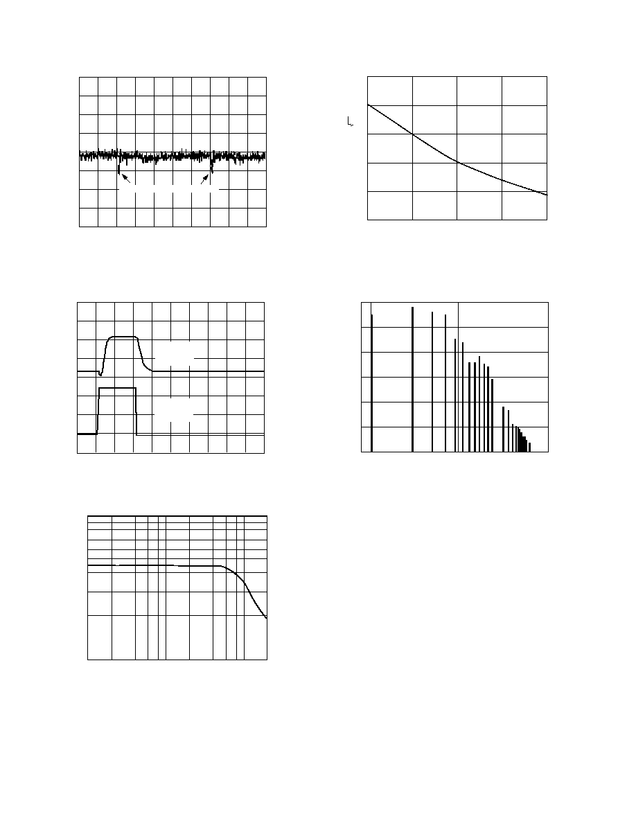
NOISE FROM INTERNAL CLOCK
Figure 9. Typical Output Noise Voltage with Spikes
Generated by Internal Clock
TIME ms
SELF-TEST
OUTPUT
(0.2V/DIV)
SELF-TEST
INPUT
(2V/DIV)
0
2
4
6
8
10
12
14
16
18
20
Figure 10. Typical Self-Test Response
FREQUENCY Hz
2.00
1.75
0.25
2k
10
100
1k
1.50
1.25
0.75
0.50
1.00
2.25
2.50
NOISE m
g
rms
Figure 11. Noise Spectral Density
SUPPLY VOLTAGE Volts
0.6
0.8
4.0
5.0
1.0
1.2
1.4
1.6
4.5
5.5
6.0
RMS NOISE m
g
/
Hz
Figure 12. Noise vs. Supply Voltage
FREQUENCY kHz
30
25
0
100
10000
1000
RMS BASEBAND ERROR mV
20
15
10
5
Figure 13. Baseband Error Graph
Figure 13 shows the mV rms error in the output signal if there is
a noise on the power supply pin of 1 mV rms at the internal
clock frequency or its odd harmonics. This is a baseband noise
and can be at any frequency in the 1 kHz passband or at dc.
ADXL150/ADXL250
7
REV. 0
THEORY OF OPERATION
The ADXL150 and ADXL250 are fabricated using a propri-
etary surface micromachining process that has been in high
volume production since 1993. The fabrication technique uses
standard integrated circuit manufacturing methods enabling all
the signal processing circuitry to be combined on the same chip
with the sensor.
The surface micromachined sensor element is made by deposit-
ing polysilicon on a sacrificial oxide layer that is then etched
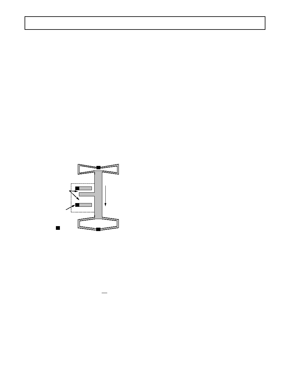
away leaving the suspended sensor element. Figure 14 is a
simplified view of the sensor structure. The actual sensor has
42 unit cells for sensing acceleration. The differential capacitor
sensor is composed of fixed plates and moving plates attached to
the beam that moves in response to acceleration. Movement of
the beam changes the differential capacitance, which is measured
by the on chip circuitry.
The sensor has 12-unit capacitance cells for electrostatically
forcing the beam during a self-test. Self-test is activated by the
user with a logic high on the self-test input pin. During a logic
high, an electrostatic force acts on the beam equivalent to
approximately 20% of full-scale acceleration input, and thus a
proportional voltage change appears on the output pin. When
activated, the self-test feature exercises both the entire mechani-
cal structure and the electrical circuitry.
BEAM
FIXED
PLATE
UNIT CELL
ACCELERATION
ANCHOR
PLATE
CAPACITANCES
Figure 14. Simplified View of Sensor Under Acceleration
All the circuitry needed to drive the sensor and convert the
capacitance change to voltage is incorporated on the chip requiring
no external components except for standard power supply decou-
pling. Both sensitivity and the zero-g value are ratiometric to
the supply voltage, so that ratiometeric devices following the
accelerometer (such as an ADC, etc.) will track the accelerom-
eter if the supply voltage changes. The output voltage (V
OUT
) is
a function of both the acceleration input (a) and the power
supply voltage (V
S
) as follows:
V
OUT
= V
S
/2 (Sensitivity
×
V
S
5V
×
a)
Both the ADXL150 and ADXL250 have a 2-pole Bessel switched-
capacitor filter. Bessel filters, sometimes called linear phase
filters, have a step response with minimal overshoot and a maxi-
mally flat group delay. The 3 dB frequency of the poles is
preset at the factory to 1 kHz. These filters are also completely
self-contained and buffered, requiring no external components.
MEASURING ACCELERATIONS LESS THAN 50 g
The ADXL150/ADXL250 require only a power supply bypass
capacitor to measure
±
50 g accelerations. For measuring
±
50 g
accelerations, the accelerometer may be directly connected to an
ADC (see Figure 25). The device may also be easily modified to
measure lower g signals by increasing its output scale factor.
The scale factor of an accelerometer specifies the voltage change
of the output per g of applied acceleration. This should not be
confused with its resolution. The resolution of the device is the
lowest g level the accelerometer is capable of measuring. Resolu-
tion is principally determined by the device noise and the mea-
surement bandwidth.
The zero g bias level is simply the dc output level of the accelerom-
eter when it is not in motion or being acted upon by the earth's
gravity.
Pin Programmable Scale Factor Option
In its normal state, the ADXL150/ADXL250's buffer amplifier
provides an output scale factor of 38 mV/g, which is set by an
internal voltage divider. This gives a full-scale range of
±
50 g
and a nominal bandwidth of 1 kHz.
A factor-of-two increase in sensitivity can be obtained by con-
necting the V
OUT
pin to the offset null pin, assuming that it is
not needed for offset adjustment. This connection has the effect
of reducing the internal feedback by a factor of two, doubling
the buffer's gain. This increases the output scale factor to 76 mV/g
and provides a
±
25 g full-scale range.
Simultaneously, connecting these two pins also increases the
amount of internal post filtering, reducing the noise floor and
changing the nominal 3 dB bandwidth of the ADXL150/
ADXL250 to 500 Hz. Note that the post filter's "Q" will also
be reduced by a factor of
2 from 0.58 (Bessel response) to a
much gentler "Q" value of 0.41. The primary effect of this
change in "Q" is only at frequencies within two octaves of the
corner frequency; above this the two filter slopes are essentially
the same. In applications where a flat response up to 500 Hz is
needed, it is better to operate the device at 38 mV/g and use an
external post filter. Note also that connecting V
OUT
to the offset
pin adds a 30 k
load from V
OUT
to V
S
/2. When swinging
±
2 V
at V
OUT
, this added load will consume
±
60
µ
A of the ADXL150/
ADXL250's 100
µ
A (typical) output current drive.
8
ADXL150/ADXL250
REV. 0
+V
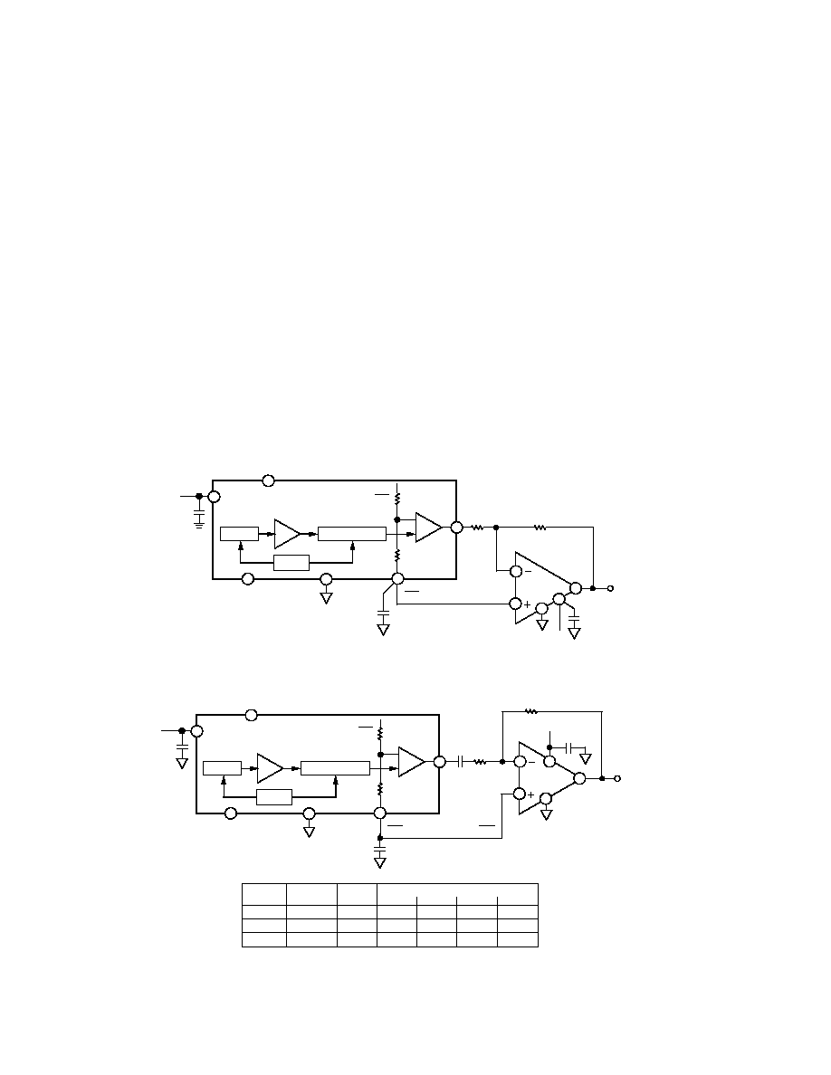
S
2
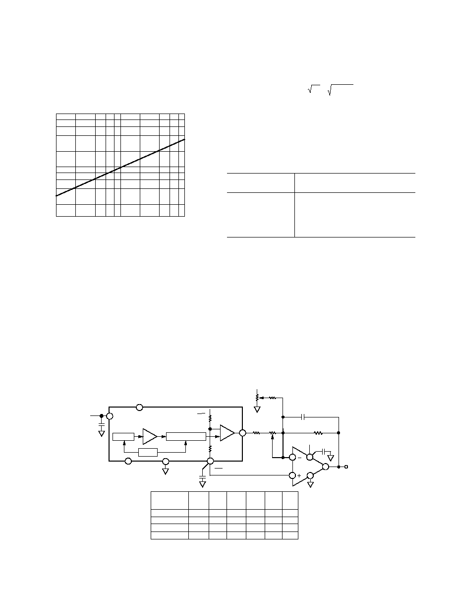
OUTPUT SCALE FACTOR = 38mV/
g
R1
R3
SELF-TEST
+V
S
2
25k
5k
ADXL150
GAIN
AMP
OFFSET
NULL
COM
C1
0.1 F
BUFFER
AMP
DEMODULATOR
SENSOR
+V
S
TP
(DO NOT CONNECT)
14
9
10
7
5
CLOCK
C4
0.1 F
+V
S
OP196
8
3
4
7
6
R1
R3
V
OUT
2
C2
0.1 F
Figure 15. Using an External Op Amp to Increase Output Scale Factor
+V
S
C4
0.1 F
R2
OUTPUT
EXTERNAL AMP GAIN =
R2
1M
+V
S
2
V
OUT
1M
BUFFER
GAIN
FS RANGE
R2
1Hz
3Hz
10Hz
20Hz
2
25
g
1M
0.15 F 0.05 F 0.015 F 0.0075 F
4
12.5
g
332k
0.47 F 0.15 F 0.047 F 0.022 F
5
10
g
249k
0.68 F
0.22 F 0.022 F 0.01 F
C3 VALUE FOR 3dB CORNER FREQ
TYPICAL COMPONENT VALUES FOR AC COUPLED CIRCUIT
C2
0.1 F
+V
S
2
SELF-TEST
+V
S
2
25k
5k
ADXL150
GAIN
AMP
OFFSET
NULL
COM
C1
0.1 F
BUFFER
AMP
DEMODULATOR
SENSOR
+V
S
TP
(DO NOT CONNECT)
14
9
10
7
5
CLOCK
OP196
8
3
4
7
6
2
C3
Figure 16. AC Coupled Connection Using an External Op Amp
Increasing the
i
MEM
S
Accelerometer's Output
Scale Factor
Figure 15 shows the basic connections for using an external
buffer amplifier to increase the output scale factor.
The output multiplied by the gain of the buffer, which is simply
the value of resistor R3 divided by R1. Choose a convenient
scale factor, keeping in mind that the buffer gain not only ampli-
fies the signal, but any noise or drift as well. Too much gain can
also cause the buffer to saturate and clip the output waveform.
Note that the "+" input of the external op amp uses the offset
null pin of the ADXL150/ADXL250 as a reference, biasing the
op amp at midsupply, saving two resistors and reducing power
consumption. The offset null pin connects to the V
S
/2 reference
point inside the accelerometer via 30 k
, so it is important not
to load this pin with more than a few microamps.
It is important to use a single-supply or "rail-to-rail" op amp for
the external buffer as it needs to be able to swing close to the
supply and ground.
The circuit of Figure 15 is entirely adequate for many applica-
tions, but its accuracy is dependent on the pretrimmed accuracy
of the accelerometer and this will vary by product type and grade.
For the highest possible accuracy, an external trim is recom-
mended. As shown by Figure 20, this consists of a potentiom-
eter, R1a, in series with a fixed resistor, R1b. Another option is
to select resistor values after measuring the device's scale factor
(see Figure 17).
AC Coupling
If a dc (gravity) response is not required--for example in vibra-
tion measurement applications--ac coupling can be used be-
tween the accelerometer's output and the external op amp's
input as shown in Figure 16. The use of ac coupling virtually
eliminates any zero g drift and allows the maximum external
amp gain without clipping.
Resistor R2 and capacitor C3 together form a high pass filter
whose corner frequency is 1/(2
R2 C3). This filter will reduce
the signal from the accelerometer by 3 dB at the corner fre-
quency, and it will continue to reduce it at a rate of 6 dB/octave
(20 dB per decade) for signals below the corner frequency.
Capacitor C3 should be a nonpolarized, low leakage type.
If ac coupling is used, the self-test feature must be monitored at
the accelerometer's output rather than at the external amplifier
output (since the self-test output is a dc voltage).
ADXL150/ADXL250
9
REV. 0
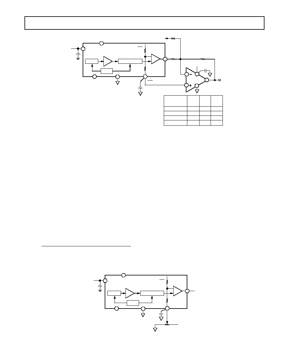
R3
100k
R2 (SEE NOTES)
+V
S
OR GND
+V
S
R1
V
OUT
+V
S
2
SELF-TEST
+V
S
2
25k
5k
ADXL150
GAIN
AMP
OFFSET
NULL
COM
BUFFER
AMP
DEMODULATOR
SENSOR
+V
S
TP
(DO NOT CONNECT)
14
9
10
7
5
CLOCK
OP196
3
4
6
2
8
7
NOTES:
0
g "QUICK" CALIBRATION METHOD USING RESISTOR R2 AND A +5V SUPPLY.
(a) WITH ACCELEROMETER ORIENTED AWAY FROM EARTH'S
GRAVITY (i.e., SIDEWAYS), MEASURE PIN 10 OF THE ADXL150.
(b) CALCULATE THE OFFSET VOLTAGE THAT NEEDS TO BE NULLED:
V
OS
=(+2.5V V
PIN
10)(R3/R1).
2.5V (R3)
V
OS
(
c) R2 =
(d) FOR V
PIN
10 > +2.5V, R2 CONNECTS TO GND.
(e) FOR V
PIN
10 < +2.5V, R2 CONNECTS TO +V
S
.
EXT
AMP
GAIN
R1
VALUE
FS
RANGE
DESIRED
OUTPUT
SCALE FACTOR
76mV/
g
25
g
2.0
49.9k
100mV/
g
20
g
2.6
38.3k
200mV/
g
10
g
5.3
18.7k
400mV/
g
5
g
10.5
9.53k
C2
0.1 F
C1
0.1 F
C4
0.1 F
Figure 17. "Quick Zero g Calibration" Connection
Adjusting the Zero g Bias Level
When a true dc (gravity) response is needed, the output from
the accelerometer
must be dc coupled to the external amplifier's
input. For high gain applications, a zero g offset trim will also be
needed. The external offset trim permits the user to set the zero g
offset voltage to exactly +2.5 volts (allowing the maximum output
swing from the external amplifier without clipping with a +5
supply).
With a dc coupled connection, any difference between the zero g
output and +2.5 V will be amplified along with the signal. To
obtain the exact zero g output desired or to allow the maximum
output voltage swing from the external amplifier, the zero g offset
will need to be externally trimmed using the circuit of Figure 20.
The external amplifier's maximum output swing should be
limited to
±
2 volts, which provides a safety margin of
±
0.25
volts before clipping. With a +2.5 volt zero g level, the maxi-
mum gain will equal:
2 Volts
38 mV/g Times the Max Applied Acceleration in g
The device scale factor and zero g offset levels can be calibrated
using the earth's gravity, as explained in the section "calibrating
the ADXL150/ADXL250."
Using the Zero g "Quick-Cal" Method
In Figure 18 (accelerometer alone, no external op amp), a trim
potentiometer connects directly to the accelerometer's zero g
null pin. The "quick offset calibration" scheme shown in Figure
17 is preferred over using a potentiometer, which could change
its setting over time due to vibration. The "quick offset calibra-
tion" method requires measuring only the output voltage of
the ADXL150/ADXL250 while it is oriented normal to the
earth's gravity. Then, by using the simple equations shown in
the figures, the correct resistance value for R2 can be calculated.
In Figure 17, an external op amp is used to amplify the signal. A
resistor, R2, is connected to the op amp's summing junction.
The other side of R2 connects to either ground or +V
S
depend-
ing on which direction the offset needs to be shifted.
OFFSET
NULL
+V
S
200k
R
IN
AT PIN 8
30k 10k
SELF-TEST
+V
S
2
25k
5k
ADXL150
GAIN
AMP
COM
BUFFER
AMP
DEMODULATOR
SENSOR
+V
S
TP
(DO NOT CONNECT)
V
OUT
14
8
9
10
7
5
CLOCK
C1
0.1 F
C2
0.1 F
Figure 18. Offset Nulling the ADXL150/ADXL250 Using a Trim Potentiometer
10
ADXL150/ADXL250
REV. 0
DEVICE BANDWIDTH VS. MEASUREMENT
RESOLUTION
Although an accelerometer is usually specified according to its
full-scale g level, the limiting resolution of the device, i.e., its
minimum discernible input level, is extremely important when
measuring low g accelerations.
3dB BANDWIDTH Hz
100m
g
1m
g
10m
g
10
1k
100
NOISE LEVEL rms
660m
g
66m
g
6.6m
g
NOISE LEVEL Peak to Peak
Figure 19. ADXL150/ADXL250 Noise Level vs. 3 dB
Bandwidth (Using a "Brickwall" Filter)
The limiting resolution is predominantly set by the measure-
ment noise "floor," which includes the ambient background
noise and the noise of the ADXL150/ADXL250 itself. The level
of the noise floor varies directly with the bandwidth of the mea-
surement. As the measurement bandwidth is reduced, the noise
floor drops, improving the signal-to-noise ratio of the measure-
ment and increasing its resolution.
The bandwidth of the accelerometer can be easily reduced by
adding low-pass or bandpass filtering. Figure 19 shows the
typical noise vs. bandwidth characteristic of the ADXL150/
ADXL250.
The output noise of the ADXL150/ADXL250 scales with the
square root of the measurement bandwidth. With a single pole
roll-off, the equivalent rms noise bandwidth is
divided by 2 or
approximately 1.6 times the 3 dB bandwidth. For example, the
typical rms noise of the ADXL150 using a 100 Hz one pole post
filter is:
Noise rms
( )
=
1mg/ Hz
×
100 1.6
( )
=
12.25 mg
Because the ADXL150/ADXL250's noise is, for all practical
purposes, Gaussian in amplitude distribution, the highest noise
amplitudes have the smallest (yet nonzero) probability. Peak-
to-peak noise is therefore difficult to measure and can only be
estimated due to its statistical nature. Table I is useful for esti-
mating the probabilities of exceeding various peak values, given
the rms value.
Table I.
Nominal Peak-to-
% of Time that Noise Will Exceed
Peak Value
Nominal Peak-to-Peak Value
2.0
×
rms
32%
4.0
×
rms
4.6%
6.0
×
rms
0.27%
6.6
×
rms
0.1%
8.0
×
rms
0.006%
RMS and peak-to-peak noise (for 0.1% uncertainty) for various
bandwidths are estimated in Figure 19. As shown by the figure,
device noise drops dramatically as the operating bandwidth is
reduced. For example, when operated in a 1 kHz bandwidth,
the ADXL150/ADXL250 typically have an rms noise level of
32 mg. When the device bandwidth is rolled off to 100 Hz, the
noise level is reduced to approximately 10 mg.
Alternatively, the signal-to-noise ratio may be improved consid-
erably by using a microprocessor to perform multiple measure-
ments and then to compute the average signal level.
Low-Pass Filtering
The bandwidth of the accelerometer can easily be reduced by using
post filtering. Figure 20 shows how the buffer amplifier can be
connected to provide 1-pole post filtering, zero g offset trimming,
and output scaling. The table provides practical component values
Cf
R2
1M
+V
S
RT
200k
0
g TRIM
SCALE
FACTOR
TRIM
(OPTIONAL)
R3
100k
+V
S
0.1 F
R1a
75k
V
OUT
0.1 F
+V
S
2
SELF-TEST
25k
5k
ADXL150
GAIN
AMP
OFFSET
NULL
COM
C1
0.1 F
BUFFER
AMP
DEMODULATOR
SENSOR
+V
S
TP
(DO NOT CONNECT)
14
9
10
7
5
CLOCK
OP196
3
4
6
2
8
7
+V
S
2
R1b
50k
EXT
AMP
GAIN
R3
VALUE
F.S.
RANGE
DESIRED
OUTPUT
SCALE FACTOR
Cf ( F)
100Hz
Cf ( F)
30Hz
Cf ( F)
10Hz
0.0082
0.0056
0.0033
0.0015
0.027
0.022
0.010
0.0056
0.082
0.056
0.033
0.015
76mV/
g
25
g
2.0
200k
100mV/
g
20
g
2.6
261k
200mV/
g
10
g
5.3
536k
400mV/
g
5
g
10.5
1M
Figure 20. One-Pole Post Filter Circuit with SF and Zero g Offset Trims
ADXL150/ADXL250
11
REV. 0
2-POLE
FILTER
R2
42.2k
R3
82.5k
R1
82.5k
+V
S
200k
0
g TRIM
R6
1M
R5
R4
100k
OUTPUT
SCALING
AMPLIFIER
BW
C3
C4
TYPICAL FILTER VALUES
300Hz
0.027 F 0.0033 F
100Hz
0.082 F 0.01 F
30Hz
0.27 F
0.033 F
10Hz
0.82 F
0.1 F
+V
S
0.1 F
C2
0.1 F
+V
S
2
SELF-TEST
+V
S
2
25k
5k
ADXL150
GAIN
AMP
OFFSET
NULL
COM
C1
0.1 F
BUFFER
AMP
DEMODULATOR
SENSOR
+V
S
TP
(DO NOT CONNECT)
14
9
10
7
5
CLOCK
1/2
OP296
3
1
2
8
8
EXT
AMP
GAIN
R5
VALUE
F.S.
RANGE
DESIRED
OUTPUT
SCALE FACTOR
76mV/
g
±25
g
2.0
200k
100mV/
g
±20
g
2.6
261k
200mV/
g
±10
g
5.3
536k
400mV/
g
±5
g
10.5
1M
C3
C4
+V
S
2
1/2
OP296
5
4
7
6
Figure 21. Two-Pole Post Filter Circuit
for various full-scale g levels and approximate circuit band-
widths. For bandwidths other than those listed, use the
formula:
Cf
=
1
2
R3
(
)
Desired 3dB Bandwidth in Hz
or simply scale the value of capacitor Cf accordingly; i.e., for an
application with a 50 Hz bandwidth, the value of Cf will need
to be twice as large as its 100 Hz value. If further noise reduc-
tion is needed while maintaining the maximum possible band-
width, a 2- or 3-pole post filter is recommended. These provide
a much steeper roll-off of noise above the pole frequency. Fig-
ure 21 shows a circuit that provides 2-pole post filtering. Com-
ponent values for the 2-pole filter were selected to operate the
first op amp at unity gain. Capacitors C3 and C4 were chosen
to provide 3 dB bandwidths of 10 Hz, 30 Hz, 100 Hz and
300 Hz.
The second op amp offsets and scales the output to provide a
+2.5 V
±
2 V output over a wide range of full-scale g levels.
APPLICATION HINTS
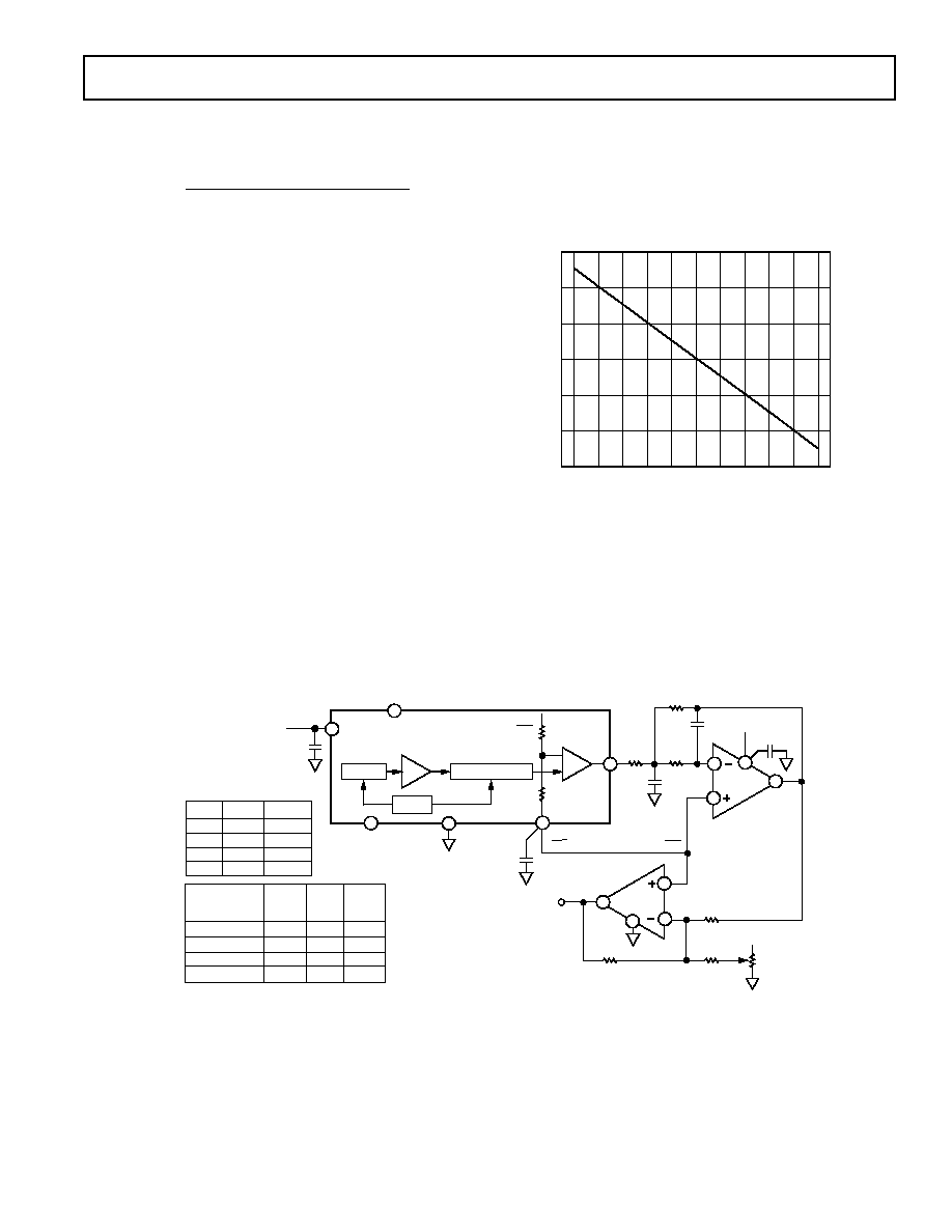
ADXL250 Power Supply Pins
When wiring the ADXL250, be sure to connect BOTH power
supply terminals, Pins 14 and 13.
Ratiometric Operation
Ratiometric operation means that the circuit uses the power
supply as its voltage reference. If the supply voltage varies, the
accelerometer and the other circuit components (such as an
ADC, etc.) track each other and compensate for the change.
Figure 22 shows how both the zero g offset and output sensitiv-
ity of the ADXL150/ADXL250 vary with changes in supply
voltage. If they are to be used with nonratiometric devices, such
as an ADC with a built-in 5 V reference, then both components
should be referenced to the same source, in this case the ADC
reference. Alternatively, the circuit can be powered from an
external +5 volt reference.
POWER SUPPLY VOLTAGE
2.65
2.50
2.35
5.25 5.20 5.15 5.10 5.05 5.00 4.95 4.90
4.85 4.80 4.75
2.60
2.55
2.45
2.40
40.25
38.00
35.75
SENSITIVITY
39.50
38.75
37.25
36.50
0
g
OFFSET
Figure 22. Typical Ratiometric Operation
Since any voltage variation is transferred to the accelerometer's
output, it is important to reduce any power supply noise. Simply
following good engineering practice of bypassing the power supply
right at Pin 14 of the ADXL150/ADXL250 with a 0.1
µ
F ca-
pacitor should be sufficient.
12
ADXL150/ADXL250
REV. 0
Additional Noise Reduction Techniques
Shielded wire should be used for connecting the accelerometer to
any circuitry that is more than a few inches away--to avoid 60 Hz
pickup from ac line voltage. Ground the cable's shield at only one
end and connect a separate common lead between the circuits;
this will help to prevent ground loops. Also, if the accelerometer
is inside a metal enclosure, this should be grounded as well.
Mounting Fixture Resonances
A common source of error in acceleration sensing is resonance
of the mounting fixture. For example, the circuit board that the
ADXL150/ADXL250 mounts to may have resonant frequencies
in the same range as the signals of interest. This could cause the
signals measured to be larger than they really are. A common
solution to this problem is to damp these resonances by mount-
ing the ADXL150/ADXL250 near a mounting post or by add-
ing extra screws to hold the board more securely in place.
When testing the accelerometer in your end application, it is
recommended that you test the application at a variety of fre-
quencies to ensure that no major resonance problems exist.
REDUCING POWER CONSUMPTION
The use of a simple power cycling circuit provides a dramatic
reduction in the accelerometer's average current consumption.
In low bandwidth applications such as shipping recorders, a
simple, low cost circuit can provide substantial power reduction.
If a microprocessor is available, it can supply a TTL clock pulse
to toggle the accelerometer's power on and off.
A 10% duty cycle, 1 ms on, 9 ms off, reduces the average cur-
rent consumption of the accelerometer from 1.8 mA to 180
µ
A,
providing a power reduction of 90%.
Figure 23 shows the typical power-on settling time of the
ADXL150/ADXL250.
TIME ms
4.5
4.0
3.5
3.0
2.5
2.0
1.5
1.0
0.5
0
5.0
0
0.04
VOLTAGE Volts
0.08
0.12
0.16
0.20
0.24
0.28
0.32
0.36
V
S
0.5V
V
OUT
50
g
V
OUT
= 0
g
V
OUT
+ 50
g
0.5V
Figure 23. Typical Power-On Settling with Full-Scale
Input. Time Constant of Post Filter Dominates the
Response When a Signal Is Present.
CALIBRATING THE ADXL150/ADXL250
If a calibrated shaker is not available, both the zero g level and
scale factor of the ADXL150/ADXL250 may be easily set to fair
accuracy by using a self-calibration technique based on the 1 g
acceleration of the earth's gravity. Figure 24 shows how gravity
and package orientation affect the ADXL150/ADXL250's
output. With its axis of sensitivity in the vertical plane, the
ADXL150/ADXL250 should register a 1 g acceleration, either
positive or negative, depending on orientation. With the axis of
sensitivity in the horizontal plane, no acceleration (the zero g
bias level) should be indicated. The use of an external buffer
amplifier may invert the polarity of the signal.
0
g
(a)
0
g
(b)
+1
g
(c)
1
g
(d)
8
14
1
7
8
14
7
1
8
7
1
14
1
14
7
8
Figure 24. Using the Earth's Gravity to Self-
Calibrate the ADXL150/ADXL250
Figure 24 shows how to self-calibrate the ADXL150/ADXL250.
Place the accelerometer on its side with its axis of sensitivity
oriented as shown in "a." (For the ADXL250 this would be the
"X" axis--its "Y" axis is calibrated in the same manner, but the
part is rotated 90
°
clockwise.) The zero g offset potentiometer
RT is then roughly adjusted for midscale: +2.5 V at the external
amp output (see Figure 20).
Next, the package axis should be oriented as in "c" (pointing
down) and the output reading noted. The package axis should
then be rotated 180
°
to position "d" and the scale factor poten-
tiometer, R1b, adjusted so that the output voltage indicates a
change of 2 gs in acceleration. For example, if the circuit scale
factor at the external buffer's output is 100 mV per g, the scale
factor trim should be adjusted so that an output change of
200 mV is indicated.
Self-Test Function
A Logic "1" applied to the self-test (ST) input will cause an
electrostatic force to be applied to the sensor that will cause it to
deflect. If the accelerometer is experiencing an acceleration
when the self-test is initiated, the output will equal the algebraic
sum of the two inputs. The output will stay at the self-test level
as long as the ST input remains high, and will return to the
actual acceleration level when the ST voltage is removed.
Using an external amplifier to increase output scale factor may
cause the self-test output to overdrive the buffer into saturation.
The self-test may still be used in this case, but the change in the
output must then be monitored at the accelerometer's output
instead of the external amplifier's output.
Note that the value of the self-test delta is not an exact indica-
tion of the sensitivity (mV/g) and therefore may not be used to
calibrate the device for sensitivity error.
ADXL150/ADXL250
13
REV. 0
MINIMIZING EMI/RFI
The architecture of the ADXL150/ADXL250, and its use of
synchronous demodulation, makes the device immune to most
electromagnetic (EMI) and radio frequency (RFI) interference.
The use of synchronous demodulation allows the circuit to
reject all signals except those at the frequency of the oscillator
driving the sensor element. However, the ADXL150/ADXL250
have a sensitivity to noise on the supply lines that is near its
internal clock frequency (approximately 100 kHz) or its odd
harmonics and can exhibit baseband errors at the output. These
error signals are the beat frequency signals between the clock
and the supply noise.
Such noise can be generated by digital switching elsewhere in
the system and must be attenuated by proper bypassing. By
inserting a small value resistor between the accelerometer and
its power supply, an RC filter is created. This consists of the
resistor and the accelerometer's normal 0.1
µ
F bypass capacitor.
For example if R = 20
and C = 0.1
µ
F, a filter with a pole at
80 kHz is created, which is adequate to attenuate noise on the
supply from most digital circuits, with proper ground and sup-
ply layout.
Power supply decoupling, short component leads, physically
small (surface mount, etc.) components and attention to good
grounding practices all help to prevent RFI and EMI problems.
Good grounding practices include having separate analog and
digital grounds (as well as separate power supplies or very good
decoupling) on the printed circuit boards.
INTERFACING THE ADXL150/ADXL250 SERIES
i
MEM
S
ACCELEROMETERS WITH POPULAR ANALOG-TO-
DIGITAL CONVERTERS.
Basic Issues
The ADXL150/ADXL250 Series accelerometers were designed
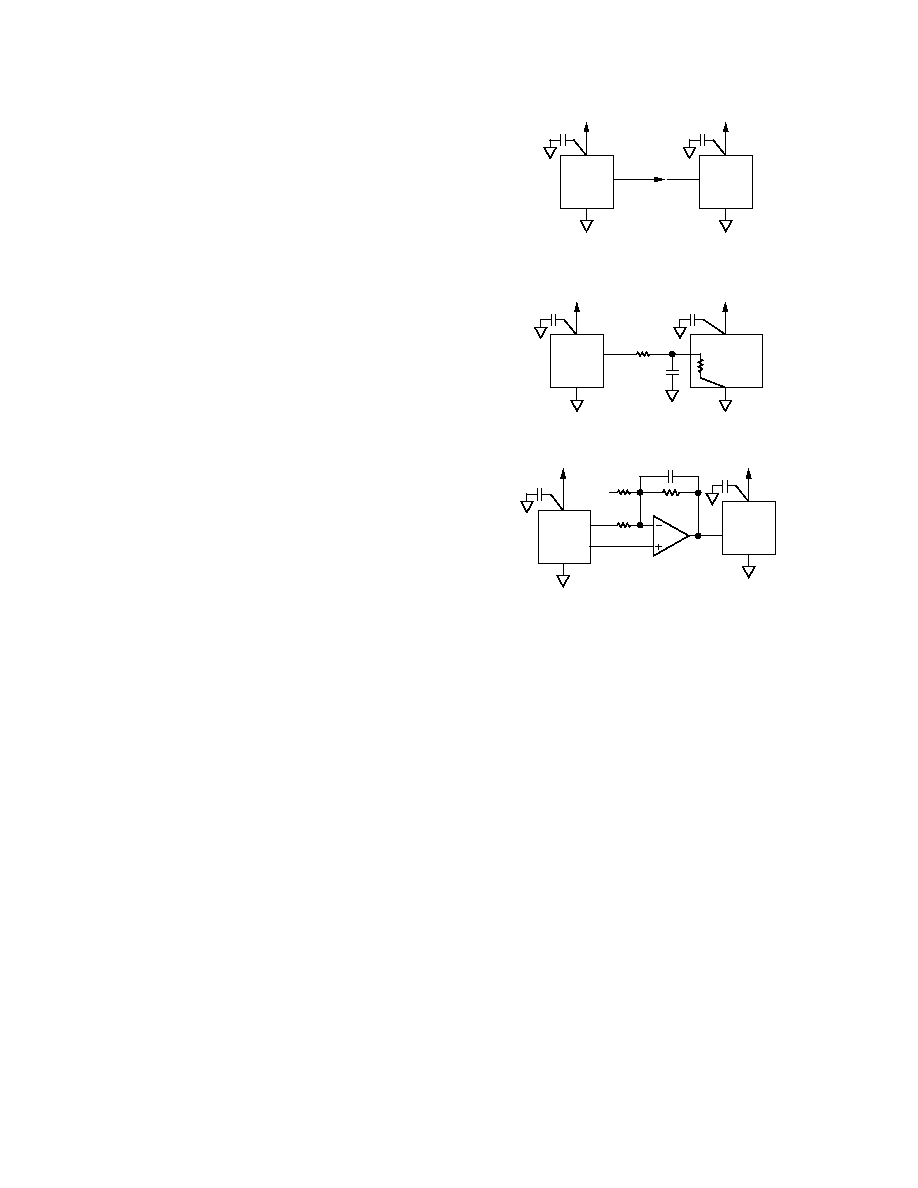
to drive popular analog-to-digital converters (ADCs) directly.
In applications where both a
±
50 g full-scale measurement range
and a 1 kHz bandwidth are needed, the V
OUT
terminal of the
accelerometer is simply connected to the V
IN
terminal of the
ADC as shown in Figure 25a. The accelerometer provides its
(nominal) factory preset scale factor of +2.5 V
±
38 mV/g which
drives the ADC input with +2.5 V
±
1.9 V when measuring a
50 g full-scale signal (38 mV/g
×
50 g = 1.9 V).
As stated earlier, the use of post filtering will dramatically
improve the accelerometer's low g resolution. Figure 25b shows
a simple post filter connected between the accelerometer and
the ADC. This connection, although easy to implement, will
require fairly large values of Cf, and the accelerometer's signal
will be loaded down (causing a scale factor error) unless the
ADC's input impedance is much greater than the value of Rf.
ADC input impedance's range from less than 1.5 k
up to
greater than 15 k
with 5 k
values being typical. Figure 25c is
the preferred connection for implementing low-pass filtering
with the added advantage of providing an increase in scale
factor, if desired.
Calculating ADC Requirements
The resolution of commercial ADCs is specified in bits. In an
ADC, the available resolution equals 2
n
, where n is the number
of bits. For example, an 8-bit converter provides a resolution of
2
8
which equals 256. So the full-scale input range of the converter
divided by 256 will equal the smallest signal it can resolve.
In selecting an appropriate ADC to use with our accelerometer
we need to find a device that has a resolution better than the
measurement resolution but, for economy's sake, not a great
deal better.
For most applications, an 8- or 10-bit converter is appropriate.
The decision to use a 10-bit converter alone, or to use a gain
stage together with an 8-bit converter, depends on which is more
important: component cost or parts count and ease of assembly.
Table II shows some of the tradeoffs involved.
Table II.
8-Bit Converter and 10-Bit (or 12-Bit)
Op Amp Preamp
Converter
Advantages:
Low Cost Converter
No Zero g Trim Required
Disadvantages:
Needs Op Amp
Higher Cost Converter
Needs Zero g Trim
Adding amplification between the accelerometer and the ADC
will reduce the circuit's full-scale input range but will greatly
reduce the resolution requirements (and therefore the cost) of
the ADC. For example, using an op amp with a gain of 5.3
following the accelerometer will increase the input drive to the
ADC from 38 mV/g to 200 mV/g. Since the signal has been
gained up, but the maximum full-scale (clipping) level is still the
same, the dynamic range of the measurement has also been
reduced by 5.3.
Table III. Typical System Resolution Using Some Popular
ADCs Being Driven with and without an Op Amp Preamp
Converter
SF
FS
System
Converter
mV/Bit
Preamp in
Range
Resolution
Type
2
n
(5 V/2
n
)
Gain
mV/g
in g's
in g's (p-p)
8 Bit
256
19.5 mV
None
38
±
50
0.51
256
19.5 mV
2
76
±
25
0.26
256
19.5 mV
2.63
100
±
20
0.20
256
19.5 mV
5.26
200
±
10
0.10
10 Bit
1,024 4.9 mV
None
38
±
50
0.13
1,024 4.9 mV
2
76
±
25
0.06
1,024 4.9 mV
2.63
100
±
20
0.05
1,024 4.9 mV
5.26
200
±
10
0.02
12 Bit
4,096 1.2 mV
None
38
±
50
0.03
4,096 1.2 mV
2
76
±
25
0.02
4,096 1.2 mV
2.63
100
±
20
0.01
4,096 1.2 mV
5.26
200
±
10
0.006
Table III is a chart showing the required ADC resolution vs. the
scale factor of the accelerometer with or without a gain ampli-
fier. Note that the system resolution specified in the table refers
14
ADXL150/ADXL250
REV. 0
to that provided by the converter and preamp (if used). It is
necessary to use sufficient post filtering with the accelerometer
to reduce its noise floor to allow full use of the converter's reso-
lution (see post filtering section).
The use of a gain stage following the accelerometer will nor-
mally require the user to adjust the zero g offset level (either by
trimming or by resistor selection--see previous sections).
For many applications, a modern "economy priced" 10-bit
converter, such as the AD7810 allows you to have high resolu-
tion without using a preamp or adding much to the overall
circuit cost. In addition to simplicity and cost, it also meets two
other necessary requirements: it operates from a single +5 V
supply and is very low power.
+V
S
V
OUT
XL
+V
S
ADC
a. Direct Connection, No Signal Amplification or
Post Filtering
R
F
+V
S
V
OUT
XL
+V
S
ADC
INPUT
RESISTANCE
Cf
b. Single-Pole Post Filtering, No Signal Amplification
V
OS
NULL PIN
0
g
OFFSET
ADJUST
+V
S
V
OUT
XL
+V
S
ADC
R
F
Cf
R1
c. Single-Pole Post Filtering and Signal Amplification
Figure 25. Interfacing the ADXL150/ADXL250 Series
Accelerometers to an ADC
ADXL150/ADXL250
15
REV. 0
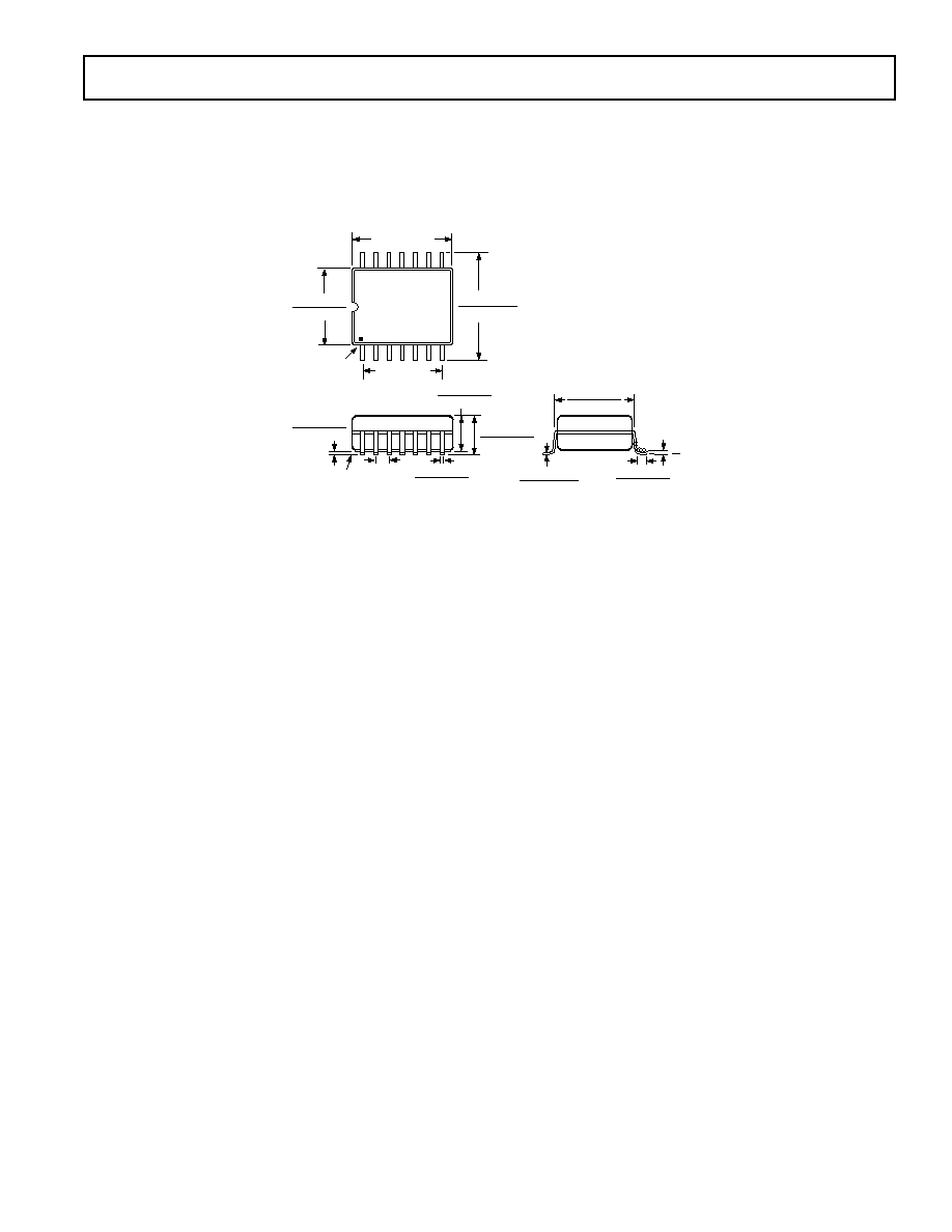
OUTLINE DIMENSIONS
Dimensions shown in inches and (mm).
14-Lead Cerpac
(QC-14)
0.291 (7.391)
0.285 (7.239)
0.390 (9.906)
MAX
PIN 1
0.419 (10.643)
0.394 (10.008)
7
14
8
1
0.300 (7.62)
0.345 (8.763)
0.290 (7.366)
0.0125 (0.318)
0.009 (0.229)
0.050 (1.270)
0.016 (0.406)
8
0
SEATING
PLANE
0.020 (0.508)
0.004 (0.102)
0.020 (0.508)
0.013 (0.330)
0.050
(1.27)
BSC
0.195 (4.953)
0.115 (2.921)
0.215 (5.461)
0.119 (3.023)
C294984/98
PRINTED IN U.S.A.