 | ÐлекÑÑоннÑй компоненÑ: ADVFC32 | СкаÑаÑÑ:  PDF PDF  ZIP ZIP |
Äîêóìåíòàöèÿ è îïèñàíèÿ www.docs.chipfind.ru

REV. A
Information furnished by Analog Devices is believed to be accurate and
reliable. However, no responsibility is assumed by Analog Devices for its
use, nor for any infringements of patents or other rights of third parties
which may result from its use. No license is granted by implication or
otherwise under any patent or patent rights of Analog Devices.
a
Voltage-to-Frequency and
Frequency-to-Voltage Converter
ADVFC32
One Technology Way, P.O. Box 9106, Norwood, MA 02062-9106, U.S.A.
Tel: 617/329-4700
Fax: 617/326-8703
FEATURES
High Linearity
0.01% max at 10 kHz FS
0.05% max at 100 kHz FS
0.2% max at 500 kHz FS
Output TTL/CMOS Compatible
V/F or F/V Conversion
6 Decade Dynamic Range
Voltage or Current Input
Reliable Monolithic Construction
MIL-STD-883 Compliant Versions Available
PRODUCT DESCRIPTION
The industry standard ADVFC32 is a low cost monolithic
voltage-to-frequency (V/F) converter or frequency-to-voltage
(F/V) converter with good linearity (0.01% max error at
10 kHz) and operating frequency up to 0.5 MHz. In the V/F
configuration, positive or negative input voltages or currents can
be converted to a proportional frequency using only a few exter-
nal components. For F/V conversion, the same components are
used with a simple biasing network to accommodate a wide
range of input logic levels.
TTL or CMOS compatibility is achieved in the V/F operating
mode using an open collector frequency output. The pullup re-
sistor can be connected to voltages up to 30 volts, or to +15 V
or +5 V for conventional CMOS or TTL logic levels. This resis-
tor should be chosen to limit current through the open collector
output to 8 mA. A larger resistance can be used if driving a high
impedance load.
Input offset drift is only 3ppm of full scale per
°
C, and full-
scale calibration drift is held to a maximum of 100 ppm/
°
C
(ADVFC32BH) due to a low T.C. Zener diode.
The ADVFC32 is available in commercial, industrial, and ex-
tended temperature grades. The commercial grade is packaged
in a 14-pin plastic DIP while the two wider temperature range
parts are packaged in hermetically sealed TO-100 cans.
PRODUCT HIGHLIGHTS
1. The ADVFC32 uses a charge balancing circuit technique
(see Functional Block Diagram) which is well suited to high
accuracy voltage-to-frequency conversion. The full-scale
operating frequency is determined by only one precision re-
sistor and capacitor. The tolerance of other support compo-
nents (including the integration capacitor) is not critical.
Inexpensive
±
20% resistors and capacitors can be used with-
out affecting linearity or temperature drift.
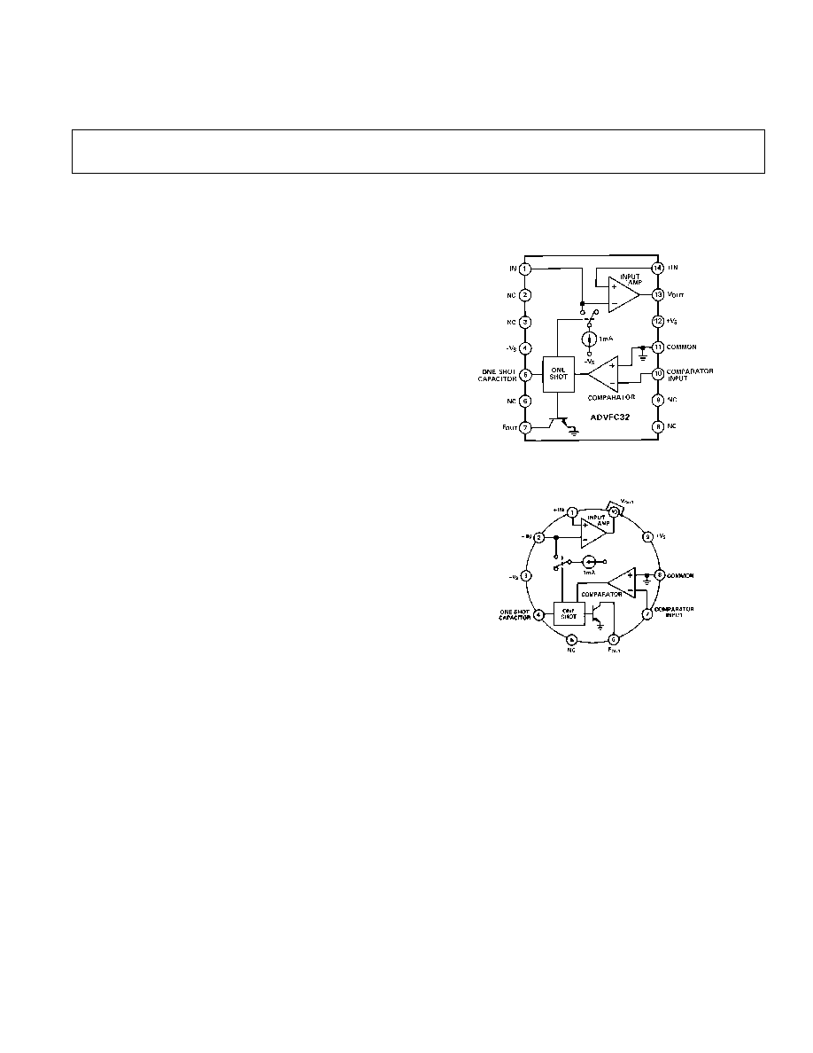
PIN CONFIGURATION
(TOP VIEW)
"N" Package
"H" Package TO-100
NC = NO CONNECT
2. The ADVFC32 is easily configured to satisfy a wide range of
system requirements. Input voltage scaling is set by selecting
the input resistor which sets the input current to 0.25 mA at
the maximum input voltage.
3. The same components used for V/F conversion can also be
used for F/V conversion by adding a simple logic biasing net-
work and reconfiguring the ADVFC32.
4. The ADVFC32 is intended as a pin-for-pin replacement for
VFC32 devices from other manufacturers.
5. The ADVFC32 is available in versions compliant with MIL-
STD-883. Refer to the Analog Devices Military Products
Databook or current ADVFC32/883B data sheet for detailed
specifications.

REV. A
2
ADVFC32SPECIFICATIONS
(typical @ +25 C with V
S
= 15 V unless otherwise noted)
Specifications shown in boldface are tested on all production units at
final electrical test. Results from those tests are used to calculate
outgoing quality levels. All min and max specifications are guaranteed,
although only those shown in boldface are tested on all production units.
ADVFC32K
ADVFC32B
ADVFC32S
Model
Min
Typ
Max
Min
Typ
Max
Min
Typ
Max
Units
DYNAMIC PERFORMANCE
Full Scale Frequency Range
0
500
0
500
0
500
kHz
Nonlinearity
1
f
MAX
= 10 kHz
0.01
±
0.01
0.01
+0.01
0.01
+0.01
%
f
MAX
= 100 kHz
0.05
+0.05
0.05
+0.05
0.05
+0.05
%
f
MAX
= 0.5 MHz
0.20
±
0.05
+0.20
0.20
±
0.05
+0.20
0.20
±
0.05
+0.20
%
Full-Scale Calibration Error
(Adjustable to Zero)
±
5
±
5
±
5
%
vs. Supply
(Full Scale Frequency = 100 kHz)
0.015
+0.015
0.015
+0.015
0.015
+0.015
% of FSR%
vs. Temperature
(Full Scale Frequency = 10 kHz)
±
75
100
+100
+150
+150
ppm/
°
C
DYNAMIC RESPONSE
Maximum Settling Time for Full Scale
Step Input
1 Pulse of New Frequency Plus 1
µ
s
1 Pulse of New Frequency Plus 1
µ
s
1 Pulse of New Frequency Plus 1
µ
s
Overload Recovery Time
1 Pulse of New Frequency Plus 1
µ
s
1 Pulse of New Frequency Plus 1
µ
s
1 Pulse of New Frequency Plus 1
µ
s
ANALOG INPUT AMPLIFIER
(V/F Conversion)
Current Input Range
0
+0.25
0
+0.25
0
+0.25
mA
Voltage Input Range
0
10
0
10
0
10
V
2
0.25
0.25
0.25
mA
×
R
IN
3
×
R
IN
3
×
R
IN
3
Differential Impedance
300 k
||
10 pF
2 M
||
10 pF
300 k
||
10 pF
2 M
||
10 pF
300 k
||
10 pF
2 M
||
10 pF
Common-Mode Impedance
300 M
||
3 pF
750 M
||
3 pF
300 M
||
3 pF
750 M
||
10 pF
300 M
||
3 pF
750 M
||
10 pF
Input Bias Current
Noninverting Input
40
250
40
250
40
250
nA
Inverting Input
100
±
8
+100
100
±
8
+100
100
±
8
+100
nA
Input Offset Voltage
(Trimmable to Zero)
2, 3
4
4
4
mV
vs. Temperature (T
MIN
to T
MAX
)
30
30
30
µ
V/
°
C
Safe Input Voltage
±
V
S
±
V
S
±
V
S
COMPARATOR (F/V Conversion)
Logic "0" Level
V
S
0.6
V
S
0.6
V
S
0.6
V
Logic "1" Level
+1
+V
S
+1
+V
S
+1
+V
S
V
Pulse Width Range
4
0.1
0.15/f
MAX
0.1
0.15/f
MAX
0.1
0.15/f
MAX
µ
s
Input Impedance
50 k
||
10 pF
250 k
50 k
||
10 pF
250 k
50 k
||
10 pF
250 k
OPEN COLLECTOR OUTPUT
(V/F Conversion)
Output Voltage in Logic "0"
I
SINK
= 8 mA
0.4
0.4
0.4
V
Output Leakage Current in Logic "1"
1
1
1
µ
A
Voltage Range
0
+30
0
+30
0
+30
V
Fall Times (Load = 500 pF and
I
SINK
= 5 mA)
400
400
400
ns
AMPLIFIER OUTPUT (F/V Conversion)
Voltage Range (0 mA
I
O
7 mA)
0
+10
0
+10
0
+10
V
Source Current (0
V
O
7 V)
10
10
10
mA
Capacitive Load (Without Oscillation)
100
100
100
pF
Closed Loop Output Impedance
1
1
1
POWER SUPPLY
Rated Voltage
±
15
±
15
±
15
V
Voltage Range
±
9
±
18
±
9
±
18
±
9
±
18
V
Quiescent Current
6
8
6
8
6
8
mA
TEMPERATURE RANGE
Specified Range
0
+70
25
+85
55
+125
°
C
Operating Range
25
+85
55
+125
55
+125
°
C
Storage
25
+85
65
+150
65
+150
°
C
PACKAGE OPTIONS
Plastic DIP (N-14)
ADVFC32KN
TO100 (H-10A)
ADVFC32BH
ADVFC32SH
NOTES
1
Nonlinearity defined as deviation from a straight line from zero to full scale, expressed as a percentage of full scale.
2
See Figure 3.
3
See Figure 1.
4
f
MAX
expressed in units of MHz.
Specifications subject to change without notice.

ADVFC32
REV. A
3
UNIPOLAR V/F, POSITIVE INPUT VOLTAGE
When operated as a V/F converter, the transformation from
voltage to frequency is based on a comparison of input signal
magnitude to the 1 mA internal current source.
A more complete understanding of the ADVFC32 requires a
close examination of the internal circuitry of this part. Consider
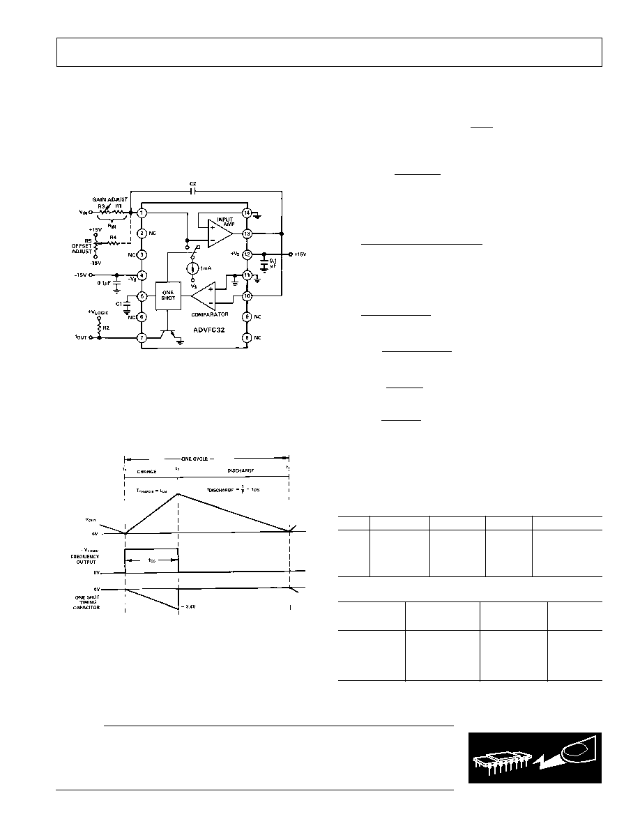
the operation of the ADVFC32 when connected as shown in
Figure 1. At the start of a cycle, a current proportional to the
Figure 1. Connection Diagram for V/F Conversion,
Positive Input Voltage
input voltage flows through R3 and R1 to charge integration
capacitor C2. As charge builds up on C2, the output voltage of
the input amplifier decreases. When the amplifier output volt-
age (Pin 13) crosses ground (see Figure 2 at time t
1
), the
comparator triggers a one shot whose time period is determined
Figure 2. Voltage-to-Frequency Conversion Waveforms
by capacitor C1. Specifically, the one shot time period (in nano-
seconds) is:
t
OS
(C
l
+ 44 pF)
×
6.7 k
During this period, a current of (1 mA I
IN
) flows out of the in-
tegration capacitor. The total amount of charge depleted during
one cycle is, therefore (1 mA I
IN
)
×
t
OS
. This charge is replaced
during the remainder of the cycle to return the integrator to its
original voltage. Since the charge taken out of C2 is equal to the
charge that is put on C2 every cycle,
(1 mA I
IN
)
×
t
OS
= I
IN
×
1
F
OUT
t
OS
or, rearranging terms,
F
OUT
=
I
IN
1 mA
×
t
OS
The complete transfer equation can now be derived by substi-
tuting I
IN
= V
IN
/R
IN
and the equation relating C1 and t
OS
. The
final equation describing ADVFC32 operation is:
V
IIN
/ R
IN
1mA
×
C
1
+
44 pF
(
)
×
6.7 k
Components should be selected to optimize performance over
the desired input voltage and output frequency range using the
equations listed below:
3.7
×
10
7
pF / sec
F
OUT FS
44 pF
C
2
=
10
4
Farads / sec
F
OUT FS
1000 pF minimum
(
)
R
IN
=
V
IN FS
0.25 mA
R
2
+
V
LOGIC
8 mA
Both R
IN
and C
1
should have very low temperature coefficients
as changes in their values will result in a proportionate change in
the V/F transfer function. Other component values and tem-
perature coefficients are not critical.
WARNING!
ESD SENSITIVE DEVICE
CAUTION
ESD (electrostatic discharge) sensitive device. Electrostatic charges as high as 4000 V readily
accumulate on the human body and test equipment and can discharge without detection.
Although the ADVFC32 features proprietary ESD protection circuitry, permanent damage may
occur on devices subjected to high energy electrostatic discharges. Therefore, proper ESD
precautions are recommended to avoid performance degradation or loss of functionality.
ORDERING GUIDE
Part
Gain Tempco
Temp Range
Package
Number
1
ppm/ C
C
Option
ADVFC32KN
±
75 typ
0 to +70
14-Pin
Plastic DIP
ADVFC32BH
±
100 max
25 to +85
TO-100
ADVFC32SH
±
150 max
55 to +125
TO-100
NOTE
1
For details on grade and package offerings screened in accordance with
MIL-STD-883, refer to the Analog Devices Military Products Databook or current
ADVFC32/883B data sheet.
Table I. Suggested Values for C
1
, R
IN
and C
2
V
IN FS
F
OUT FS
C
1
R
IN
C
2
1 V
10 kHz
3650 pF
4.0 k
0.01
µ
F
10 V
10 kHz
3650 pF
40 k
0.01
µ
F
1 V
100 kHz
330 pF
4.0 k
1000 pF
10 V
100 kHz
330 pF
40 k
1000 pF

ADVFC32
4
REV. A
F/V CONVERSION
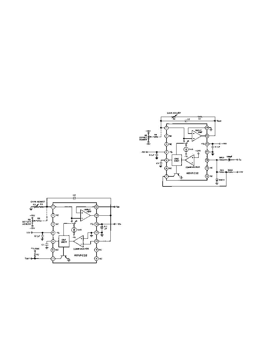
Although the mathematics of F/V conversion can be very com-
plex, the basic principle is easy to understand. Figure 4 shows
the connection diagram for F/V conversion with TTL input
logic levels. Each time the input signal crosses the comparator
threshold going negative, the one shot is activated and switches
1 mA into the integrator input for a measured time period (de-
termined by C1). As the frequency increases, the amount of
charge injected into the integration capacitor increases propor-
tionately. The voltage across the integration capacitor is stabi-
lized when the leakage current through R1 and R3 equals the
average current being switched into the integrator. The net re-
sult of these two effects is an average output voltage which is
proportional to the input frequency. Optimum performance can
be obtained by selecting components using the same guidelines
and equations listed in the V/F conversion section.
Figure 4. Connection Diagram for F/V Conversion, TTL
Input
DECOUPLING
Decoupling power supplies at the device is good practice in any
system, but absolutely imperative in high resolution applica-
tions. For the ADVFC32, it is important to remember where
the voltage transients and ground currents flow. For example,
the current drawn through the output pulldown transistor origi-
nates from the logic supply, and is directed to ground through
Pin 11 (Pin 8 of TO-100). Therefore, the logic supply should be
decoupled near the ADVFC32 to provide a low impedance re-
turn path for switching transients. Also, if there is a separate
digital ground it should be connected to the analog ground at
the ADVFC32. This will prevent ground offsets that could be
created by directing the full 8 mA output current into the analog
ground, and subsequently back to the logic supply.
Although some circuits may operate satisfactorily with the
power supplies decoupled at only one location on each board,
this practice is not recommended for the ADVFC32. For best
results, each supply should be decoupled with 0.1
µ
F capacitor
at the ADVFC32. In addition, a larger board level decoupling
capacitor of 1
µ
F to 10
µ
F should be located relatively close to
the ADVFC32 on each power supply.
COMPONENT TEMPERATURE COEFFICIENTS
The drift specifications of the ADVFC32 do not include tem-
perature effects of any of the supporting resistors or capacitors.
The drift of the input resistors R1 and R3 and the timing ca-
pacitor C1 directly affect the overall temperature stability. In the
application of Figure 2, a 10 ppm/
°
C input resistor used with a
Input resistance R
IN
is composed of a fixed resistor (R1) and a
variable resistor (R3) to allow for initial gain error compensation.
To cover all possible situations, R3 should be 20% of R
IN
, and
R1 should be 90% of R
IN
. This allows a
±
10% gain adjustment
to compensate for the ADVFC32 full-scale error and the toler-
ance of C1.
If more accurate initial offset is required, the circuit of R4 and
R5 can be added. R5 can have a value between 10 k
and
100 k
, and R4 should be approximately 10 M
. The amount
of current required to trim zero offset will be relatively small, so
the temperature coefficients of these resistors are not critical. If
large offsets are added using this circuit, temperature drift of
both of these resistors is much more important.
BIPOLAR V/F
By adding another resistor from Pin 1 (Pin 2 of TO-100 can) to
a stable positive voltage, the ADVFC32 can be operated with a
bipolar input voltage. For example, an 80 k
resistor to +10 V
causes an additional current of 0.125 mA to flow into the inte-
grator so that the net current flow to the integrator is positive
even for negative input voltages. At negative full-scale input
voltage, 0.125 mA will flow into the integrator from V
IN
cancel-
ling out the 0.125 mA from the offset resistor, resulting in an
output frequency of zero. At positive full scale, the sum of the
two currents will be 0.25 mA and the output will be at its maxi-
mum frequency.
UNIPOLAR V/F, NEGATIVE INPUT VOLTAGE
Figure 3 shows the connection diagram for V/F conversion of
negative input voltages. In this configuration full-scale output
frequency occurs at negative full-scale input, and zero output
frequency corresponds to zero input voltage.
Figure 3. Connection Diagram for V/F Conversion,
Negative Input Voltage
A very high impedance signal source may be used since it only
drive the noninverting integrator input. Typical input imped-
ance at this terminal is 250 M
or higher. For V/F conversion
of positive input signals the signal generator must be able to
source 0.25 mA to properly drive the ADVFC32, but for nega-
tive V/F conversion the 0.25 mA integration current is drawn
from ground through R1 and R3.
Circuit operation for negative input voltages is very similar to
positive input unipolar conversion described in the previous sec-
tion. For best operating results use component equations listed
in that section.

ADVFC32
REV. A
5
100 ppm/
°
C capacitor may result in a maximum overall circuit
gain drift of:
100 ppm/
°
C (ADVFC32BH) + 100 ppm/
°
C (C1)
+ 10 ppm/
°
C (R
IN
) = 210 ppm/
°
C
Although R
IN
and C1 have the most pronounced effect on tem-
perature stability, the offset circuit of resistors R4 and R5 may
also have a slight effect on the offset temperature drift of the cir-
cuit. The offset will change with variations in the resistance of
R4 and supply voltage changes. In most applications the offset
adjustment is very small, and the offset drift attributable to this
circuit will be negligible. In the bipolar mode, however, both the
positive reference and the resistor used to offset the signal range
will have a pronounced effect on offset drift. A high quality
reference and resistor should be used to minimize offset drift
errors.
Other circuit components do not directly influence temperature
performance as long as their actual values are not so different
from nominal value as to preclude operation. This includes
integration capacitor C2. A change in the capacitance value of
C2 results in a different rate of voltage change across C2, but
this is compensated by an equal effect when C2 is discharged by
the switched 1 mA current source so that no net effect occurs.
The temperature effects of the components described above are
the same when the ADVFC32 is configured for negative or bi-
polar input ranges, or F/V conversion.
OTHER CIRCUIT CONSIDERATIONS
The input amplifier connected to Pins 1, 13, and 14 is not a
standard operational amplifier. Although it operates like an op
amp in most applications, two key differences should be noted.
First, the bias current of the positive input is typically 40 nA
while the bias current of the inverting input is
±
8 nA. Therefore,
any attempt to cancel input offset voltage due to bias currents by
matching input resistors will create worse offsets. Second, the
output of this amplifier will sink only 1 mA, even though it will
source as much as 10 mA. When used in the F/V mode, the am-
plifier must be buffered if large sink currents are required.
MICROPROCESSOR OPERATED A/D CONVERTER
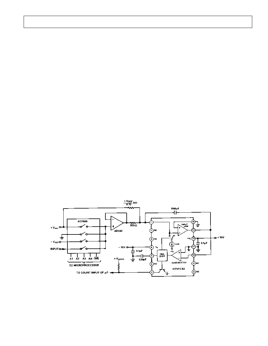
With the addition of a few external components the ADVFC32
can be used as a
±
10 V A/D microprocessor front end. Although
the nonlinearity of the ADVFC32 is only 0.05% maximum
(0.01% typ), the resolution is much higher, allowing it to be
used in 16-bit measurement and control systems where a mono-
tonic transfer function is essential. The resolution of the circuit
shown in Figure 5 is dependent on the amount of time allowed
to count the ADVFC32 frequency output. Using a full scale fre-
quency of 100 kHz, an 8-bit conversion can be made in about
10 ms, and a 2 second time period allows a 16-bit measurement,
including offset and gain calibration cycles.
As shown in Figure 5, the input signal is selected via the AD7590
input multiplexer. Positive and negative references as well as a
ground input are provided to calibrate the A/D. This is very im-
portant in systems subject to moderate or extreme temperature
changes since the gain temperature coefficient of the ADVFC32
is as high as
±
150 ppm/
°
C. By using the calibration cycles, the
A/D conversion will be as accurate as the references provided.
The AD542 following the input multiplexer provides a high im-
pedance input (10
12
ohms) and buffers the switch resistance
from the relatively low impedance ADVFC32 input.
If higher linearity is required, the ADVFC32 can be operated at
10 kHz, but this will require a proportionately longer conver-
sion, time. Conversely, the conversion time can be decreased at
the expense of nonlinearity by increasing the maximum fre-
quency to as high as 500 kHz.
HIGH NOISE IMMUNITY, HIGH CMRR ANALOG DATA
LINK
In many applications, a signal must be sensed at a remote site
and sent through a very noisy environment to a central location
for further processing. In these cases, even a shielded cable may
not protect the signal from noise pickup. The circuit of Figure 6
provides a solution in these cases. Due to the optocoupler and
Figure 5. High Resolution, Self-Calibrating, Microprocessor
Operated A/D Converter
voltage-to-frequency conversion, this data link is extremely
insensitive to noise and common-mode voltage interference. For
even more protection, an optical fiber link substituted for the
HCPL2630 will provide common-mode rejection of more than
several hundred kilovolts and virtually total immunity to electri-
cal noise. For most applications, however, the frequency modu-
lated signal has sufficient noise immunity without using an optical
