 | ÐлекÑÑоннÑй компоненÑ: ADV7196A | СкаÑаÑÑ:  PDF PDF  ZIP ZIP |
Äîêóìåíòàöèÿ è îïèñàíèÿ www.docs.chipfind.ru
REV. 0
Information furnished by Analog Devices is believed to be accurate and
reliable. However, no responsibility is assumed by Analog Devices for its
use, nor for any infringements of patents or other rights of third parties that
may result from its use. No license is granted by implication or otherwise
under any patent or patent rights of Analog Devices.
a
ADV7196A
One Technology Way, P.O. Box 9106, Norwood, MA 02062-9106, U.S.A.
Tel: 781/329-4700
www.analog.com
Fax: 781/326-8703
© Analog Devices, Inc., 2001
Multiformat Progressive Scan/HDTV
Encoder with Three 11-Bit DACs,
10-Bit Data Input, and Macrovision
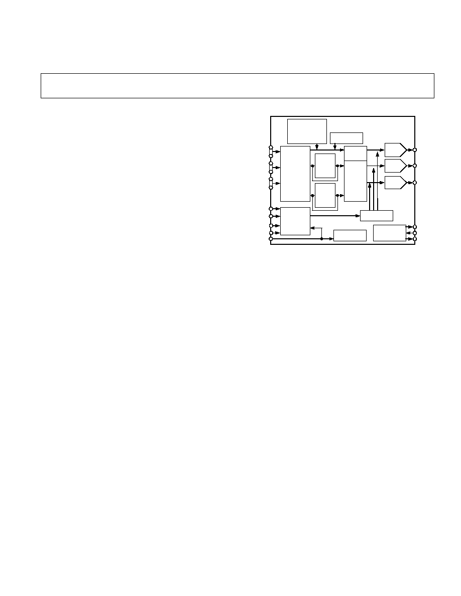
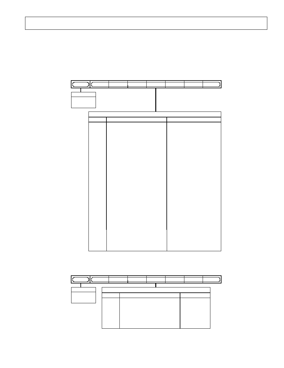
FUNCTIONAL BLOCK DIAGRAM
CGMS
MACROVISION
SHARPNESS
FILTER CONTROL
AND
ADAPTIVE
FILTER CONTROL
TEST PATTERN
GENERATOR
AND
DELAY
AND
GAMMA
CORRECTION
Y0Y9
Cr0Cr9
Cb0Cb9
CHROMA
4:2:2
TO
4:4:4
(SSAF)
2
INTER-
POLATION
TIMING
GENERATOR
SYNC
GENERATOR
I
2
C MPU
PORT
CLKIN
HORIZONTAL
SYNC
VERTICAL
SYNC
BLANKING
RESET
ADV7196A
DAC CONTROL
BLOCK
DAC A (Y)
DAC B
DAC C
V
REF
RESET
COMP
11-BIT+
SYNC
DAC
11-BIT
DAC
11-BIT
DAC
LUMA
SSAF
CHROMA
4:2:2
TO
4:4:4
(SSAF)
FEATURES
INPUT FORMATS
YCrCb in 2
10-Bit (4:2:2) or 3 10-Bit (4:4:4) Format
Compliant to SMPTE-293M (525p), ITU-R.BT1358
(625p), SMPTE274M (1080i), SMPTE296M (720p) and
Any Other High Definition Standard Using Async
Timing Mode
RGB in 3
10 Bit (4:4:4) Format
OUTPUT FORMATS
YPrPb Progressive Scan (EIA-770.1, EIA-770.2)
YPrPb HDTV (EIA-770.3)
RGB Levels Compliant to RS-170 and RS-343A
11-Bit and Sync (DAC A)
11-Bit DACs (DAC B, DAC C)
PROGRAMMABLE FEATURES
Internal Test Pattern Generator with Color Control
Y/C Delay ( )
Gamma Correction
Individual DAC On/Off Control
54 MHz Output (2 Oversampling)
Sharpness Filter with Programmable Gain/Attenuation
Programmable Adaptive Filter Control
Undershoot Limiter
I
2
C
®
Filter
VBI Open Control
Macrovision Rev. 1.0 (525p)
CGMS-A (525p)
2-Wire Serial MPU Interface
Single Supply 3.3 V Operation
52-MQFP Package
APPLICATIONS
Progressive Scan/HDTV Display Devices
DVD Players
MPEG 2 at 81 MHz
Progressive Scan/HDTV Projection Systems
Digital Video Systems
High Resolution Color Graphics
Image Processing/Instrumentation
Digital Radio Modulation/Video Signal Reconstruction
I
2
C is a registered trademark of Philips Corporation.
GENERAL DESCRIPTION
The ADV7196A is a triple high-speed, digital-to-analog encoder
on a single monolithic chip. It consists of three high-speed video
D/A converters with TTL-compatible inputs.
The ADV7196A has three separate 10-bit-wide input ports which
accept data in 4:4:4 10-bit YCrCb or RGB or 4:2:2 10-bit YCrCb.
This data is accepted in progressive scan format at 27 MHz or
HDTV format at 74.25 MHz or 74.1758 MHz. For any other
high-definition standard but SMPTE 293M, ITU-R BT.1358,
SMPTE274M or SMPTE296M the Async Timing Mode can be
used to input data to the ADV7196A. For all standards, external
horizontal, vertical, and blanking signals or EAV/SAV codes control
the insertion of appropriate synchronization signals into the digital
data stream and therefore the output signals.
The ADV7196A outputs analog YPrPb progressive scan format
complying to EIA-770.1, EIA-770.2; YPrPb HDTV complying
to EIA-770.3; RGB complying to RS-170/RS-343A.
The ADV7196A requires a single 3.3 V power supply, an
optional external 1.235 V reference and a 27 MHz clock in
Progressive Scan Mode or a 74.25 MHz (or 74.1758 MHz)
clock in HDTV mode.
In Progressive Scan Mode, a sharpness filter with programmable
gain allows high-frequency enhancement on the luminance signal.
Programmable Adaptive Filter Control, which may be used, allows
removal of ringing on the incoming Y data. The ADV7196A
supports CGMS-A data control generation and the Macrovision
Anticopy algorithm in 525p mode.
The ADV7196A is packaged in a 52-lead MQFP package.

REV. 0
ADV7196A
2
TABLE OF CONTENTS
FEATURES . . . . . . . . . . . . . . . . . . . . . . . . . . . . . . . . . . . . . 1
GENERAL DESCRIPTION . . . . . . . . . . . . . . . . . . . . . . . . . 1
FUNCTIONAL BLOCK DIAGRAM . . . . . . . . . . . . . . . . . 1
3.3 V SPECIFICATIONS . . . . . . . . . . . . . . . . . . . . . . . . . . . 4
3 V DYNAMICSPECIFICATIONS . . . . . . . . . . . . . . . . . . 4
3.3 V TIMINGSPECIFICATIONS . . . . . . . . . . . . . . . . . . 5
ABSOLUTE MAXIMUM RATINGS . . . . . . . . . . . . . . . . . 8
ORDERING GUIDE . . . . . . . . . . . . . . . . . . . . . . . . . . . . . . 8
PIN CONFIGURATION . . . . . . . . . . . . . . . . . . . . . . . . . . . 8
PIN FUNCTION DESCRIPTIONS . . . . . . . . . . . . . . . . . . 9
FUNCTIONAL DESCRIPTION . . . . . . . . . . . . . . . . . . . . 10
Digital Inputs . . . . . . . . . . . . . . . . . . . . . . . . . . . . . . . . . . 10
Control Signals . . . . . . . . . . . . . . . . . . . . . . . . . . . . . . . . 10
Analog Outputs . . . . . . . . . . . . . . . . . . . . . . . . . . . . . . . . 10
I
2
C Filters . . . . . . . . . . . . . . . . . . . . . . . . . . . . . . . . . . . . 10
Undershoot Limiter . . . . . . . . . . . . . . . . . . . . . . . . . . . . . 10
Internal Test Pattern Generator . . . . . . . . . . . . . . . . . . . . 10
Y/CrCb Delay . . . . . . . . . . . . . . . . . . . . . . . . . . . . . . . . . 10
Gamma Correction . . . . . . . . . . . . . . . . . . . . . . . . . . . . . 10
54 MHz Operation . . . . . . . . . . . . . . . . . . . . . . . . . . . . . . 10
PROGRAMMABLE SHARPNESS FILTER . . . . . . . . . . . 10
PROGRAMMABLE ADAPTIVE FILTER CONTROL . . 10
Input/Output Configuration . . . . . . . . . . . . . . . . . . . . . . . 11
MPU PORT DESCRIPTION . . . . . . . . . . . . . . . . . . . . . . . 11
REGISTER ACCESSES . . . . . . . . . . . . . . . . . . . . . . . . . . . 12
REGISTER PROGRAMMING . . . . . . . . . . . . . . . . . . . . . 13
Subaddress Register (SR7SR0) . . . . . . . . . . . . . . . . . . . 13
Register Select (SR6SR0) . . . . . . . . . . . . . . . . . . . . . . . . 13
PROGRESSIVE SCAN MODE . . . . . . . . . . . . . . . . . . . . . 14
MODE REGISTER 0 . . . . . . . . . . . . . . . . . . . . . . . . . . . 14
MR0 (MR07MR00) . . . . . . . . . . . . . . . . . . . . . . . . . . . . 14
MR0 BIT DESCRIPTION . . . . . . . . . . . . . . . . . . . . . . . . . 14
Output Standard Selection (MR00MR01) . . . . . . . . . . . 14
Input Control Signals (MR02MR03) . . . . . . . . . . . . . . . 14
Input Standard (MR04) . . . . . . . . . . . . . . . . . . . . . . . . . . 14
Reserved (MR05) . . . . . . . . . . . . . . . . . . . . . . . . . . . . . . . 14
DV Polarity (MR06) . . . . . . . . . . . . . . . . . . . . . . . . . . . . 14
Macrovision (MR07) . . . . . . . . . . . . . . . . . . . . . . . . . . . . 14
MODE REGISTER 1 . . . . . . . . . . . . . . . . . . . . . . . . . . . . . 16
MR1 (MR17MR10) . . . . . . . . . . . . . . . . . . . . . . . . . . . . 16
MR1 BIT DESCRIPTION . . . . . . . . . . . . . . . . . . . . . . . . . 16
Pixel Data Enable (MR10) . . . . . . . . . . . . . . . . . . . . . . . . 16
Input Format (MR11) . . . . . . . . . . . . . . . . . . . . . . . . . . . 16
Test Pattern Enable (MR12) . . . . . . . . . . . . . . . . . . . . . . 16
Test Pattern Hatch/Frame (MR13) . . . . . . . . . . . . . . . . . 16
VBI Open (MR14) . . . . . . . . . . . . . . . . . . . . . . . . . . . . . . 16
Undershoot Limiter (MR15MR16) . . . . . . . . . . . . . . . . 16
Sharpness Filter (MR17) . . . . . . . . . . . . . . . . . . . . . . . . . 16
MODE REGISTER 2 . . . . . . . . . . . . . . . . . . . . . . . . . . . . . 17
MR1 (MR27MR20) . . . . . . . . . . . . . . . . . . . . . . . . . . . . 17
MR2 BIT DESCRIPTION . . . . . . . . . . . . . . . . . . . . . . . . . 17
Y Delay (MR20MR22) . . . . . . . . . . . . . . . . . . . . . . . . . 17
Color Delay (MR23MR25) . . . . . . . . . . . . . . . . . . . . . . 17
CGMS Enable (MR26) . . . . . . . . . . . . . . . . . . . . . . . . . . 17
CGMS CRC (MR27) . . . . . . . . . . . . . . . . . . . . . . . . . . . 17
MODE REGISTER 3 . . . . . . . . . . . . . . . . . . . . . . . . . . . . . 18
MR3 (MR37MR30) . . . . . . . . . . . . . . . . . . . . . . . . . . . . 18
MR3 BIT DESCRIPTION . . . . . . . . . . . . . . . . . . . . . . . . . 18
HDTV Enable (MR30) . . . . . . . . . . . . . . . . . . . . . . . . . . 18
Reserved (MR31MR32) . . . . . . . . . . . . . . . . . . . . . . . . . 18
DAC A Control (MR33) . . . . . . . . . . . . . . . . . . . . . . . . . 18
DAC B Control (MR34) . . . . . . . . . . . . . . . . . . . . . . . . . 18
DAC C Control (MR35) . . . . . . . . . . . . . . . . . . . . . . . . . 18
Interpolation (MR36) . . . . . . . . . . . . . . . . . . . . . . . . . . . 18
Reserved (MR37) . . . . . . . . . . . . . . . . . . . . . . . . . . . . . . . 18
MODE REGISTER 4 . . . . . . . . . . . . . . . . . . . . . . . . . . . . . 18
MR4 (MR47MR40) . . . . . . . . . . . . . . . . . . . . . . . . . . . . 18
MR4 BIT DESCRIPTION . . . . . . . . . . . . . . . . . . . . . . . . . 18
Timing Reset (MR40) . . . . . . . . . . . . . . . . . . . . . . . . . . . 18
MODE REGISTER 5 . . . . . . . . . . . . . . . . . . . . . . . . . . . . . 18
MR5 (MR57MR50) . . . . . . . . . . . . . . . . . . . . . . . . . . . . 18
MR5 BIT DESCRIPTION . . . . . . . . . . . . . . . . . . . . . . . . . 18
Reserved (MR50) . . . . . . . . . . . . . . . . . . . . . . . . . . . . . . . 18
RGB Mode (MR51) . . . . . . . . . . . . . . . . . . . . . . . . . . . . . 18
Sync on PrPb (MR52) . . . . . . . . . . . . . . . . . . . . . . . . . . . 18
Color Output Swap (MR53) . . . . . . . . . . . . . . . . . . . . . . 18
Gamma Curve (MR54) . . . . . . . . . . . . . . . . . . . . . . . . . . 19
Gamma Correction (MR55) . . . . . . . . . . . . . . . . . . . . . . 19
Adaptive Mode Control (MR56) . . . . . . . . . . . . . . . . . . . 19
Adaptive Filter Control (MR57) . . . . . . . . . . . . . . . . . . . 19
COLOR Y . . . . . . . . . . . . . . . . . . . . . . . . . . . . . . . . . . . . . . 19
CY (CY7CY0) . . . . . . . . . . . . . . . . . . . . . . . . . . . . . . . . 19
COLOR CR . . . . . . . . . . . . . . . . . . . . . . . . . . . . . . . . . . . . 19
CCR (CCR7CCR0) . . . . . . . . . . . . . . . . . . . . . . . . . . . . 19
COLOR CB . . . . . . . . . . . . . . . . . . . . . . . . . . . . . . . . . . . . 19
CCB (CCB7CCB0) . . . . . . . . . . . . . . . . . . . . . . . . . . . . 19
MODE REGISTER 6 . . . . . . . . . . . . . . . . . . . . . . . . . . . . . 20
MR6 (MR67MR60) . . . . . . . . . . . . . . . . . . . . . . . . . . . . 20
MR6 BIT DESCRIPTION . . . . . . . . . . . . . . . . . . . . . . . . . 20
MR67MR60 . . . . . . . . . . . . . . . . . . . . . . . . . . . . . . . . . . 20
CGMS DATA REGISTERS 20 . . . . . . . . . . . . . . . . . . . . 20
CGMS2 (CGMS27CGMS20) . . . . . . . . . . . . . . . . . . . . 20
CGMS1 (CGMS17CGMS10) . . . . . . . . . . . . . . . . . . . . 20
CGMS0 (CGMS07CGMS00) . . . . . . . . . . . . . . . . . . . . 20
FILTER GAIN . . . . . . . . . . . . . . . . . . . . . . . . . . . . . . . . . . 21
FG (FG7FG0) . . . . . . . . . . . . . . . . . . . . . . . . . . . . . . . . 21
FG BIT DESCRIPTION . . . . . . . . . . . . . . . . . . . . . . . . . . 21
Filter Gain A (FG3FG0) . . . . . . . . . . . . . . . . . . . . . . . . 21
Filter Gain B (FG4FG7) . . . . . . . . . . . . . . . . . . . . . . . . 21
GAMMA CORRECTION REGISTERS 013 . . . . . . . . . . 21
(GAMMA CORRECTION 013) . . . . . . . . . . . . . . . . . . 21
SHARPNESS FILTER CONTROL AND
ADAPTIVE FILTER CONTROL . . . . . . . . . . . . . . . . . 22
SHARPNESS FILTER MODE . . . . . . . . . . . . . . . . . . . . . 22
ADAPTIVE FILTER MODE . . . . . . . . . . . . . . . . . . . . . . . 22
ADAPTIVE FILTER GAIN 1 . . . . . . . . . . . . . . . . . . . . . . 23
AFG1 (AFG1)70 . . . . . . . . . . . . . . . . . . . . . . . . . . . . . . 23
ADAPTIVE FILTER GAIN 2 . . . . . . . . . . . . . . . . . . . . . . 23
AFG2 (AFG2)70 . . . . . . . . . . . . . . . . . . . . . . . . . . . . . . 23

REV. 0
ADV7196A
3
ADAPTIVE FILTER GAIN 3 . . . . . . . . . . . . . . . . . . . . . . 23
AFG3 (AFG3)70 . . . . . . . . . . . . . . . . . . . . . . . . . . . . . . 23
ADAPTIVE FILTER THRESHOLD A . . . . . . . . . . . . . . . 23
AFTA (AFTA)70 . . . . . . . . . . . . . . . . . . . . . . . . . . . . . . 23
ADAPTIVE FILTER THRESHOLD B . . . . . . . . . . . . . . . 23
AFTB (AFTB)70 . . . . . . . . . . . . . . . . . . . . . . . . . . . . . . 23
ADAPTIVE FILTER THRESHOLD C . . . . . . . . . . . . . . . 23
AFTC (AFTC)70 . . . . . . . . . . . . . . . . . . . . . . . . . . . . . 23
SHARPNESS FILTER AND ADAPTIVE FILTER
APPLICATION EXAMPLES . . . . . . . . . . . . . . . . . . . . . 24
Sharpness Filter Application . . . . . . . . . . . . . . . . . . . . . . 24
Adaptive Filter Control Application . . . . . . . . . . . . . . . . . 25
HDTV MODE . . . . . . . . . . . . . . . . . . . . . . . . . . . . . . . . . . 26
MODE REGISTER 0 . . . . . . . . . . . . . . . . . . . . . . . . . . . . . 26
MR0 (MR07MR00) . . . . . . . . . . . . . . . . . . . . . . . . . . . . 26
HEXMR0 BIT DESCRIPTION . . . . . . . . . . . . . . . . . . . . . 26
Output Standard Selection (MR00MR01) . . . . . . . . . . . 26
Input Control Signals (MR02MR03) . . . . . . . . . . . . . . . 26
Reserved (MR04) . . . . . . . . . . . . . . . . . . . . . . . . . . . . . . . 26
Input Standard (MR05) . . . . . . . . . . . . . . . . . . . . . . . . . . 26
DV Polarity (MR06) . . . . . . . . . . . . . . . . . . . . . . . . . . . . 26
Reserved (MR07) . . . . . . . . . . . . . . . . . . . . . . . . . . . . . . . 26
MODE REGISTER 1 . . . . . . . . . . . . . . . . . . . . . . . . . . . . . 27
MR1 (MR17MR10) . . . . . . . . . . . . . . . . . . . . . . . . . . . . 27
MR1 BIT DESCRIPTION . . . . . . . . . . . . . . . . . . . . . . . . . 27
Pixel Data Enable (MR10) . . . . . . . . . . . . . . . . . . . . . . . . 27
Input Format (MR11) . . . . . . . . . . . . . . . . . . . . . . . . . . . 27
Test Pattern Enable (MR12) . . . . . . . . . . . . . . . . . . . . . . 27
Test Pattern Hatch/Frame (MR13) . . . . . . . . . . . . . . . . . 27
VBI Open (MR14) . . . . . . . . . . . . . . . . . . . . . . . . . . . . . . 27
Reserved (MR15MR17) . . . . . . . . . . . . . . . . . . . . . . . . . 27
MODE REGISTER 2 . . . . . . . . . . . . . . . . . . . . . . . . . . . . . 28
MR1 (MR27MR20) . . . . . . . . . . . . . . . . . . . . . . . . . . . . 28
MR2 BIT DESCRIPTION . . . . . . . . . . . . . . . . . . . . . . . . . 28
Y Delay (MR20MR22) . . . . . . . . . . . . . . . . . . . . . . . . . 28
Color Delay (MR23MR25) . . . . . . . . . . . . . . . . . . . . . . 28
Reserved (MR26MR27) . . . . . . . . . . . . . . . . . . . . . . . . . 28
MODE REGISTER 3 . . . . . . . . . . . . . . . . . . . . . . . . . . . . . 28
MR3 (MR37MR30) . . . . . . . . . . . . . . . . . . . . . . . . . . . . . 28
MR3 BIT DESCRIPTION . . . . . . . . . . . . . . . . . . . . . . . . . 28
HDTV Enable (MR30) . . . . . . . . . . . . . . . . . . . . . . . . . . 28
Reserved (MR31MR32) . . . . . . . . . . . . . . . . . . . . . . . . . 28
DAC A Control (MR33) . . . . . . . . . . . . . . . . . . . . . . . . . 28
DAC B Control (MR34) . . . . . . . . . . . . . . . . . . . . . . . . . 28
DAC C Control (MR35) . . . . . . . . . . . . . . . . . . . . . . . . . 28
Reserved (MR36MR37) . . . . . . . . . . . . . . . . . . . . . . . . . 28
MODE REGISTER 4 . . . . . . . . . . . . . . . . . . . . . . . . . . . . . 29
MR4 (MR47MR40) . . . . . . . . . . . . . . . . . . . . . . . . . . . . 29
MR4 BIT DESCRIPTION . . . . . . . . . . . . . . . . . . . . . . . . . 29
Timing Reset (MR40) . . . . . . . . . . . . . . . . . . . . . . . . . . . 29
MODE REGISTER 5 . . . . . . . . . . . . . . . . . . . . . . . . . . . . . 29
MR5 (MR57MR50) . . . . . . . . . . . . . . . . . . . . . . . . . . . . 29
MR5 BIT DESCRIPTION . . . . . . . . . . . . . . . . . . . . . . . . . 29
Reserved (MR50) . . . . . . . . . . . . . . . . . . . . . . . . . . . . . . . 29
RGB Mode (MR51) . . . . . . . . . . . . . . . . . . . . . . . . . . . . . 29
Sync on PrPb (MR52) . . . . . . . . . . . . . . . . . . . . . . . . . . . 29
Color Output Swap (MR53) . . . . . . . . . . . . . . . . . . . . . . 29
Reserved (MR54MR57) . . . . . . . . . . . . . . . . . . . . . . . . . 29
DAC TERMINATION AND LAYOUT
CONSIDERATIONS . . . . . . . . . . . . . . . . . . . . . . . . . . . 30
Voltage Reference . . . . . . . . . . . . . . . . . . . . . . . . . . . . . . 30
PC BOARD LAYOUT CONSIDERATIONS . . . . . . . . . . 30
Supply Decoupling . . . . . . . . . . . . . . . . . . . . . . . . . . . . . . 31
Digital Signal Interconnect . . . . . . . . . . . . . . . . . . . . . . . . 31
Analog Signal Interconnect . . . . . . . . . . . . . . . . . . . . . . . 31
Video Output Buffer and Optional Output Filter . . . . . . . 31
OUTLINE DIMENSIONS . . . . . . . . . . . . . . . . . . . . . . . . . 36

REV. 0
4
ADV7196ASPECIFICATIONS
3.3 V SPECIFICATIONS
Parameter
Min
Typ
Max
Unit
Test Conditions
STATIC PERFORMANCE
Resolution (Each DAC)
11
Bits
Integral Nonlinearity
1.5
LSB
Differential Nonlinearity
0.9
2.0
LSB
DIGITAL OUTPUTS
Output High Voltage, V
OL
0.4
V
I
SINK
= 3.2 mA
Output Low Voltage, V
OH
2.4
V
I
SOURCE
= 400
µA
Three State Leakage Current
10
µA
V
IN
= 0.4 V
Three State Output Capacitance
4
pF
DIGITAL AND CONTROL INPUTS
Input High Voltage, V
IH
2
V
Input Low Voltage, V
IL
0.8
0.65
V
Input Current, I
IN
0
1
µA
V
IN
= 0.0 V or V
DD
Input Capacitance, C
IN
4
pF
ANALOG OUTPUTS
Full-Scale Output Current
3.92
4.25
4.56
mA
DAC A
Output Current Range
3.92
4.25
4.56
mA
DAC A
Full-Scale Output Current
2.54
2.83
3.11
mA
DAC B, C
Output Current Range
2.39
2.66
2.93
mA
DAC B, C
DAC-to-DAC Matching
1.4
%
Output Compliance Range, V
OC
0
1.4
V
Output Impedance, R
OUT
100
k
Output Capacitance, C
OUT
7
pF
VOLTAGE REFERENCE (External)
Reference Range, V
REF
1.112
1.235
1.359
V
POWER REQUIREMENTS
I
DD
2
25
35
mA
1
× Interpolation
I
DD
2
51
60
mA
2
× Interpolation
I
DD
2
40
mA
HDTV Mode
(with f
CLK
= 74.25 MHz)
I
AA
3, 4
11
15
mA
1
× Interpolation, 2× Interpola-
tion, and HDTV Mode
I
PLL
6.0
12
mA
1
× Interpolation, 2× Interpola-
tion, and HDTV Mode
Power Supply Rejection Ratio
0.01
%/%
NOTES
1
Guaranteed by characterization.
2
I
DD
or the circuit current is the continuous current required to drive the digital core without I
PLL
.
3
I
AA
is the total current required to supply all DACs including the V
REF
circuitry.
4
All DACs on.
Specifications subject to change without notice.
(V
AA
= 3.15 V to 3.45 V, V
REF
= 1.235 V, R
SET
= 2470
, R
LOAD
= 300
. All specifications T
MIN
to T
MAX
(0 C to 70 C) unless otherwise noted.)
3 V DYNAMICSPECIFICATIONS
Parameter
Min
Typ
Max
Unit
Luma Bandwidth
13.5
MHz
Chroma Bandwidth
6.75
MHz
Signal-to-Noise Ratio
64
dB Luma Ramp Unweighted
Chroma/Luma Delay Inequality
0
ns
Specifications subject to change without notice.
(V
AA
= 3.15 V to 3.45 V, V
REF
= 1.235 V, R
SET
= 2470
, R
LOAD
= 300
. All specifications
T
MIN
to T
MAX
(0 C to 70 C) unless otherwise noted.)
REV. 0
5
ADV7196A
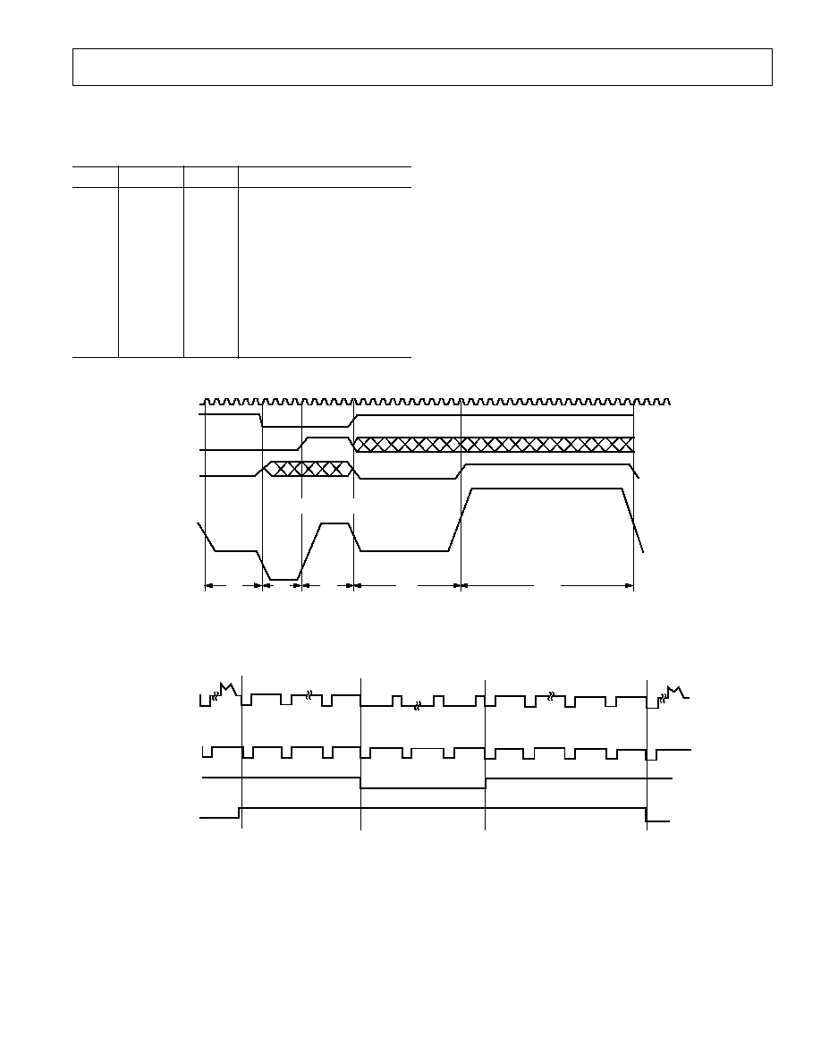
3.3 V TIMINGSPECIFICATIONS
P
arameter
Min
Typ
Max
Unit
Conditions
MPU PORT
1
SCLOCK Frequency
0
400
kHz
SCLOCK High Pulsewidth, t
1
0.6
µs
SCLOCK Low Pulsewidth, t
2
1.3
µs
Hold Time (Start Condition), t
3
0.6
µs
After This Period the 1st Clock Is Generated
Setup Time (Start Condition), t
4
0.6
µs
Relevant for Repeated Start Condition
Data Setup Time, t
5
100
ns
SDATA, SCLOCK Rise Time, t
6
300
ns
SDATA, SCLOCK Fall Time, t
7
300
ns
Setup Time (Stop Condition), t
8
0.6
µs
Reset Low Time
100
ns
ANALOG OUTPUTS
Analog Output Delay
2
10
ns
Analog Output Skew
0.5
ns
CLOCK CONTROL AND PIXEL PORT
3
f
CLK
27
MHz
Progressive Scan Mode
f
CLK
74.25
MHz
HDTV Mode
f
CLK
81
MHz
Async Timing Mode and
1
× Interpolation
Clock High Time t
9
5.0
1.5
ns
Clock Low Time t
10
5.0
2.0
ns
Data Setup Time t
11
2.0
ns
Data Hold Time t
12
4.5
ns
Control Setup Time t
11
7.0
ns
Control Hold Time t
12
4.0
ns
Pipeline Delay
16
Clock Cycles
For 4:4:4 Pixel Input Format at
1
× Oversampling
Pipeline Delay
29
Clock Cycles
For 4:4:4 or 4:2:2 Pixel Input Format at
2
×
Oversampling
NOTES
1
Guaranteed by characterization.
2
Output delay measured from 50% point of the rising edge of CLOCK to the 50% point of DAC output full-scale transition.
3
Data: Cb/Cr [90], Cr [90], Y [9:0]
Control:
HSYNC/SYNC, VSYNC/TSYNC, DV
Specifications subject to change without notice.
(V
AA
= 3.15 V to 3.45 V, V
REF
= 1.235 V, R
SET
= 2470
, R
LOAD
= 300 . All specifications
T
MIN
to T
MAX
(0 C to 70 C) unless otherwise noted.)
REV. 0
ADV7196A
6
B0
B1
B2
B3
Bxxx
Bxxx
CLOCK
PIXEL INPUT
DATA
R0
G0
R1
G1
R2
G2
G3
Rxxx
Gxxx
Rxxx
Gxxx
t
11
t
12
t
9
t
10
t
9
CLOCK HIGH TIME
t
10
CLOCK LOW TIME
t
11
DATA SETUP TIME
t
12
DATA HOLD TIME
· · ·
· · ·
· · ·
· · ·
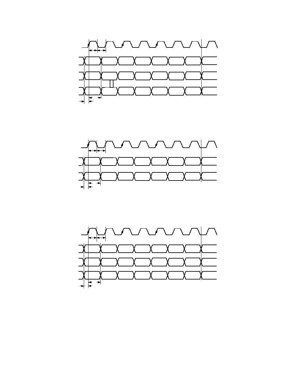
Figure 1. 4:4:4 RGB Input Data Format Timing Diagram
CLOCK
PIXEL INPUT
DATA
Y0
Cb0
Y1
Cr0
Y2
Cb1
Cr1
Yxxx
Cbxxx
Yxxx
Crxxx
t
11
t
12
t
9
t
10
t
9
CLOCK HIGH TIME
t
10
CLOCK LOW TIME
t
11
DATA SETUP TIME
t
12
DATA HOLD TIME
· · ·
· · ·
· · ·
Figure 2. 4:2:2 Input Data Format Timing Diagram
Cr0
Cr1
Cr2
Cr3
Crxxx
CLOCK
PIXEL INPUT
DATA
Y0
Cb0
Y1
Cb1
Y2
Cb2
Cb3
Yxxx
Cbxxx
Yxxx
Cbxxx
t
11
t
12
t
9
t
10
Crxxx
t
9
CLOCK HIGH TIME
t
10
CLOCK LOW TIME
t
11
DATA SETUP TIME
t
12
DATA HOLD TIME
· · ·
· · ·
· · ·
· · ·
Figure 3. 4:4:4 YCrCb Input Data Format Timing Diagram
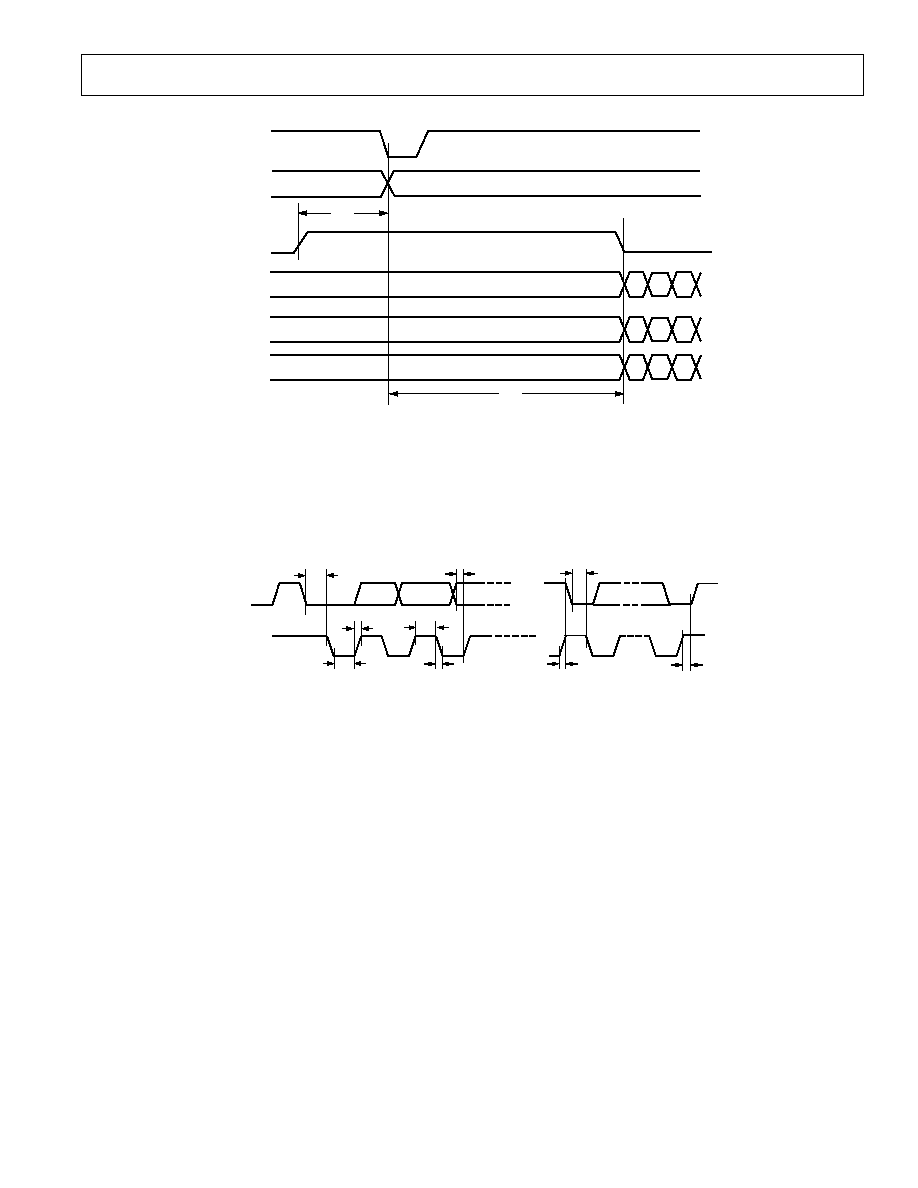
REV. 0
ADV7196A
7
A
MIN
= 16 CLKCYCLES (525P)
A
MIN
= 12 CLKCYCLES (625P)
A
MIN
= 44 CLKCYCLES (1080I)
A
MIN
= 70 CLKCYCLES (720P)
PIXEL
DATA
DV
VSYNC
HSYNC
Y
Y
Y
Y
Cr
Cr
Cr
Cr
Cb
Cb
Cb
Cb
B
A
B
MIN
= 122 CLKCYCLES (525P)
B
MIN
= 132 CLKCYCLES (625P)
B
MIN
= 236 CLKCYCLES (1080I)
B
MIN
= 300 CLKCYCLES (720P)
Figure 4. Input Timing Diagram
t
3
t
2
t
6
t
1
t
7
t
3
t
4
t
8
SDA
SCL
t
5
Figure 5. MPU Port Timing Diagram
REV. 0
ADV7196A
8
CAUTION
ESD (electrostatic discharge) sensitive device. Electrostatic charges as high as 4000 V readily
accumulate on the human body and test equipment and can discharge without detection. Although
the ADV7196A features proprietary ESD protection circuitry, permanent damage may occur on
devices subjected to high-energy electrostatic discharges. Therefore, proper ESD precautions are
recommended to avoid performance degradation or loss of functionality.
WARNING!
ESD SENSITIVE DEVICE
ABSOLUTE MAXIMUM RATINGS
1
V
AA
to GND . . . . . . . . . . . . . . . . . . . . . . . . . . . . . . . . . . . 7 V
Voltage on Any Digital Pin . . . . GND 0.5 V to V
AA
+ 0.5 V
Ambient Operating Temperature (T
A
) . . . . . 40
°C to +85°C
Storage Temperature (T
S
) . . . . . . . . . . . . . . 65
°C to +150°C
Infrared Reflow Soldering (20 secs) . . . . . . . . . . . . . . . 225
°C
Vapor Phase Soldering (1 minute) . . . . . . . . . . . . . . . . 220
°C
I
OUT
to GND
2
. . . . . . . . . . . . . . . . . . . . . . . . . . . . 0 V to V
AA
PIN CONFIGURATION
52 51 50 49 48
43 42 41 40
47 46 45 44
14 15 16 17 18 19 20 21 22 23 24 25 26
1
2
3
4
5
6
7
8
9
10
11
13
12
PIN 1
IDENTIFIER
TOP VIEW
(Not to Scale)
39
38
37
36
35
34
33
32
31
30
29
28
27
ADV7196A
Cr[0]
Cr[1]
Cr[2]
Cr[3]
Cr[4]
Cr[5]
Cr[6]
Cr[7]
Cr[8]
Cr[9]
V
AA
CLKIN
A
GND
GND
Cb/Cr[0]
Cb/Cr[1]
Cb/Cr[2]
Cb/Cr[3]
Cb/Cr[4]
Cb/Cr[5]
Cb/Cr[6]
Cb/Cr[7]
Cb/Cr[8]
Cb/Cr[9]
ALSB
RESET
V
DD
Y[0]
Y[1]
Y[2]
Y[3]
Y[4]
Y[5]
Y[6]
Y[7]
Y[8]
Y[9]
V
DD
GND
V
REF
R
SET
COMP
DAC B
V
AA
DAC A
AGND
DAC C
SDA
SCL
HSYNC/SYNC
VSYNC/TSYNC
DV
ORDERING GUIDE
Model
Temperature Range
Package Description
Package Option
ADV7196AKS
0
°C to 70°C
Plastic Quad Flatpack (MQFP)
S-52
NOTES
1
Stresses above those listed under Absolute Maximum Ratings may cause perma-
nent damage to the device. This is a stress rating only; functional operation of the
device at these or any other conditions above those listed in the operational
sections of this specification is not implied. Exposure to absolute maximum rating
conditions for extended periods may affect device reliability.
2
Analog Output Short Circuit to any Power Supply or Common can be of an
indefinite duration.

REV. 0
ADV7196A
9
PIN FUNCTION DESCRIPTIONS
Pin
Mnemonic
Input/Output
Function
1, 12
V
DD
P
Digital Power Supply
211
Y0Y9
I
10-Bit Progressive Scan/HDTV Input Port for Y Data. Input for G data when
RGB data is input.
13, 52
GND
G
Digital Ground
1423
Cr0Cr9
I
1
0-Bit Progressive Scan/HDTV Input Port for Color Data in 4:4:4 Input Mode.
In 4:2:2 mode this input port is not used. Input port for R data when RGB data
is input.
24, 35
V
AA
P
Analog Power Supply
25
CLKIN
I
Pixel Clock Input. Requires a 27 MHz reference clock for standard operation in
Progressive Scan Mode or a 74.25 MHz (74.1758 MHz) reference clock in
HDTV mode.
26, 33
AGND
G
Analog Ground
27
DV
I
Video Blanking Control Signal Input
28
VSYNC/
I
VSYNC, Vertical Sync Control Signal Input or TSYNC Input Control Signal in
TSYNC
Async Timing Mode
29
HSYNC/
I
HSYNC, Horizontal
Sync Control Signal Input or
SYNC Input Control Signal in
SYNC
Async Timing Mode
30
SCL
I
MPU Port Serial Interface Clock Input
31
SDA
I/O
MPU Port Serial Data Input/Output
32
DAC C
O
Color Component Analog Output of Input Data on Cb/Cr90 Input Pins
34
DAC A
O
Y Analog Output
36
DAC B
O
Color Component Analog Output of Input Data on Cr9Cr0 Input Pins
37
COMP
O
Compensation Pin for DACs. Connect 0.1
µF capacitor from COMP pin to V
AA
.
38
R
SET
I
A 2470
resistor (for input ranges 64940 and 64960; output standards
EIA-770.1EIA-770.3) must be connected from this pin to ground and is used to
control the amplitudes of the DAC outputs. For input ranges 01023 (output
standards RS-170, RS-343A) the R
SET
value must be 2820
.
39
V
REF
I/O
Optional External Voltage Reference Input for DACs or Voltage Reference
Output (1.235 V)
40
RESET
I
This input resets the on-chip timing generator and sets the ADV7196A into
Default Register setting. Reset is an active low signal.
41
ALSB
I
TTL Address Input. This signal sets up the LSB of the MPU address. When this
pin is tied high, the I
2
C filter is activated which reduces noise on the I
2
C interface.
When this pin is tied low, the input bandwidth on the I
2
C interface is increased.
4251
Cb/Cr90
I
1
0-Bit Progressive Scan/HDTV Input Port for Color Data. In 4:2:2 mode the
multiplexed CrCb data must be input on these pins. Input port for B data when
RGB is input.
REV. 0
ADV7196A
10
FUNCTIONAL DESCRIPTION
Digital Inputs
The digital inputs of the ADV7196A are TTL compatible. 30-bit
YCrCb or RGB pixel data in 4:4:4 format or 20-bit YCrCb pixel
data in 4:2:2 format is latched into the device on the rising edge
of each clock cycle at 74.25 MHz or 74.1758 in HDTV mode.
It is also possible to input 3
× 10 bit RGB data in 4:4:4 to the
ADV7196A. It is recommended to input data in 4:2:2 mode to
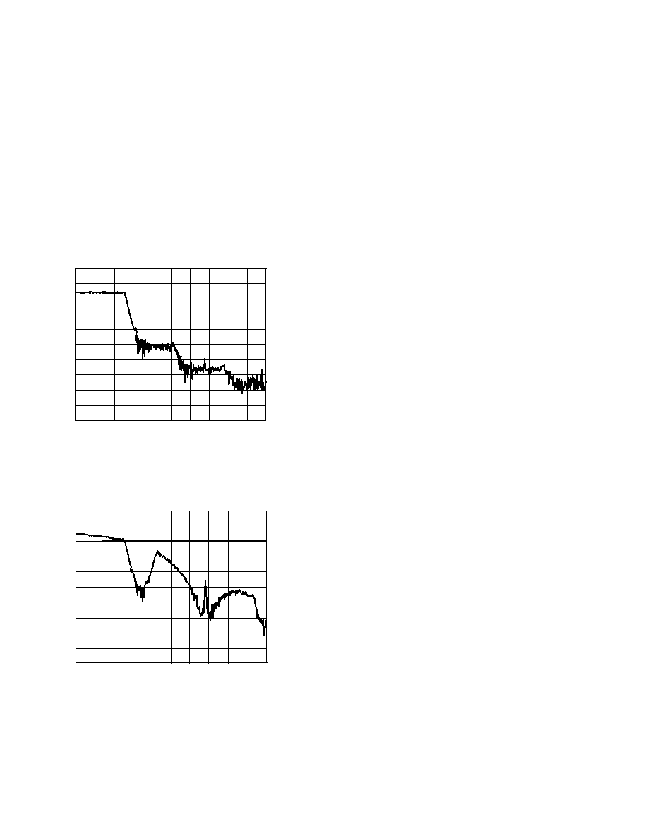
make use of the Chroma SSAFs on the ADV7196A. As can be
seen in the figure below, this filter has a 0 dB pass band response
and prevents signal components being folded back in to the fre-
quency band. In 4:4:4: input mode, the video data is already
interpolated by the external input device and the Chroma SSAFs
of the ADV7196A are bypassed.
RBW 10kHz
VBW 300Hz
SWP 17.0SEC
START 100kHz
STOP
20.00MHz
RL 10.0dBm
10dB/
3.18MHz
ATTEN
10dB
VAVG
1
MKR
0dB
Figure 6. ADV7196A SSAF Response to a 2.5 MHz Chroma
Sweep Using 4:2:2 Input Mode
RBW 10kHz
VBW
300Hz
SWP
17.0SEC
START
100kHz
STOP
20.00MHz
RL 10.0dBm
10dB/
3.12MHz
ATTEN
10dB
VAVG
4
MKR
3.00dB
Figure 7. Conventional Filter Response to a 2.5 MHz Chroma
Sweep Using 4:4:4 Input Mode
Control Signals
The ADV7196A accepts sync control signals accompanied by
valid 4:2:2 or 4:4:4 data. These external horizontal, vertical and
blanking pulses (or EAV/SAV codes) control the insertion of
appropriate sync information into the output signals.
Analog Outputs
The analog Y signal is output on the 11-Bit + Sync DAC A,
the color component analog signals on the 11-Bit DACs B, C
conforming to EIA-770.1 or EIA-770.2 standards in PS mode
or EIA-770.3 in HDTV mode. R
SET
has a value of 2470
(EIA-770.1, EIA-770.2, EIA-770.3), R
LOAD
has a value of 300
.
For RGB outputs conforming to RS-170/RS-343A output standards
R
SET
must have a value of 2820
.
I
2
C Filters
A selectable internal I
2
C filter allows significant noise reduction
on the I
2
C interface. In setting ALSB high, the input bandwidth
on the I
2
C lines is reduced and pulses of less than 50 ns are not
passed to the I
2
C controller. Setting ALSB low allows greater
input bandwidth on the I
2
C lines.
Undershoot Limiter
A limiter can be applied to the Y data before it is applied to the DACs.
Available limit values are 1.5 IRE, 6 IRE, 11 IRE below blank-
ing. This functionality is available in Progressive Scan mode only.
Internal Test Pattern Generator
The ADV7196A can generate a cross-hatch pattern (white lines
against a black background). Additionally, the ADV7196A can
output a uniform color pattern. The color of the lines or uniform
field/frame can be programmed by the user.
Y/CrCb Delay
The Y output and the color component outputs can be delayed
wrt the falling edge of the horizontal sync signal by up to four
clock cycles.
Gamma Correction
Gamma correction may be performed on the luma data. The
user has the choice to use either of two different gamma curves,
A or B. At any one time one of these curves is operational if gamma
correction is enabled. Gamma correction allows the mapping of
the luma data to a user-defined function.
54 MHz Operation
In Progressive Scan mode, it is possible to operate the three out-
put DACs at 54 MHz or 27 MHz. The ADV7196A is supplied
with a 27 MHz clock synced with the incoming data. If required, a
second stage interpolation filter interpolates the data to 54 MHz
before it is applied to the three output DACs. The second stage
interpolation filter is controlled by MR36. After applying a
Reset it is recommended to toggle this bit. Before toggling this bit,
3Ehex must be written to address 09hex.
PROGRAMMABLE SHARPNESS FILTER
Sharpness Filter Mode is applicable to the Y data only in Progres-
sive Scan mode. The desired frequency response can be chosen
by the user in programming the correct value via the I
2
C. The
variation of frequency responses can be seen in the figures on the
following pages.
PROGRAMMABLE ADAPTIVE FILTER CONTROL
If the Adaptive Filter Mode is enabled (Progressive Scan mode only),
it is possible to compensate for large edge transitions on the
incoming Y data. Sensitivity and attenuation are all program-
mable over the I
2
C. For further information refer to Sharpness
Filter Control and Adaptive Filter Control section.
REV. 0
ADV7196A
11
Input/Output Configuration
Table I shows possible input/output configurations when using
the ADV7196A.
Table I.
Input Format
Output
YCrCb Progressive Scan
4:2:2
2
×
4:4:4
1
× or 2×
YCrCb HDTV
4:2:2
1
×
4:4:4
1
×
RGB Progressive Scan
4:4:4
2
×
RGB HDTV
4:4:4
1
×
Async Timing Mode
All Inputs
1
×
10
0
80
40
50
60
70
20
30
10
5
10
15
20
25
0
30
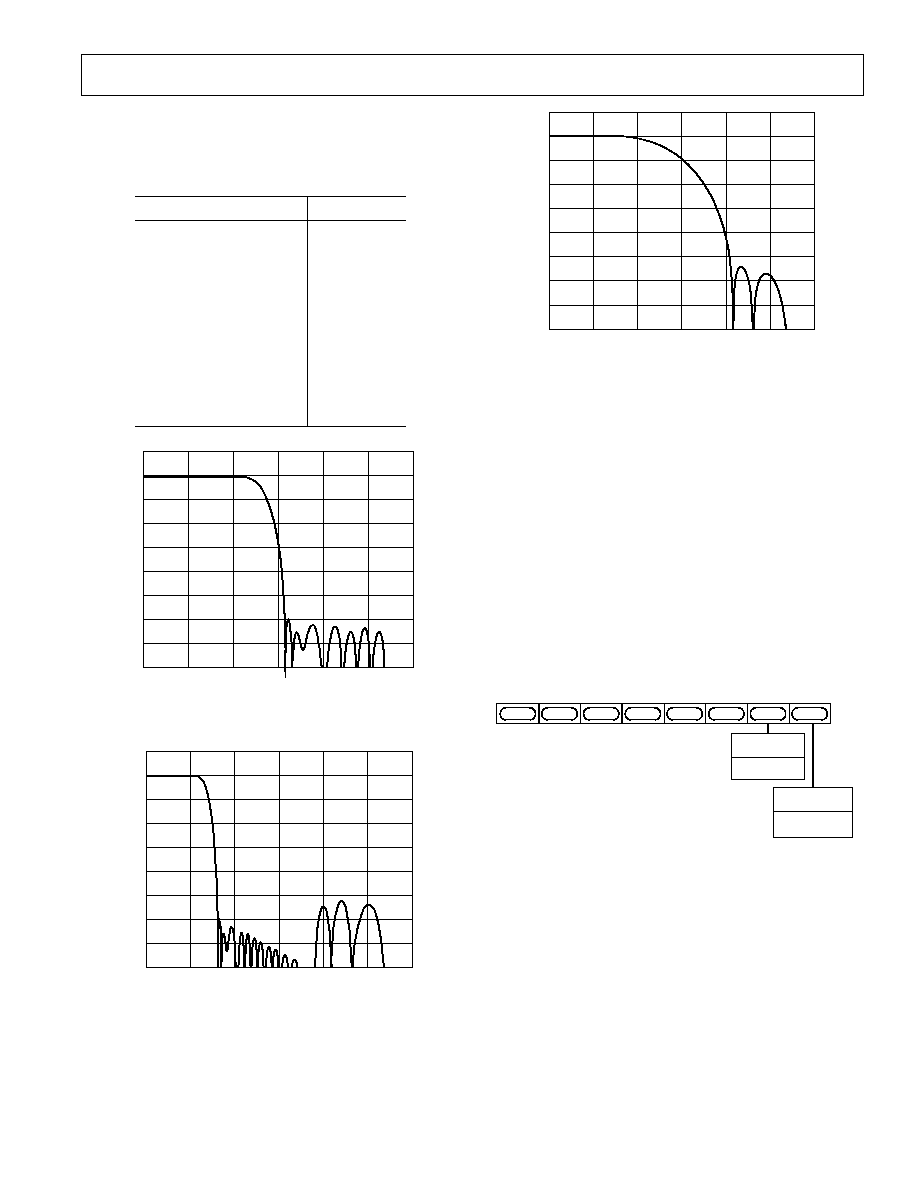
Figure 8. 2
× Interpolation Filter Y-Channel
10
0
80
40
50
60
70
20
30
10
5
10
15
20
25
0
30
Figure 9. Interpolation Filter CrCb Channels for
4:2:2
Input Data
10
0
80
40
50
60
70
20
30
10
5
10
15
20
25
0
30
Figure 10. Interpolation Filter CrCb Channels for
4:4:4
Input Data
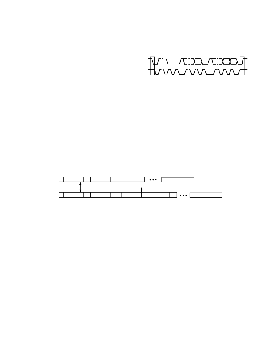
MPU PORT DESCRIPTION
The ADV7196A support a 2-wire serial (I
2
C-compatible) micro-
processor bus driving multiple peripherals. Two inputs, Serial Data
(SDA) and Serial Clock (SCL), carry information between any
device connected to the bus. Each slave device is recognized by a
unique address. The ADV7196A has four possible slave addresses
for both read and write operations. These are unique addresses
for each device and illustrated in Figure 11. The LSB sets either
a read or write operation. Logic Level "1" corresponds to a read
operation while Logic Level "0" corresponds to a write opera-
tion. A1 is set by setting the ALSB pin of the ADV7196A to Logic
Level "0" or Logic Level "1." When ALSB is set to "0," there is
greater input bandwidth on the I
2
C lines, which allows high-
speed data transfers on this bus. When ALSB is set to "1," there
is reduced input bandwidth on the I
2
C lines, which means that
pulses of less than 50 ns will not pass into the I
2
C internal control-
ler. This mode is recommended for noisy systems.
1
X
1
0
1
0
1
A1
ADDRESS
CONTROL
SET UP BY
ALSB
READ/
WRITE
CONTROL
0
WRITE
1
READ
Figure 11. Slave Address
To control the various devices on the bus the following protocol
must be followed. First the master initiates a data transfer by
establishing a Start condition, defined by a high-to-low transi-
tion on SDA while SCL remains high. This indicates that an
address/data stream will follow. All peripherals respond to the
Start condition and shift the next eight bits (7-bit address + R/
W
bit). The bits are transferred from MSB down to LSB. The
peripheral that recognizes the transmitted address responds by
pulling the data line low during the ninth clock pulse. This is
known as an acknowledge bit. All other devices withdraw from
the bus at this point and maintain an idle condition. The idle
condition is where the device monitors the SDA and SCL lines
waiting for the Start condition and the correct transmitted address.
The R/
W bit determines the direction of the data.
REV. 0
ADV7196A
12
A Logic "0" on the LSB of the first byte means that the master will
write information to the peripheral. A Logic "1" on the LSB of
the first byte means that the master will read information from
the peripheral.
The ADV7196A acts as a standard slave device on the bus. The
data on the SDA pin is 8 bits long supporting the 7-bit addresses plus
the R/
W bit. It interprets the first byte as the device address and
the second byte as the starting subaddress. The subaddresses auto-
increment allowing data to be written to or read from the starting
subaddress. A data transfer is always terminated by a Stop con-
dition. The user can also access any unique subaddress register
on a one by one basis without having to update all the registers.
Stop and Start conditions can be detected at any stage during the
data transfer. If these conditions are asserted out of sequence with
normal read and write operations, then these cause an immedi-
ate jump to the idle condition. During a given SCL high period
the user should only issue one Start condition, one Stop condition
or a single Stop condition followed by a single Start condition.
If an invalid subaddress is issued by the user, the ADV7196A will
not issue an acknowledge and will return to the idle condition. If
in autoincrement mode, the user exceeds the highest subaddress
then the following action will be taken:
1. In Read Mode, the highest subaddress register contents will
continue to be output until the master device issues a no-
acknowledge. This indicates the end of a read. A no-acknowledge
condition is where the SDA line is not pulled low on the
ninth pulse.
2. In Write Mode, the data for the invalid byte will be not be
loaded into any subaddress register, a no-acknowledge will
be issued by the ADV7196A and the part will return to the
idle condition.
1
7
8
9
1
7
8
9
1
7
8
9
P
S
START ADDR R/
W ACK SUBADDRESS ACK
DATA
ACK
STOP
SDATA
SCLOCK
Figure 12. Bus Data Transfer
Figure 12 illustrates an example of data transfer for a read
sequence and the Start and Stop conditions.
Figure 13 shows bus write and read sequences.
REGISTER ACCESSES
The MPU can write to or read from all of the registers of the
ADV7196A except the Subaddress Registers, which are write-only
registers. The Subaddress Register determines which register the
next read or write operation accesses.
All communications with the part through the bus begin with an
access to the Subaddress Register. A read/write operation is per-
formed from/to the target address which then increments to the
next address until a Stop command on the bus is performed.
DATA
A(S)
S
SLAVE ADDR A(S)
SUB ADDR
A(S)
LSB = 0
LSB = 1
DATA
A(S) P
S
SLAVE ADDR A(S)
SUB ADDR
A(S) S
SLAVE ADDR
A(S)
DATA
A(M)
A(M)
DATA
P
WRITE
SEQUENCE
READ
SEQUENCE
S = START BIT
A(S) = ACKNOWLEDGE BY SLAVE
A(S) = NO-ACKNOWLEDGE BY SLAVE
P = STOP BIT
A(M) = ACKNOWLEDGE BY MASTER
A(M) = NO-ACKNOWLEDGE BY MASTER
Figure 13. Write and Read Sequence
REV. 0
ADV7196A
13
REGISTER PROGRAMMING
The following section describes the functionality of each register.
All registers can be read from as well as written to unless other-
wise stated.
Subaddress Register (SR7SR0)
The Communications Register is an eight bit write-only register.
After the part has been accessed over the bus and a read/write
operation is selected, the subaddress is set up. The Subaddress
Register determines to/from which register the operation takes place.
Figure 14 shows the various operations under the control of the
Subaddress Register. "0" should always be written to SR7.
Register Select (SR6SR0)
These bits are set up to point to the required starting address.
SR4
SR3
SR2
SR1
SR0
SR7
SR6
SR5
ADDRESS
SR6 SR5
SR4
SR3
SR2
SR1
SR0
00h
0
0
0
0
0
0
0
MODE REGISTER 0
01h
0
0
0
0
0
0
1
MODE REGISTER 1
02h
0
0
0
0
0
1
0
MODE REGISTER 2
03h
0
0
0
0
0
1
1
MODE REGISTER 3
04h
0
0
0
0
1
0
0
MODE REGISTER 4
05h
0
0
0
0
1
0
1
MODE REGISTER 5
06h
0
0
0
0
1
1
0
COLOR Y
07h
0
0
0
0
1
1
1
COLOR CR
08h
0
0
0
1
0
0
0
COLOR CB
09h
0
0
0
1
0
0
1
MODE REGISTER 6
0Ah
0
0
0
1
0
1
0
RESERVED
0Bh
0
0
0
1
0
1
1
RESERVED
0Ch
0
0
0
1
1
0
0
RESERVED
0Eh
0
0
0
1
1
1
0
RESERVED
0Fh
0
0
0
1
1
1
1
RESERVED
10h
0
0
1
0
0
0
0
FILTER GAIN
11h
0
0
1
0
0
0
1
CGMS DATA REGISTER 0
12h
0
0
1
0
0
1
0
CGMS DATA REGISTER 1
13h
0
0
1
0
0
1
1
CGMS DATA REGISTER 2
14h
0
0
1
0
1
0
0
GAMMA CORRECTION REGISTER 0
15h
0
0
1
0
1
0
1
GAMMA CORRECTION REGISTER 1
16h
0
0
1
0
1
1
0
GAMMA CORRECTION REGISTER 2
17h
0
0
1
0
1
1
1
GAMMA CORRECTION REGISTER 3
18h
0
0
1
1
0
0
0
GAMMA CORRECTION REGISTER 4
19h
0
0
1
1
0
0
1
GAMMA CORRECTION REGISTER 5
1Ah
0
0
1
1
0
1
0
GAMMA CORRECTION REGISTER 6
1Bh
0
0
1
1
0
1
1
GAMMA CORRECTION REGISTER 7
1Ch
0
0
1
1
1
0
0
GAMMA CORRECTION REGISTER 8
1Dh
0
0
1
1
1
0
1
GAMMA CORRECTION REGISTER 9
1Eh
0
0
1
1
1
1
0
GAMMA CORRECTION REGISTER 10
1Fh
0
0
1
1
1
1
1
GAMMA CORRECTION REGISTER 11
20h
0
1
0
0
0
0
0
GAMMA CORRECTION REGISTER 12
21h
0
1
0
0
0
0
1
GAMMA CORRECTION REGISTER 13
22h
0
1
0
0
0
1
0
ADAPTIVE FILTER GAIN 1
23h
0
1
0
0
0
1
1
ADAPTIVE FILTER GAIN 2
24h
0
1
0
0
1
0
0
ADAPTIVE FILTER GAIN 3
25h
0
1
0
0
1
0
1
ADAPTIVE FILTER THRESHOLD A
26h
0
1
0
0
1
1
0
ADAPTIVE FILTER THRESHOLD B
27h
0
1
0
0
1
1
1
ADAPTIVE FILTER THRESHOLD C
ADV7196A SUBADDRESS REGISTER
ZERO SHOULD
BE WRITTEN
HERE
SR7
Figure 14. Subaddress Registers in Progressive Scan Mode
SR4
SR3
SR2
SR1
SR0
SR7
SR6
SR5
ADDRESS
SR6 SR5
SR4
SR3
SR2
SR1
SR0
00h
0
0
0
0
0
0
0
MODE REGISTER 0
01h
0
0
0
0
0
0
1
MODE REGISTER 1
02h
0
0
0
0
0
1
0
MODE REGISTER 2
03h
0
0
0
0
0
1
1
MODE REGISTER 3
04h
0
0
0
0
1
0
0
MODE REGISTER 4
05h
0
0
0
0
1
0
1
MODE REGISTER 5
06h
0
0
0
0
1
1
0
COLOR Y
07h
0
0
0
0
1
1
1
COLOR CR
08h
0
0
0
1
0
0
0
COLOR CB
ADV7196A SUBADDRESS REGISTER
ZERO SHOULD
BE WRITTEN
HERE
SR7
Figure 15. Subaddress Registers in HDTV Mode
REV. 0
ADV7196A
14
PROGRESSIVE SCAN MODE
MODE REGISTER 0
MR0 (MR07MR00)
(Address (SR4SR0) = 00H)
Figure 16 shows the various operations under the control of
Mode Register 0.
MR0 BIT DESCRIPTION
Output Standard Selection (MR00MR01)
These bits are used to select the output levels for the ADV7196A.
If EIA-770.2 (MR0100 = "00") is selected the output levels will
be: 0 mV for blanking level, 700 mV for peak white for the Y
channel,
±350 mV for Pr, Pb outputs and 300 mV for Sync. Sync
insertion on the Pr, Pb channels is optional.
If EIA-770.1 (MR0100 = "01") is selected the output levels will
be: 0 mV for blanking level, 714 mV for peak white for the Y chan-
nel,
±350 mV for Pr, Pb outputs and 286 mV for Sync. Optional
sync insertion on the Pr, Pb channels is not possible.
If Full I/P Range (MR0100 = "10") is selected the output levels
will be 0 mV for blanking level, 700 mV for peak white for the Y
channel,
±350 mV for Pr, Pb outputs and 300 mV for Sync. Sync
insertion on the Pr, Pb channels is optional. This mode is used
for RS-170, RS-343A standard output compatibility. Refer to
Appendix for output level plots.
Input Control Signals (MR02MR03)
These control bits are used to select whether data is input with
external horizontal, vertical and blanking sync signals or if the data
is input with embedded EAV/SAV codes.
An Asynchronous timing mode is also available using TSYNC,
SYNC and DV as input control signals. These control signals
have to be programmed by the user.
Figure 17 shows an example of how to program the ADV7196A to
accept a different high definition standard but SMPTE293M,
SMPTE274M, SMPTE296M or ITU-R.BT1358 standard.
Input Standard (MR04)
Select between 525p progressive scan input or 625p progressive
scan input.
Reserved (MR05)
A "0" must be written to this bit.
DV Polarity (MR06)
This control bit allows to select the polarity of the DV input
control signal to be either active high or active low. This is in
order to facilitate interfacing from I to P Converters which use
an active low blanking signal output.
Macrovision (MR07)
To enable Macrovision this bit must be set to "1."
MR01
MR07
MR02
MR04
MR05
MR06
MR07
0
DISABLED
1
ENABLED
MACROVISION
MR03
MR00
ZERO MUST
BE WRITTEN
TO THIS BIT
MR05
MR06
0
ACTIVE HIGH
1
ACTIVE LOW
DV POLARITY
MR04
0
525P
1
625P
INPUT STANDARD
MR03 MR02
HSYNC\VSYNC/DV
EAV/SAV
TSYNC/
SYND/DV
RESERVED
INPUT CONTROL SIGNALS
MR01 MR00
0
0
EIA-770.2
0 1
EIA-770.1
1
0
FULL I/P RANGE
1
1
RESERVED
OUTPUT STANDARD SELECTION
0
1
0
1
0
0
1
1
Figure 16. Mode Register 0
REV. 0
ADV7196A
15
Table II must be followed when programming the control sig-
nals in Async Timing Mode.
Table II. Truth Table
SYNC
TSYNC
DV
1 > 0
0
0 or 1
50% Point of Falling Edge of
Tri-Level Horizontal Sync
Signal, A
0
0 > 1
0 or 1
25% Point of Rising Edge of
Tri-Level Horizontal Sync
Signal, B
0 > 1
0 or 1
0
50% Point of Falling Edge of
Tri-Level Horizontal Sync
Signal, C
1
0 or 1
0 > 1
50% Start of Active Video, D
1
0 or 1
1 > 0
50% End of Active Video, E
A
B
C
D
E
CLK
SYNC
TSYNC
DV SET
MR06 = 1
PROGRAMMABLE
INPUT TIMING
ANALOG
OUTPUT
ACTIVE VIDEO
HORIZONTAL SYNC
66
81
66
243
1920
Figure 17. Async Timing Mode--Programming Input Control Signals for SMPTE295M Compatibility
VIDEO
OUTPUT
HSYNC
525
VSYNC
DV
1
12
13
42
43
Figure 18. DV Input Control Signal in Relation to Video Output Signal
REV. 0
ADV7196A
16
VBI Open (MR14)
This bit enables or disables the facility of VBI data insertion during
the Vertical Blanking Interval.
For this purpose Lines 13 to 42 of each frame can be used for VBI
when SMPTE293M standard is used, or Lines 6 to 43 when
ITU-R.BT1358 standard is used
.
Undershoot Limiter (MR15MR16)
This control limits the Y signal to a programmable level in the active
video region.
Available limit levels are 1.5 IRE, 6 IRE, 11 IRE.
Note that this facility is only available when Interpolation is enabled
(MR36 = "1")
.
Sharpness Filter (MR17)
This control bit enables or disables the Sharpness Filter mode. This
bit must be set to "1" for any values programmed into the Filter
Gain 1 Register to take effect. It must also be set to "1" when
Adaptive Filter mode is used.
Refer to Sharpness Filter control and Adaptive Filter control section.
6IRE
100IRE
0IRE
40IRE
Figure 19. Undershoot Limiter, Programmed to 6 IRE
MODE REGISTER 1
MR1 (MR17MR10)
(Address (SR4SR0) = 01H)
Figure 20 shows the various operations under the control of Mode
Register 1.
MR1 BIT DESCRIPTION
Pixel Data Enable (MR10)
When this bit is set to "0," the pixel data input to the ADV7196A
is blanked such that a black screen is output from the DACs. When
this bit is set to "1," pixel data is accepted at the input pins and
the ADV7196A outputs the standard set in "Output Standard
Selection" (MR0100). This bit must be set to "1" to enable out-
put of the test pattern signals.
Input Format (MR11)
It is possible to input data in 4:2:2 format or at 4:4:4 format at
27 MHz.
Test Pattern Enable (MR12)
Enables or disables the internal test pattern generator.
Test Pattern Hatch/Frame (MR13)
If this bit is set to "0," a cross-hatch test pattern is output from the
ADV7196A (for example, in SMPTE293M 11 horizontal and 11
vertical white lines, four pixels wide are displayed against a black
background). The cross-hatch test pattern can be used to test
monitor convergence.
If this bit is set to "1," a uniform colored frame/field test pattern
is output from the ADV7196A.
The color of the lines or the frame/field is by default white but can
be programmed to be any color using the Color Y, Color Cr,
Color Cb registers.
MR11
MR17
MR12
MR14
MR15
MR16
MR17
0
DISABLED
1
ENABLED
SHARPNESS
FILTER
MR13
MR10
MR14
0
DISABLED
1
ENABLED
VBI OPEN
MR12
0
DISABLED
1
ENABLED
TEST PATTERN
ENABLE
MR10
0
DISABLED
1
ENABLED
PIXEL DATA
ENABLE
MR16 MR15
0
0
DISABLED
0
1
11IRE
1
0
6IRE
1
1
1.5IRE
UNDERSHOOT
LIMITER
MR13
0
HATCH
1
FIELD/FRAME
TEST PATTERN
HATCH/FRAME
MR11
0
4:4:4 YCRCB
1
4:2:2 YCRCB
INPUT FORMAT
Figure 20. Mode Register 1
REV. 0
ADV7196A
17
MODE REGISTER 2
MR1 (MR27MR20)
(Address (SR4SR0) = 02H)
Figure 22 shows the various operations under the control of Mode
Register 2.
MR2 BIT DESCRIPTION
Y Delay (MR20MR22)
This control bit delays the Y signal with respect to the falling edge
of the horizontal sync signal by up to four pixel clock cycles.
Figure 21 demonstrates this facility
.
Color Delay (MR23MR25)
This control allows delay of the color signals with respect to the
falling edge of the horizontal sync signal by up to four pixel clock
cycles. Figure 21 demonstrates this facility
.
CGMS Enable (MR26)
When this bit is set to "1," CGMS data is inserted on Line 41 in
525p mode. The CGMS conforms: to CGMS-A EIA-J CPR1204-1,
Transfer Method of Video ID information using vertical blanking
interval (525p System), March 1998 and IEC61880, 1998, video
systems (525/60)--video and accompanied data using the vertical
blanking interval--analogue interface.
The CGMS data bits are programmed into the CGMS Data
Registers 02. For more information refer to CGMS Data
Registers section
.
CGMS CRC (MR27)
This bit enables the automatic Cyclic Redundancy Check when
CGMS is enabled.
MAX DELAY
NO DELAY
NO DELAY
MAX DELAY
PrPb DELAY
Y DELAY
Y OUTPUT
PrPb OUTPUTS
Figure 21. Y and Color Delay
MR21
MR27
MR22
MR24
MR25
MR23
MR20
MR26
MR27
0
DISABLED
1
ENABLED
CGMS CRC
MR26
0
DISABLED
1
ENABLED
CGMS ENABLE
MR25
MR24
MR23
0
0
0
0 PCLK
0
0
1
1 PCLK
0
1
0
2 PCLK
0
1
1
3 PCLK
1
0
0
4 PCLK
COLOR DELAY
MR22
MR21
MR20
0
0
0
0 PCLK
0
0
1
1 PCLK
0
1
0
2 PCLK
0
1
1
3 PCLK
1
0
0
4 PCLK
Y DELAY
Figure 22. Mode Register 2
REV. 0
ADV7196A
18
MODE REGISTER 4
MR4 (MR47MR40)
(Address (SR4SR0) = 04H)
Figure 24 shows the various operations under the control of Mode
Register 4.
MR4 BIT DESCRIPTION
Timing Reset (MR40)
Toggling MR40 from low to high and low again resets the inter-
nal horizontal and vertical timing counters.
MODE REGISTER 5
MR5 (MR57MR50)
(Address (SR4SR0) = 05H)
Figure 25 shows the various operations under the control of
Mode Register 5.
MR5 BIT DESCRIPTION
Reserved (MR50)
This bit is reserved for the revision code
.
RGB Mode (MR51)
When RGB mode is enabled (MR51 = "1") the ADV7196A accepts
unsigned binary RGB data at its input port. This control is also
available in Async Timing Mode
.
Sync on PrPb (MR52)
By default the color component output signals Pr, Pb do not
contain any horizontal sync pulses. They can be inserted when
MR52 = "1." This facility is only available when Output Standard
Selection has been set to EIA-770.2 (MR0100 = "00") or Full
Input Range (MR0100 = "10").
This control is not available in RGB mode
.
MODE REGISTER 3
MR3 (MR37MR30)
(Address (SR4SR0) = 03H)
Figure 23 shows the various operations under the control of Mode
Register 3.
MR3 BIT DESCRIPTION
HDTV Enable (MR30)
When this bit is set to "1" the ADV7196A reverts to HDTV mode
(refer to HDTV mode section). When set to "0" the ADV7196A
is set up in Progressive Scan Mode (PS Mode)
.
Reserved (MR31MR32)
A "0" must be written to these bits
.
DAC A Control (MR33)
Setting this bit to "1" enables DAC A, otherwise this DAC is
powered down
.
DAC B Control (MR34)
Setting this bit to "1" enables DAC B, otherwise this DAC is
powered down
.
DAC C Control (MR35)
Setting this bit to "1" enables DAC C, otherwise this DAC is
powered down
.
Interpolation (MR36)
This bit enables the second stage interpolation filters. When this
bit is enabled (MR36 = "1"). data is send at 54 MHz to the DAC
output stage. After Reset it is recommended to toggle this bit.
Before toggling this bit 3Ehex must be written to address 09hex
to guarantee correct operations
.
Reserved (MR37)
A zero must be written to this bit
.
MR37
MR32
MR34
MR36
ZERO MUST BE
WRITTEN TO
THIS BIT
MR37
MR34
0
POWER-DOWN
1
NORMAL
DAC B CONTROL
MR35
MR36
0
DISABLE
1
ENABLE
INTERPOLATION
MR35
0
POWER-DOWN
1
NORMAL
DAC C CONTROL
MR33
ZERO MUST BE
WRITTEN TO
THIS BIT
MR32
MR31
MR30
0
DISABLE
1
ENABLE
HDTV ENABLE
MR30
MR33
0
POWER-DOWN
1
NORMAL
DAC A CONTROL
ZERO MUST BE
WRITTEN TO
THIS BIT
MR31
Figure 23. Mode Register 3
MR47
MR42
MR44
MR46
ZERO MUST BE
WRITTEN TO
THESE REGISTERS
MR47MR41
MR45
MR43
MR41
MR40
MR40
TIMING RESET
Figure 24. Model Register 4
REV. 0
ADV7196A
19
Color Output Swap (MR53)
By default DAC B is configured as the Pr output and DAC C
as the Pb output. In setting this bit to "1" the DAC outputs can
be swapped around so that DAC B outputs Pb and DAC C
outputs Pr. Table III demonstrates this in more detail. This control
is also available in RGB mode
.
Table III. Relationship Between Color Input Pixel Port,
MR53 and DAC B, DAC C Outputs
In 4:4:4 Input Mod
e
Color Data
Analog Output
Input on Pins
MR53
Signal
Cr90
0
DAC B
Cb/Cr90
0
DAC C
Cr90
1
DAC C
Cb/Cr90
1
DAC B
In 4:2:2 Input Mod
e
Color Data
Analog Output
Input on Pins
MR53
Signal
Cr90
0 or 1
Not Operational
Cb/Cr90
0
DAC C (Pb)
Cb/Cr90
1
DAC C (Pr)
Gamma Curve (MR54)
This bit selects which of the two programmable gamma curves is to
be used. When setting MR54 to "0," the gamma correction curve
selected is Curve A. Otherwise Curve B is selected. Each curve
will have to be programmed by the user as explained in the Gamma
Correction Registers section
.
Gamma Correction (MR55)
To enable Gamma Correction and therefore activate the gamma
curve programmed by the user, this bit must be set to "1." Otherwise
the programmable Gamma Correction facility is bypassed. Pro-
gramming of the gamma correction curves is explained in the
Gamma Correction Registers section
.
Adaptive Mode Control (MR56)
For this control to be effective, Adaptive Filter Control must be
enabled (MR57 = "1") as well as the Sharpness Filter (MR17 =
"1"). For filter plots refer to Sharpness Filter Control and
Adaptive Filter Control section
.
Adaptive Filter Control (MR57)
This bit enables the Adaptive Filter Control when set to "1."
Sharpness Filter must be enabled as well (MR17 = "1"). The
Adaptive Filter Controls is explained in more detail under
Sharpness Filter Control and Adaptive Filter Control section
.
COLOR Y
CY (CY7CY0)
(Address (SR4SR0) = 06H
CY7
CY6
CY5
CY4
CY3
CY2
CY1
CY0
CY7CY0
COLOR Y VALUE
Figure 26. Color Y Register
COLOR CR
CCR (CCR7CCR0)
(Address (SR4SR0) = 07H
CCR7
CCR6
CCR5
CCR4
CCR3
CCR2
CCR1
CCR0
CCR7CCR0
COLOR CR VALUE
Figure 27. Color Cr Register
COLOR CB
CCB (CCB7CCB0)
(Address (SR4SR0) = 08H)
CCB7
CCB6
CCB5
CCB4
CCB3
CCB2
CCB1
CCB0
CCB7CCB0
COLOR CB VALUE
Figure 28. Color Cb Register
These three 8-bit-wide registers are used to program the output
color of the internal test pattern generator, be it the lines of the
cross-hatch pattern or the uniform field test pattern and are
available in PS mode and HDTV mode.
The standard used for the values for Y and the color difference
signals to obtain white, black and the saturated primary and
complementary colors conforms to the ITU-R BT 601-4 standard.
COLOR OUTPUT
SWAP
RESERVED FOR
REVISION CODE
MR50
MR57
MR56
MR55
MR54
MR53
MR52
MR51
MR50
0
MODE A
1
MODE B
MR56
ADAPTIVE MODE
CONTROL
MR57
ADAPTIVE FILTER
CONTROL
0
DISABLE
1
ENABLE
MR55
GAMMA
CORRECTION
0 DISABLE
1 ENABLE
SYNC ON PrPb
MR52
0
DISABLE
1
ENABLE
0
CURVE A
1
CURVE B
MR54
GAMMA CURVE
RGB MODE
MR51
0
DISABLE
1
ENABLE
MR53
0 DAC B = Pr
1 DAC C = Pr
Figure 25. Mode Register 5
REV. 0
ADV7196A
20
The Table IV shows sample color values to be programmed into
the color registers when Output Standard Selection is set to
EIA-770.2 (MR0100 = "00")
.
Table IV. Sample Color Values for EIA 770.2 Output
Standard Selectio
n
Sample
Color Y
Color Cr
Color Cb
Color
Value
Value
Value
White
235 (EB)
128 (80)
128 (80)
Black
16 (10)
128 (80)
128 (80)
Red
81 (51)
240 (F0)
90 (5A)
Green
145 (91)
34 (22)
54 (36)
Blue
41 (29)
110 (6E)
240 (F0)
Yellow
210 (D2)
146 (92)
16 (10)
Cyan
170 (AA)
16 (10)
166 (A6)
Magenta
106 (6A)
222 (DE)
202 (CA)
MODE REGISTER 6
MR6 (MR67MR60)
(Address (SR4SR0) = 09H)
Figure 29 shows the various operations under the control of
Mode Register 6
.
MR6 BIT DESCRIPTION
MR67MR60
The value 3Ehex must be written to this register before the
PLL is reset (reset MR36) to guarantee correct operation of
the ADV7196A.
MR67
ZERO MUST BE
WRITTEN TO
THIS BIT
MR60
MR66
MR65
MR64
MR63
MR62
MR61
MR60
ONE MUST BE
WRITTEN TO
THIS BIT
MR62
ONE MUST BE
WRITTEN TO
THIS BIT
MR64
ZERO MUST BE
WRITTEN TO
THIS BIT
MR66
ONE MUST BE
WRITTEN TO
THIS BIT
MR61
ONE MUST BE
WRITTEN TO
THIS BIT
MR63
ONE MUST BE
WRITTEN TO
THIS BIT
MR65
ZERO MUST BE
WRITTEN TO
THIS BIT
MR67
Figure 29. Mode Register 6
CGMS DATA REGISTERS 20
CGMS2 (CGMS27CGMS20)
(Address (SR4SR0) = 13H)
This 8-bit-wide register contains the last four CGMS data bits,
(C16C19) of the CGMS data stream.
CGMS23CGMS20
CGMS2
CGMS27 CGMS26
CGMS25
CGMS24
CGMS23
CGMS22
CGMS21 CGMS20
CGMS27CGMS24
ZERO MUST BE WRITTEN
TO THESE BITS
Figure 30. CGMS2 Data Register
CGMS1 (CGMS17CGMS10)
(Address (SR4SR0) = 12H)
This 8-bit-wide register contains (C8C15) of the CGMS
data stream.
CGMS17CGMS10
CGMS1
CGMS17 CGMS16
CGMS15
CGMS14
CGMS13
CGMS12
CGMS11 CGMS10
Figure 31. CGMS1 Data Register
CGMS0 (CGMS07CGMS00)
(Address (SR4SR0) = 11H)
This 8-bit-wide register contains the first eight CGMS data
bits, (C0C7) of the CGMS data stream.
CGMS07CGMS00
CGMS0
CGMS07 CGMS06
CGMS05
CGMS04
CGMS03
CGMS02
CGMS01 CGMS00
Figure 32. CGMS0 Data Register
CRC SEQUENCE
21.2 s 0.22 s
22T
REF
C0
C1
C2
C3
C4
C5
C6
C7
C8
C9 C10 C11 C12 C13 C14 C15 C16 C17 C18 C19
700mV
(70 10)%
0mV
300mV
BIT1 BIT2................................................................................................................................................BIT20
5.8 s 0.15 s
6T
T = 1/(fH 33) = 963ns
fH = HORIZONTAL SCAN FREQUENCY
T 30ns
Figure 33. CGMS Waveform
REV. 0
ADV7196A
21
The response of the curve is programmed at seven predefined
locations. In changing the values at these locations the gamma
curve can be modified. Between these points linear interpolation
is used to generate intermediate values. Considering the curve to
have a total length of 256 points, the seven locations are at: 32,
64, 96, 128, 160, 192, 224.
Location 0, 16, 240, and 255 are fixed and can not be changed.
For the length of 16 to 240 the gamma correction curve has to be
calculated as below:
y = x
where:
y = gamma corrected output.
x = linear input signal
.
= gamma power factor.
To program the gamma correction registers, the seven values for
y have to be calculated using the following formula:
y
n
= [
x(n16)
/(240 16)]
(240) 16) + 16
where:
x
(n16)
= Value for x along x-axis at points:
n
= 32, 64, 96, 128, 160, 192, or 224.
y
n
= Value for y along the y-axis, which has to be written into
the gamma correction register.
Example:
y
32
= [(16/22
4)0
.
5 2 24] + 16 = 76*
y
64
= [(48/22
4)0
.
5 224] + 16 =120*
y
96
= [(80/22
4)0
.
5 224] + 16 = 150*
y
128
= [(112/22
4)0
.
5 224] + 16 = 147*
*Rounded to the nearest integer.
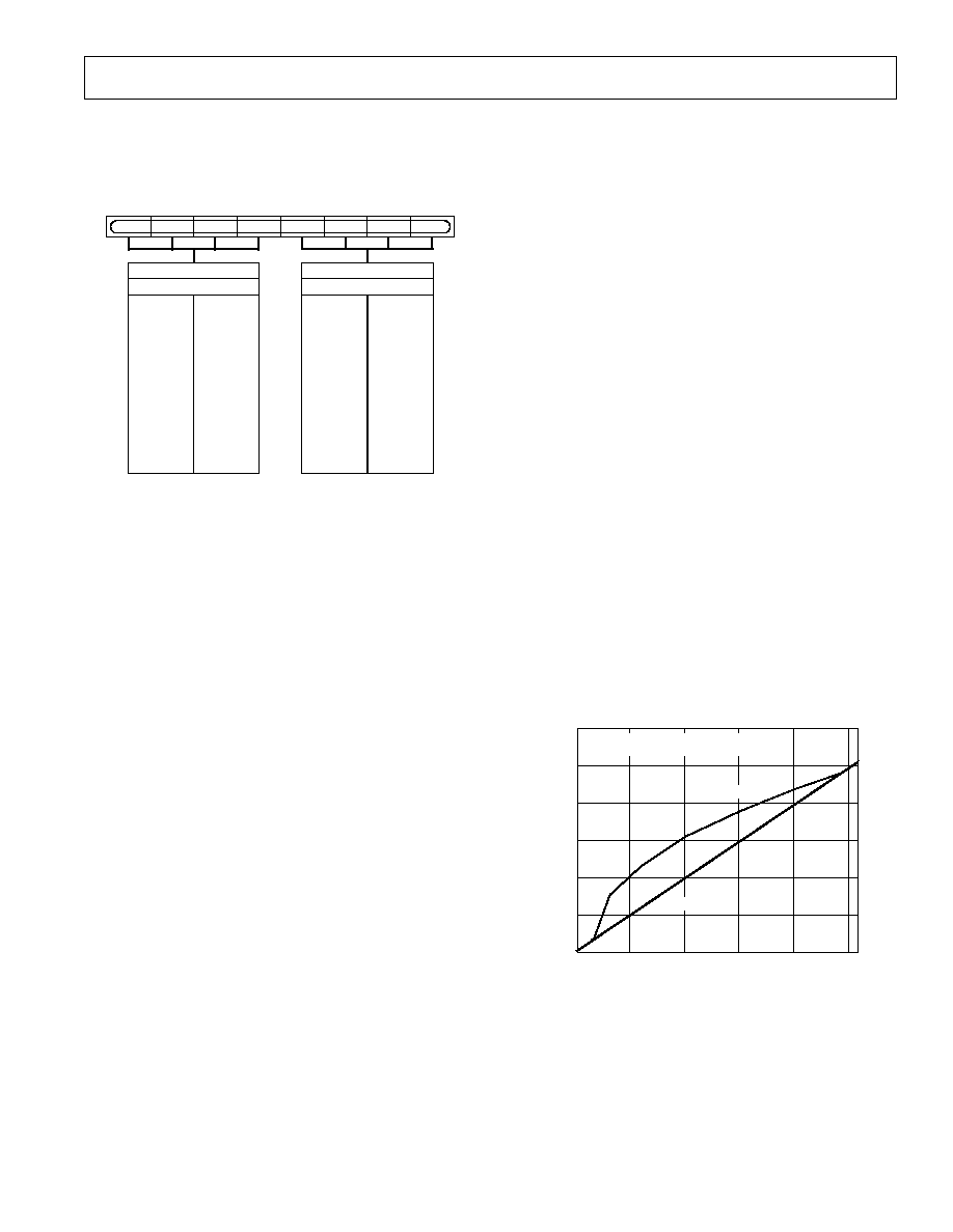
The above will result in a gamma curve shown below, assuming a
ramp signal as an input.
250
200
150
100
50
0
300
SIGNAL OUTPUT
SIGNAL INPUT
0.5
GAMMA CORRECTION BLOCK OUTPUT
TO A RAMP INPUT
GAMMA-CORRECTED AMPLITUDE
0
50
100
150
200
250
LOCATION
Figure 35. Signal Input (Ramp) and Signal Output for
Gamma 0.5
FILTER GAIN
FG (FG7FG0)
(Address (SR4SR0) = 10H)
Figure 34 shows the various operations under the control of the
Filter Gain register
.
FG7
FG6
FG5
FG4
FG3
FG2
FG1
FG0
FG7FG4
FILTER GAIN B
0000
0
0001
1
0010
2
0011
3
0100
4
0101
5
0110
6
0111
7
1000
8
1001
7
1010
6
1011
5
1100
4
1101
3
1110
2
1111
1
FG3FG0
FILTER GAIN A
0000
0
0001
1
0010
2
0011
3
0100
4
0101
5
0110
6
0111
7
1000
8
1001
7
1010
6
1011
5
1100
4
1101
3
1110
2
1111
1
Figure 34. Filter Gain Register
FG BIT DESCRIPTION
Filter Gain A (FG3FG0)
These bits are used to program the gain A value, which varies
from response 8 to response +7 and are applied to Filter A.
Filter Gain B (FG4FG7)
These bits are used to program the gain B value, which varies
from response 8 to response +7 and are applied to Filter B.
Refer to Sharpness Filter Control and Adaptive Filter Control
section for more detail.
GAMMA CORRECTION REGISTERS 013
(GAMMA CORRECTION 013)
(Address (SR5SR0) = 14H21H)
The Gamma Correction Registers are fourteen 8-bit-wide register.
They are used to program the gamma correction Curves A and B.
Generally, gamma correction is applied to compensate for the
nonlinear relationship between signal input and brightness level
output (as perceived on the CRT). It can also be applied wherever
nonlinear processing is used.
Gamma correction uses the function:
Signal
OUT
= (Signal
IN
)
where
= gamma power factor.
Gamma correction is performed on the luma data only.
The user has the choice to use two different curves, Curve A or
Curve B. At any one time only one of these curves can be used.
REV. 0
ADV7196A
22
250
200
150
100
50
0
300
SIGNAL OUTPUTS
SIGNAL INPUT
0.5
GAMMA CORRECTION BLOCK OUTPUT
TO A RAMP INPUT FOR VARIOUS GAMMA VALUES
GAMMA-CORRECTED AMPLITUDE
0
50
100
150
200
250
LOCATION
0.3
1.5
1.8
Figure 36. Signal Input (Ramp) and Selectable Gamma
Output Curves
The gamma curves shown above are examples only, any user
defined curve is acceptable in the range of 16240
.
SHARPNESS FILTER CONTROL AND ADAPTIVE
FILTER CONTROL
There are three Filter modes available on the ADV7196A: one
Sharpness Filter mode and two Adaptive Filter modes.
SHARPNESS FILTER MODE
To enhance or attenuate the Y signal in the frequency ranges shown
in Figure 37, the following register settings must be used:
Sharpness Filter must be enabled (MR17 = "1") and Adaptive
Filter Control must be disabled (MR57 = "0").
To select one of the 256 individual responses, the according gain
values for each filter, which range from 8 to +7, must be pro-
grammed into the Filter Gain register
.
ADAPTIVE FILTER MODE
The Adaptive Filter Threshold A, B, C registers, the Adaptive
Filter Gain 1, 2, 3 registers and the Filter Gain register are used
in Adaptive Filter mode. To activate the Adaptive Filter control,
Sharpness Filter must be enabled (MR17 = "1") and Adaptive
Filter Control must be enabled (MR57 = "1").
The derivative of the incoming signal is compared to the three pro-
grammable threshold values: Adaptive Filter Threshold A, B, C.
The edges can then be attenuated with the settings in Adaptive
Filter Gain 1, 2, 3 registers and Filter Gain register.
According to the settings of the Adaptive Mode control (MR56),
there are two Adaptive Filter Modes available:
1. Mode A: is used when Adaptive Filter Mode (MR56) is set
to "0." In this case, Filter B (LPF) will be used in the adaptive
filter block. Also, only the programmed values for Gain B in
the Filter Gain, Adaptive Filter Gain 1, 2, 3 are applied when
needed. The Gain A values are fixed and can not be changed.
2. Mode B: is used when Adaptive Filter Mode (MR56) is set to
"1." In this mode a cascade of Filter A and Filter B is used. Both
settings for Gain A and Gain B in the Filter Gain, Adaptive
Filter Gain 1, 2, 3 become active when needed
.
FREQUENCY MHz
MA
GNITUDE
1.5
1.4
1.3
1.2
1.1
1.0
0.9
0.8
0.7
0.6
0.5
0
2
4
6
8
10
12
14
8
7
6
5
4
3
2
1
0
1
2
3
4
5
6
7
FREQUENCY MHz
MA
GNITUDE
1.5
1.4
1.3
1.2
1.1
1.0
0.9
0.8
0.7
0.6
0.5
0
2
4
6
8
10
12
14
8
7
6
5
4
3
2
1
0
1
2
3
4
5
6
7
SHARPNESS AND ADAPTIVE FILTER CONTROL MODE
INPUT SIGNAL: STEP
FREQUENCY MHz
MA
GNITUDE RESPONSE
Linear Scale
1.6
1.5
1.4
1.3
1.2
1.1
1.0
0
2
4
6
8
10
12
14
FREQUENCY RESPONSE IN SHARPNESS FILTER MODE
WITH K
A
= 3 and K
B
= 7
Figure 37. Sharpness and Adaptive Filter Control Mode
REV. 0
ADV7196A
23
ADAPTIVE FILTER GAIN 1
AFG1 (AFG1)70
(Address (SR5SR0) = 22H)
This 8-bit-wide register is used to program the gain applied to signals
which lie above Adaptive Filter Threshold A but are smaller than
Adaptive Filter Threshold B.
Gain A and Gain B values vary from 8 to +7. The individual
responses are shown in the figures below.
Settings for (AFG1)30 have no effect unless Adaptive Mode Con-
trol is set to Mode B (MR56 = "1").
AFG13AFG10
GAIN A
AFG17
AFG16
AFG15
AFG14
AFG13
AFG12
AFG11
AFG10
AFG17AFG14
GAIN B
Figure 38. Adaptive Filter Gain 1 Register
ADAPTIVE FILTER GAIN 2
AFG2 (AFG2)70
(Address (SR5SR0) = 23H)
This 8-bit-wide register is used to program the gain applied
to signals which lie above Adaptive Filter Threshold B but are
smaller than Adaptive Filter Threshold C.
Gain A and Gain B values vary from 8 to +7. The individual
responses are shown in the figures below.
Settings for (AFG2)30 have no effect unless Adaptive Mode Con-
trol is set to Mode B (MR56 = "1").
AFG23AFG20
GAIN A
AFG27
AFG26
AFG25
AFG24
AFG23
AFG22
AFG21
AFG20
AFG27AFG24
GAIN B
Figure 39. Adaptive Filter Gain 2 Register
ADAPTIVE FILTER GAIN 3
AFG3 (AFG3)70
(Address (SR5SR0) = 24H)
This 8-bit-wide register is used to program the gain applied to signals
which lie above Adaptive Filter Threshold C
Gain A and Gain B values vary from 8 to +7. The individual
responses are shown in the figures below.
Settings for (AFG3)30 have no effect unless Adaptive Mode Con-
trol is set to Mode B (MR56 = "1").
The gain applied to signals which lie below Adaptive Threshold A
are programmed in the Filter Gain register.
At any one time only one of the following registers is active: AFG1,
AFG2, AFG3, FG. The gain values can be preprogrammed and
become active whenever the threshold conditions for the accord-
ing register is met. To program the Adaptive Filter Gain registers
the source register settings are used as for the Filter Gain register
.
AFG33AFG30
GAIN A
AFG37
AFG36
AFG35
AFG34
AFG33
AFG32
AFG31
AFG30
AFG37AFG34
GAIN B
Figure 40. Adaptive Filter Gain 3 Register
ADAPTIVE FILTER THRESHOLD A
AFTA (AFTA)70
(Address (SR5SR0) = 25H)
This 8-bit-wide register is used to program the threshold value for
small edges. The recommended programmable threshold range is
from 16235, although any value in the range of 0255 can be used.
AFTA7AFTA0
ADAPTIVE FILTER
THRESHOLD A
AFTA7
AFTA6
AFTA5
AFTA4
AFTA3
AFTA2
AFTA1
AFTA0
Figure 41. Adaptive Filter Threshold A Register
ADAPTIVE FILTER THRESHOLD B
AFTB (AFTB)70
(Address (SR5SR0) = 26H)
This 8-bit-wide register is used to program the threshold value for
medium edges and has priority over Adaptive Threshold A. The
recommended programmable threshold range is from 16235,
although any value in the range of 0255 can be used.
AFTB7AFTB0
ADAPTIVE FILTER
THRESHOLD B
AFTB7
AFTB6
AFTB5
AFTB4
AFTB3
AFTB2
AFTB1
AFTB0
Figure 42. Adaptive Filter Threshold B Register
ADAPTIVE FILTER THRESHOLD C
AFTC (AFTC)70
(Address (SR5SR0) = 27H)
This 8-bit-wide register is used to program the threshold value
for large edges and has priority over Adaptive Threshold A and B.
The recommended programmable threshold range is from 16235,
although any value in the range of 0255 can be used.
AFTC7AFTC0
ADAPTIVE FILTER
THRESHOLD C
AFTC7
AFTC6
AFTC5
AFTC4
AFTC3
AFTC2
AFTC1
AFTC0
Figure 43. Adaptive Filter Threshold C Register
REV. 0
ADV7196A
24
SHARPNESS FILTER AND ADAPTIVE FILTER
APPLICATION EXAMPLES
Sharpness Filter Application
The sharpness filter can be used to enhance or attenuate the Y
video output signal.
The following register settings were used to achieve the results
shown in the figures below:
Input data was generated by an external signal source
.
Table V.
Address
Register Setting
00hex
Mode Register 0
40hex
01hex
Mode Register 1
81hex
02hex
Mode Register 2
00hex
03hex
Mode Register 3
78hex
04hex
Mode Register 4
00hex
05hex
Mode Register 5
00hex
09hex
Mode Register 6
3Ehex
10hex
Filter Gain
00hex
(a)
10hex
Filter Gain
08hex
(b)
10hex
Filter Gain
04hex
(c)
10hex
Filter Gain
40hex
(d)
10hex
Filter Gain
80hex
(e)
10hex
Filter Gain
22hex
(f)
CH1
T
R2
R4
1
(B)
(C)
(A)
TEK RUN
T
TRIG'D
500mV
M 4.00 s
REF4
500mV
4.00 s
9.99976ms
T
CH1
ALL FIELDS
(a)
CH1
T
R2
R1
1
(E)
(F)
(D)
TEK RUN
T
TRIG'D
500mV
M 4.00 s
REF2
500mV
4.00 s
9.99976ms
T
CH1
ALL FIELDS
(b)
Figure 44. Sharpness Filter Control with Different Gain Settings for Filter Gain
The effect of the sharpness filter can also be seen when using the
internally generated cross hatch pattern
:
Table VI.
Address
Register Setting
00hex
Mode Register 0
00hex
01hex
Mode Register 1
85hex
02hex
Mode Register 2
00hex
03hex
Mode Register 3
38hex
04hex
Mode Register 4
00hex
05hex
Mode Register 5
00hex
09hex
Mode Register 6
3Ehex
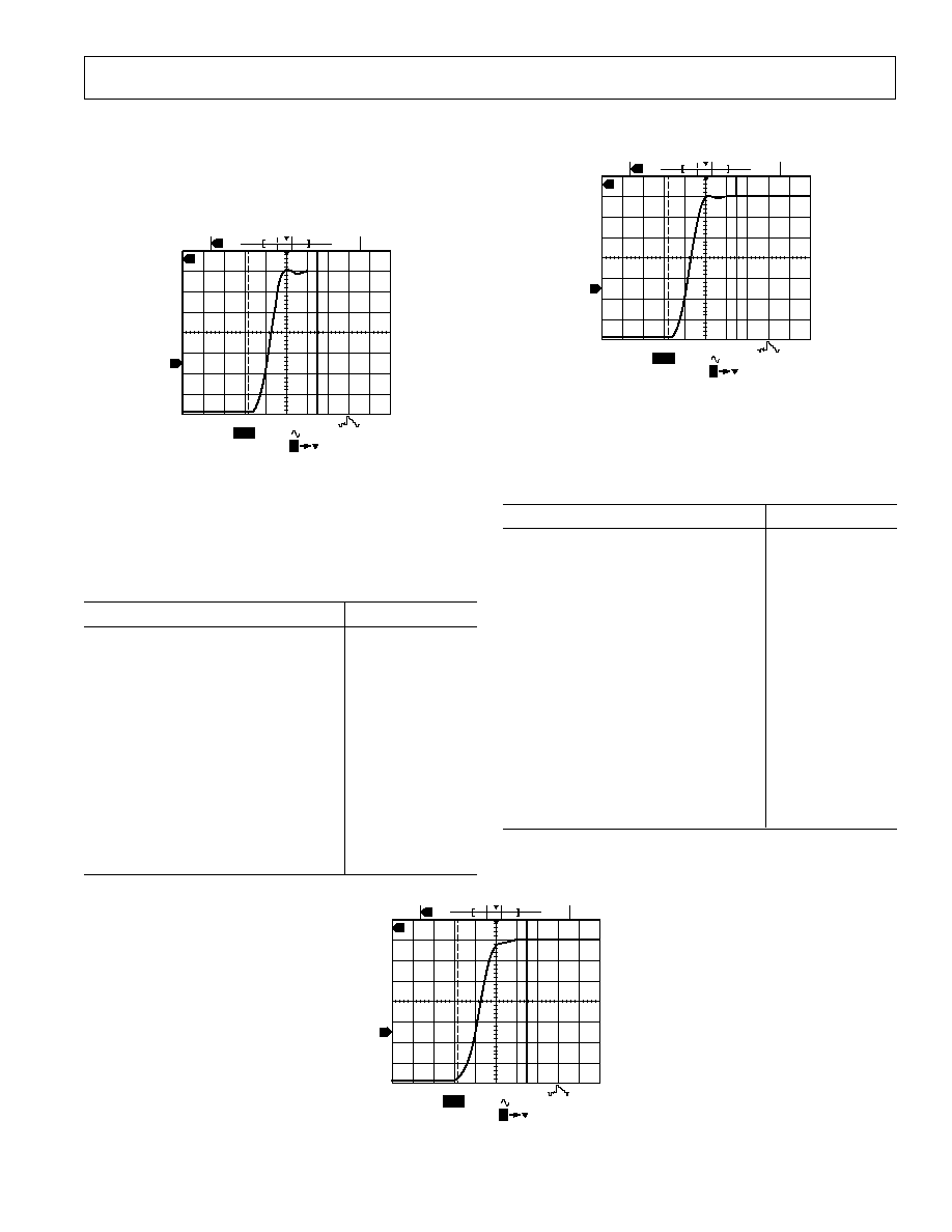
REV. 0
ADV7196A
25
In toggling MR17 (Sharpness Filter Enable/Disable) and setting
the Filter Gain register value to 99hex it can be seen that the line
contours of the cross hatch pattern change their sharpness
.
Adaptive Filter Control Application
The figure below shows a typical signal to be processed by the
Adaptive Filter Control block.
T
4
TEK RUN
T
TRIG'D
M 100ns
12.8222ms
T
CH4
ALL FIELDS
CH4
100mV
Figure 45. Input Signal to Adaptive Filter Control
The following register settings where used to obtain the
results shown in the figure below, i.e., to remove the ringing
on the Y signal:
Input data was generated by an external signal source.
Table VII.
Address
Register Setting
00hex
Mode Register 0
40hex
01hex
Mode Register 1
81hex
02hex
Mode Register 2
00hex
03hex
Mode Register 3
78hex
04hex
Mode Register 4
00hex
05hex
Mode Register 5
80hex
09hex
Mode Register 6
3Ehex
10hex
Filter Gain
00hex
22hex
Adaptive Filter Gain 1
AChex
23hex
Adaptive Filter Gain 2
9Ahex
24hex
Adaptive Filter Gain 3
88hex
25hex
Adaptive Filter Threshold A
28hex
26hex
Adaptive Filter Threshold B
3Fhex
27hex
Adaptive Filter Threshold C
64hex
The figure below shows the output signal when changing the Adap-
tive Filter mode to Mode B (MR56 = "1").
T
4
TEK RUN
T
TRIG'D
M 100ns
12.8222ms
T
CH4
ALL FIELDS
CH4
100mV
Figure 46. Output Signal from Adaptive Filter Control
The Adaptive Filter control can also be demonstrated using the
internally generated crosshatch test pattern and toggling the Adap-
tive Filter Control bit (MR57) using the following register settings:
Table VIII.
Address
Register Setting
00hex
Mode Register 0
40hex
01hex
Mode Register 1
85hex
02hex
Mode Register 2
00hex
03hex
Mode Register 3
78hex
04hex
Mode Register 4
00hex
05hex
Mode Register 5
80hex
06hex
Color Y
6Chex
07hex
Color Cr
52hex
08hex
Color Cb
52hex
09hex
Mode Register 6
3Ehex
10hex
Filter Gain
00hex
22hex
Adaptive Filter Gain 1
AChex
23hex
Adaptive Filter Gain 2
9Ahex
24hex
Adaptive Filter Gain 3
88hex
25hex
Adaptive Filter Threshold A
28hex
26hex
Adaptive Filter Threshold B
3Fhex
27hex
Adaptive Filter Threshold C
64hex
T
4
TEK RUN
T
TRIG'D
M 100ns
12.8222ms
T
CH4
ALL FIELDS
CH4
100mV
Figure 47. Output Signal from Adaptive Filter Control
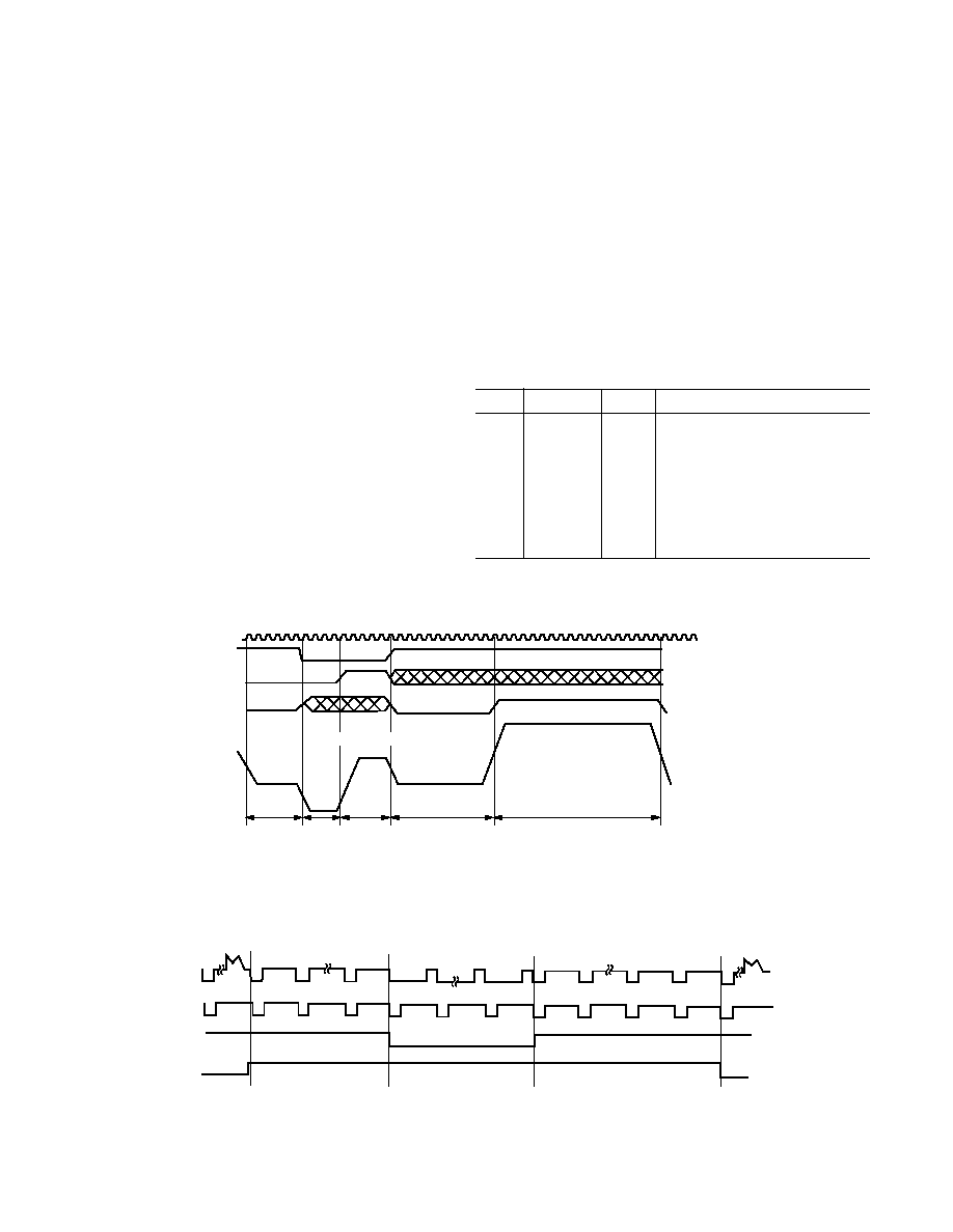
REV. 0
ADV7196A
26
HDTV MODE
MODE REGISTER 0
MR0 (MR07MR00)
(Address (SR4SR0) = 00H)
Figure 50 shows the various operations under the control of Mode
Register 0.
HEXMR0 BIT DESCRIPTION
Output Standard Selection (MR00MR01)
These bits are used to select the output levels from the ADV7196A.
If EIA 770.3 (MR0100 = "00") is selected, the output levels will be:
0 mV for blanking level, 700 mV for peak white (Y channel),
±350 mV for Pr, Pb outputs and 300 mV for tri-level sync.
If Full Input Range (MR0100 = "10") is selected, the output
levels will be 700 mV for peak white for the Y channel,
±350 mV
for Pr, Pb outputs and 300 mV for Sync. This mode is used for
RS-170, RS-343A standard output compatibility.
Sync insertion on the Pr, Pb channels is optional.
For output levels, refer to the Appendix
.
Input Control Signals (MR02MR03)
These control bits are used to select whether data is input with
external horizontal, vertical and blanking sync signals or if the data
is input with embedded EAV/SAV code An Asynchronous timing
mode is also available using TSYNC,
SYNC and DV as input
control signals. These timing control signals have to be programmed
by the user.
Figure 48 shows an example of how to program the ADV7196A
to accept a different high definition standard but SMPTE293M,
SMPTE274M, SMPTE296M or ITU-R.BT1358 standard
.
Reserved (MR04)
A "0" must be written to this bit
.
Input Standard (MR05)
Select between 1080i or 720p input
.
DV Polarity (MR06)
This control bit allows to select the polarity of the DV input control
signal to be either active high or active low
.
Reserved (MR07)
A "0" must be written to this bit
.
Table IX. Truth Table
SYNC TSYNC
DV
1 > 0
0
0 or 1
50% Point of Falling Edge of
Tri-Level Horizontal Signal, A
0
0 > 1
0 or 1
25% Point of Rising Edge of
Tri-Level Horizontal Signal, B
0 > 1
0 or 1
0
50% Point of Falling Edge of
Tri-Level Horizontal Signal, C
1
0 or 1
0 > 1
50% Start of Active Video, D
1
0 or 1
1 > 0
50% End of Active Video, E
CLK
SYNC
TSYNC
DV SET
MR06 = `1'
PROGRAMMABLE
INPUT TIMING
ANALOG
OUTPUT
A
B
C
D
E
243
ACTIVE VIDEO
1920
66
66
81
HORIZONTAL SYNC
Figure 48. Async Timing Mode--Programming Input Control Signals for SMPTE295M Compatibility
7
VIDEO
OUTPUT
HSYNC
525
VSYNC
DV
1
12
13
42
43
Figure 49. DV Input Control Signal in Relation to Video Output Signal
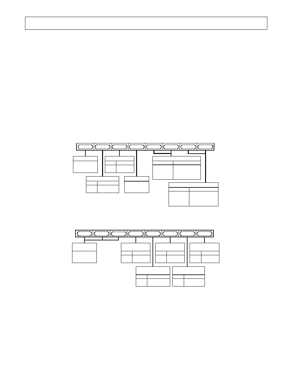
REV. 0
ADV7196A
27
MODE REGISTER 1
MR1 (MR17MR10)
(Address (SR4-SR0) = 01H)
Figure 51 shows the various operations under the control of Mode
Register 1.
MR1 BIT DESCRIPTION
Pixel Data Enable (MR10)
When this bit is set to "0," the pixel data input to the ADV7196A
is blanked such that a black screen is output from the DACs. When
this bit is set to "1," pixel data is accepted at the input pins and
the ADV7196A outputs to the standard set in "Output Standard
Selection" (MR0100). This bit also must be set to "1" to enable
output pattern signals
.
Input Format (MR11)
It is possible to input data in 4:2:2 format or in 4:4:4
HDTV format
.
Test Pattern Enable (MR12)
Enables or disables the internal test pattern generator
.
Test Pattern Hatch/Frame (MR13)
If this bit is set to "0," a cross-hatch test pattern is output from
the ADV7196A. The cross-hatch test pattern can be used to test
monitor convergence.
If this bit is set to "1," a uniform colored frame/field test pattern
is output from the ADV7196A.
The color of the lines or the frame/field is by default white but
can be programmed to be any color using the Color Y, Color
Cr, Color Cb registers
.
VBI Open (MR14)
This bit enables or disables the facility of VBI data insertion during
the Vertical Blanking Interval.
For this purpose Lines 720 in 1080i and Lines 625 in 720p can
be used for VBI data insertion
.
Reserved (MR15MR17)
A "0" must be written to these bits
.
MR01
MR07
MR02
MR04
MR06
MR07
ZERO MUST BE
WRITTEN TO
THIS BIT
MR03
MR00
MR03 MR02
0
0
HSYNC/VSYNC/DV
0
1
EAV/SAV
1
0
TSYNC/
SYNC/DV
1
1
RESERVED
INPUT CONTROL SIGNALS
MR05
MR06
0
ACTIVE HIGH
1
ACTIVE LOW
DV POLARITY
MR05
0
1080I
1
720P
INPUT STANDARD
MR04
ZERO MUST BE
WRITTEN TO
THIS BIT
MR01 MR00
0
0
EIA770.3
0
1
RESERVED
1
0
FULL I/P RANGE
1
1
RESERVED
OUTPUT STANDARDS SELECTION
Figure 50. Mode Register 0
MR11
MR17
MR12
MR14
MR16
MR13
MR10
MR14
0
DISABLED
1
ENABLED
VBI OPEN
MR12
0
DISABLED
1
ENABLED
TEST PATTERN
ENABLE
MR10
0
DISABLED
1
ENABLED
PIXEL DATA
ENABLE
MR13
0
HATCH
1
FIELD/FRAME
TEST PATTERN
HATCH/FRAME
MR11
0
4:4:4 YCRCB
1
4:2:2 YCRCB
INPUT FORMAT
MR15
MR17MR15
ZERO MUST BE
WRITTEN TO
THESE BITS
Figure 51. Mode Register 1
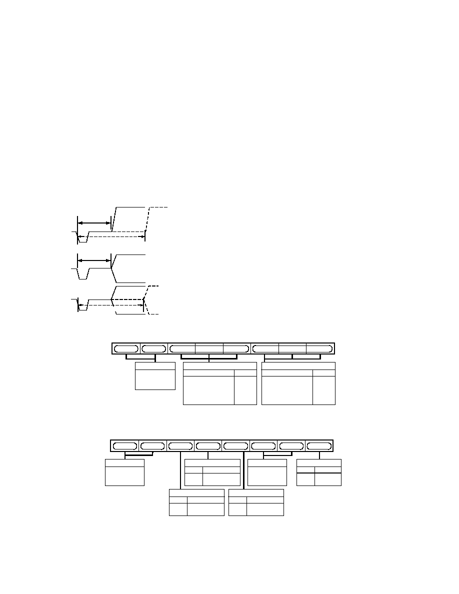
REV. 0
ADV7196A
28
MODE REGISTER 2
MR1 (MR27MR20)
(Address (SR4SR0) = 02H)
Figure 53 shows the various operations under the control of Mode
Register 2.
MR2 BIT DESCRIPTION
Y Delay (MR20MR22)
With these bits it is possible to delay the Y signal with respect to
the falling edge of the horizontal sync signal by up to four pixel
clock cycles. Figure 52 demonstrates this facility.
Color Delay (MR23MR25)
With theses bits it is possible to delay the color signals with respect
to the falling edge of the horizontal sync signal by up to four pixel
clock cycles. Figure 52 demonstrates this facility.
Reserved (MR26MR27)
A "0" must be written to these bits
.
MAX DELAY
NO DELAY
NO DELAY
MAX DELAY
PrPb DELAY
Y DELAY
Y OUTPUT
PrPb OUTPUTS
Figure 52. Y and Color Delay
MODE REGISTER 3
MR3 (MR37MR30)
(Address (SR4-SR0) = 03H)
Figure 54 shows the various operations under the control of Mode
Register 3
.
MR3 BIT DESCRIPTION
HDTV Enable (MR30)
When this bit is set to "1" the ADV7196A reverts to HDTV
mode. When set to "0" the ADV7196A reverts to Progressive
Scan mode (PS mode).
Reserved (MR31MR32)
A "0" must be written to these bits.
DAC A Control (MR33)
Setting this bit to "1" enables DAC A, otherwise this DAC is
powered down.
DAC B Control (MR34)
Setting this bit to "1" enables DAC B, otherwise this DAC is
powered down.
DAC C Control (MR35)
Setting this bit to "1" enables DAC C, otherwise this DAC is
powered down.
Reserved (MR36MR37)
A "0" must be written to these bits.
MR21
MR27
MR22
MR24
MR25
MR23
MR20
MR26
MR25
MR24
MR23
0
0
0
0 PCLK
0
0
1
1 PCLK
0
1
0
2 PCLK
0
1
1
3 PCLK
1
0
0
4 PCLK
COLOR DELAY
MR22
MR21
MR20
0
0
0
0 PCLK
0
0
1
1 PCLK
0
1
0
2 PCLK
0
1
1
3 PCLK
1
0
0
4 PCLK
Y DELAY
MR27MR26
ZERO MUST BE
WRITTEN TO
THESE BITS
Figure 53. Mode Register 2
MR37
MR32
MR34
MR36
ZERO MUST BE
WRITTEN TO
THESE BITS
MR37MR36
MR34
0
POWER-DOWN
1
NORMAL
DAC B CONTROL
MR35
MR35
0
POWER-DOWN
1
NORMAL
DAC C CONTROL
MR33
ZERO MUST BE
WRITTEN TO
THESE BITS
MR32MR31
MR31
MR30
0
DISABLE
1
ENABLE
HDTV ENABLE
MR30
MR33
0
POWER-DOWN
1
NORMAL
DAC A CONTROL
Figure 54. Mode Register 3
REV. 0
ADV7196A
29
MODE REGISTER 4
MR4 (MR47MR40)
(Address (SR4SR0) = 04H)
Figure 55 shows the various operations under the control of Mode
Register 4.
MR4 BIT DESCRIPTION
Timing Reset (MR40)
Toggling MR40 from low to high and low again resets the inter-
nal horizontal and vertical timing counters
.
MODE REGISTER 5
MR5 (MR57MR50)
(Address (SR4SR0) = 05H)
Figure 56 shows the various operations under the control of Mode
Register 5.
MR5 BIT DESCRIPTION
Reserved (MR50)
These bit is reserved for the revision code
.
RGB Mode (MR51)
When RGB mode is enabled (MR51 = "1") the ADV7196A accepts
unsigned binary RGB data at its input port. This control is also
available in Async Timing Mode
.
Sync on PrPb (MR52)
By default the color component output signals Pr, Pb do not contain
any horizontal sync pulses. If required they can be inserted when
MR52 = "1." This control is not available in RGB mode
.
Color Output Swap (MR53)
By default DAC B is configured as the Pr output and DAC C as
the Pb output. In setting this bit to "1" the DAC outputs can be
swapped around so that DAC B outputs Pb and DAC C outputs
Pr. Table X demonstrates this in more detail.
Reserved (MR54MR57)
"0" must be written to these bits.
Table X. Relationship Between Input Pixel Port, MR53
and DAC B, DAC C Outputs
In 4:4:4 Input Mod
e
Color Data
Analog Output
Input on Pins
MR53
Signal
Cr90
0
DAC B
Cb/Cr90
0
DAC C
Cr90
1
DAC C
Cb/Cr90
1
DAC
B
In 4:2:2 Input Mod
e
Color Data
Analog Output
Input on Pins
MR53
Signal
Cr90
0 or 1
Not Operational
Cb/Cr90
0
DAC C (Pb)
Cb/Cr90
1
DAC C (Pr)
MR47
MR42
MR44
MR46
ZERO MUST BE
WRITTEN TO
THESE BITS
MR47MR41
MR45
MR43
MR41
MR40
MR40
TIMING RESET
Figure 55. Mode Register 4
MR57
MR52
MR56
MR57MR54
ZERO MUST BE
WRITTEN TO
THESE BITS
MR55
MR53
MR51
MR50
MR54
MR53
0
DAC B = Pr
1
DAC C = Pr
COLOR OUTPUT
SWAP
MR52
0
DISABLE
1
ENABLE
SYNC ON PrPb
MR51
0
DISABLE
1
ENABLE
RGB MODE
RESERVED FOR
REVISION CODE
MR50
Figure 56. Mode Register 5
REV. 0
ADV7196A
30
DAC TERMINATION AND LAYOUT CONSIDERATIONS
Voltage Reference
The ADV7196A contains an on-board voltage reference. The
V
REF
pin is normally terminated to
V
AA
through a 0.1
µF capacitor
when the internal
V
REF
is used. Alternatively, the ADV7196A
can be used with an external
V
REF
(AD589).
Resistor
R
SET
is connected between the
R
SET
pin and AGND and
is used to control the full-scale output current and therefore the
DAC voltage output levels. For full-scale output
R
SET
must have
a value of 2470
.
R
LOAD
has a value of 300
. When an input
range of 01023 is selected the value of
R
SET
must be 2820
.
The ADV7196A has three analog outputs, corresponding to Y, Pr,
Pb video signals. The DACs must be used with external buffer circuits
in order to provide sufficient current to drive an output device.
Suitable op amps are the AD8009, AD8002, AD8001, or AD8057.
To calculate the output full-scale current and voltage the follow-
ing equations should be used:
V
OUT
=
I
OUT
R
LOAD
I
OUT
= [V
REF
k]/R
SET
where:
k = 5.66 [for input ranges 64940, 64960, output standards
EIA770.13]
k = 6.46 [for input ranges 01023, output standard RS170/343A]
V
REF
= 1.235 V
PC BOARD LAYOUT CONSIDERATIONS
The ADV7196A is optimally designed for lowest noise performance,
both radiated and conducted noise. To complement the excellent
noise performance of the ADV7196A, it is imperative that great
care be given to the PC board layout.
The layout should be optimized for lowest noise on the ADV7196A
power and ground lines. This can be achieved by shielding the
digital inputs and providing good decoupling. The lead length
between groups of
V
AA
and AGND and
V
DD
and DGND pins
should be kept as short as possible to minimized inductive ringing.
It is recommended that a four-layer printed circuit board is used.
With power and ground planes separating the layer of the signal
carrying traces of the components and solder side layer. Placement
of components should consider to separate noisy circuits, such
as crystal clocks, high-speed logic circuitry and analog circuitry.
There should be a separate analog ground plane (AGND) and
a separate digital ground plane (GND).
Power planes should encompass a digital power plane (V
DD
) and
a analog power plane (V
AA
). The analog power plane should contain
the DACs and all associated circuitry, and the
V
REF
circuitry.
The digital power plane should contain all logic circuitry. The analog
and digital power planes should be individually connected to the
common power plane at one single point through a suitable filter-
ing device, such as a ferrite bead.
300
5k
5k
MPU BUS
4.7k
V
DD
POWER SUPPLY DECOUPLING
FOR EACH POWER SUPPLY GROUP
ALSB
DV
RESET
CLKIN
R
SET
SDA
SCL
DAC A
V
DD
VSYNC/TSYNC
ADV7196A
UNUSED
INPUTS
SHOULD BE
GROUNDED
DAC B
100
HSYNC/SYNC
DAC C
27MHz, 74.25MHz OR
74.1758MHz CLOCK
4.7k
4.7 F
6.3V
300
300
100
2.47k OR
2.82k
10nF
0.1 F
Y OUTPUT
Pr (V) OUTPUT
Pb (U) OUTPUT
V
REF
GND
13, 52
AGND
26, 33
Y0Y9
Cr0Cr9
Cb/Cr0Cb/Cr9
0.1 F
10nF
0.1 F
24, 35
1, 12
V
DD
V
AA
COMP
V
AA
V
AA
V
DD
V
DD
V
DD
Figure 57. Circuit Layout
REV. 0
ADV7196A
31
ADV7196A
DAC A
DAC B
DAC C
AD8057
+5V
+5V
75 COAX
75
AD8057
5V
0.1 F
10 F
+5V
75 COAX
75
AD8057
5V
+5V
75 COAX
75
PROGRESSIVE
SCAN
MONITOR
75
LPF
LPF
LPF
0.1 F
10 F
0.1 F
10 F
0.1 F
10 F
0.1 F
10 F
0.1 F
10 F
75
75
Figure 58. Output Buffer and Optional Filter
DAC output traces on a PCB should be treated as transmission
lines. It is recommended that the DACs be placed as close as
possible to the output connector, with the analog output traces
being as short as possible (less than 3 inches). The DAC termina-
tion resistors should be placed as close as possible to the DAC
outputs and should overlay the PCB's ground plane. As well as
minimizing reflections, short analog output traces will reduce noise
pickup due to neighboring digital circuitry
.
Supply Decoupling
Noise on the analog power plane can be further reduced by the
use of decoupling capacitors.
Optimum performance is achieved by the use of 0.1
µF ceramic
capacitors. Each of group of
V
AA
or
V
DD
pins should be indi-
vidually decoupled to ground. This should be done by placing
the capacitors as close as possible to the device with the capaci-
tor leads as short as possible, thus minimizing lead inductance
.
Digital Signal Interconnect
The digital signal lines should be isolated as much as possible
from the analog outputs and other analog circuitry. Digital signal
lines should not overlay the analog power plane.
Due to the high clock rates used, long clock lines to the ADV7196A
should be avoided to minimize noise pickup. Any active pull-up
termination resistors for the digital inputs should be connected
to the digital power plane and not the analog power plane
.
Analog Signal Interconnect
The ADV7196A should be located as close as possible to the output
connectors thus minimizing noise pickup and reflections due to
impedance mismatch.
For optimum performance, the analog outputs should each have
a source termination resistance to ground of 75
. This termina-
tion resistance should be as close as possible to the ADV7196A
to minimize reflections.
Any unused inputs should be tied to ground
.
Video Output Buffer and Optional Output Filter
Output buffering is necessary in order to drive output devices
,
such as progressive scan or HDTV monitors
.
Analog Devices produces a range of suitable op amps for this
application. Suitable op amps would be the AD8009, AD8002,
AD8001, or AD8057. More information on line driver buffering
circuits is given in the relevant op amp data sheets.
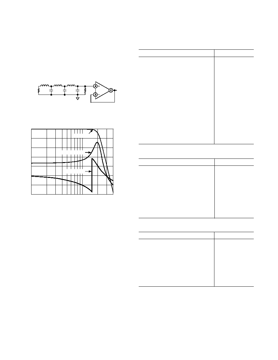
REV. 0
ADV7196A
32
REGISTER SETTINGS
Table XI. Register Settings on Power-U
p
Address
Register Setting
00hex
Mode Register 0
00hex
01hex
Mode Register 1
00hex
02hex
Mode Register 2
00hex
03hex
Mode Register 3
38hex
04hex
Mode Register 4
00hex
05hex
Mode Register 5
00hex
06hex
Color Y
A0hex
07hex
Color CR
80hex
08hex
Color Cb
80hex
09hex
Mode Register 6
00hex
10hex
Filter Gain
00hex
22hex
Adaptive Filter Gain 1
AChex
23hex
Adaptive Filter Gain 2
9Ahex
24hex
Adaptive Filter Gain 3
88hex
25hex
Adaptive Filter Threshold A
28hex
26hex
Adaptive Filter Threshold B
3Fhex
27hex
Adaptive Filter Threshold C
64he
x
Table XII. Internal Colorbars (Hatch), Progressive Scan Mod
e
Address
Register Setting
00hex
Mode Register 0
00hex
01hex
Mode Register 1
05hex
02hex
Mode Register 2
00hex
03hex
Mode Register 3
38hex
04hex
Mode Register 4
00hex
05hex
Mode Register 5
00hex
06hex
Color Y
xxhex
07hex
Color CR
xxhex
08hex
Color Cb
xxhex
09hex
Mode Register 6
3Ehe
x
Table XIII. Internal Colorbars (Field), HDTV Scan Mod
e
Address
Register Setting
00hex
Mode Register 0
00hex
01hex
Mode Register 1
0Dhex
02hex
Mode Register 2
00hex
03hex
Mode Register 3
39hex
04hex
Mode Register 4
00hex
05hex
Mode Register 5
00hex
06hex
Color Y
xxhex
07hex
Color CR
xxhex
08hex
Color Cb
xxhex
An optional analog reconstruction LPF might be required as an
antialias filter if the ADV7196A is connected to a device that
requires this filtering.
The Eval ADV7196A/7EB evaluation board uses the ML6426
Microlinear IC, which provides buffering and low-pass filtering
for progressive scan applications.
The Eval ADV7196A/7EB Rev B and Rev C evaluation board
uses the AD8057 as a buffer and a 6th order LPF.
AD8057
600R
18pF
2.2 H
22pF
10 H
6.8pF
6.8 H
600R
Figure 59. Example for Output Filter: PS Mode/
2x Oversampling
0
1M
5
10
15
20
25
30
35
2
3
4
5
6 7 8 9
10M
FREQUENCY Hz
2
3
4
498
63n
398
54n
298
45n
198
36n
97.6
27n
0
18n
102
9n
202
0n
MAGNITUDE (dB)
PHASE (DEG)
GROUP DELAY (SEC)
Figure 60. Frequency Response for Filter Current in
Above Figure
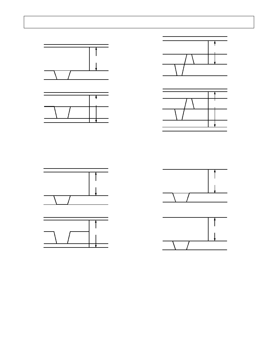
REV. 0
ADV7196A
33
940
64
ACTIVE
VIDEO
700mV
0mV
300mV
OUTPUT VOLTAGE
INPUT CODE
EIA-770.2, STANDARD FOR Y
960
64
ACTIVE
VIDEO
350mV
300mV
350mV
OUTPUT VOLTAGE
EIA-770.2, STANDARD FORPr/Pb
0mV
512
Figure 61. EIA-770.2 Standard Output Signals (525p)
940
64
714mV
0mV
286mV
OUTPUT VOLTAGE
INPUT CODE
EIA-770.1, STANDARD FOR Y
ACTIVE
VIDEO
782mV
960
64
ACTIVE
VIDEO
350mV
300mV
350mV
OUTPUT VOLTAGE
EIA-770.1, STANDARD FORPr/Pb
0mV
512
Figure 62. EIA-770.1 Standard Output Signals (525p)
940
64
ACTIVE
VIDEO
700mV
300mV
300mV
OUTPUT VOLTAGE
INPUT CODE
EIA-770.3, STANDARD FOR Y
0mV
960
64
ACTIVE
VIDEO
350mV
300mV
300mV
OUTPUT VOLTAGE
EIA-770.3, STANDARD FOR Pr/Pb
0mV
512
350mV
Figure 63. EIA-770.3 Standard Output Signals (1080i, 720p)
1023
64
ACTIVE
VIDEO
700mV
0mV
300mV
OUTPUT VOLTAGE
INPUT CODE
Y-OUTPUT LEVELS FOR FULL I/P SECTIONS
1023
64
ACTIVE
VIDEO
700mV
300mV
OUTPUT VOLTAGE
PrPb-OUTPUT LEVELS FOR FULL I/P SECTIONS
0mV
INPUT CODE
Figure 64. Output Levels for Full I/P Selection
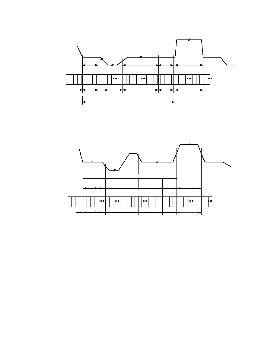
REV. 0
ADV7196A
34
F
F
0
0
INPUT PIXELS
0
0
F
V
H*
F
F
0
0
F
V
H*
0
0
C
b
Y
C
r
Y
C
r
Y
4 CLOCK
853
799
857 0
719
736
723
719
4 CLOCK
DIGITAL HORIZONTAL BLANKING
SAMPLE NUMBER
ANCILLARY DATA
(OPTIONAL)
SAV CODE
EAV CODE
DIGITAL
ACTIVE LINE
ANALOG WAVEFORM
SMPTE293M
0HDATUM
FVH* = FVH AND PARITY BITS
SAV: LINE 43 525 = 200H
SAV: LINE 1 42 = 2AC
EAV: LINE 43 525 = 274H
EAV: LINE 1 42 = 2D8
Figure 65. EAV/SAV Input Data Timing Diagram--SMPTE293M
F
F
0
0
INPUT PIXELS
0
0
F
V
H*
F
F
0
0
F
V
H*
0
0
C
b
Y
C
r
C
r
Y
4 CLOCK
SAMPLE NUMBER
EAV CODE
DIGITAL
ACTIVE LINE
ANALOG WAVEFORM
SMPTE274M
4 CLOCK
2112
2116 2156
2199
440
188
192
2111
4T
SAV CODE
4T
1920T
272T
ANCILLARY DATA (OPTIONAL)
OR BLANKING CODE
DIGITAL HORIZONTAL BLANKING
0HDATUM
FVH* = FVH AND PARITY BITS
SAV/EAV: LINE 1562: F = 0
SAV/EAV: LINE 5631125: F = 1
SAV/EAV: LINE 120; 561583; 11241125: V = 1
SAV/EAV: LINE 21560; 5841123: V = 0
0
Figure 66. EAV/SAV Input Data Timing Diagram--SMPTE274M
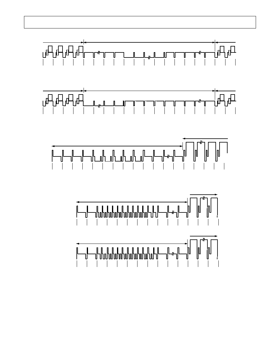
REV. 0
ADV7196A
35
522
523
524
525
1
2
5
6
7
8
9
12
13
10
11
ACTIVE VIDEO
12
42
43
44
ACTIVE VIDEO
VERTICAL BLANK
Figure 67. SMPTE293M (525p)
622
623
624
625
1
2
4
5
6
7
8
9
10
11
12
ACTIVE VIDEO
13
43
44
45
ACTIVE VIDEO
VERTICAL BLANK
Figure 68. ITU-R. BT1358 (625p)
747
748
749
750
1
2
3
4
5
6
7
8
25
26
27
744
745
DISPLAY
VERTICAL BLANKING INTERVAL
Figure 69. SMPTE296M (720p)
1124
1125
1
2
3
4
5
6
7
8
20
21
22
560
DISPLAY
VERTICAL BLANKING INTERVAL
FIELD 1
561
562
563
564
565
566
567
568
569
570
583
584
585
1123
DISPLAY
VERTICAL BLANKING INTERVAL
FIELD 2
Figure 70. SMPT274M (1080i)
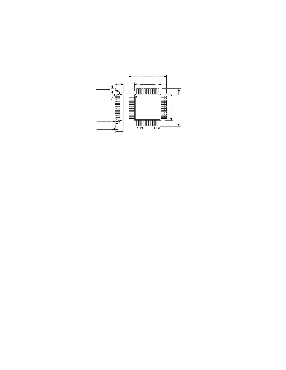
REV. 0
ADV7196A
36
52-Lead Plastic Quad Flatpack (MQFP)
(S-52)
TOP VIEW
(PINS DOWN)
1
13
14
27
26
39
40
52
PIN 1
0.014 (0.35)
0.010 (0.25)
0.557 (14.15)
0.537 (13.65)
0.398 (10.11)
0.390 (9.91)
0.557 (14.15)
0.537 (13.65)
0.398 (10.11)
0.390 (9.91)
0.0256
(0.65)
BSC
0.082 (2.09)
0.078 (1.97)
0.012 (0.30)
0.006 (0.15)
0.008 (0.20)
0.006 (0.15)
SEATING
PLANE
0.037 (0.95)
0.026 (0.65)
0.094 (2.39)
0.084 (2.13)
OUTLINE DIMENSIONS
Dimensions shown in inches and (mm).
C021541.54/01(0)
PRINTED IN U.S.A.
Document Outline
- Specifications
- Pinout
- Package Drawings
- Ordering Guide
- Features
- Applications
- Product Description
- Absolute Maximum Ratings
- Functional Block Diagram
- Pin Function Description
- TABLE OF CONTENTS
- CAUTION
- PROGRAMMABLE SHARPNESS FILTER
- PROGRAMMABLE ADAPTIVE FILTER CONTROL
- MPU PORT DESCRIPTION
- REGISTER ACCESSES
- REGISTER PROGRAMMING
- MODE REGISTER 0 MR0 (MR07-MR00)
- MR0 BIT DESCRIPTION
- MR1 (MR17ÒMR10)
- MR1 BIT DESCRIPTION
- MODE REGISTER 2
- MR1 (MR27-MR20)
- CGMS CRC (MR27)
- MR2 BIT DESCRIPTION
- MODE REGISTER 3
- MR3 (MR37-MR30)
- MR3 BIT DESCRIPTION MR4 BIT DESCRIPTION
- COLOR Y CY (CY7-CY10)
- COLOR CR CCR (CCR7-CCR0)
- COLOR CB CCB (CCB7-CCB0)
- CCB (CCB7-CCB0)
- CGMS DATA REGISTERS 2-0 CGMS2 (CGMS27-CGMS20)
- CGMS1 (CGMS17-CGMS10)
- MODE REGISTER 6
- MR6 (MR67-MR60)
- MR6 BIT DESCRIPTION
- FILTER GAIN FG (FG7-FG0)
- FG BIT DESCRIPTION
- GAMMA CORRECTION REGISTERS 0Ò13
- SHARPNESS FILTER CONTROL AND ADAPTIVE FILTER CONTROL
- SHARPNESS FILTER MODE
- ADAPTIVE FILTER MODE
- ADAPTIVE FILTER GAIN 1
- ADAPTIVE FILTER THRESHOLD A
- ADAPTIVE FILTER GAIN 2
- ADAPTIVE FILTER THRESHOLD B
- ADAPTIVE FILTER GAIN 3
- SHARPNESS FILTER AND ADAPTIVE FILTER APPLICATION EXAMPLES
- HDTV MODE MODE REGISTER 0
- MR0 (MR07-MR00)
- HEXMR0 BIT DESCRIPTION
- MR1 (MR17-MR10)
- MR1 BIT DESCRIPTION
- MODE REGISTER 2
- MR1 (MR27-MR20)
- MR4 (MR47-MR40)
- MR5 BIT DESCRIPTION
- REGISTER SETTINGS
- DIAGRAMS
- 4:4:4 RGB Input Data Format Timing Diagram
- 4:2:2 Input Data Format Timing Diagram
- 4:4:4 YCrCb Input Data Format Timing Diagram
- Input Timing Diagram
- MPU Port Timing Diagram
- Slave Address
- Bus Data Transfer
- Write and Read Sequence
- Subaddress Registers in Progressive Scan Mode
- Subaddress Registers in HDTV Mode
- Mode Register 0
- Async Timing ModeProgramming Input Control Signals for SMPTE295M Compatibility
- DV Input Control Signal in Relation to Video Output Signal
- Mode Register 1
- Y and Color Delay
- Mode Register 2
- Mode Register 3
- Model Register 4
- Mode Register 5
- Color Y Register
- Color Cr Register
- Color Cb Register
- CGMS2 Data Register
- CGMS1 Data Register
- CGMS0 Data Register
- Mode Register 6
- CGMS Waveform
- Filter Gain Register
- Adaptive Filter Gain 3 Register
- Adaptive Filter Gain 1 Register
- Adaptive Filter Threshold A Register
- Adaptive Filter Gain 2 Register
- Adaptive Filter Threshold B Register
- Adaptive Filter Threshold C Register
- Mode Register 0
- Mode Register 1
- Y and Color Delay
- Mode Register 2
- Mode Register 3
- Mode Register 4
- Mode Register 5
- Circuit Layout
- Output Buffer and Optional Filter
- Example for Output Filter: PS Mode/ 2x Oversampling
- EAV/SAV Input Data Timing DiagramSMPTE293M
- EAV/SAV Input Data Timing DiagramSMPTE274M