REV. 0
Information furnished by Analog Devices is believed to be accurate and
reliable. However, no responsibility is assumed by Analog Devices for its
use, nor for any infringements of patents or other rights of third parties
which may result from its use. No license is granted by implication or
otherwise under any patent or patent rights of Analog Devices.
a
ADV7194*
One Technology Way, P.O. Box 9106, Norwood, MA 02062-9106, U.S.A.
Tel: 781/329-4700
World Wide Web Site: http://www.analog.com
Fax: 781/326-8703
© Analog Devices, Inc., 2000
Professional
Extended-10
TM
Video Encoder with 54 MHz Oversampling
SIMPLIFIED BLOCK DIAGRAM
I
2
C INTERFACE
CHROMA
LPF
10-BIT
DAC
10-BIT
DAC
10-BIT
DAC
10-BIT
DAC
10-BIT
DAC
10-BIT
DAC
2
OVERSAMPLING
4
OVERSAMPLING
OR
ADV7194
SSAF
LPF
LUMA
LPF
COMPOSITE VIDEO
Y [S-VIDEO]
C [S-VIDEO]
RGB
YUV
YPrPb
TV SCREEN
OR
PROGRESSIVE
SCAN DISPLAY
COLOR CONTROL
DNR
GAMMA
CORRECTION
VBI
TELETEXT
CLOSED CAPTION
CGMS/WSS
DEMUX
AND
YCrCb-
TO-
YUV
MATRIX
PLL
AND
54MHz
VIDEO
INPUT
PROCESSING
VIDEO
OUTPUT
PROCESSING
VIDEO
SIGNAL
PROCESSING
ANALOG
OUTPUT
27MHz
CLOCK
ITUR.BT
656/601
10-BIT YCrCb
IN 4:2:2 FORMAT
DIGITAL
INPUT
*This device is protected by U.S. Patent Numbers 4631603, 4577216, and 4819098 and other intellectual property rights.
Extended-10 is a trademark of Analog Devices, Inc. This technology combines 10-bit conversion, 10-bit digital video data processing, and 10-bit external interfacing.
SSAF is a trademark of Analog Devices Inc.
ITU-R and CCIR are used interchangeably in this document (ITU-R has replaced CCIR recommendations).
I
2
C is a registered trademark of Philips Corporation.
FEATURES
10-Bit Extended CCIR-656 Input Data Port
Six High-Quality 10-Bit Video DACs
10-Bit Internal Digital Video Processing
Multistandard Video Input
Multistandard Video Output
4 Oversampling with Internal 54 MHz PLL
Programmable Video Control Includes:
Digital Noise Reduction
Gamma Correction
Black Burst
LUMA Delay
CHROMA Delay
Multiple Luma and Chroma Filters
Luma SSAFTM (Super Sub-Alias Filter)
Average Brightness Detection
Field Counter
CGMS (Copy Generation Management System)
WSS (Wide Screen Signaling)
Closed Captioning Support
Teletext Insertion Port (PAL-WST)
2-Wire Serial MPU Interface (I
2
C Compatible and
Fast I
2
C)
Supply Voltage 5 V and 3.3 V Operation
80-Lead LQFP Package
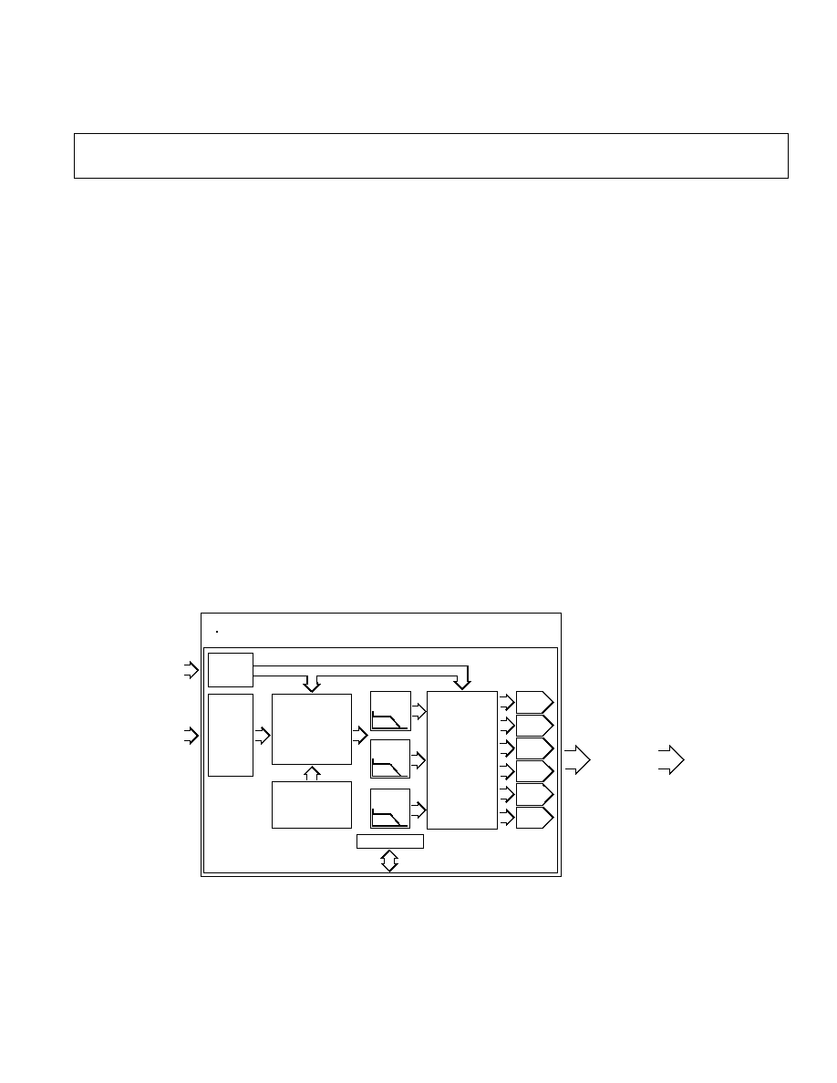
GENERAL DESCRIPTION
The ADV7194 is part of the new generation of video encoders
from Analog Devices. The device builds on the performance of
previous video encoders and provides new features like inter-
facing progressive scan devices, digital noise reduction, gamma
correction, 4
× oversampling and 54 MHz operation, average
brightness detection, black burst signal generation, chroma delay,
an additional Chroma Filter, etc.
The ADV7194 supports NTSC-M, NTSC-N (Japan), PAL N,
PAL-B/D/G/H/I and PAL-60 standards. Input standards sup-
ported include ITU-R.BT656 4:2:2 YCrCb in 8-, 10-, 16- or
20-bit format and 3
× 10-bit YCrCb progressive scan format.
The ADV7194 can output composite video (CVBS), S-Video
(Y/C), Component YUV or RGB and analog progressive scan in
YPrPb format. The analog component output is also compatible
with Betacam, MII and SMPTE/EBU N10 levels, SMPTE 170M
NTSC and ITU-R.BT 470 PAL.
For more information about the ADV7194's features refer to
Detailed Description of Features section.
APPLICATIONS
Professional DVD Playback Systems
PC Video/Multimedia Playback Systems
Progressive Scan Playback Systems
Professional Studio Equipment

ADV7194
2
REV. 0
CONTENTS
FEATURES . . . . . . . . . . . . . . . . . . . . . . . . . . . . . . . . . . . . . 1
APPLICATIONS . . . . . . . . . . . . . . . . . . . . . . . . . . . . . . . . . 1
GENERAL DESCRIPTION . . . . . . . . . . . . . . . . . . . . . . . . . 1
SIMPLIFIED BLOCK DIAGRAM . . . . . . . . . . . . . . . . . . . 1
SPECIFICATIONS
5 V Specifications . . . . . . . . . . . . . . . . . . . . . . . . . . . . . . . . 3
3.3 V Specifications . . . . . . . . . . . . . . . . . . . . . . . . . . . . . . 4
5 V Dynamic Specifications . . . . . . . . . . . . . . . . . . . . . . . . 5
3.3 V Dynamic Specifications . . . . . . . . . . . . . . . . . . . . . . . 5
5 V Timing Characteristics . . . . . . . . . . . . . . . . . . . . . . . . 6
3.3 V Timing Characteristics . . . . . . . . . . . . . . . . . . . . . . . 7
ABSOLUTE MAXIMUM RATINGS . . . . . . . . . . . . . . . . . 9
PIN CONFIGURATION . . . . . . . . . . . . . . . . . . . . . . . . . . . 9
ORDERING GUIDE . . . . . . . . . . . . . . . . . . . . . . . . . . . . . . 9
PACKAGE THERMAL PERFORMANCE . . . . . . . . . . . . . 9
PIN FUNCTION DESCRIPTIONS . . . . . . . . . . . . . . . . . 10
DETAILED DESCRIPTION OF FEATURES . . . . . . . . . 11
GENERAL DESCRIPTION . . . . . . . . . . . . . . . . . . . . . . . . 11
DATA PATH DESCRIPTION . . . . . . . . . . . . . . . . . . . . . 12
INTERNAL FILTER RESPONSE . . . . . . . . . . . . . . . . . . . 13
FEATURES: FUNCTIONAL DESCRIPTION . . . . . . . . . 17
BLACK BURST OUTPUT . . . . . . . . . . . . . . . . . . . . . . . . 17
BRIGHTNESS DETECT . . . . . . . . . . . . . . . . . . . . . . . . . . 17
CHROMA/LUMA DELAY . . . . . . . . . . . . . . . . . . . . . . . . 17
CLAMP OUTPUT . . . . . . . . . . . . . . . . . . . . . . . . . . . . . . . 17
CSO, HSO AND VSO OUTPUTS . . . . . . . . . . . . . . . . . . . 17
COLOR BAR GENERATION . . . . . . . . . . . . . . . . . . . . . . 17
COLOR BURST SIGNAL CONTROL . . . . . . . . . . . . . . . 17
COLOR CONTROLS . . . . . . . . . . . . . . . . . . . . . . . . . . . . 17
CHROMINANCE CONTROL . . . . . . . . . . . . . . . . . . . . . 17
UNDERSHOOT LIMITER . . . . . . . . . . . . . . . . . . . . . . . . 18
DIGITAL NOISE REDUCTION . . . . . . . . . . . . . . . . . . . . 18
DOUBLE BUFFERING . . . . . . . . . . . . . . . . . . . . . . . . . . . 18
GAMMA CORRECTION CONTROL . . . . . . . . . . . . . . . 18
NTSC PEDESTAL CONTROL . . . . . . . . . . . . . . . . . . . . . 18
POWER-ON
RESET . . . . . . . . . . . . . . . . . . . . . . . . . . . . . 18
PROGRESSIVE SCAN INPUT . . . . . . . . . . . . . . . . . . . . . 18
REAL-TIME CONTROL, SUBCARRIER RESET, AND
TIMING RESET . . . . . . . . . . . . . . . . . . . . . . . . . . . . . . . 19
SCH PHASE MODE . . . . . . . . . . . . . . . . . . . . . . . . . . . . . 19
SLEEP MODE . . . . . . . . . . . . . . . . . . . . . . . . . . . . . . . . . . 19
SQUARE PIXEL MODE . . . . . . . . . . . . . . . . . . . . . . . . . . 19
VERTICAL BLANKING DATA INSERTION
AND
BLANK INPUT . . . . . . . . . . . . . . . . . . . . . . . . . . . 19
YUV LEVELS . . . . . . . . . . . . . . . . . . . . . . . . . . . . . . . . . . . 20
20-/16-BIT INTERFACE . . . . . . . . . . . . . . . . . . . . . . . . . . 20
4
× OVERSAMPLING AND INTERNAL PLL . . . . . . . . . 20
VIDEO TIMING DESCRIPTION . . . . . . . . . . . . . . . . . . . 20
RESET SEQUENCE . . . . . . . . . . . . . . . . . . . . . . . . . . . . . 20
MPU PORT DESCRIPTION . . . . . . . . . . . . . . . . . . . . . . . 28
REGISTER ACCESSES . . . . . . . . . . . . . . . . . . . . . . . . . . . 29
REGISTER PROGRAMMING . . . . . . . . . . . . . . . . . . . . . 29
MODE REGISTERS 09 . . . . . . . . . . . . . . . . . . . . . . . 3035
TIMING REGISTERS 017 . . . . . . . . . . . . . . . . . . . . . . . 36
SUBCARRIER FREQUENCY AND
PHASE REGISTERS . . . . . . . . . . . . . . . . . . . . . . . . . . . 37
CLOSED CAPTIONING REGISTERS . . . . . . . . . . . . . . . 37
NTSC PEDESTAL/PAL TELETEXT CONTROL
REGISTERS . . . . . . . . . . . . . . . . . . . . . . . . . . . . . . . . . . 37
TELETEXT REQUEST CONTROL REGISTER . . . . . . 38
CGMS_WSS REGISTERS . . . . . . . . . . . . . . . . . . . . . . . . . 38
CONTRAST CONTROL REGISTERS . . . . . . . . . . . . . . . 39
COLOR CONTROL REGISTERS . . . . . . . . . . . . . . . . . . 39
HUE ADJUST CONTROL REGISTER (HCR) . . . . . . . . 40
HCR BIT DESCRIPTION . . . . . . . . . . . . . . . . . . . . . . . . . 40
BRIGHTNESS CONTROL REGISTER (BCR) . . . . . . . . 40
BCR BIT DESCRIPTION . . . . . . . . . . . . . . . . . . . . . . . . . 40
SHARPNESS RESPONSE REGISTER (PR) . . . . . . . . . . . 41
PR BIT DESCRIPTION . . . . . . . . . . . . . . . . . . . . . . . . . . 41
DNR REGISTERS . . . . . . . . . . . . . . . . . . . . . . . . . . . . . . . 41
DNR BIT DESCRIPTIONS . . . . . . . . . . . . . . . . . . . . . . . . 41
GAMMA CORRECTION REGISTERS . . . . . . . . . . . . . . 43
BRIGHTNESS DETECT REGISTER . . . . . . . . . . . . . . . . 44
OUTPUT CLOCK REGISTER . . . . . . . . . . . . . . . . . . . . . 44
OCR BIT DESCRIPTION . . . . . . . . . . . . . . . . . . . . . . . . . 44
APPENDIX 1
Board Design and Layout Considerations . . . . . . . . . . . . 45
APPENDIX 2
Closed Captioning . . . . . . . . . . . . . . . . . . . . . . . . . . . . . . 47
APPENDIX 3
Copy Generation Management System (CGMS) . . . . . . . 48
APPENDIX 4
Wide Screen Signaling . . . . . . . . . . . . . . . . . . . . . . . . . . . 49
APPENDIX 5
Teletext Insertion . . . . . . . . . . . . . . . . . . . . . . . . . . . . . . . 50
APPENDIX 6
Optional Output Filter . . . . . . . . . . . . . . . . . . . . . . . . . . . 51
APPENDIX 7
DAC Buffering . . . . . . . . . . . . . . . . . . . . . . . . . . . . . . . . . 52
APPENDIX 8
Recommended Register Values . . . . . . . . . . . . . . . . . . . . 53
Power-On Reset Register Values . . . . . . . . . . . . . . . . . . . 55
APPENDIX 9
NTSC Waveforms (With Pedestal) . . . . . . . . . . . . . . . . . 56
NTSC Waveforms (Without Pedestal) . . . . . . . . . . . . . . . 57
PAL Waveforms . . . . . . . . . . . . . . . . . . . . . . . . . . . . . . . . 58
UV Waveforms . . . . . . . . . . . . . . . . . . . . . . . . . . . . . . . . . 60
Output Waveforms . . . . . . . . . . . . . . . . . . . . . . . . . . . . . . 61
Video Measurement Plots . . . . . . . . . . . . . . . . . . . . . . . . 64
APPENDIX 10
Vector Plots . . . . . . . . . . . . . . . . . . . . . . . . . . . . . . . . . . . 68
OUTLINE DIMENSIONS . . . . . . . . . . . . . . . . . . . . . . . . . 69