 | ÐлекÑÑоннÑй компоненÑ: ADT14 | СкаÑаÑÑ:  PDF PDF  ZIP ZIP |
Äîêóìåíòàöèÿ è îïèñàíèÿ www.docs.chipfind.ru
REV. 0
Information furnished by Analog Devices is believed to be accurate and
reliable. However, no responsibility is assumed by Analog Devices for its
use, nor for any infringements of patents or other rights of third parties
which may result from its use. No license is granted by implication or
otherwise under any patent or patent rights of Analog Devices.
a
ADT14
One Technology Way, P.O. Box 9106, Norwood, MA 02062-9106, U.S.A.
Tel: 617/329-4700
World Wide Web Site: http://www.analog.com
Fax: 617/326-8703
© Analog Devices, Inc., 1997
Quad Setpoint, Programmable
Temperature Monitor and Controller
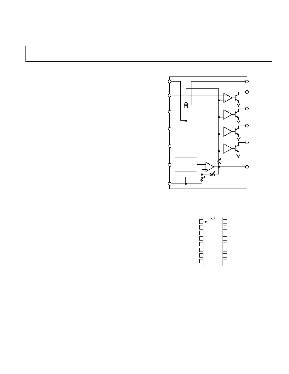
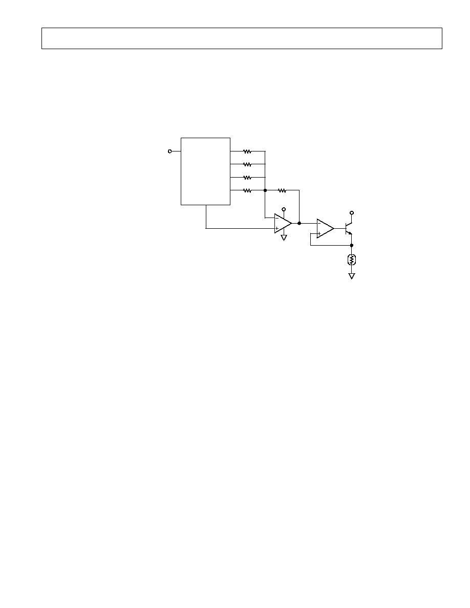
FUNCTIONAL BLOCK DIAGRAM
VOLTAGE
REFERENCE
AND
SENSOR
CURRENT
MIRROR
WINDOW
COMPARATORS
HYSTERESIS
VOLTAGE
TEMPERATURE
OUTPUT
HYSTERESIS
SETPOINT
OUTPUT 1
SETPOINT
OUTPUT 2
SETPOINT
OUTPUT 3
SETPOINT
OUTPUT 4
VPTAT
2.5V
V
REF
SET 1
SET 2
SET 3
SET 4
GND
V+
ADT14
PIN CONFIGURATIONS
DIP & SO
14
13
12
11
16
15
10
9
8
1
2
3
4
7
6
5
TOP VIEW
(Not to Scale)
ADT14
NC = NO CONNECT
OUTPUT 1
V+
2.5V REFERENCE
SETPOINT 4
OUTPUT 4
SETPOINT 1
NC
NC
SETPOINT 3
HYSTERESIS
NC
GROUND
VPTAT
SETPOINT 2
OUTPUT 2
OUTPUT 3
FEATURES
Four Programmable Temperature Setpoints
Programmable Thermal Hysteresis
Accuracy 3 C Typ from 40 C to +125 C
Temperature Output Scale Factor = 5 mV/K
Resistor Programmable Temperature Setpoints
5 mA Open-Collector Setpoint Outputs
Internal 2.5 V Reference
600 A Max Quiescent Current at +5 V
APPLICATIONS
Power Supply Monitor and Control System
Multiple Fan Controller System
Workstation Thermal Management System
GENERAL DESCRIPTION
The ADT14 is a temperature sensor and controller that generates
an output voltage proportional to temperature and provides four
temperature trip points. The four trip points, or temperature
setpoints, and their hysteresis are determined by voltage levels set
by the user. An on-chip voltage reference provides an easy method
for setting the temperature trip points.
The ADT14 consists of a bandgap voltage reference combined
with four matched comparators. The reference provides both a
temperature-stable 2.5 V output, and a voltage proportional to
absolute temperature (VPTAT) which has a precise temperature
coefficient of 5 mV/K = 5 mV/(
°
C +273.15). The VPTAT out-
put is nominally 1.49 V at +25
°
C. The comparators determine
whether the VPTAT output is above the voltages set up by
external resistive dividers (temperature trip points) and generate
an open-collector output signal when one of their respective
thresholds has been exceeded.
Hysteresis is programmed by a user-selected voltage at the hys-
teresis pin. This voltage adjusts the hysteresis current which is
used to generate a hysteresis offset voltage. The comparator's
noninverting inputs are connected in parallel, which guarantees
that there is no hysteresis overlap and eliminates erratic transi-
tions between adjacent trip zones.
Using a proprietary thin-film resistor process in conjunction
with production laser trimming, a temperature accuracy of
±
3
°
C
at 25
°
C is guaranteed. The open-collector outputs are capable
of sinking 5 mA, and provide TTL/CMOS logic compatibility
with an external pull-up resistor. Operating from a single 5 V
supply, the quiescent current is 600
µ
A max.
The ADT14 is available in the 16-lead epoxy DIP and SO
(small outline) packages.

2
REV. 0
ADT14GSPECIFICATIONS
(V+ = 5 V, 40 C
T
A
+125 C unless otherwise noted)
Parameter
Symbol
Conditions
Min
Typ
Max
Units
ACCURACY
Accuracy (Setpoints 1, 2, 3 and 4)
T
A
= +25
°
C
±
2
±
3
°
C
Accuracy (Setpoints 1, 2, 3 and 4)
T
A
= 40
°
C to +125
°
C
±
3
±
5
°
C
VPTAT Output Scale Factor
+4.9
+5
+5.1
mV/K
Setpoint Hysteresis Levels
T
A
= +25
°
C
0.65, 1.5, 5
°
C
Power Supply Rejection Ratio
PSRR
4.5 V
V
S
13 V
0.1
0.25
°
C/V
Linearity
0.5
°
C
SETPOINT INPUTS
Offset Voltage
V
OS
T
A
= +25
°
C
1
mV
Offset Voltage Mismatch
T
A
= +25
°
C
0.5
mV
Output Voltage Drift
TCV
OS
3
µ
V/
°
C
Input Bias Current
I
B
25
100
nA
REFERENCE OUTPUT
Line Regulation
4.5 V
V
S
13 V
±
0.1
%/V
Load Regulation
I
SOURCE
= 10
µ
A to 500
µ
A
±
0.25
%/mA
Output Voltage
V
REF
T
A
= +25
°
C, No Load
2.49
2.5
2.51
V
Output Voltage
V
REF
No Load, 40
°
C
T
A
+125
°
C
2.48
2.5
2.52
V
Output Drift
TCV
REF
±
30
ppm/
°
C
OPEN-COLLECTOR OUTPUTS
Output Low Voltage
V
OL
I
SINK
= 1.6 mA,
40
°
C
T
A
+85
°
C
0.25
0.4
V
Output Low Voltage
V
OL
I
SINK
= 5 mA
0.6
V
Output Leakage Current
I
OH
V+ = 12 V
1
100
µ
A
Fall Time
t
HL
See Figure 1
40
ns
POWER SUPPLY
Supply Range
V+
4.5
5.5
V
Supply Current
I
SY
Unloaded at +5 V
400
600
µ
A
Supply Current
I
SY
Unloaded at +12 V
450
µ
A
Specifications subject to change without notice.
ABSOLUTE MAXIMUM RATINGS*
Maximum Supply Voltage . . . . . . . . . . . . . . 0.3 V to +15 V
Maximum Setpoint Input Voltage . . 0.3 V to ([V+] +0.3 V)
Maximum Reference Output Current . . . . . . . . . . . . . . 1 mA
Maximum Open-Collector Output Current . . . . . . . . . 15 mA
Maximum Open-Collector Output Voltage . . . . . . . . . +15 V
Operating Temperature Range . . . . . . . . . 55
°
C to +150
°
C
Dice Junction Temperature . . . . . . . . . . . . . . . . . . . . +175
°
C
Storage Temperature Range . . . . . . . . . . . 65
°
C to +160
°
C
Lead Temperature (Soldering, 60 sec) . . . . . . . . . . . +300
°
C
*CAUTION
1. Stresses above those listed under Absolute Maximum
Ratings may cause permanent damage to the device. This is
a stress rating only; functional operation at or above this
specification is not implied. Exposure to the above maximum
rating conditions for extended periods may affect device
reliability.
2. Digital inputs are protected; however, permanent damage
may occur on unprotected units from high-energy electro-
static fields. Keep units in conductive foam or packaging at all
times until ready to use. Use proper antistatic handling
procedures.
3. Remove power before inserting or removing units from their
sockets.
ORDERING GUIDE
Temperature
Package
Package
Model/Grade
Range
1
Description
Options
2
ADT14GP
XIND
Plastic DIP
N-16
ADT14GS
XIND
SOIC
R-16A
NOTES
1
XIND = 40 C to 125 C.
2
N = Plastic DIP; R = Small Outline.
THERMAL PACKAGE CHARACTERISTICS
Package Type
JA
JC
Units
16-Lead Plastic DIP
103
34
C/W
16-Lead SOIC
81
27
C/W
V+
1k
20pF
Figure 1. Test Load
ADT14
3
REV. 0
WAFER TEST LIMITS
Parameter
Symbol
Conditions
Min
Typ
Max
Units
INPUTS SET HIGH, SET LOW
Input Bias Current
I
B
70
nA
OUTPUT VPTAT
Temperature Accuracy
T
A
= +25
°
C, No Load
1.5
°
C
OUTPUT V
REF
Nominal Value
V
REF
T
A
= +25
°
C, No Load
2.490
2.510
V
Line Regulation
4.5 V
V
13.2 V
±
0.08
%/V
Load Regulation
10
µ
A
IV
REF
500
µ
A
±
0.25
%/mA
OPEN-COLLECTOR OUTPUTS OVER, UNDER
Output Low Voltage
V
OL
I
SINK
= 1.6 mA
0.4
V
Output Leakage Current
I
OH
100
µ
A
POWER SUPPLY
Supply Range
V+
4.5
5.5
V
Supply Current
I
SY
Unloaded
600
µ
A
NOTE
Electrical tests are performed at wafer probe to the limits shown. Due to variations in assembly and nominal yield loss, yield after packaging is not guaranteed for
standard product dice. Consult factory to negotiate specifications based on lot qualification through sample lot assembly and testing.
DICE CHARACTERISTICS
Die Size 0.069
×
0.080 inch, 5520 sq. mils
(1.75
×
2.03 mm, 3.55 sq. mm)
Transistor Count: 130
(V+ = +5 V, GND = 0 V, T
A
= +25 C unless otherwise noted)
WARNING!
ESD SENSITIVE DEVICE
CAUTION
ESD (electrostatic discharge) sensitive device. Electrostatic charges as high as 4000 V readily
accumulate on the human body and test equipment and can discharge without detection.
Although the ADT14 features proprietary ESD protection circuitry, permanent damage may
occur on devices subjected to high energy electrostatic discharges. Therefore, proper ESD
precautions are recommended to avoid performance degradation or loss of functionality.
ADT14
4
REV. 0
Typical Performance Characteristics
AIR VELOCITY FPM
0
0
700
100
200
300
400
500
600
160
100
80
40
20
140
120
60
TIME CONSTANT sec
TRANSITION FROM +100
°
C STIRRED OIL BATH
TO FORCED +25
°
C AIR
V+ = +5V, NO LOAD
SOIC SOLDERED TO 0.6" 0.5" Cu PCB
PDIP IN SOLDERTAIL SOCKET
SOLDERED TO 0.8" 0.6" Cu PCB
Figure 2. Thermal Time Constant in Forced Air
TIME sec
100
80
0
0
30
5
10
15
20
25
60
40
20
90
70
50
30
10
CHANGE IN TEMPERATURE %
V+ = +5V, NO LOAD
SOIC SOLDERED TO 0.6" 0.5" Cu PCB
PDIP IN SOLDERTAIL SOCKET
SOLDERED TO 0.8" 0.6" Cu PCB
Figure 3. Thermal Response in Stirred Oil Bath
TEMPERATURE C
5.0
4.5
3.0
75
175
25
25
75
125
4.0
3.5
START-UP VOLTAGE DEFINED AS OUTPUT VALUE
BEING WITHIN 5 C OF OUTPUT AT +5V
NO LOAD
START-UP VOLTAGE V
Figure 4. Start-Up Voltage vs. Temperature
10
0%
40µs
500mV
100
90
5V
0V
1.5V
0V
V
IN
VPTAT
Figure 5. Start-Up Response
5
3
5
50
150
25
25
50
75
125
1
1
3
4
2
0
2
4
100
0
MAX LIMIT
MIN LIMIT
ACCURACY ERROR
°
C
V+ = +5V, NO LOAD
TEMPERATURE
°
C
Figure 6. Accuracy Error vs. Temperature, Stirred Oil Bath
SUPPLY VOLTAGE V
600
0
0
16
2
4
6
8
10
12
14
500
400
300
200
100
T
A
= +25
°
C, NO LOAD
SUPPLY CURRENT
A
Figure 7. Supply Current vs. Supply Voltage
ADT14
5
REV. 0
500
400
300
75
175
25
25
75
125
475
450
350
325
425
375
V+ = +5V, NO LOAD
SUPPLY CURRENT µA
TEMPERATURE
°
C
Figure 8. Supply Current vs. Temperature
40
20
0
75
175
25
25
75
125
35
30
10
5
25
15
V
OL
= +1V, V+ = +5V
OPEN-COLLECTOR SINK CURRENT mA
TEMPERATURE
°
C
Figure 9. Open-Collector Output Sink Current vs.
Temperature
OPEN-COLLECTOR OUTPUT VOLTAGE mV
700
0
75
175
25
25
75
125
600
500
400
300
200
100
I
LOAD
= 1mA
I
LOAD
= 5mA
V+ = +5V, NO LOAD
TEMPERATURE
°
C
Figure 10. Open-Collector Output Voltage vs. Temperature
2.52
2.5
2.48
75
175
25
25
75
125
2.515
2.51
2.49
2.485
2.505
2.495
V+ = +5V, NO LOAD
MAX LIMIT
REFERENCE VOLTAGE V
MIN LIMIT
TEMPERATURE
°
C
Figure 11. Reference Voltage vs. Temperature
TEMPERATURE
°
C
0.1
0
150
25
POWER SUPPLY REJECTION
C/V
0
25
50
75
100
125
0.05
0.025
0.075
50
V+ = +4.5V TO +13V
NO LOAD
Figure 12. VPTAT Power Supply Rejection vs. Temperature
10
0%
500µs
20mV
100
90
2.5V
V
LOAD
0V
V
REF
Figure 13. V
REF
Under Load Switching (0
µ
A500
µ
A),
R
LOAD
= 5 k
ADT14
6
REV. 0
APPLICATIONS INFORMATION
Programming the ADT14
To program any of the four temperature trip points, simply set
the voltage at the setpoint pin equal to the voltage expected at
the VPTAT output at the desired trip temperature. The on-
board 2.5 V precision reference provides a temperature stable
output that is used to establish the setpoint voltages. Figure 14
illustrates the basic temperature setpoint configuration. This
parallel resistor ladder configuration uses six resistors to set the
four setpoint voltages.
I
L
I
L2
R4
I
L1
R1
R2
R5
R3
R6
V
REF
SET 4
SET 3
SET 2
SET 1
GND
ADT14
HYS
Figure 14. ADT14 Setpoint Programming
For SET4,
T4 = 100
°
C
V(SET4) = (T4 + 273.15)(5 mV/K)
For SET1,
T1 = 75
°
C
V(SET1) = (T1 + 273.15)(5 mV/K)
Choose I
L1
= I
L2
= 25
µ
A,
R1 = (V
REF
V[SET4])/I
L1
R2 = (V[SET4] V[SET1])/I
L1
R3 = V(SET1)/I
L1
For SET3,
T3 = 50
°
C
V(SET3) = (T3 + 273.15)(5 mV/K)
For SET2,
T2 = 10
°
C
V(SET2) = (T2 + 273.15)(5 mV/K)
Since I
L1
= I
L2
= 25
µ
A,
R4 = (V
REF
V[SET3])/I
L2
R5 = (V[SET3] V[SET2])/I
L2
R6 = V(SET2)/I
L2
For the example shown in Figure 14 and the related equations,
Setpoint 4 was chosen as highest temperature trip point, fol-
lowed in order by Setpoint 1, Setpoint 3 and Setpoint 2. The
user may choose to alter this order at will as all the setpoint
inputs and trip point outputs are identical in operation. The
minimum recommended parallel ladder resistance is 12.5 k
.
This maintains a V
REF
load current less than 200
µ
A. To avoid
errors, choose 50
µ
A < I
L
< 200
µ
A.
For those applications where setpoints do not need to be
changed, a single ladder of five resistors can be used. Figure 15
illustrates a single resistor ladder configuration.
50
µ
A < I
L
< 200
µ
A
R1 = (V
REF
V[SET4])/I
L
R2 = (V[SET4] V[SET1])/I
L
R3 = (V[SET1] V[SET3])/I
L
R4 = (V[SET3] V[SET2])/I
L
R5 = V(SET2)/I
L
I
L
R1
R2
R3
V
REF
R4
R5
SET4
SET1
SET3
SET2
50 A < I
L
< 200 A
T4 > T1 > T3 > T2
Figure 15. Single Resistor Ladder
Temperature Hysteresis
Temperature hysteresis is the number of degrees below the
original setpoint temperature that must be sensed by the
ADT14 before the setpoint comparator will be reset and the
open-collector output disabled. Figure 16 shows the hysteresis
profile. Hysteresis is programmed by the user by setting a speci-
fied voltage at the hysteresis pin (See Table I).
HYSTERESIS
HI
LO
T
SET2
T
SET3
T
SET1
T
SET4
TEMPERATURE
OUTPUT VOLTAGE
Figure 16. ADT14 Hysteresis Profile
Table I. Common Hysteresis Values and Voltages
Hysteresis
Connect Pin 11 to
0.65
°
C
+2.5 V Reference
1.5
°
C
Leave Open
5
°
C
Ground
The voltage on Pin 11 programs the internal hysteresis current,
which is mirrored and fed to a buffer controlled by an analog
switch. After a temperature setpoint has been exceeded and a
comparator tripped, the buffer is enabled, allowing hysteresis
current to flow. This current generates a hysteresis offset voltage
ADT14
7
REV. 0
across an internal 1 k
resistor at the comparator input. The
comparator output remains on until the voltage at the compara-
tor input, now equal to VPTAT plus the hysteresis offset, has
returned to the setpoint voltage. At this point the comparator
turns off, the open-collector output is deactivated, and the hys-
teresis current buffer is disabled.
While Table I shows simple pin-programmable hysteresis val-
ues, the user may design for intermediate values of hysteresis
between 0.65
°
C and 5
°
C using a resistive divider. To set the
hysteresis in the range 0.65
°
C < T
HYS
< 1.5
°
C, a resistor is
connected from the HYS pin (Pin 11) to V
REF
(Pin 14). The
value of the resistor is given by the following equation:
R1
=
57.5
1.5
-
Hysteresis
57.5
For various values of T
HYS
, the table below shows the values for
R1:
Table II
T
HYS
( C)
R1 (k )
0.7
14.4
0.8
24.6
0.9
38.3
1.0
57.5
1.1
86.3
1.2
134.2
1.3
230
1.4
517.5
To set hysteresis in the range of 1.5
°
C < T
HYS
< 5
°
C, a resistor
is connected from the HYS pin (Pin 11) to the ADT14's com-
mon (Pin 5). The value of the resistor is given by:
R2
=
201.1
Hysteresis 1.5
57.5
For various values of T
HYS
, the table below shows values for R2:
Table III
T
HYS
( C)
R2 (k )
1.6
1953
1.75
746.9
2.0
344.7
2.25
210.6
2.5
143.6
2.75
103.4
3.0
76.6
3.25
57.4
3.50
43.1
3.75
31.8
4.0
22.9
4.25
15.6
4.5
9.5
4.75
4.4
The schematics for the two circuits are shown below. As the
resistor values are approximate, it is a good idea to add a poten-
tiometer for fine adjustments.
V
REF
HYS
ADT14
0.65
°
C < T
HYS
< 1.5
°
C
HYS
ADT14
1.5
°
C < T
HYS
< 5
°
C
R2
P2
R1
P1
Figure 17. Hysteresis Connections for Miscellaneous
Values
Understanding Error Sources
The accuracy of the VPTAT sensor output is well characterized
and specified, however preserving this accuracy in a heating or
cooling control system requires some attention to minimizing
potential error sources. The internal sources of setpoint pro-
gramming error include the initial tolerances and temperature
drifts of the reference voltage V
REF
, the setpoint comparator
input offset voltage and bias current, and the hysteresis current
scale factor. When evaluating setpoint programming errors,
remember that any V
REF
error contribution at the comparator
inputs is reduced by the resistor divider ratios. Each comparator's
input bias current drops to less than 1 nA (typ) when the com-
parator is tripped. This change accounts for some setpoint volt-
age error, equal to the change in bias current multiplied by the
effective setpoint divider ladder resistance to ground.
The thermal mass of the ADT14 package and the degree of
thermal coupling to the surrounding circuitry are the largest
factors in determining the rate of thermal settling, which ulti-
mately determines the rate at which the desired temperature
measurement accuracy may be reached (see Figure 2). Thus,
one must allow sufficient time for the device to reach the final
temperature. The typical thermal time constant for the plastic
SOIC package is approximately 70 seconds in still air. There-
fore, to reach the final temperature accuracy within 1%, a set-
tling time of five time constants, or six minutes, is necessary.
External error sources to consider are the accuracy of the exter-
nal programming resistors, ground voltage errors, and thermal
gradients. The accuracy of the external programming resistors
directly impacts the resulting setpoint accuracy. Thus, in fixed-
temperature applications the user should select resistor toler-
ances appropriate to the desired programming accuracy. Resistor
temperature drift must also be taken into account. This effect
can be minimized by selecting high quality components, and by
keeping all components in close thermal proximity. Applications
requiring high measurement accuracy require great attention to
detail regarding thermal gradients. Careful circuit board layout,
component placement, and protection from stray air currents
are necessary to minimize common thermal error sources. The
user should also take care to keep the bottom of the setpoint
programming divider ladder as close as possible to GND (Pin 5)
to minimize errors due to IR voltage drops and coupling of
external noise sources. In any case, a 0.1
µ
F capacitor for power
supply bypassing is always recommended at the chip.

ADT14
8
REV. 0
Safety Considerations
In heating and cooling system design, designers should antici-
pate potential system fault conditions which may result in sig-
nificant safety hazards which are outside the control of, and
cannot be corrected by, the ADT14 based circuit. Governmen-
tal and industrial regulations regarding safety requirements and
standards for such designs should be observed where applicable.
Self-Heating Effects
In some applications the user should consider the effects of self-
heating due to the power dissipated by the open-collector out-
puts, which are capable of sinking 5 mA each continuously.
Under full load, the ADT14 open-collector output device is
dissipating,
P
DISS
=
0.6V
×
0.005 A
×
4
=
12 mW
which, in the small outline package, accounts for a temperature
increase due to self-heating of
T
=
P
DISS
×
JA
=
0.012 W
×
81
°
C
W
=
0.97
°
C
This will directly affect the accuracy of the ADT14 and will, for
example, cause the device to switch the heating output off 0.97
degrees early. Alternatively, bonding the same package to a
moderate heatsink limits the self-heating effect to approximately
T
=
P
DISS
×
JC
=
0.012 W
×
27
°
C
W
=
0.32
°
C
which is a much more tolerable error in most systems. The V
REF
and VPTAT outputs are also capable of delivering sufficient
current to contribute heating effects and should not be ignored.
Buffering the Voltage Reference
The reference output V
REF
is used to generate the temperature
setpoint programming voltages for the ADT14. The onboard
V
REF
output buffer is capable of 500
µ
A output drive into as
much as a 50 pF load. Exceeding this load will affect the accu-
racy of the reference voltage, will increase thermal errors due to
internal heat generation, and may induce oscillations. External
buffering of V
REF
with a low drift voltage follower will ensure
optimal reference accuracy if a large load current is required.
Amplifiers that offer low drift, low power consumption, and low
cost appropriate to this application include the OP295 and
members of the OP90, OP97, OP177 families, and others shown
in the following applications circuits.
With excellent drift and noise characteristics, V
REF
offers a good
voltage reference for data acquisition and transducer excitation
applications as well.
Preserving Accuracy Over Wide Temperature Range Operation
The ADT14 is unique in offering both a wide-range tempera-
ture sensor and the associated detection circuitry needed to
implement a complete thermostatic control function in one
monolithic device. The voltage reference, setpoint comparators,
and output buffer amplifiers have been carefully compensated to
maintain accuracy over the specified temperature ranges in this
application. Since the ADT14 is both sensor and control circuit,
in many applications the external components used to program
and interface the device are subjected to the same temperature
extremes. Thus, it is necessary to place components in close
thermal proximity to minimize temperature differentials, and to
account for thermal drift errors where appropriate, such as
resistor matching temperature coefficients, amplifier error drift,
and the like. Circuit design with the ADT14 requires a slightly
different perspective regarding the thermal behavior of elec-
tronic components.
Thermal Response Time
The time required for a temperature sensor to settle to a speci-
fied accuracy is a function of the thermal mass of the sensor,
and the thermal conductivity between the sensor and the object
being sensed. Thermal mass is often considered equivalent to
capacitance. Thermal resistance is commonly specified in units
of degrees per watt of power transferred across the thermal joint.
Figure 3 illustrates the typical response to a step change in am-
bient temperature for PDIP and SOIC packages. Thus, the time
required for the ADT14 to settle to the desired accuracy is
dependent on the package selected, the thermal contact estab-
lished in the particular application, and the equivalent thermal
conductivity of the heat source. For most applications, the set-
tling time is probably best determined empirically.
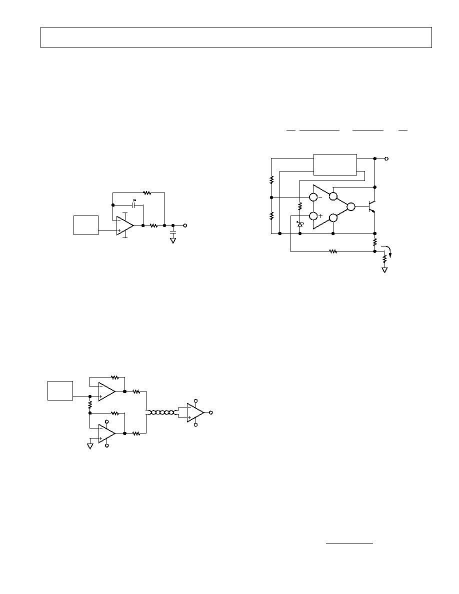
Switching Loads with the Open-Collector Outputs
In many temperature sensing and control applications some type
of switching is required. Whether it's to turn on a heater when
the temperature goes below a minimum value or to turn off a
motor that is overheating, the open-collector outputs can be
used. For the majority of applications, the switches used need to
handle large currents on the order of 1 amp and above. Because
the ADT14 is accurately measuring temperature, the open-
collector outputs should handle less than 5 mA of current to
minimize self-heating. Clearly, the trip point outputs should not
drive the equipment directly. Instead, an external switching
device is required to handle the large currents. Some examples
of these are power MOSFETs, thyristors, IGBTs, and Darlingtons.
Figures 18a18d show a variety of circuits where the ADT14
controls a switch. The main consideration in these circuits is the
current required to activate the switch.
Power FETs are popular for handling a variety of high current
DC loads. Figure 18b shows the ADT14 driving a P-channel
MOSFET transistor for a simple heater circuit. When the out-
put transistor turns on, the gate of the MOSFET is pulled down
to approximately 0.6 V, turning it on. For most MOSFETs a
gate-to-source voltage, or V
GS
, on the order of 2 V to 5 V is
sufficient to turn on the device.
Isolated Gate Bipolar Transistors (IGBT) combine many of the
benefits of power MOSFETs with bipolar transistors, and are
used for a variety of high power applications. Because IGBTs
have a gate similar to MOSFETs, turning the devices on and off
is relatively simple as shown in Figure 18c. The turn-on voltage
for the IGBT shown (IRGB40S) is between 3.0 and 5.5 volts.
This part has a continuous collector current rating of 50 A and a
maximum collector-to-emitter voltage of 600 V, enabling it to
work in very demanding applications.
The last class of high power devices discussed here are thyris-
tors, which include SCRs and triacs. Triacs are a useful alter-
native to relays for switching ac line voltages. The 2N6073A
shown in Figure 18d is rated to handle 4 A (rms). The opto-
isolated MOC3021 triac shown features excellent electrical
isolation from the noisy AC line and complete control over the
high power triac with only a few additional components.
ADT14
9
REV. 0
TEMP
SENSOR
& VOLTAGE
REFERENCE
HYSTERESIS
GENERATOR
13
14
15
9
10
11
12
16
6
7
8
1
2
3
4
5
NC
NC
2604-12-311 COTO
12V
V
REF
MOTOR
SHUTDOWN
IN4001 OR EQUIVALENT
NC = NO CONNECT
ADT14
Figure 18a. Reed Relay Drive
TEMP
SENSOR
& VOLTAGE
REFERENCE
HYSTERESIS
GENERATOR
13
14
15
9
10
11
12
16
6
7
8
1
2
3
4
5
NC
NC
V
REF
IRFR9022 OR
EQUIVALENT
2.4k
(24V)
1.2k
(6V)
5%
IN
OUT
A7812
(24V ONLY)
HEATING
ELEMENT
24V/6V
NC = NO CONNECT
ADT14
Figure 18b. Driving a P-Channel MOSFET
TEMP
SENSOR
& VOLTAGE
REFERENCE
HYSTERESIS
GENERATOR
13
14
15
9
10
11
12
16
6
7
8
1
2
3
4
5
NC
NC
V
REF
4.7k
MOTION
CONTROL
V+
4.7k
1RGBC40S
2N1711
NC = NO CONNECT
ADT14
Figure 18c. Driving an IGBT
TEMP
SENSOR
& VOLTAGE
REFERENCE
HYSTERESIS
GENERATOR
13
14
15
9
10
11
12
16
6
7
8
1
2
3
4
5
NC
NC
V
REF
V+ = +5V
500
MOC3011
1
2
3
6
5
4
150
LOAD
AC
2N6073A
NC = NO CONNECT
ADT14
Figure 18d. Controlling the 2N6073A Triac
ADT14
10
REV. 0
TEMP
SENSOR
& VOLTAGE
REFERENCE
HYSTERESIS
GENERATOR
13
14
15
9
10
11
12
16
6
7
8
1
2
3
4
5
NC
NC
V
REF
V+
4.7k
I
L
Q1
NC = NO CONNECT
ADT14
Figure 19a. An External Resistor Minimizes Self-Heating
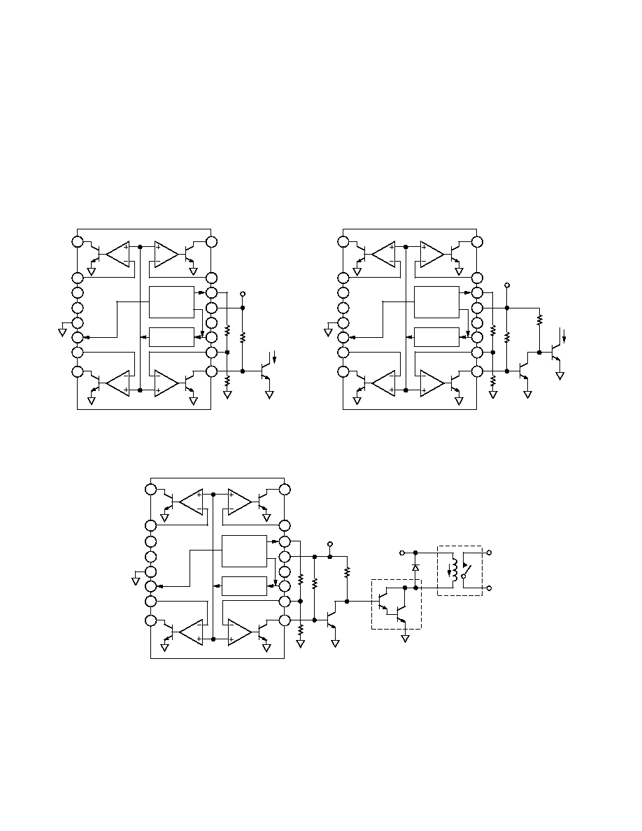
High Current Switching
As mentioned earlier, internal dissipation due to large loads on
the ADT14 outputs will cause some temperature error due to
self-heating. External transistors buffer the load from the ADT14,
so that virtually no power is dissipated in the internal transistors
and minimal self-heating occurs. Figures 19a19c show a few
examples using external transistors. The simplest case uses a
single transistor on the output to invert the output signal as
shown in Figure 19a. When the open-collector of the ADT14
turns ON and pulls the output down, the external transistor Q1's
base will be pulled low, turning off the transistor. Another transis-
tor can be added to reinvert the signal as shown in Figure 19b.
Now, when the output of the ADT14 is pulled down, the first
transistor, Q1, turns off and its collector goes high, which turns
on Q2, pulling its collector low. Thus, the output taken from the
collector of Q2 is identical to the output of the ADT14. By pick-
ing a transistor that can accommodate large amounts of current,
many high power devices can be switched.
An example of a higher power transistor is a standard Darlington
configuration as shown in Figure 19c. The part chosen, TIP-110,
can handle 2 A continuous, which is more than enough to control
many high power relays. In fact the Darlington itself can be used
as the switch, similar to MOSFETs and IGBTs.
TEMP
SENSOR
& VOLTAGE
REFERENCE
HYSTERESIS
GENERATOR
13
14
15
9
10
11
12
16
6
7
8
1
2
3
4
5
NC
NC
V
REF
V+
4.7k
I
L
Q2
2N1711
4.7k
Q1
2N1711
NC = NO CONNECT
ADT14
Figure 19b. Second Transistor Maintains Polarity of
ADT14 Output
TEMP
SENSOR
& VOLTAGE
REFERENCE
HYSTERESIS
GENERATOR
13
14
15
9
10
11
12
16
6
7
8
1
2
3
4
5
NC
NC
V
REF
V+
4.7k
I
L
2N1711
4.7k
TIP110
RELAY
+12V
NC = NO CONNECT
ADT14
Figure 19c. Darlington Transistor Can Handle Large Currents
ADT14
11
REV. 0
Buffering the Temperature Output Pin
The VPTAT sensor output is a low impedance dc output volt-
age with a 5 mV/K temperature coefficient, and is useful in a
number of measurement and control applications. In many
applications, this voltage may need to be transmitted to a central
location for processing. The unbuffered VPTAT voltage output
is capable of 500
µ
A drive into 50 pF (max). As mentioned in
the discussion regarding buffering circuits for the V
REF
output, it
is useful to consider external amplifiers for interfacing VPTAT
to external circuitry to ensure accuracy, and to minimize load-
ing, which could create dissipation-induced temperature sensing
errors. An excellent general-purpose buffer circuit using the
OP177, which is capable of driving over 10 mA and will remain
stable under capacitive loads of up to 0.1
µ
F, is shown in Figure
20. Other interface circuits are shown below.
V+
V
0.1 F
10k
100
V
OUT
OP177
ADT14
VPTAT
Figure 20. Buffer VPTAT to Handle Difficult Loads
Differential Transmitter
In noisy industrial environments, it is difficult to send an accu-
rate analog signal over a significant distance. However, by send-
ing the signal differentially on a wire pair, these errors can be
significantly reduced. Since the noise will be picked up equally
on both wires, a receiver with high common-mode input rejec-
tion can be used very effectively to cancel out the noise at the
receiving end. Figure 21 shows two amplifiers being used to
send the signal differentially, and an excellent differential re-
ceiver, the AMP03, (SSM2141 or SSM2143 are two other
options), which features a common-mode rejection ratio of
95 dB at dc and very low input and drift errors.
V+
V
50
1/2 OP297
ADT14
VPTAT
10k
4.9k
10k
1/2 OP297
50
V+
V
V
OUT
AMP03 OR
SSM2143
Figure 21. Send the Signal Differentially for Noise
Immunity
4 mA to 20 mA Current Loop
Another very common method of transmitting a signal over long
distances is to use a 4 mA-to-20 mA loop (see Figure 22). An
advantage of using a 4 mA-to-20 mA loop is that the accuracy of
a current loop is not compromised by voltage drops across the
line. One requirement of 4 mA-to-20 mA circuits is that the
remote end must receive all of its power from the loop, meaning
that the circuit must consume less than 4 mA. Operating from
+5 V, the quiescent current of the ADT14 is 600
µ
A max, and
the OP90s is 20
µ
A max, totaling much less than 4 mA. Although
not shown, the open collector outputs and temperature setting
pins can be connected to do any local control of switching.
The current is proportional to the voltage on the VPTAT out-
put, and is calibrated to 4 mA at a temperature of 40
°
C, to
20 mA for +85
°
C. The main equation governing the operation
of this circuit gives the current as a function of VPTAT:
I
OUT
=
1
R6
VPTAT
×
R5
R2
-
V
REF
×
R3
R3
+
R1
×
1
+
R5
R2
ADT14
VPTAT
6
7
2
3
4
V+
GND
V
REF
OP90
R2
39.2k
R1
243k
R3
100k
R6
100
R5
100k
2N1711
14
5
13
6
+5V TO +13.2V
R
L
4-20mA
Figure 22. 4 mA to 20 mA Current Loop
To determine the resistor values in this circuit, first note that
V
REF
remains constant over temperature. Thus the ratio of R5
over R2 must give a variation of I
OUT
from 4 mA to 20 mA as
VPTAT varies from 1.165 V at 40
°
C to 1.79 V at +85
°
C. The
absolute value of the resistors is not important, only the ratio.
For convenience, 100 k
is chosen for R5. Once R2 is calcu-
lated, the value of R3 and R1 is determined by substituting
4 mA for I
OUT
and 1.165 V for VPTAT and solving. The final
values are shown in the circuit. The OP90 is chosen for this
circuit because of its ability to operate on a single supply and its
high accuracy. For initial accuracy, a 10 k
trim potentiometer
can be included in series with R3, and the value of R3 lowered
to 95 k
. The potentiometer should be adjusted to produce an
output current of 12.3 mA at 25
°
C.
Temperature-to-Frequency Converter
Another common method of transmitting analog information is
to convert a voltage to the frequency domain. This is easily done
with any of the available low cost monolithic Voltage-to-Fre-
quency Converters (VFCs) that feature an open-collector digital
output. A digital signal is immune to noise and voltage drops
because the only important information is the frequency. As
long as the conversions between temperature and frequency are
accurately performed, the temperature data can be accurately
transmitted.
A simple circuit to do this combines the ADT14 with an AD654
VFC and is shown in Figure 23. The AD654 outputs a square
wave that is proportional to the dc input voltage according to
the following equation:
F
OUT
=
V
IN
10 (R1
+
R2) C
T
ADT14
12
REV. 0
By connecting the VPTAT output to the input of the AD654,
the 5 mV/K, temperature coefficient gives a sensitivity of
25 Hz/
°
C, centered around 7.5 kHz at 25
°
C. The trimming
resistor, R2, is needed to calibrate the absolute accuracy of the
AD654. For more information on the converter, consult the
AD654 data sheet. An AD650 frequency-to-voltage converter
can be used to accurately convert the frequency back to a dc
voltage on the receiving end.
OSC
AD654
8
6
7
1
4
3
5
2
V+
C1
0.1 F
5k
V+
F
OUT
R1
1.8k
R2
500
ADT14
VPTAT
Figure 23. Temperature-to-Frequency Converter
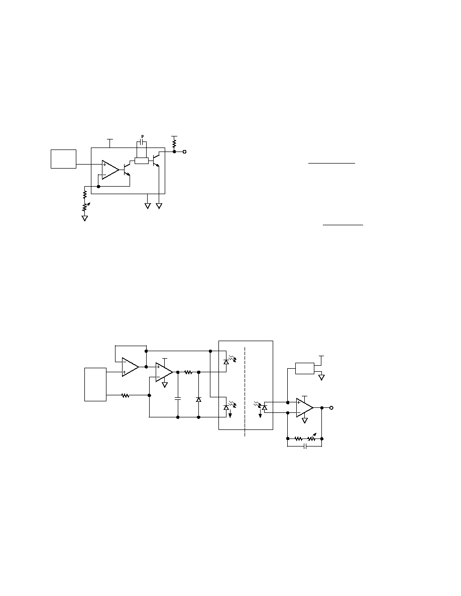
Isolation Amplifier
In many industrial applications the sensor is located in an envi-
ronment that needs to be electrically isolated from the central
processing area. Figure 24 shows a simple circuit that uses an
8-pin opto-isolator (IL300XC) that can operate across a 5,000
V barrier. IC1 (an OP290 single-supply amplifier) is used to
drive the LED connected between Pins 1 to 2. The feedback
actually comes from the photodiode connected to Pins 3 to 4.
The OP290 drives the LED such that there is enough current
generated in the photodiode to exactly equal the current derived
from the VPTAT voltage across the 470 k
resistor. On the
receiving end, an OP90 converts the current from the second
photodiode to a voltage through its feedback resistor R2. Note
that the other amplifier in the dual OP290 is used to buffer the
2.5 V reference voltage of the ADT14 for an accurate, low drift
LED bias level without affecting the programmed hysteresis
current. A REF43 (a precision 2.5 V reference) provides an
accurate bias level at the receiving end.
To understand this circuit, it helps to examine the overall equa-
tion for the output voltage. First, the current (I1) in the photo-
diode is set by:
I1
=
2.5V VPTAT
470 k
Note that the IL300XC has a gain of 0.73 (typical) with a min
and max of 0.693 and 0.769 respectively. Since this is less than
1.0, R2 must be larger than R1 to achieve overall unity gain. To
show this the full equation is:
V
OUT
=
2.5V I 2R2
=
2.5V 0.7
2.5V VPTAT
470 k
×
644 k
=
VPTAT
A trim is included for R2 to correct for the initial gain accuracy
of the IL300XC. To perform this trim, simply adjust for an
output equal to VPTAT at any particular temperature. For
example, at room temperature, VPTAT = 1.49 V, so adjust R2
until V
OUT
= 1.49 V as well. Both the REF43 and the OP90
operate from a single supply, and contribute no significant error
due to drift.
In order to avoid the accuracy trim, and to reduce board space,
complete isolation amplifiers, such as the high accuracy AD202,
are available.
OP290
OP290
V+
ADT14
V
REF
VPTAT
60µF
100
IN9148
I
1
I
2
IL300XC
1
2
3
4
OP90
ISOLATION
BARRIER
V+
2.5V
6
2
4
V+
604k
100k
680pF
1.16V TO 1.7V
R1
470k
REF43
Figure 24. Isolation Amplifier
ADT14
13
REV. 0
Out-of-Range Warning
In Figure 25, connecting an open-collector output of the
ADT14 and an inverted open-collector output together into a
wired-OR configuration, a temperature "out-of-range" warning
signal is generated. This can be useful in sensitive equipment
calibrated to work over a limited temperature range.
TEMP
SENSOR
& VOLTAGE
REFERENCE
HYSTERESIS
GENERATOR
13
14
15
9
10
11
12
16
6
7
8
1
2
3
4
5
NC
NC
V
REF
47k
200
LED
V+
NC
NC = NO CONNECT
ADT14
2N1711
Figure 25. Out-of-Range Warning
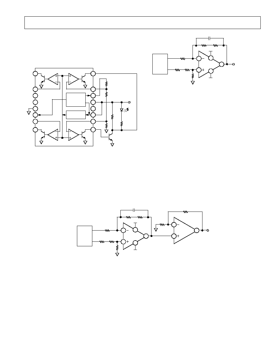
Translating 5 mV/K to 10 mV/ C
A useful circuit is shown in Figure 26 that translates the
VPTAT output voltage, which is calibrated in Kelvins, into an
output that can be read directly in degrees Celsius on a voltme-
ter display. To accomplish this, an external amplifier is config-
ured as a differential amplifier. The resistors are scaled so the
V
REF
voltage will exactly cancel the VPTAT voltage at 0.0
°
C.
6
7
2
3
4
OP177
+15V
105k
4.22k
10pF
15V
100k
100k
4.12k
487
V
OUT
(10mV/
°
C)
(V
OUT
= 0.0V
@ T = 0.0
°
C)
ADT14
V
REF
VPTAT
14
6
Figure 26. Translating 5 mV/K to 10 mV/ C
However, the gain from VPTAT to the output is two, so that
5 mV/K becomes 10 mV/
°
C. Thus, for a temperature of +80
°
C,
the output voltage is 800 mV. Circuit errors will be due prima-
rily to the inaccuracies of the resistor values. Using 1% resistors
the observed error was less than 10 mV, or 1
°
C. The 10 pF
feedback capacitor helps to cancel the effects of stray capaci-
tance that could cause oscillations. For improved accuracy, an
adjustment potentiometer can be added in series with either
100 k
resistor.
Translating VPTAT to the Fahrenheit Scale
A similar circuit to the one shown in Figure 26 can be used to
translate VPTAT into an output that can be read directly in
degrees Fahrenheit, with a scaling of 10 mV/
°
F. Only unity gain
or less is available from the first stage differentiating circuit, so
the second amplifier provides a gain of two to complete the
conversion to the Fahrenheit scale. Using the circuit in Figure
27, a temperature of 0.0
°
F gives an output of 0.00 V. At room
temperature (77
°
F) the output voltage is 770 mV. A 40
°
C to
+85
°
C operating range translates into 40
°
F to +85
°
F. The
errors are essentially the same as for the circuit in Figure 26.
6
7
2
3
4
1/2 OP297
+15V
90.9k
1k
10pF
15V
100k
100k
6.49k
121
ADT14
V
REF
VPTAT
14
6
7
6
5
1/2 OP297
100k
100k
Figure 27. Translating 5 mV/K to 10 mV/ F
ADT14
14
REV. 0
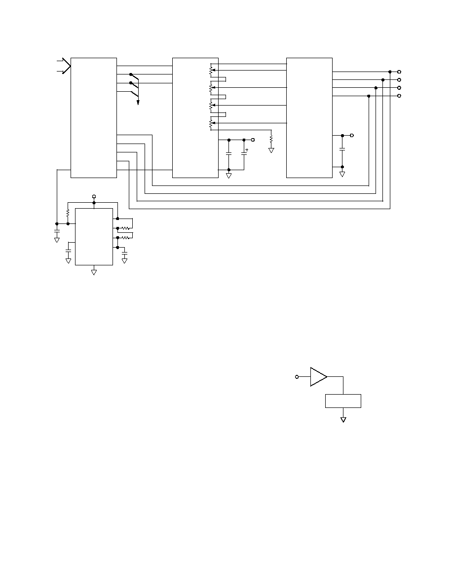
Intelligent Temperature Control System--Interfacing the
8051 C with the ADT14
Connecting the 8051, or any modern microcontroller, with the
ADT14 yields a powerful temperature control tool. For ex-
ample, by using digitally controlled resistors (AD8402/3), a user
may automatically set the temperature trip points via computer
or touch pad. The ADT14 outputs are fed back to the controller
allowing it to sense whether or not a setpoint has been exceeded.
The higher temperature trip-point data can then be used to turn
on a fan to either a high or low setting. In addition, the lower
temperature trip-point data may be used to turn on a heater to
either a high or low setting.
The AD8403 is shown in a single ladder resistor configuration
with an additional fix resistor to set the voltages of all four
setpoints. The microcontroller program that runs the AD8403
can also be set to ensure that no out-of-bound conditions occur.
Finally, the AD8403 also has shutdown pin which, when acti-
vated, will lower power consumption to 5
µ
A max (0.01
µ
A
typical), while still retaining memory of the potentiometer set-
tings.
Power-Down in Battery Powered Applications
Battery powered applications require low power consumption
components. The ADT14 is just such a device. The low supply
current (< 600
µ
A) of the ADT14 makes it possible to power
the device from any suitable logic output pin. Figure 29 is a
schematic of an 'HC04 CMOS inverter driving the ADT14. When
the SLEEP pin is high, the ADT14 is powered down. Figure 5
shows a typical start-up response of an ADT14. Most tempera-
ture measurements vary slowly over time, which allows designs
P3.2
P3.1
P3.0
P3.3
P2.0
P2.1
P2.2
P2.3
P2.4
P1.0/INT2
P0.0 TO
P0.7
USER
INPUTS
CS
CLK
SDI
SHDN
V
DD
GND
10 F
+5V
2.5V
REF
SET1
SET2
SET3
SET4
HYS
TRIP1
TRIP2
TRIP3
TRIP4
V
DD
GND
+5V
0.1 F
ADT14
AD8403
80CL51 C
TO 2ND
AD8403
RS
DIS
THR
TRIG
OUT
CONT
TLC555
V
CC
GND
+5V
0.1 F
0.1 F
NC
NC = NO CONNECT
Figure 28. Typical Microcontroller Setup Configuration
that consume very little power over very long periods of time by
using a duty-cycling technique. The basic idea of the duty-
cycling technique is to simply measure the temperature at se-
lected time intervals and leave the device powered down the rest
of the time. Instead of a CMOS inverter, any other logic pin
with sufficient drive capability (such as the output of a micro-
processor) can be used to power on and off the ADT14.
ADT14
V+
'HC04
SLEEP
Figure 29. Using a CMOS Inverter to Power Down the
ADT14
Combining Trip Point Outputs to Yield 25%, 50%, 75%, and
100% Power Outputs
It is often desirable to power a device at varying levels based
upon ambient temperature. For example, suppose a liquid is
below a desired temperature, the lowest trip point temperature.
In this case, full power should be delivered to the heating ele-
ment, causing the temperature to rise as rapidly as possible.
When the lowest trip-point is finally crossed, a reduction in
power should occur, slowing the rate of increase in the heating
process. This process continues until all trip points are crossed
and the current to the heating element is reduced to zero.
ADT14
15
REV. 0
Figure 30 illustrates the system described in the previous para-
graph, where each trip-point output corresponds to a 25% re-
duction in power when tripped. This is accomplished by the
dual rail-to-rail precision OP284 op amp configured as an in-
verting summer in the first stage, and as a V/I converter in the
second stage.
Suppose, however, that the heating element at a reduced power
level is unable to raise the ambient temperature to the desired
setting. This issue can be addressed by using a microcontroller
as shown in Figure 28. The microcontroller allows the time for
the given volume of material to heat up from a low trip-point
temperature to the next highest temperature trip-point to be
measured. If this time is too long, the microcontroller could add
additional power to the heater by altering a setpoint level.
1/2 OP284
1/2 OP284
10k
10k
10k
10k
2.49k
ADT14
TRIP4 (0%)
TRIP3 (25%)
TRIP2 (50%)
TRIP1 (75%)
2.5V
REF
V
CC
+5V
+5V
+5V
HEATING
ELEMENT
Q1
Figure 30. Combination Trip-Point Output
ADT14
16
REV. 0
C3067125/97
PRINTED IN U.S.A.
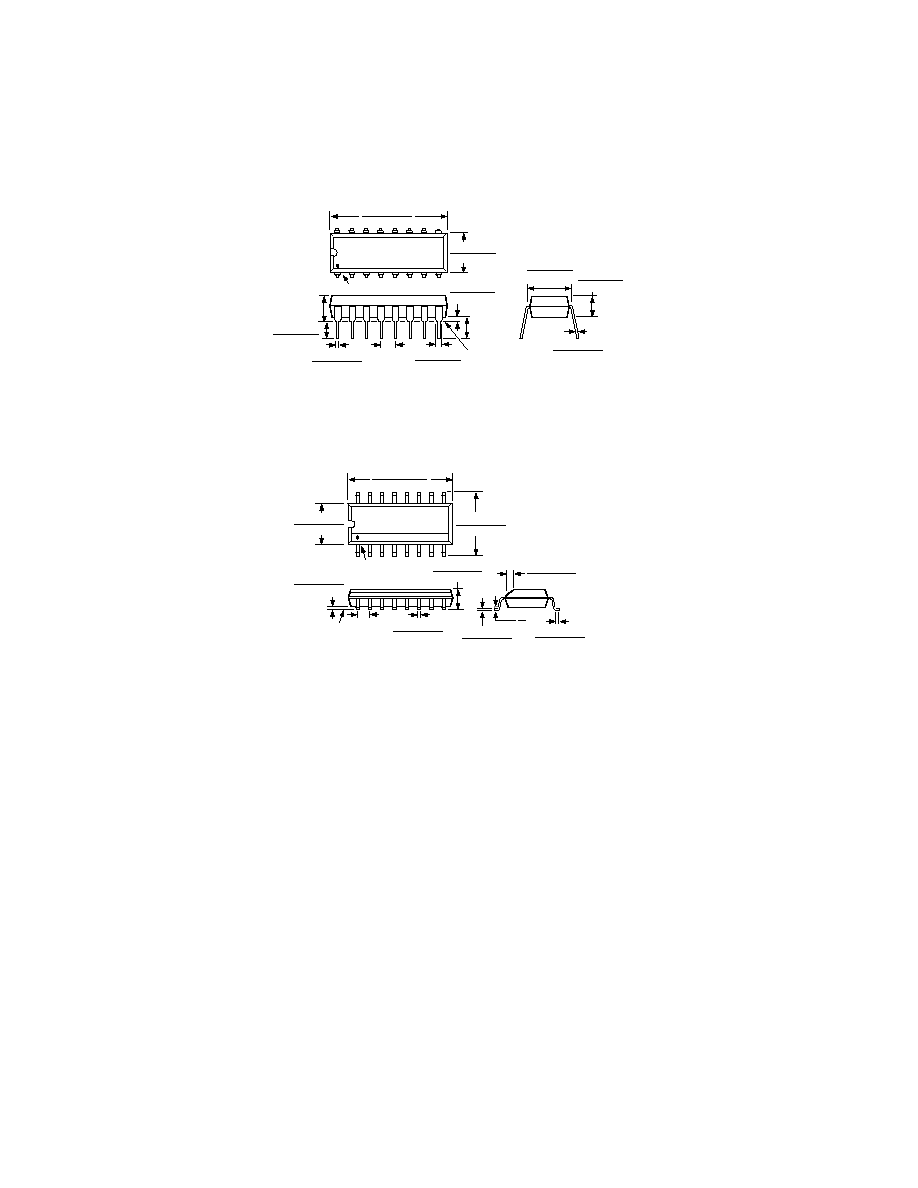
OUTLINE DIMENSIONS
Dimensions shown in inches and (mm).
16-Lead Plastic DIP
(N-16)
16
1
8
9
0.840 (21.34)
0.745 (18.92)
0.280 (7.11)
0.240 (6.10)
PIN 1
SEATING
PLANE
0.022 (0.558)
0.014 (0.356)
0.060 (1.52)
0.015 (0.38)
0.210 (5.33)
MAX
0.130
(3.30)
MIN
0.070 (1.77)
0.045 (1.15)
0.100
(2.54)
BSC
0.160 (4.06)
0.115 (2.93)
0.325 (8.26)
0.300 (7.62)
0.015 (0.381)
0.008 (0.204)
0.195 (4.95)
0.115 (2.93)
16-Lead Narrow-Body SOIC
(R-16A)
16
9
8
1
0.3937 (10.00)
0.3859 (9.80)
0.2440 (6.20)
0.2284 (5.80)
0.1574 (4.00)
0.1497 (3.80)
PIN 1
SEATING
PLANE
0.0098 (0.25)
0.0040 (0.10)
0.0192 (0.49)
0.0138 (0.35)
0.0688 (1.75)
0.0532 (1.35)
0.0500
(1.27)
BSC
0.0099 (0.25)
0.0075 (0.19)
0.0500 (1.27)
0.0160 (0.41)
8
°
0
°
0.0196 (0.50)
0.0099 (0.25)
x 45
°