Äîêóìåíòàöèÿ è îïèñàíèÿ www.docs.chipfind.ru
a
Blackfin
®
Embedded Processor
Information furnished by Analog Devices is believed to be accurate and reliable. How-
ever, no responsibility is assumed by Analog Devices for its use, nor for any
infringements of patents or other rights of third parties that may result from its use. No
license is granted by implication or otherwise under any patent or patent rights of Analog
Devices. Trademarks and registered trademarks are the property of their respective
owners.
REV. A
Blackfin and the Blackfin logo are registered trademarks of Analog Devices, Inc.
ADSP-BF535
KEY FEATURES
350 MHz High Performance Blackfin Processor Core
Two 16-Bit MACs, Two 40-Bit ALUs, One 40-Bit Shifter,
Four 8-Bit Video ALUs, and Two 40-Bit Accumulators
RISC-Like Register and Instruction Model for Ease of
Programming and Compiler Friendly Support
Advanced Debug, Trace, and Performance Monitoring
1.0 V1.6 V Core V
DD
with Dynamic Power Management
3.3 V I/O
260-Ball PBGA Package
MEMORY
308K Bytes of On-Chip Memory:
16K Bytes of Instruction L1 SRAM/Cache
32K Bytes of Data L1 SRAM/Cache
4K Bytes of Scratch Pad L1 SRAM
256K Bytes of Full Speed, Low Latency L2 SRAM
Memory DMA Controller
Memory Management Unit for Memory Protection
Glueless External Memory Controllers
Synchronous SDRAM Support
Asynchronous with SRAM, Flash, ROM Support
PERIPHERALS
32-Bit, 33 MHz, 3.3 V, PCI 2.2 Compliant Bus Interface
with Master and Slave Support
Integrated USB 1.1 Compliant Device Interface
Two UARTs, One with IrDA
®
Two SPI Compatible Ports
Two Full-Duplex Synchronous Serial Ports (SPORTs)
Four Timer/Counters, Three with PWM Support
Sixteen Bidirectional Programmable Flag I/O Pins
Watchdog Timer
Real-Time Clock
On-Chip PLL with 1 to 31 Frequency Multiplier
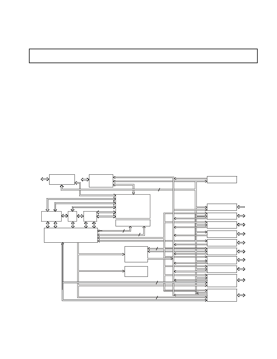
FUNCTIONAL BLOCK DIAGRAM
SYSTEM BUS
INTERFACE UNIT
DMA
CONTROLLER
PCI BUS INTERFACE
256K BYTES L2 SRAM
64
INTERRUPT
CONTROLLER/
TIMER
REAL-TIME CLOCK
UART PORT 1
UART PORT 0
IrDA
TIMER0, TIMER1,
TIMER2
PROGRAMMABLE
FLAGS
USB INTERFACE
SERIAL PORTS (2)
SPI PORTS (2)
EXTERNAL PORT
FLASH SDRAM
CONTROL
BOOT ROM
32
32
32
JTAG TEST AND
EMULATION
WATCHDOG TIMER
32
32
L1
DATA
MEMORY
MMU
L1
INSTRUCTION
MEMORY
B
One Technology Way, P.O. Box 9106, Norwood, MA 02062-9106 U.S.A.
Tel:781/329-4700
www.analog.com
Fax:781/326-8703
© 2004 Analog Devices, Inc. All rights reserved.
.

ADSP-BF535
2
REV. A
TABLE OF CONTENTS
GENERAL DESCRIPTION . . . . . . . . . . . . . . . . . . . . 2
Portable Low Power Architecture . . . . . . . . . . . . . . . 2
System Integration . . . . . . . . . . . . . . . . . . . . . . . . . . . 2
ADSP-BF535 Peripherals . . . . . . . . . . . . . . . . . . . . . 3
Processor Core . . . . . . . . . . . . . . . . . . . . . . . . . . . . . 3
Memory Architecture . . . . . . . . . . . . . . . . . . . . . . . . 4
Internal (On-Chip) Memory . . . . . . . . . . . . . . . . . . 5
External (Off-Chip) Memory . . . . . . . . . . . . . . . . . 5
PCI . . . . . . . . . . . . . . . . . . . . . . . . . . . . . . . . . . . . 5
I/O Memory Space . . . . . . . . . . . . . . . . . . . . . . . . . 5
Booting . . . . . . . . . . . . . . . . . . . . . . . . . . . . . . . . . 6
Event Handling . . . . . . . . . . . . . . . . . . . . . . . . . . . 6
Core Event Controller (CEC) . . . . . . . . . . . . . . . . 6
System Interrupt Controller (SIC) . . . . . . . . . . . . . 6
Event Control . . . . . . . . . . . . . . . . . . . . . . . . . . . . 7
DMA Controllers . . . . . . . . . . . . . . . . . . . . . . . . . . . 7
External Memory Control . . . . . . . . . . . . . . . . . . . . . 8
PC133 SDRAM Controller . . . . . . . . . . . . . . . . . . 8
Asynchronous Controller . . . . . . . . . . . . . . . . . . . . 8
PCI Interface . . . . . . . . . . . . . . . . . . . . . . . . . . . . . . . 8
PCI Host Function . . . . . . . . . . . . . . . . . . . . . . . . . 8
PCI Target Function . . . . . . . . . . . . . . . . . . . . . . . 8
USB Device . . . . . . . . . . . . . . . . . . . . . . . . . . . . . . . . 8
Real-Time Clock . . . . . . . . . . . . . . . . . . . . . . . . . . . . 9
Watchdog Timer . . . . . . . . . . . . . . . . . . . . . . . . . . . . 9
Timers . . . . . . . . . . . . . . . . . . . . . . . . . . . . . . . . . . . . 9
Serial Ports (Sports) . . . . . . . . . . . . . . . . . . . . . . . . . 9
Serial Peripheral Interface (SPI) Ports . . . . . . . . . . . 10
UART Port . . . . . . . . . . . . . . . . . . . . . . . . . . . . . . . 10
Programmable Flags (PFX) . . . . . . . . . . . . . . . . . . . 11
Dynamic Power Management . . . . . . . . . . . . . . . . . 11
Full On Operating Mode
Maximum Performance . . . . . . . . . . . . . . . . . 11
Active Operating Mode
Moderate Power Savings . . . . . . . . . . . . . . . . 11
Sleep Operating Mode
High Power Savings . . . . . . . . . . . . . . . . . . . . 11
Deep Sleep Operating Mode
Maximum Power Savings . . . . . . . . . . . . . . . . 12
Mode Transitions . . . . . . . . . . . . . . . . . . . . . . . . . 12
Power Savings . . . . . . . . . . . . . . . . . . . . . . . . . . . 12
Peripheral Power Control . . . . . . . . . . . . . . . . . . . 13
Clock Signals . . . . . . . . . . . . . . . . . . . . . . . . . . . . . . 13
Booting Modes . . . . . . . . . . . . . . . . . . . . . . . . . . . . 14
Instruction Set Description . . . . . . . . . . . . . . . . . . . 14
Development Tools . . . . . . . . . . . . . . . . . . . . . . . . . 15
EZ-KITLiteTM forADSP-BF535 Blackfin Processor 16
Designing an Emulator Compatible
Processor Board (Target) . . . . . . . . . . . . . . . . . 16
Additional Information . . . . . . . . . . . . . . . . . . . . . . 16
PIN DESCRIPTIONS . . . . . . . . . . . . . . . . . . . . . . . . 17
Unused Pins . . . . . . . . . . . . . . . . . . . . . . . . . . . . . . 20
SPECIFICATIONS . . . . . . . . . . . . . . . . . . . . . . . . . . 21
ABSOLUTE MAXIMUM RATINGS . . . . . . . . . . 22
ESD SENSITIVITY . . . . . . . . . . . . . . . . . . . . . . . . 22
TIMING SPECIFICATIONS . . . . . . . . . . . . . . . . 23
Clock and Reset Timing . . . . . . . . . . . . . . . . . . . . 24
Programmable Flags Cycle Timing . . . . . . . . . . . 25
Timer PWM_OUT Cycle Timing . . . . . . . . . . . . 26
Asynchronous Memory Write Cycle Timing . . . . 27
Asynchronous Memory Read Cycle Timing . . . . . 28
SDRAM Interface Timing . . . . . . . . . . . . . . . . . . 29
Serial Ports . . . . . . . . . . . . . . . . . . . . . . . . . . . . . 30
Serial Peripheral Interface (SPI) Port
--Master Timing . . . . . . . . . . . . . . . . . . . . . . . 32
Serial Peripheral Interface (SPI) Port
--Slave Timing . . . . . . . . . . . . . . . . . . . . . . . . . 33
Universal Asynchronous Receiver-Transmitter
(UART) Port--Receive and Transmit Timing . 34
JTAG Test and Emulation Port Timing . . . . . . . . 35
Output Drive Currents . . . . . . . . . . . . . . . . . . . . 36
Power Dissipation . . . . . . . . . . . . . . . . . . . . . . . . 36
Test Conditions . . . . . . . . . . . . . . . . . . . . . . . . . . 37
Output Enable Time . . . . . . . . . . . . . . . . . . . . 37
Output Disable Time . . . . . . . . . . . . . . . . . . . . 37
Example System Hold Time Calculation . . . . . 37
Environmental Conditions . . . . . . . . . . . . . . . . . . 38
260-Ball PBGA Pinout . . . . . . . . . . . . . . . . . . . . . . 39
OUTLINE DIMENSIONS . . . . . . . . . . . . . . . . . . . . 44
ORDERING GUIDE . . . . . . . . . . . . . . . . . . . . . . . . 44
GENERAL DESCRIPTION
The ADSP-BF535 processor is a member of the Blackfin
processor family of products, incorporating the Micro Signal
Architecture (MSA), jointly developed by Analog Devices, Inc.
and Intel Corporation. The architecture combines a dual MAC
state-of-the-art signal processing engine, the advantages of a
clean, orthogonal RISC-like microprocessor instruction set, and
Single-Instruction, Multiple Data (SIMD) multimedia capabili-
ties into a single instruction set architecture.
By integrating a rich set of industry leading system peripherals
and memory, Blackfin processors are the platform of choice for
next generation applications that require RISC-like programma-
bility, multimedia support, and leading edge signal processing in
one integrated package.
Portable Low Power Architecture
Blackfin processors provide world class power management and
performance. Blackfin processors are designed in a low power
and low voltage design methodology and feature dynamic power
management, the ability to independently vary both the voltage
and frequency of operation to significantly lower overall power
consumption. Varying the voltage and frequency can result in a
substantial reduction in power consumption, by comparison to
just varying the frequency of operation. This translates into
longer battery life for portable appliances.
System Integration
The ADSP-BF535 Blackfin processor is a highly integrated
system-on-a-chip solution for the next generation of digital com-
munication and portable Internet appliances. By combining
industry-standard interfaces with a high performance signal
processing core, users can develop cost-effective solutions
quickly without the need for costly external components. The
ADSP-BF535 Blackfin processor system peripherals include
UARTs, SPIs, SPORTs, general-purpose Timers, a Real-Time
3
REV. A
ADSP-BF535
Clock, Programmable Flags, Watchdog Timer, and USB and
PCI buses for glueless peripheral expansion.
ADSP-BF535 Peripherals
The ADSP-BF535 Blackfin processor contains a rich set of
peripherals connected to the core via several high bandwidth
buses, providing flexibility in system configuration as well as
excellent overall system performance. See Functional Block
Diagram
on Page 1
. The base peripherals include general-
purpose functions such as UARTs, timers with PWM (Pulse
Width Modulation) and pulse measurement capability, general-
purpose flag I/O pins, a real-time clock, and a watchdog timer.
This set of functions satisfies a wide variety of typical system
support needs and is augmented by the system expansion capa-
bilities of the part. In addition to these general-purpose
peripherals, the ADSP-BF535 Blackfin processor contains high
speed serial ports for interfaces to a variety of audio and modem
CODEC functions. It also contains an event handler for flexible
management of interrupts from the on-chip peripherals and
external sources. And it contains power management control
functions to tailor the performance and power characteristics of
the processor and system to many application scenarios.
The on-chip peripherals can be easily augmented in many system
designs with little or no glue logic due to the inclusion of several
interfaces providing expansion on industry-standard buses.
These include a 32-bit, 33 MHz, V2.2 compliant PCI bus, SPI
serial expansion ports, and a device type USB port. These enable
the connection of a large variety of peripheral devices to tailor the
system design to specific applications with a minimum of design
complexity.
All of the peripherals, except for programmable flags, real-time
clock, and timers, are supported by a flexible DMA structure with
individual DMA channels integrated into the peripherals. There
is also a separate memory DMA channel dedicated to data
transfers between the various memory spaces including external
SDRAM and asynchronous memory, internal Level 1 and Level
2 SRAM, and PCI memory spaces. Multiple on-chip 32-bit
buses, running at up to 133 MHz, provide adequate bandwidth
to keep the processor core running along with activity on all of
the on-chip and external peripherals.
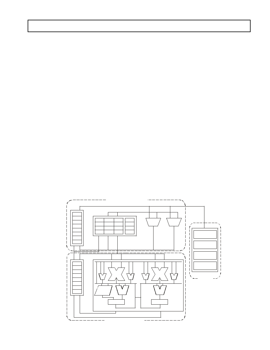
Processor Core
As shown in
Figure 1
, the Blackfin processor core contains two
multiplier/accumulators (MACs), two 40-bit ALUs, four video
ALUs, and a single shifter. The computational units process
8-bit, 16-bit, or 32-bit data from the register file.
Each MAC performs a 16-bit by 16-bit multiply in every cycle,
with an accumulation to a 40-bit result, providing 8 bits of
extended precision.
The ALUs perform a standard set of arithmetic and logical oper-
ations. With two ALUs capable of operating on 16- or 32-bit data,
the flexibility of the computation units covers the signal process-
ing requirements of a varied set of application needs. Each of the
two 32-bit input registers can be regarded as two 16-bit halves,
so each ALU can accomplish very flexible single 16-bit arithmetic
operations. By viewing the registers as pairs of 16-bit operands,
dual 16-bit or single 32-bit operations can be accomplished in a
single cycle. Quad 16-bit operations can be accomplished simply,
by taking advantage of the second ALU. This accelerates the per
cycle throughput.
Figure 1. Processor Core
SP
SEQU ENCE R
AL IGN
DEC ODE
L OOP BUF F ER
DA G0
D A G1
16
16
8
8
8
8
40
40
A0
A1
BA RR EL
SHIF T ER
DA T A AR ITH MET IC UN IT
CON TR OL
U NIT
ADD RESS A RIT HMET IC U NIT
FP
P5
P4
P3
P2
P1
P0
R7
R6
R5
R4
R3
R2
R1
R0
I3
I2
I1
I0
L3
L 2
L 1
L 0
B3
B2
B1
B0
M 3
M2
M1
M0
ADSP-BF535
4
REV. A
The powerful 40-bit shifter has extensive capabilities for perform-
ing shifting, rotating, normalization, extraction, and for
depositing data.
The data for the computational units is found in a multiported
register file of sixteen 16-bit entries or eight 32-bit entries.
A powerful program sequencer controls the flow of instruction
execution, including instruction alignment and decoding. The
sequencer supports conditional jumps and subroutine calls, as
well as zero-overhead looping. A loop buffer stores instructions
locally, eliminating instruction memory accesses for tightly
looped code.
Two data address generators (DAGs) provide addresses for
simultaneous dual operand fetches from memory. The DAGs
share a register file containing four sets of 32-bit Index, Modify,
Length, and Base registers. Eight additional 32-bit registers
provide pointers for general indexing of variables and stack
locations.
Blackfin processors support a modified Harvard architecture in
combination with a hierarchical memory structure. Level 1 (L1)
memories are those that typically operate at the full processor
speed with little or no latency. Level 2 (L2) memories are other
memories, on-chip or off-chip, that may take multiple processor
cycles to access. At the L1 level, the instruction memory holds
instructions only. The two data memories hold data, and a
dedicated scratch pad data memory stores stack and local variable
information. At the L2 level, there is a single unified memory
space, holding both instructions and data.
In addition, the L1 instruction memory and L1 data memories
may be configured as either Static RAMs (SRAMs) or caches.
The Memory Management Unit (MMU) provides memory pro-
tection for individual tasks that may be operating on the core and
may protect system registers from unintended access.
The architecture provides three modes of operation: user mode,
supervisor mode, and Emulation mode. User mode has restricted
access to certain system resources, thus providing a protected
software environment, while supervisor mode has unrestricted
access to the system and core resources.
The Blackfin processor instruction set has been optimized so that
16-bit op-codes represent the most frequently used instructions,
resulting in excellent compiled code density. Complex DSP
instructions are encoded into 32-bit op-codes, representing fully
featured multifunction instructions. Blackfin processors support
a limited multiple issue capability, where a 32-bit instruction can
be issued in parallel with two 16-bit instructions, allowing the
programmer to use many of the core resources in a single
instruction cycle.
The Blackfin processor assembly language uses an algebraic
syntax for ease of coding and readability. The architecture has
been optimized for use in conjunction with the C/C++ compiler,
resulting in fast and efficient software implementations.
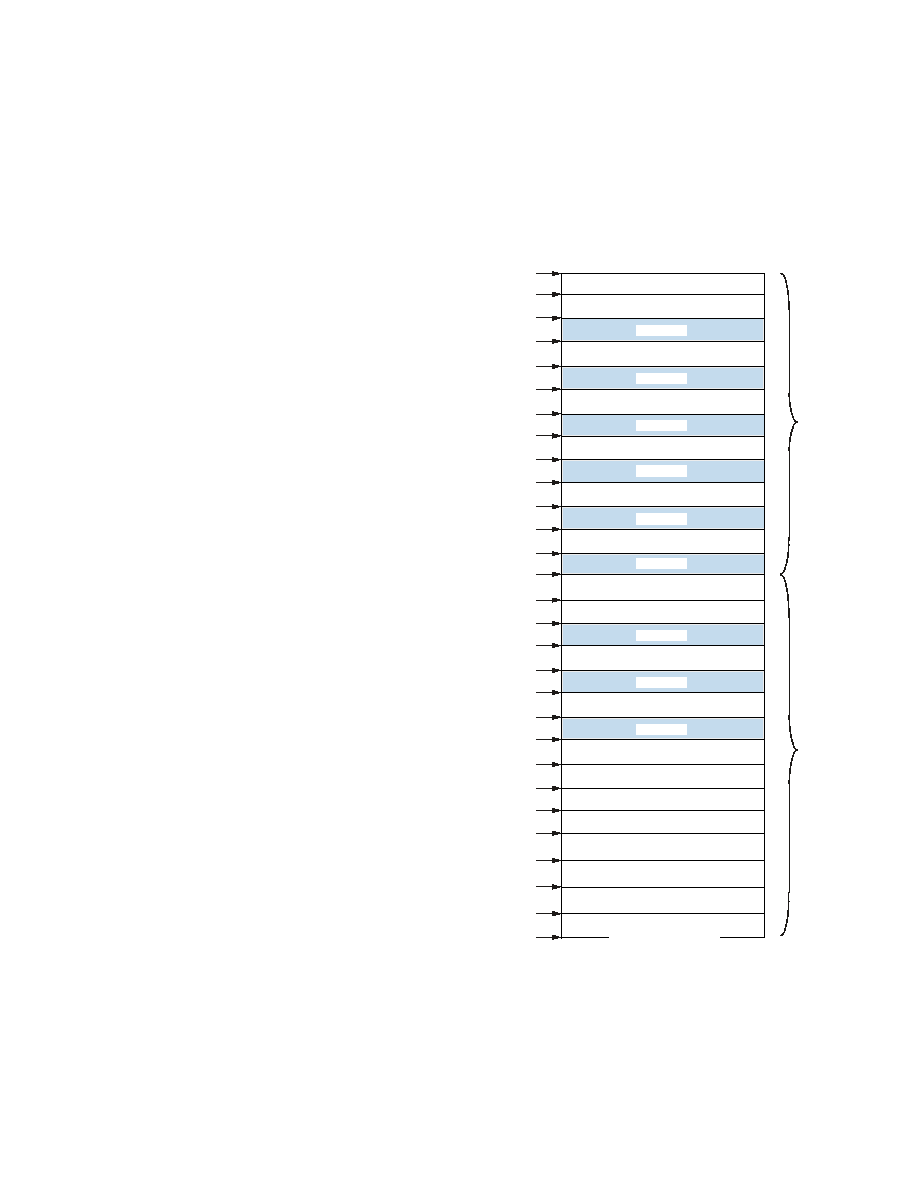
Memory Architecture
The ADSP-BF535 Blackfin processor views memory as a single
unified 4 Gbyte address space, using 32-bit addresses. All
resources, including internal memory, external memory, PCI
address spaces, and I/O control registers, occupy separate
sections of this common address space. The memory portions of
this address space are arranged in a hierarchical structure to
provide a good cost/performance balance with very fast, low
latency memory as cache or SRAM very close to the processor;
and larger, lower cost, and lower performance memory systems
farther away from the processor. See
Figure 2
.
Figure 2. Internal/External Memory Map
CORE MMR REGISTERS (2M BYTE)
I
N
T
E
R
N
A
L
M
E
M
O
R
Y
M
A
P
RESERVED
SCRATCHPAD SRAM (4K BYTE)
INSTRUCTION SRAM (16K BYTE)
SYSTEM MMR REGISTERS (2M BYTE)
RESERVED
RESERVED
DATA BANK B SRAM (16K BYTE)
RESERVED
DATA BANK A SRAM (16K BYTE)
RESERVED
L2 SRAM MEMORY (256K BYTE)
RESERVED
E
X
T
E
R
N
A
L
M
E
M
O
R
Y
M
A
P
PCI CONFIG SPACE PORT (4 BYTE)
PCI CONFIG REGISTERS (64K BYTE)
RESERVED
PCI IO SPACE (64K BYTE)
RESERVED
PCI MEMORY SPACE (128M BYTE)
RESERVED
ASYNC MEMORY BANK 3 (64M BYTE)
ASYNC MEMORY BANK 2 (64M BYTE)
ASYNC MEMORY BANK 1 (64M BYTE)
ASYNC MEMORY BANK 0 (64M BYTE)
SDRAM MEMORY BANK 3
(16M BYTE - 128M BYTE)
1
SDRAM MEMORY BANK 2
(16M BYTE - 128M BYTE)
1
SDRAM MEMORY BANK 1
(16M BYTE - 128M BYTE)
1
SDRAM MEMORY BANK 0
(16M BYTE - 128M BYTE)
1
0xFFFF FFFF
0xFFE0 0000
0xFFB0 0000
0xFFA0 4000
0xFFA0 0000
0xFF90 4000
0xFF90 0000
0xFF80 4000
0xFF80 0000
0xF003 FFFF
0xF000 0000
0xEF00 0000
0xEEFF FFFC
0xEEFF FF00
0xEEFE FFFF
0xEEFE 0000
0xE7FF FFFF
0xE000 0000
0x2FFF FFFF
0x2C00 0000
0x2800 0000
0x2400 0000
0x2000 0000
0x1800 0000
0x1000 0000
0x0800 0000
0x0000 0000
0xFFC0 0000
0xFFB0 1000
1
THE ADDRESSES SHOWN FOR THE SDRAM BANKS REFLECT A FULLY
POPULATED SDRAM ARRAY WITH 512M BYTES OF MEMORY. IF ANY BANK
CONTAINS LESS THAN 128M BYTES OF MEMORY, THAT BANK WOULD
EXTEND ONLY TO THE LENGTH OF THE REAL MEMORY SYSTEMS, AND THE
END ADDRESS WOULD BECOME THE START ADDRESS OF THE NEXT BANK.
THIS WOULD CONTINUE FOR ALL FOUR BANKS, WITH ANY REMAINING SPACE
BETWEEN THE END OF MEMORY BANK 3 AND THE BEGINNING OF ASYNC
MEMORY BANK 0, AT ADDRESS 0x2000 0000, TREATED AS RESERVED
ADDRESS SPACE.

5
REV. A
ADSP-BF535
The L1 memory system is the primary highest performance
memory available to the Blackfin processor core. The L2 memory
provides additional capacity with slightly lower performance.
Lastly, the off-chip memory system, accessed through the
External Bus Interface Unit (EBIU), provides expansion with
SDRAM, flash memory, and SRAM, optionally accessing more
than 768M bytes of external physical memory.
The memory DMA controller provides high bandwidth data-
movement capability. It can perform block transfers of code or
data between the internal L1/L2 memories and the external
memory spaces (including PCI memory space).
Internal (On-Chip) Memory
The ADSP-BF535 Blackfin processor has four blocks of on-chip
memory providing high bandwidth access to the core.
The first is the L1 instruction memory consisting of 16K bytes
of 4-Way set-associative cache memory. In addition, the memory
may be configured as an SRAM. This memory is accessed at full
processor speed.
The second on-chip memory block is the L1 data memory, con-
sisting of two banks of 16K bytes each. Each L1 data memory
bank can be configured as one Way of a 2-Way set-associative
cache or as an SRAM, and is accessed at full speed by the core.
The third memory block is a 4K byte scratch pad RAM which
runs at the same speed as the L1 memories, but is only accessible
as data SRAM (it cannot be configured as cache memory and is
not accessible via DMA).
The fourth on-chip memory system is the L2 SRAM memory
array which provides 256K bytes of high speed SRAM at the full
bandwidth of the core, and slightly longer latency than the L1
memory banks. The L2 memory is a unified instruction and data
memory and can hold any mixture of code and data required by
the system design.
The Blackfin processor core has a dedicated low latency 64-bit
wide datapath port into the L2 SRAM memory.
External (Off-Chip) Memory
External memory is accessed via the External Bus Interface Unit
(EBIU). This interface provides a glueless connection to up to
four banks of synchronous DRAM (SDRAM) as well as up to
four banks of asynchronous memory devices including flash,
EPROM, ROM, SRAM, and memory-mapped I/O devices.
The PC133 compliant SDRAM controller can be programmed
to interface to up to four banks of SDRAM, with each bank
containing between 16M bytes and 128M bytes providing access
to up to 512M bytes of SDRAM. Each bank is independently
programmable and is contiguous with adjacent banks regardless
of the sizes of the different banks or their placement. This allows
flexible configuration and upgradability of system memory while
allowing the core to view all SDRAM as a single, contiguous,
physical address space.
The asynchronous memory controller can also be programmed
to control up to four banks of devices with very flexible timing
parameters for a wide variety of devices. Each bank occupies a
64 Mbyte segment regardless of the size of the devices used so
that these banks will only be contiguous if fully populated with
64M bytes of memory.
PCI
The PCI bus defines three separate address spaces, which are
accessed through windows in the ADSP-BF535 Blackfin
processor memory space. These spaces are PCI memory, PCI
I/O, and PCI configuration.
In addition, the PCI interface can either be used as a bridge from
the processor core as the controlling CPU in the system, or as a
host port where another CPU in the system is the host and the
ADSP-BF535 is functioning as an intelligent I/O device on the
PCI bus.
When the ADSP-BF535 Blackfin processor acts as the system
controller, it views the PCI address spaces through its mapped
windows and can initialize all devices in the system and maintain
a map of the topology of the environment.
The PCI memory region is a 4 Gbyte space that appears on the
PCI bus and can be used to map memory I/O devices on the bus.
The ADSP-BF535 Blackfin processor uses a 128 Mbyte window
in memory space to see a portion of the PCI memory space. A
base address register is provided to position this window
anywhere in the 4 Gbyte PCI memory space while its position
with respect to the processor addresses remains fixed.
The PCI I/O region is also a 4 Gbyte space. However, most
systems and I/O devices only use a 64 Kbyte subset of this space
for I/O mapped addresses. The ADSP-BF535 Blackfin processor
implements a 64K byte window into this space along with a base
address register which can be used to position it anywhere in the
PCI I/O address space, while the window remains at the same
address in the processor's address space.
PCI configuration space is a limited address space, which is used
for system enumeration and initialization. This address space is
a very low performance communication mode between the
processor and PCI devices. The ADSP-BF535 Blackfin
processor provides a one-value window to access a single data
value at any address in PCI configuration space. This window is
fixed and receives the address of the value, and the value if the
operation is a write. Otherwise, the device returns the value into
the same address on a read operation.
I/O Memory Space
Blackfin processors do not define a separate I/O space. All
resources are mapped through the flat 32-bit address space.
On-chip I/O devices have their control registers mapped into
memory-mapped registers (MMRs) at addresses near the top of
the 4 Gbyte address space. These are separated into two smaller
blocks, one which contains the control MMRs for all core func-
tions, and the other which contains the registers needed for setup
and control of the on-chip peripherals outside of the core. The
core MMRs are accessible only by the core and only in supervisor
mode and appear as reserved space by on-chip peripherals, as
well as external devices accessing resources through the PCI bus.
The system MMRs are accessible by the core in supervisor mode
and can be mapped as either visible or reserved to other devices,
depending on the system protection model desired.

ADSP-BF535
6
REV. A
Booting
The ADSP-BF535 Blackfin processor contains a small boot
kernel, which configures the appropriate peripheral for booting.
If the ADSP-BF535 Blackfin processor is configured to boot from
boot ROM memory space, the processor starts executing from
the on-chip boot ROM. For more information, see
Booting
Modes on Page 14
.
Event Handling
The event controller on the ADSP-BF535 Blackfin processor
handles all asynchronous and synchronous events to the proces-
sor. The ADSP-BF535 Blackfin processor provides event
handling that supports both nesting and prioritization. Nesting
allows multiple event service routines to be active simultaneously.
Prioritization ensures that servicing of a higher-priority event
takes precedence over servicing of a lower priority event. The
controller provides support for five different types of events:
·
Emulation--An emulation event causes the processor to
enter emulation mode, allowing command and control of
the processor via the JTAG interface.
·
Reset--This event resets the processor.
·
Non-Maskable Interrupt (NMI)--The NMI event can be
generated by the software watchdog timer or by the NMI
input signal to the processor. The NMI event is frequently
used as a power-down indicator to initiate an orderly
shutdown of the system.
·
Exceptions--Events that occur synchronously to program
flow, for example, the exception will be taken before the
instruction is allowed to complete. Conditions such as
data alignment violations, undefined instructions, and so
on, cause exceptions.
·
Interrupts--Events that occur asynchronously to
program flow. They are caused by timers, peripherals,
input pins, explicit software instructions, and so on.
Each event has an associated register to hold the return address
and an associated return-from-event instruction. The state of the
processor is saved on the supervisor stack, when an event is
triggered.
The ADSP-BF535 Blackfin processor event controller consists
of two stages, the Core Event Controller (CEC) and the System
Interrupt Controller (SIC). The Core Event Controller works
with the System Interrupt Controller to prioritize and control all
system events. Conceptually, interrupts from the peripherals
enter into the SIC, and are then routed directly into the general-
purpose interrupts of the CEC.
Core Event Controller (CEC)
The CEC supports nine general-purpose interrupts (IVG157),
in addition to the dedicated interrupt and exception events. Of
these general-purpose interrupts, the two lowest priority inter-
rupts (IVG1514) are recommended to be reserved for software
interrupt handlers, leaving seven prioritized interrupt inputs to
support the peripherals of the ADSP-BF535 Blackfin processor.
Table 1
describes the inputs to the CEC, identifies their names
in the Event Vector Table (EVT), and lists their priorities.
System Interrupt Controller (SIC)
The System Interrupt Controller provides the mapping and
routing of events from the many peripheral interrupt sources to
the prioritized general-purpose interrupt inputs of the CEC.
Although the ADSP-BF535 Blackfin processor provides a default
mapping, the user can alter the mappings and priorities of
interrupt events by writing the appropriate values into the
Interrupt Assignment Registers (IAR).
Table 2
describes the
inputs into the SIC and the default mappings into the CEC.
Table 1. Core Event Controller (CEC)
Priority
(0 is Highest)
Event Class
EVT Entry
0
Emulation/Test
EMU
1
Reset
RST
2
Non-Maskable NMI
3
Exceptions
EVX
4
Global Enable
5
Hardware Error
IVHW
6
Core Timer
IVTMR
7
General Interrupt 7
IVG7
8
General Interrupt 8
IVG8
9
General Interrupt 9
IVG9
10
General Interrupt 10
IVG10
11
General Interrupt 11
IVG11
12
General Interrupt 12
IVG12
13
General Interrupt 13
IVG13
14
General Interrupt 14
IVG14
15
General Interrupt 15
IVG15
Table 2. System Interrupt Controller (SIC)
Peripheral Interrupt
Event
Peripheral
Interrupt ID
Default
Mapping
Real-Time Clock
0
IVG7
Reserved
1
USB 2
IVG7
PCI Interrupt
3
IVG7
SPORT 0 Rx DMA
4
IVG8
SPORT 0 Tx DMA
5
IVG8
SPORT 1 Rx DMA
6
IVG8
SPORT 1 Tx DMA
7
IVG8
SPI 0 DMA
8
IVG9
SPI 1 DMA
9
IVG9
UART 0 Rx
10
IVG10
UART 0 Tx
11
IVG10
UART 1 Rx
12
IVG10
UART 1 Tx
13
IVG10
Timer 0
14
IVG11
Timer 1
15
IVG11
Timer 2
16
IVG11
GPIO Interrupt A
17
IVG12
GPIO Interrupt B
18
IVG12

7
REV. A
ADSP-BF535
Event Control
The ADSP-BF535 Blackfin processor provides the user with a
very flexible mechanism to control the processing of events. In
the CEC, three registers are used to coordinate and control
events. Each of the registers is 16 bits wide, and each bit repre-
sents a particular event class:
·
CEC Interrupt Latch Register (ILAT)--The ILAT
register indicates when events have been latched. The
appropriate bit is set when the processor has latched the
event and cleared when the event has been accepted into
the system. This register is updated automatically by the
controller but may be read while in supervisor mode.
·
CEC Interrupt Mask Register (IMASK)--The IMASK
register controls the masking and unmasking of individual
events. When a bit is set in the IMASK register, that event
is unmasked and will be processed by the CEC when
asserted. A cleared bit in the IMASK register masks the
event thereby preventing the processor from servicing the
event even though the event may be latched in the ILAT
register. This register may be read from or written to while
in supervisor mode. (Note that general-purpose inter-
rupts can be globally enabled and disabled with the STI
and CLI instructions, respectively.)
·
CEC Interrupt Pending Register (IPEND)--The
IPEND register keeps track of all nested events. A set bit
in the IPEND register indicates the event is currently
active or nested at some level. This register is updated
automatically by the controller but may be read while in
supervisor mode.
The SIC allows further control of event processing by providing
three 32-bit interrupt control and status registers. Each register
contains a bit corresponding to each of the peripheral interrupt
events shown in
Table 2
.
·
SIC Interrupt Mask Register (SIC_IMASK)--This
register controls the masking and unmasking of each
peripheral interrupt event. When a bit is set in the register,
that peripheral event is unmasked and will be processed
by the system when asserted. A cleared bit in the register
masks the peripheral event thereby preventing the
processor from servicing the event.
·
SIC Interrupt Status Register (SIC_ISTAT)--As
multiple peripherals can be mapped to a single event, this
register allows the software to determine which peripheral
event source triggered the interrupt. A set bit indicates
the peripheral is asserting the interrupt, a cleared bit
indicates the peripheral is not asserting the event.
·
SIC Interrupt Wakeup Enable Register (SIC_IWR)--By
enabling the corresponding bit in this register, each
peripheral can be configured to wake up the processor,
should the processor be in a powered down mode when
the event is generated. (
See Dynamic Power Management
on Page 11.
)
Because multiple interrupt sources can map to a single general-
purpose interrupt, multiple pulse assertions can occur
simultaneously, before or during interrupt processing for an
interrupt event already detected on this interrupt input. The
IPEND register contents are monitored by the SIC as the
interrupt acknowledgement.
The appropriate ILAT register bit is set when an interrupt rising
edge is detected (detection requires two core clock cycles). The
bit is cleared when the respective IPEND register bit is set. The
IPEND bit indicates that the event has entered into the processor
pipeline. At this point, the CEC will recognize and queue the next
rising edge event on the corresponding event input. The
minimum latency from the rising edge transition of the general-
purpose interrupt to the IPEND output asserted is three core
clock cycles; however, the latency can be much higher, depending
on the activity within and the mode of the processor.
DMA Controllers
The ADSP-BF535 Blackfin processor has multiple, independent
DMA controllers that support automated data transfers with
minimal overhead for the Blackfin processor core. DMA transfers
can occur between the ADSP-BF535 Blackfin processor's
internal memories and any of its DMA-capable peripherals.
Additionally, DMA transfers can be accomplished between any
of the DMA-capable peripherals and external devices connected
to the external memory interfaces, including the SDRAM con-
troller, the asynchronous memory controller and the PCI bus
interface. DMA-capable peripherals include the SPORTs, SPI
ports, UARTs, and USB port. Each individual DMA-capable
peripheral has at least one dedicated DMA channel. DMA to and
from PCI is accomplished by the memory DMA channel.
To describe each DMA sequence, the DMA controller uses a set
of parameters called a descriptor block. When successive DMA
sequences are needed, these descriptor blocks can be linked or
chained together, so the completion of one DMA sequence auto-
initiates and starts the next sequence. The descriptor blocks
include full 32-bit addresses for the base pointers for source and
destination, enabling access to the entire ADSP-BF535 Blackfin
processor address space.
In addition to the dedicated peripheral DMA channels, there is
a separate memory DMA channel provided for transfers between
the various memories of the ADSP-BF535 Blackfin processor
system. This enables transfers of blocks of data between any of
the memories, including on-chip Level 2 memory, external
SDRAM, ROM, SRAM, and flash memory, and PCI address
spaces with little processor intervention.
Memory DMA
19
IVG13
Software Watchdog Timer
20
IVG13
Reserved
26 21
Software Interrupt 1
27
IVG14
Software Interrupt 2
28
IVG15
Table 2. System Interrupt Controller (SIC) (continued)
Peripheral Interrupt
Event
Peripheral
Interrupt ID
Default
Mapping

ADSP-BF535
8
REV. A
External Memory Control
The External Bus Interface Unit (EBIU) on the ADSP-BF535
Blackfin processor provides a high performance, glueless
interface to a wide variety of industry-standard memory devices.
The controller is made up of two sections: the first is an SDRAM
controller for connection of industry-standard synchronous
DRAM devices and DIMMs (Dual Inline Memory Module),
while the second is an asynchronous memory controller intended
to interface to a variety of memory devices.
PC133 SDRAM Controller
The SDRAM controller provides an interface to up to four
separate banks of industry-standard SDRAM devices or
DIMMs, at speeds up to f
SCLK
. Fully compliant with the PC133
SDRAM standard, each bank can be configured to contain
between 16M bytes and 128M bytes of memory.
The controller maintains all of the banks as a contiguous address
space so that the processor sees this as a single address space,
even if different size devices are used in the different banks. This
enables a system design where the configuration can be upgraded
after delivery with either similar or different memories.
A set of programmable timing parameters is available to configure
the SDRAM banks to support slower memory devices. The
memory banks can be configured as either 32 bits wide for
maximum performance and bandwidth or 16 bits wide for
minimum device count and lower system cost.
All four banks share common SDRAM control signals and have
their own bank select lines providing a completely glueless
interface for most system configurations.
The SDRAM controller address, data, clock, and command pins
can drive loads up to 50 pF. For larger memory systems, the
SDRAM controller external buffer timing should be selected and
external buffering should be provided so that the load on the
SDRAM controller pins does not exceed 50 pF.
Asynchronous Controller
The asynchronous memory controller provides a configurable
interface for up to four separate banks of memory or I/O devices.
Each bank can be independently programmed with different
timing parameters, enabling connection to a wide variety of
memory devices including SRAM, ROM, and flash EPROM, as
well as I/O devices that interface with standard memory control
lines. Each bank occupies a 64 Mbyte window in the processor's
address space but, if not fully populated, these windows are not
made contiguous by the memory controller logic. The banks can
also be configured as 16-bit wide or 32-bit wide buses for ease of
interfacing to a range of memories and I/O devices tailored either
to high performance or to low cost and power.
PCI Interface
The ADSP-BF535 Blackfin processor provides a glueless logical
and electrical, 33 MHz, 3.3 V, 32-bit PCI (Peripheral
Component Interconnect), Revision 2.2 compliant interface.
The PCI interface is designed for a 3 V signalling environment.
The PCI interface provides a bus bridge function between the
processor core and on-chip peripherals and an external PCI bus.
The PCI interface of the ADSP-BF535 Blackfin processor
supports two PCI functions:
·
A host to PCI bridge function, in which the ADSP-BF535
Blackfin processor resources (the processor core, internal
and external memory, and the memory DMA controller)
provide the necessary hardware components to emulate
a host computer PCI interface, from the perspective of a
PCI target device.
·
A PCI target function, in which an ADSP-BF535 Blackfin
processor based intelligent peripheral can be designed to
easily interface to a Revision 2.2 compliant PCI bus.
PCI Host Function
As the PCI host, the ADSP-BF535 Blackfin processor provides
the necessary PCI host (platform) functions required to support
and control a variety of off-the-shelf PCI I/O devices (for
example, Ethernet controllers, bus bridges, and so on) in a system
in which the ADSP-BF535 Blackfin processor is the host.
Note that the Blackfin processor architecture defines only
memory space (no I/O or configuration address spaces). The
three address spaces of PCI space (memory, I/O, and configura-
tion space) are mapped into the flat 32-bit memory space of the
ADSP-BF535 Blackfin processor. Because the PCI memory
space is as large as the ADSP-BF535 Blackfin processor memory
address space, a windowed approach is employed, with separate
windows in the ADSP-BF535 Blackfin processor address space
used for accessing the three PCI address spaces. Base address
registers are provided so that these windows can be positioned to
view any range in the PCI address spaces while the windows
remain fixed in position in the ADSP-BF535 Blackfin processor's
address range.
For devices on the PCI bus viewing the ADSP-BF535 Blackfin
processor's resources, several mapping registers are provided to
enable resources to be viewed in the PCI address space. The
ADSP-BF535 Blackfin processor's external memory space,
internal L2, and some I/O MMRs can be selectively enabled as
memory spaces that devices on the PCI bus can use as targets for
PCI memory transactions.
PCI Target Function
As a PCI target device, the PCI host processor can configure the
ADSP-BF535 Blackfin processor subsystem during enumeration
of the PCI bus system. Once configured, the ADSP-BF535
Blackfin processor subsystem acts as an intelligent I/O device.
When configured as a target device, the PCI controller uses the
memory DMA controller to perform DMA transfers as required
by the PCI host.
USB Device
The ADSP-BF535 Blackfin processor provides a USB 1.1
compliant device type interface to support direct connection to
a host system. The USB core interface provides a flexible pro-
grammable environment with up to eight endpoints. Each
endpoint can support all of the USB data types including control,
bulk, interrupt, and isochronous. Each endpoint provides a
memory-mapped buffer for transferring data to the application.
The ADSP-BF535 Blackfin processor USB port has a dedicated

9
REV. A
ADSP-BF535
DMA controller and interrupt input to minimize processor
polling overhead and to enable asynchronous requests for CPU
attention only when transfer management is required.
The USB device requires an external 48 MHz oscillator. The
value of SCLK must always exceed 48 MHz for proper USB
operation.
Real-Time Clock
The ADSP-BF535 Blackfin processor Real-Time Clock (RTC)
provides a robust set of digital watch features, including current
time, stopwatch, and alarm. The RTC is clocked by a 32.768 kHz
crystal external to the ADSP-BF535 Blackfin processor. The
RTC peripheral has dedicated power supply pins, so that it can
remain powered up and clocked, even when the rest of the
processor is in a low power state. The RTC provides several
programmable interrupt options, including interrupt per second,
minute, or day clock ticks, interrupt on programmable stopwatch
countdown, or interrupt at a programmed alarm time.
The 32.768 kHz input clock frequency is divided down to a 1 Hz
signal by a prescaler. The counter function of the timer consists
of four counters: a 6-bit second counter, a 6-bit minute counter,
a 5-bit hours counter, and an 8-bit day counter.
When enabled, the alarm function generates an interrupt when
the output of the timer matches the programmed value in the
alarm control register. There are two alarms: one is for a time of
day, the second is for a day and time of that day.
The stopwatch function counts down from a programmed value,
with one minute resolution. When the stopwatch is enabled and
the counter underflows, an interrupt is generated.
Like the other peripherals, the RTC can wake up the ADSP-
BF535 Blackfin processor from a low power state upon
generation of any interrupt.
Connect RTC pins XTALI and XTALO with external compo-
nents, as shown in
Figure 3
.
Watchdog Timer
The ADSP-BF535 Blackfin processor includes a 32-bit timer,
which can be used to implement a software watchdog function.
A software watchdog can improve system availability by forcing
the processor to a known state, via generation of a hardware reset,
non-maskable interrupt (NMI), or general-purpose interrupt, if
the timer expires before being reset by software. The programmer
initializes the count value of the timer, enables the appropriate
interrupt, then enables the timer. Thereafter, the software must
reload the counter before it counts to zero from the programmed
value. This protects the system from remaining in an unknown
state where software, which would normally reset the timer, has
stopped running because of external noise conditions or a
software error.
After a reset, software can determine if the watchdog was the
source of the hardware reset by interrogating a status bit in the
timer control register, which is set only upon a watchdog
generated reset.
The timer is clocked by the system clock (SCLK), at a maximum
frequency of f
SCLK
.
Timers
There are four programmable timer units in the ADSP-BF535
Blackfin processor. Three general-purpose timers have an
external pin that can be configured either as a Pulse-Width
Modulator (PWM) or timer output, as an input to clock the
timer, or for measuring pulse widths of external events. Each of
the three general-purpose timer units can be independently pro-
grammed as a PWM, internally or externally clocked timer, or
pulse width counter.
The general-purpose timer units can be used in conjunction with
the UARTs to measure the width of the pulses in the data stream
to provide an autobaud detect function for a serial channel.
The general-purpose timers can generate interrupts to the
processor core providing periodic events for synchronization,
either to the processor clock or to a count of external signals.
In addition to the three general-purpose programmable timers,
a fourth timer is also provided. This extra timer is clocked by the
internal processor clock (CCLK) and is typically used as a system
tick clock for the generation of operating system periodic
interrupts.
Serial Ports (Sports)
The ADSP-BF535 Blackfin processor incorporates two complete
synchronous serial ports (SPORT0 and SPORT1) for serial and
multiprocessor communications. The SPORTs support these
features:
·
Bidirectional operation--Each SPORT has independent
transmit and receive pins.
·
Buffered (8-deep) transmit and receive ports--Each port
has a data register for transferring data-words to and from
other processor components and shift registers for shifting
data in and out of the data registers.
·
Clocking--Each transmit and receive port can either use
an external serial clock or generate its own, in frequencies
ranging from (f
SCLK
/131070) Hz to (f
SCLK
/2) Hz.
·
Word length--Each SPORT supports serial data-words
from 3 to 16 bits in length transferred in a format of most
significant bit first or least significant bit first.
Figure 3. External Components for RTC
XTAL0
C1
C2
X1
SUGGESTED COMPONENTS:
ECLIPTEK EC38J (THROUGH-HOLE PACKAGE)
EPSON MC405 12pF LOAD (SURFACE-MOUNT PACKAGE)
C1 = 22pF
C2 = 22pF
NOTE: C1 AND C2 ARE SPECIFIC TO CRYSTAL SPECIFIED FOR X1.
CONTACT CRYSTAL MANUFACTURER FOR DETAILS. C1 AND C2
SPECIFICATIONS ASSUME BOARD TRACE CAPACITANCE OF 3pF.
XTAL1

ADSP-BF535
10
REV. A
·
Framing--Each transmit and receive port can run with or
without frame sync signals for each data-word. Frame
sync signals can be generated internally or externally,
active high or low, with either of two pulse widths and
early or late frame sync.
·
Companding in hardware--Each SPORT can perform
A-law or µ-law companding according to ITU recommen-
dation G.711. Companding can be selected on the
transmit and/or receive channel of the SPORT without
additional latencies.
·
DMA operations with single-cycle overhead--Each
SPORT can automatically receive and transmit multiple
buffers of memory data. The Blackfin processor can link
or chain sequences of DMA transfers between a SPORT
and memory. The chained DMA can be dynamically
allocated and updated through the descriptor blocks that
set up the chain.
·
Interrupts--Each transmit and receive port generates an
interrupt upon completing the transfer of a data-word or
after transferring an entire data buffer or buffers through
the DMA.
·
Multichannel capability--Each SPORT supports 128
channels and is compatible with the H.100, H.110,
MVIP-90, and HMVIP standards.
Serial Peripheral Interface (SPI) Ports
The ADSP-BF535 Blackfin processor has two SPI compatible
ports that enable the processor to communicate with multiple
SPI compatible devices.
The SPI interface uses three pins for transferring data: two data
pins (Master Output-Slave Input, MOSIx, and Master Input-
Slave Output, MISOx) and a clock pin (Serial Clock, SCKx).
Two SPI chip select input pins (
SPISSx) let other SPI devices
select the processor, and fourteen SPI chip select output pins
(SPIxSEL71) let the processor select other SPI devices. The SPI
select pins are reconfigured programmable flag pins. Using these
pins, the SPI ports provide a full duplex, synchronous serial inter-
face, which supports both master and slave modes and
multimaster environments.
Each SPI port's baud rate and clock phase/polarities are program-
mable (see
Figure 4
), and each has an integrated DMA
controller, configurable to support transmit or receive data
streams. The SPI's DMA controller can only service unidirec-
tional accesses at any given time.
During transfers, the SPI ports simultaneously transmit and
receive by serially shifting data in and out on two serial data lines.
The serial clock line synchronizes the shifting and sampling of
data on the two serial data lines.
In master mode, the processor performs the following sequence
to set up and initiate SPI transfers:
1. Enables and configures the SPI port's operation (data
size and transfer format).
2. Selects the target SPI slave with an SPIxSELy output pin
(reconfigured programmable flag pin).
3. Defines one or more TCBs in the processor's memory
space (optional in DMA mode only).
4. Enables the SPI DMA engine and specifies transfer
direction (optional in DMA mode only).
5. Reads or writes the SPI port receive or transmit data
buffer (in non-DMA mode only).
The SCKx line generates the programmed clock pulses
for simultaneously shifting data out on MOSIx and
shifting data in on MISOx. In the DMA mode only,
transfers continue until the SPI DMA word count transi-
tions from 1 to 0.
In slave mode, the processor performs the following sequence to
set up the SPI port to receive data from a master transmitter:
1. Enables and configures the SPI slave port to match the
operation parameters set up on the master (data size and
transfer format) SPI transmitter.
2. Defines and generates a receive TCB in the processor's
memory space to interrupt at the end of the data transfer
(optional in DMA mode only).
3. Enables the SPI DMA engine for a receive access
(optional in DMA mode only).
4. Starts receiving data on the appropriate SPI SCKx edges
after receiving an SPI chip select on an
SPISSx input pin
(reconfigured programmable flag pin) from a master.
In DMA mode only, reception continues until the SPI DMA
word count transitions from 1 to 0. The processor can continue,
by queuing up the next command TCB.
A slave mode transmit operation is similar, except the processor
specifies the data buffer in memory from which to transmit data,
generates and relinquishes control of the transmit TCB, and
begins filling the SPI port's data buffer. If the SPI controller is
not ready to transmit, it can transmit a "zero" word.
UART Port
The ADSP-BF535 Blackfin processor provides two full-duplex
Universal Asynchronous Receiver/Transmitter (UART) ports
(UART0 and UART1) fully compatible with PC-standard
UARTs. The UART ports provide a simplified UART interface
to other peripherals or hosts, supporting full-duplex, DMA-sup-
ported, asynchronous transfers of serial data. Each UART port
Figure 4. SPI Clock Rate Calculation
SPI Clock Rate
f
SCLK
2
SPIBAUD
×
-------------------------------------
=

11
REV. A
ADSP-BF535
includes support for 5 to 8 data bits; 1 or 2 stop bits; and none,
even, or odd parity. The UART ports support two modes of
operation.
·
PIO (Programmed I/O)--The processor sends or receives
data by writing or reading I/O-mapped UATX or UARX
registers, respectively. The data is double-buffered on
both transmit and receive.
·
DMA (Direct Memory Access)--The DMA controller
transfers both transmit and receive data. This reduces the
number and frequency of interrupts required to transfer
data to and from memory. Each UART has two dedicated
DMA channels, one for transmit and one for receive. The
DMA channels have lower priority than most DMA
channels because of their relatively low service rates.
Each UART port's baud rate (see
Figure 5
), serial data format,
error code generation and status, and interrupts are
programmable:
·
Bit rates ranging from (f
SCLK
/1048576) to (f
SCLK
/16) bits
per second
·
Data formats from 7 to 12 bits per frame
·
Both transmit and receive operations can be configured
to generate maskable interrupts to the processor.
Autobaud detection is supported, in conjunction with the
general-purpose timer functions.
The capabilities of UART0 are further extended with support for
the Infrared Data Association (IrDA Serial Infrared Physical
Layer Link Specification (SIR) protocol.
Programmable Flags (PFX)
The ADSP-BF535 Blackfin processor has 16 bidirectional,
general-purpose I/O programmable flag (PF150) pins. The pro-
grammable flag pins have special functions for clock multiplier
selection, SROM boot mode, and SPI port operation. For more
information, see
Serial Peripheral Interface (SPI) Ports on
Page 10
and
Clock Signals on Page 13
. Each programmable flag
can be individually controlled by manipulation of the flag control,
status, and interrupt registers.
·
Flag Direction Control Register--Specifies the direction
of each individual PFx pin as input or output.
·
Flag Control and Status Registers--Rather than forcing
the software to use a read-modify-write process to control
the setting of individual flags, the ADSP-BF535 Blackfin
processor employs a "write one to set" and "write one to
clear" mechanism that allows any combination of individ-
ual flags to be set or cleared in a single instruction, without
affecting the level of any other flags. Two control registers
are provided, one register is written to in order to set flag
values while another register is written to in order to clear
flag values. Reading the flag status register allows software
to interrogate the sense of the flags.
·
Flag Interrupt Mask Registers--The two flag interrupt
mask registers allow each individual PFx pin to function
as an interrupt to the processor. Similar to the two flag
control registers that are used to set and clear individual
flag values, one flag interrupt mask register sets bits to
enable interrupt function, and the other flag interrupt
mask register clears bits to disable interrupt function. PFx
pins defined as inputs can be configured to generate
hardware interrupts, while output PFx pins can be con-
figured to generate software interrupts.
·
Flag Interrupt Sensitivity Registers--The two flag
interrupt sensitivity registers specify whether individual
PFx pins are level- or edge-sensitive and specify (if edge-
sensitive) whether just the rising edge or both the rising
and falling edges of the signal are significant. One register
selects the type of sensitivity, and one register selects
which edges are significant for edge-sensitivity.
Dynamic Power Management
The ADSP-BF535 Blackfin processor provides four operating
modes, each with a different performance/power dissipation
profile. In addition, dynamic power management provides the
control functions, with the appropriate external power regulation
capability to dynamically alter the processor core supply voltage,
further reducing power dissipation. Control of clocking to each
of the ADSP-BF535 Blackfin processor peripherals also reduces
power dissipation. See
Table 3
for a summary of the power
settings for each mode.
Full On Operating Mode
Maximum Performance
In the full on mode, the PLL is enabled, and is not bypassed,
providing the maximum operational frequency. This is the
normal execution state in which maximum performance can be
achieved. The processor core and all enabled peripherals run at
full speed.
Active Operating Mode
Moderate Power Savings
In the active mode, the PLL is enabled, but bypassed. The input
clock (CLKIN) is used to generate the clocks for the processor
core (CCLK) and peripherals (SCLK). When the PLL is
bypassed, CCLK runs at one-half the CLKIN frequency. Signif-
icant power savings can be achieved with the processor running
at one-half the CLKIN frequency. In this mode, the PLL multi-
plication ratio can be changed by setting the appropriate values
in the SSEL fields of the PLL control register (PLL_CTL).
When in the active mode, system DMA access to appropriately
configured L1 memory is supported.
Sleep Operating Mode
High Power Savings
The sleep mode reduces power dissipation by disabling the clock
to the processor core (CCLK). The PLL and system clock
(SCLK), however, continue to operate in this mode. Any inter-
rupt, typically via some external event or RTC activity, will wake
up the processor. When in sleep mode, assertion of any interrupt
will cause the processor to sense the value of the bypass bit
Figure 5. UART Clock Rate Calculation
UART Clock Rate
f
SCLK
16
D
×
-----------------
=
ADSP-BF535
12
REV. A
(BYPASS) in the PLL Control register (PLL_CTL). If bypass is
disabled, the processor transitions to the full on mode. If bypass
is enabled, the processor transitions to the Active mode.
When in Sleep mode, system DMA access to L1 memory is not
supported.
Deep Sleep Operating Mode
Maximum Power Savings
The deep sleep mode maximizes power savings by disabling the
clocks to the processor core (CCLK) and to all synchronous
peripherals (SCLK). Asynchronous peripherals, such as the
RTC, may still be running but will not be able to access internal
resources or external memory. This powered down mode can
only be exited by assertion of the reset interrupt (
RESET) or by
an asynchronous interrupt generated by the RTC. When in deep
sleep mode, assertion of
RESET causes the processor to sense
the value of the BYPASS pin. If bypass is disabled, the processor
will transition to full on mode. If bypass is enabled, the processor
will transition to active mode. When in deep sleep mode,
assertion of the RTC asynchronous interrupt causes the
processor to transition to the full on mode, regardless of the value
of the BYPASS pin.
The DEEPSLEEP output is asserted in this mode.
Mode Transitions
The available mode transitions diagrammed in
Figure 6
are
accomplished either by the interrupt events described in the
following sections or by programming the PLLCTL register with
the appropriate values and then executing the PLL programming
sequence.
This instruction sequence takes the processor to a known idle
state with the interrupts disabled. Note that all DMA activity
should be disabled during mode transitions.
Power Savings
As shown in
Table 4
, the ADSP-BF535 Blackfin processor
supports five different power domains. The use of multiple power
domains maximizes flexibility, while maintaining compliance
with industry standards and conventions. By isolating the internal
logic of the ADSP-BF535 Blackfin processor into its own power
domain, separate from the PLL, RTC, PCI, and other I/O, the
processor can take advantage of dynamic power management,
without affecting the PLL, RTC, or other I/O devices.
Table 3. Operating Mode Power Settings
Mode
PLL
PLL
Bypassed
Core Clock
(CCLK)
System Clock
(SCLK)
Full On
Enabled No
Enabled
Enabled
Active
Enabled Yes
Enabled
Enabled
Sleep
Enabled Yes or No Disabled
Enabled
Deep +
Disabled
Disabled
Disabled
Figure 6. Mode Transitions
STOPCK = 1
AND PDWN = 0
WAKEUP AND
BYPASS = 1
WAKEUP AND
BYPASS = 0
SLEEP
STOPCK = 1
AND PDWN = 0
FULL-ON
ACTIVE
PDWN = 1
PDWN = 1
BYPASS = 1
AND STOPCK = 0
AND PDWN = 0
RTC_WAKEUP
DEEP
SLEEP
HARDWARE
RESET
RESET
MSEL = NEW
AND PLL_OFF = 0
AND BYPASS = 1
MSEL = NEW
AND PLL_OFF = 0
AND BYPASS = 0
BYPASS = 0
AND PLL_OFF = 0
AND STOPCK = 0
AND PDWN = 0
Table 4. Power Domains
Power Domain
V
DD
Range
All internal logic, except PLL and RTC
V
DDINT
Analog PLL internal logic
V
DDPLL
RTC internal logic and crystal I/O
V
DDRTC
PCI I/O
V
DDPCIEXT
All other I/O
V
DDEXT
13
REV. A
ADSP-BF535
The power dissipated by a processor is largely a function of the
clock frequency of the processor and the square of the operating
voltage. For example, reducing the clock frequency by 25%
results in a 25% reduction in power dissipation, while reducing
the voltage by 25% reduces power dissipation by more than 40%.
Further, these power savings are additive, in that if the clock
frequency and power are both reduced, the power savings are
dramatic.
Dynamic Power Management allows both the processor's input
voltage (V
DDINT
) and clock frequency (f
CCLK
) to be dynamically
and independently controlled.
As previously explained, the savings in power dissipation can be
modeled by the following equation:
where:
is the nominal core clock frequency (300 MHz)
is the reduced core clock frequency
is the nominal internal supply voltage (1.5 V)
is the reduced internal supply voltage
As an example of how significant the power savings of Dynamic
Power Management are when both frequency and voltage are
reduced, consider an example where the frequency is reduced
from its nominal value to 50 MHz and the voltage is reduced from
its nominal value to 1.2 V. At this reduced frequency and voltage,
the processor dissipates about 10% of the power dissipated at
nominal frequency and voltage.
Peripheral Power Control
The ADSP-BF535 Blackfin processor provides additional power
control capability by allowing dynamic scheduling of clock inputs
to each of the peripherals. Clocking to each of the peripherals
listed below can be enabled or disabled by appropriately setting
the peripheral's control bit in the peripheral clock enable register
(PLL_IOCK). The Peripheral Clock Enable Register allows indi-
vidual control for each of these peripherals:
·
PCI
·
EBIU controller
·
Programmable flags
·
MemDMA controller
·
SPORT 0
·
SPORT 1
·
SPI 0
·
SPI 1
·
UART 0
·
UART 1
·
Timer 0, Timer 1, Timer 2
·
USB CLK
Clock Signals
The ADSP-BF535 Blackfin processor can be clocked by a sine
wave input or a buffered shaped clock derived from an external
clock oscillator.
If a buffered, shaped clock is used, this external clock connects
to the processor CLKIN pin. The CLKIN input cannot be
halted, changed, or operated below the specified frequency
during normal operation. This clock signal should be a 3.3 V
LVTTL compatible signal. The processor provides a user-pro-
grammable 1 to 31 multiplication of the input clock to
support external-to-internal clock ratios. The MSEL60,
BYPASS, and DF pins decide the PLL multiplication factor at
reset. At run time, the multiplication factor can be controlled in
software. The combination of pull-up and pull-down resistors in
Figure 7
sets up a core clock ratio of 6:1, which, for example,
produces a 150 MHz core clock from the 25 MHz input. For
other clock multiplier settings, see the ADSP-BF535 Blackfin
Processor Hardware Reference.
All on-chip peripherals operate at the rate set by the system clock
(SCLK). The system clock frequency is programmable by means
of the SSEL pins. At run time the system clock frequency can be
controlled in software by writing to the SSEL fields in the PLL
control register (PLL_CTL). The values programmed into the
Power Dissipation Factor
f
CCLKRED
f
CCLKNOM
--------------------------
V
DDINTRED
V
DDINTNOM
------------------------------
2
×
=
f
CCLKNOM
f
CCLKRED
V
DDINTNOM
V
DDINTRED
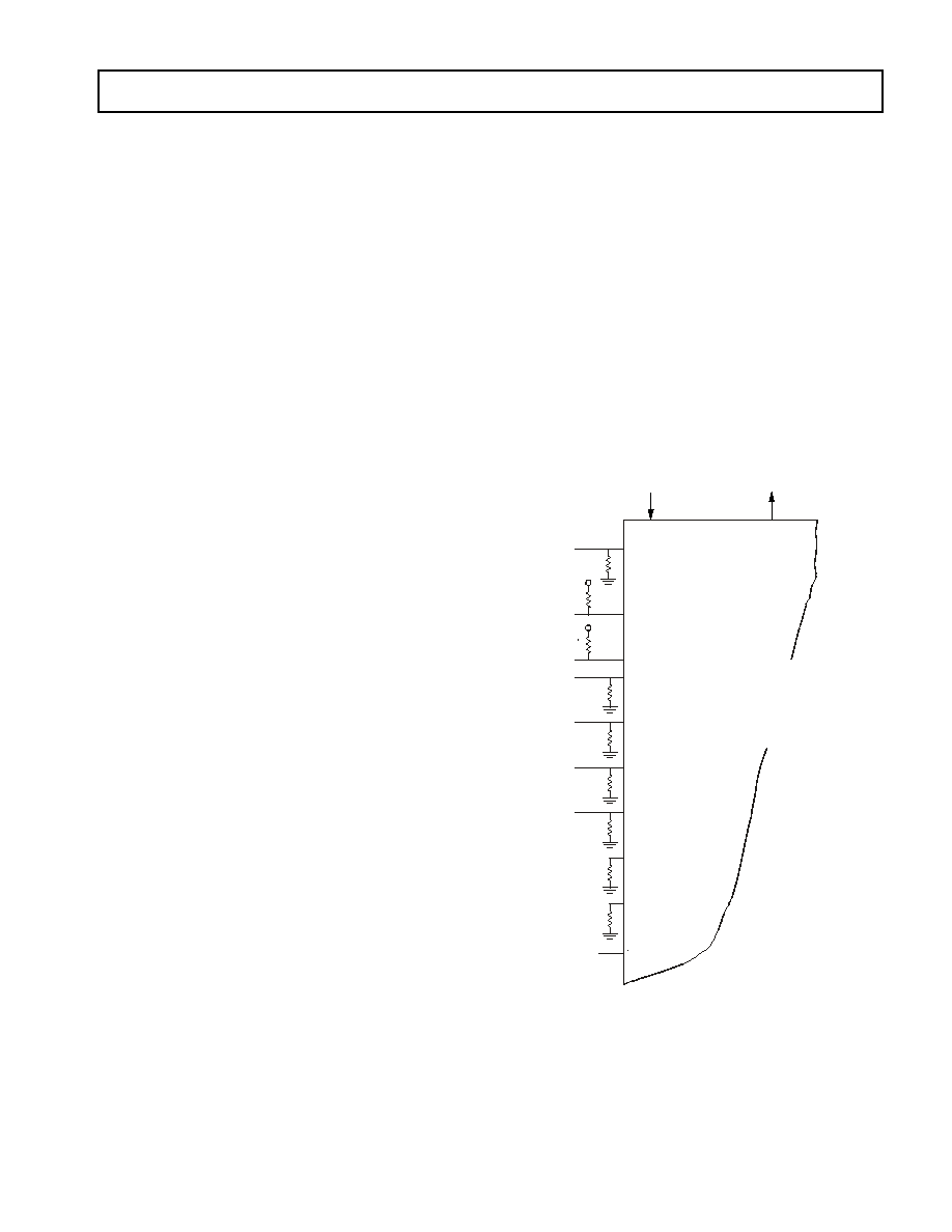
Figure 7. Clock Ratio Example
CLKIN
CLKOUT
ADSP-BF535
MSEL5 (PF5)
MSEL4 (PF4)
MSEL3 (PF3)
MSEL2 (PF2)
MSEL1 (PF1)
MSEL0 (PF0)
RESET
MSEL6 (PF6)
DF (PF7)
V
DD
BYPASS
RESET SOURCE
THE PULL-UP/PULL-DOWN
RESISTORS ON THE MSEL,
DF, AND BYPASS PINS SELECT
THE CORE CLOCK RATIO.
HERE, THE SELECTION (6:1)
AND 25MHz INPUT CLOCK
PRODUCE A 150MHz CORE CLOCK.
BLACKFIN PROCESSOR
V
DD

ADSP-BF535
14
REV. A
SSEL fields define a divide ratio between the core clock (CCLK)
and the system clock.
Table 5
illustrates the system clock ratios.
The system clock is supplied to the CLKOUT_SCLK0 pin.
The maximum frequency of the system clock is f
SCLK
. Note that
the divisor ratio must be chosen to limit the system clock
frequency to its maximum of f
SCLK
. The reset value of the
SSEL10 is determined by sampling the SSEL1 and SSEL0 pins
during reset. The SSEL value can be changed dynamically by
writing the appropriate values to the PLL control register
(PLL_CTL), as described in the ADSP-BF535 Blackfin Processor
Hardware Reference.
Booting Modes
The ADSP-BF535 has three mechanisms (listed in
Table 6
) for
automatically loading internal L2 memory after a reset. A fourth
mode is provided to execute from external memory, bypassing
the boot sequence.
The BMODE pins of the reset configuration register, sampled
during power-on resets and software initiated resets, implement
these modes:
·
Execute from 16-bit external memory--Execution
starts from address 0x2000000 with 16-bit packing.
The boot ROM is bypassed in this mode.
·
Boot from 8-bit external flash memory--The 8-bit flash
boot routine located in boot ROM memory space is set
up using asynchronous Memory Bank 0. All configura-
tion settings are set for the slowest device possible
(3-cycle hold time; 15-cycle R/W access times; 4-cycle
setup).
·
Boot from SPI serial EEPROM (8-bit addressable)--
The SPI0 uses PF10 output pin to select a single SPI
EPROM device, submits a read command at address
0x00, and begins clocking data into the beginning of L2
memory. An 8-bit addressable SPI compatible EPROM
must be used.
·
Boot from SPI serial EEPROM (16-bit addressable)--
The SPI0 uses PF10 output pin to select a single SPI
EPROM device, submits a read command at address
0x0000, and begins clocking data into the beginning of
L2 memory. A 16-bit addressable SPI compatible
EPROM must be used.
For each of the boot modes described above, a four-byte value is
first read from the memory device. This value is used to specify
a subsequent number of bytes to be read into the beginning of
L2 memory space. Once each of the loads is complete, the
processor jumps to the beginning of L2 space and begins
execution.
In addition, the reset configuration register can be set by appli-
cation code to bypass the normal boot sequence during a software
reset. For this case, the processor jumps directly to the beginning
of L2 memory space.
To augment the boot modes, a secondary software loader is
provided that adds additional booting mechanisms. This
secondary loader provides the capability to boot from PCI, 16-bit
flash memory, fast flash, variable baud rate, and so on.
Instruction Set Description
The Blackfin processor family assembly language instruction set
employs an algebraic syntax designed for ease of coding and read-
ability. The instructions have been specifically tuned to provide
a flexible, densely encoded instruction set that compiles to a very
small final memory size. The instruction set also provides fully
featured multifunction instructions that allow the programmer
to use many of the processor core resources in a single instruction.
Coupled with many features more often seen on microcontrol-
lers, this instruction set is very efficient when compiling C and
C++ source code. In addition, the architecture supports both a
user (algorithm/application code) and a supervisor (O/S kernel,
device drivers, debuggers, ISRs) mode of operations, allowing
multiple levels of access to core processor resources.
The assembly language, which takes advantage of the processor's
unique architecture, offers the following advantages:
·
Seamlessly integrated DSP/CPU features are optimized
for both 8-bit and 16-bit operations.
·
A super pipelined multi issue load/store modified Harvard
architecture, which supports two 16-bit MAC or four 8-
bit ALU + two load/store + two pointer updates per cycle.
·
All registers, I/O, and memory are mapped into a unified
4 Gbyte memory space providing a simplified program-
ming model.
Table 5. System Clock Ratios
Signal
Name
Divider
Ratio
Example Frequency
Ratios (MHz)
SSEL1 0 CCLK/SCLK
CCLK
SCLK
00
2:1
266
133
01
2.5:1
275
110
10
3:1
300
100
11
4:1
300
75
Table 6. Booting Modes
BMODE20
Description
000
Execute from 16-bit external memory
(Bypass Boot ROM)
001
Boot from 8-bit flash
010
Boot from SPI0 serial ROM
(8-bit address range)
011
Boot from SPI0 serial ROM
(16-bit address range)
100 111
Reserved

15
REV. A
ADSP-BF535
·
Microcontroller features, such as arbitrary bit and bit-
field manipulation, insertion, and extraction; integer
operations on 8-, 16-, and 32-bit data-types; and separate
user and kernel stack pointers.
·
Code density enhancements, which include intermixing
of 16- and 32-bit instructions (no mode switching, no
code segregation). Frequently used instructions are
encoded as 16-bits.
Development Tools
The ADSP-BF535 Blackfin processor is supported with a
complete set of software and hardware development tools,
including Analog Devices emulators and the VisualDSP++TM
development environment. The same emulator hardware that
supports other Analog Devices JTAG processors, also fully
emulates the ADSP-BF535 Blackfin processor.
The VisualDSP++ project management environment lets pro-
grammers develop and debug an application. This environment
includes an easy to use assembler (which is based on an algebraic
syntax), an archiver (librarian/library builder), a linker, a loader,
a cycle-accurate instruction-level simulator, a C/C++ compiler,
and a C/C++ run-time library that includes DSP and mathemat-
ical functions. A key point for these tools is C/C++ code
efficiency. The compiler has been developed for efficient transla-
tion of C/C++ code to Blackfin processor assembly. The Blackfin
processor has architectural features that improve the efficiency of
compiled C/C++ code.
The VisualDSP++ debugger has a number of important features.
Data visualization is enhanced by a plotting package that offers
a significant level of flexibility. This graphical representation of
user data enables the programmer to quickly determine the per-
formance of an algorithm. As algorithms grow in complexity, this
capability can have increasing significance on the designer's
development schedule, increasing productivity. Statistical
profiling enables the programmer to nonintrusively poll the
processor as it is running the program. This feature, unique to
VisualDSP++, enables the software developer to passively gather
important code execution metrics without interrupting the real-
time characteristics of the program. Essentially, the developer can
identify bottlenecks in software quickly and efficiently. By using
the profiler, the programmer can focus on those areas in the
program that impact performance and take corrective action.
Debugging both C/C++ and assembly programs with the
VisualDSP++ debugger, programmers can:
·
View mixed C/C++ and assembly code (interleaved
source and object information)
·
Insert breakpoints
·
Set conditional breakpoints on registers, memory, and
stacks
·
Trace instruction execution
·
View the internal pipeline to further optimize peripherals
·
Perform linear or statistical profiling of program
execution
·
Fill, dump, and graphically plot the contents of memory
·
Perform source level debugging
·
Create custom debugger windows
The VisualDSP++ IDDE lets programmers define and manage
software development. Its dialog boxes and property pages let
programmers configure and manage all development tools,
including color syntax highlighting in the VisualDSP++ editor.
These capabilities permit programmers to:
·
Control how the development tools process inputs and
generate outputs
·
Maintain a one-to-one correspondence with the tool's
command line switches
The VisualDSP++ Kernel (VDK) incorporates scheduling and
resource management tailored specifically to address the memory
and timing constraints of embedded, real-time programming.
These capabilities enable engineers to develop code more effec-
tively, eliminating the need to start from the very beginning, when
developing new application code. The VDK features include
threads, critical and unscheduled regions, semaphores, events,
and device flags. The VDK also supports priority-based, preemp-
tive, cooperative, and time-sliced scheduling approaches. In
addition, the VDK was designed to be scalable. If the application
does not use a specific feature, the support code for that feature
is excluded from the target system.
Because the VDK is a library, a developer can decide whether to
use it or not. The VDK is integrated into the VisualDSP++ devel-
opment environment, but can also be used via standard
command line tools. When the VDK is used, the development
environment assists the developer with many error-prone tasks
and assists in managing system resources, automating the gener-
ation of various VDK based objects, and visualizing the system
state, when debugging an application that uses the VDK.
VCSE is Analog Devices technology for creating, using, and
reusing software components (independent modules of substan-
tial functionality) to quickly and reliably assemble software
applications. Download components from the Web and drop
them into the application. Publish component archives from
within VisualDSP++. VCSE supports component implementa-
tion in C/C++ or assembly language.
Use the Expert Linker to visually manipulate the placement of
code and data on the embedded system. View memory utilization
in a color-coded graphical form, easily move code and data to
different areas of the processor or external memory with the drag
of the mouse, examine run-time stack and heap usage. The
Expert Linker is fully compatible with existing Linker Definition
File (LDF), allowing the developer to move between the
graphical and textual environments.
Analog Devices emulators use the IEEE 1149.1 JTAG test access
port of the ADSP-BF535 Blackfin processor to monitor and
control the target board processor during emulation. The
emulator provides full speed emulation, allowing inspection and
modification of memory, registers, and processor stacks. Nonin-
trusively in-circuit emulation is assured by the use of the
processor's JTAG interface--the emulator does not affect target
system loading or timing.
VisualDSP++ is a trademark of Analog Devices, Inc.

ADSP-BF535
16
REV. A
In addition to the software and hardware development tools
available from Analog Devices, third parties provide a wide range
of tools supporting the Blackfin processor family. Third Party
software tools include DSP libraries, real-time operating systems,
and block diagram design tools.
EZ-KIT Lite
TM
for ADSP-BF535 Blackfin Processor
The EZ-KIT Lite provides developers with a cost-effective
method for initial evaluation of the ADSP-BF535 Blackfin pro-
cessor. The EZ-KIT Lite includes a desktop evaluation board
and fundamental debugging software to facilitate architecture
evaluations via a PC hosted toolset. With the EZ-KIT Lite, users
can learn more about Analog Devices hardware and software
development tools and prototype applications. The EZ-KIT Lite
includes an evaluation suite of the VisualDSP++ development
environment with C/C++ compiler, assembler, and linker. The
VisualDSP++ software included with the kit is limited in program
memory size and limited to use with the EZ-KIT Lite product.
Designing an Emulator Compatible
Processor Board (Target)
The Analog Devices family of emulators are tools that every
system developer needs to test and debug hardware and software
systems. Analog Devices has supplied an IEEE 1149.1 JTAG Test
Access Port (TAP) on the ADSP-BF535 Blackfin processor. The
emulator uses the TAP to access the internal features of the pro-
cessor, allowing the developer to load code, set breakpoints,
observe variables, observe memory, and examine registers. The
processor must be halted to send data and commands, but once
an operation has been completed by the emulator, the processor
system is set running at full speed with no impact on system
timing.
To use these emulators, the target's design must include a header
that connects the processor's JTAG port to the emulator.
For details on target board design issues including single
processor connections, multiprocessor scan chains, signal buff-
ering, signal termination, and emulator pod logic, see the EE-68:
Analog Devices
JTAG Emulation Technical Reference on the Analog
Devices website (www.analog.com)--use site search on
"EE-68". This document is updated regularly to keep pace with
improvements to emulator support.
Additional Information
This data sheet provides a general overview of the ADSP-BF535
Blackfin processor architecture and functionality. For detailed
information on the Blackfin processor family core architecture
and instruction set, refer to the ADSP-BF535 Blackfin Processor
Hardware Reference and the Blackfin Processor Instruction Set
Reference.
EZ-KIT Lite is a trademark of Analog Devices, Inc.

17
REV. A
ADSP-BF535
PIN DESCRIPTIONS
ADSP-BF535 Blackfin processor pin definitions are listed in
Table 7
. The following pins are asynchronous: ARDY, PF150,
USB_CLK, NMI,
TRST, RESET, PCI_CLK, XTALI,
XTALO.
Table 7. Pin Descriptions
Pin
Type
Function
ADDR25 2
O/T
External address bus.
DATA31 0
I/O/T External data bus. (Pin has a logic-level hold circuit that prevents the input from floating
internally.)
ABE30/SDQM30
O/T
Asynchronous memory byte enables SDRAM data masks.
AMS30
O/T
Chip selects for asynchronous memories.
ARDY
1
I
Acknowledge signal for asynchronous memories.
AOE
O/T
Memory output enable for asynchronous memories.
ARE
O
Read enable for asynchronous memories.
AWE
O
Write enable for asynchronous memories.
CLKOUT/SCLK1
O
SDRAM clock output pin. Same frequency and timing as SCLK0. Provided to reduce
capacitance loading on SCLK0. Connect to SDRAM's CK pin.
SCLK0
O
SDRAM clock output pin 0. Switches at system clock frequency. Connect to the
SDRAM's CK pin.
SCKE
O/T
SDRAM clock enable pin. Connect to SDRAM's CKE pin.
SA10
O/T
SDRAM A10 pin. SDRAM interface uses this pin to retain control of the SDRAM device
during host bus requests. Connect to SDRAM's A10 pin.
SRAS
O/T
SDRAM row address strobe pin. Connect to SDRAM's RAS pin.
SCAS
O/T
SDRAM column address select pin. Connect to SDRAM's CAS pin.
SWE
O/T
SDRAM write enable pin. Connect to SDRAM's WE or W buffer pin.
SMS30
O/T
Memory select pin of external memory bank configured for SDRAM. Connect to
SDRAM's chip select pin.
TMR0
I/O/T Timer 0 pin. Functions as an output pin in PWMOUT mode and as an input pin in
WIDTH_CNT and EXT_CLK modes.
TMR1
I/O/T Timer 1 pin. Functions as an output pin in PWMOUT mode and as an input pin in
WIDTH_CNT and EXT_CLK modes.
TMR2
I/O/T Timer 2 pin. Functions as an output pin in PWMOUT mode and as an input pin in
WIDTH_CNT and EXT_CLK modes.
PF15/
SPI1SEL7
I/O/T Programmable flag pin. SPI output select pin.
PF14/
SPI0SEL7
I/O/T Programmable flag pin. SPI output select pin.
PF13/
SPI1SEL6
I/O/T Programmable flag pin. SPI output select pin.
PF12/
SPI0SEL6
I/O/T Programmable flag pin. SPI output select pin.
PF11/
SPI1SEL5
I/O/T Programmable flag pin. SPI output select pin.
PF10/
SPI0SEL5
I/O/T Programmable flag pin. SPI output select pin (used during SPI boot).
PF9/
SPI1SEL4/SSEL1
I/O
Programmable flag pin. SPI output select pin. Sampled during reset to determine core
clock to system clock ratio.
PF8/
SPI0SEL4/SSEL0
I/O
Programmable flag pin. SPI output select pin. Sampled during reset to determine core
clock to system clock ratio.
PF7/
SPI1SEL3/DF
I/O
Programmable flag pin. SPI output select pin. Sensed for configuration state during
hardware reset, used to configure the PLL. DF = 1 is for high frequency clock and divides
the input clock by 2. DF = 0 passes input clock directly to PLL phase detector.
PF6/
SPI0SEL3/MSEL6 I/O
Programmable flag pin. SPI output select pin. Sensed for configuration state during
hardware reset, used to configure the PLL. Selects CK to CLKIN ratio.
PF5/
SPI1SEL2/MSEL5 I/O
Programmable flag pin. SPI output select pin. Sensed for configuration state during
hardware reset, used to configure the PLL. Selects CK to CLKIN ratio.
Type column symbols: G = Ground, I = Input, O = Output, P = Power supply, T = Three-state

ADSP-BF535
18
REV. A
PF4/
SPI0SEL2/MSEL4 I/O
Programmable flag pin. SPI output select pin. Sensed for configuration state during
hardware reset, used to configure the PLL. Selects CK to CLKIN ratio.
PF3/
SPI1SEL1/MSEL3 I/O
Programmable flag pin. SPI output select pin. Sensed for configuration state during
hardware reset, used to configure the PLL. Selects CK to CLKIN ratio.
PF2/
SPI0SEL1/MSEL2 I/O
Programmable flag pin. SPI output select pin. Sensed for configuration state during
hardware reset, used to configure the PLL. Selects CK to CLKIN ratio.
PF1/
SPISS1/MSEL1
I/O
Programmable flag pin. SPI slave select input pin. Sensed for configuration state during
hardware reset, used to configure the PLL. Selects CK to CLKIN ratio.
PF0/
SPISS0/MSEL0
I/O
Programmable flag pin. SPI slave select input pin. Sensed for configuration state during
hardware reset, used to configure the PLL. Selects CK to CLKIN ratio.
RSCLK0
I/O/T Receive serial clock for SPORT0.
RFS0
I/O/T Receive frame synchronization for SPORT0.
DR0
I
Serial data receive for SPORT0.
TSCLK0
I/O/T Transmit serial clock for SPORT0.
TFS0
I/O/T Transmit frame synchronization for SPORT0.
DT0
O
Serial data transmit for SPORT0.
RSCLK1
I/O/T Receive serial clock for SPORT1.
RFS1
I/O/T Receive frame synchronization for SPORT1.
DR1
I
Serial data receive for SPORT1.
TSCLK1
I/O/T Transmit serial clock for SPORT1.
TFS1
I/O/T Transmit frame synchronization for SPORT1.
DT1
O
Serial data transmit for SPORT1.
MOSI0
I/O
Master out slave in pin for SPI0. Supplies the output data from the master device and
receives the input data to a slave device.
MISO0
I/O
Master in slave out pin for SPI0. Supplies the output data from the slave device and
receives the input data to the master device.
SCK0
I/O
Clock line for SPI0. Master device output clock signal. Slave device input clock signal.
MOSI1
I/O
Master out slave in pin for SPI1. Supplies the output data from the master device and
receives the input data to a slave device.
MISO1
I/O
Master in slave out pin for SPI1. Supplies the output data from the slave device and
receives the input data to the master device.
SCK1
I/O
Clock line for SPI1. Master device output clock signal. Slave device input clock signal.
RX0
I
UART0 receive pin.
TX0
O
UART0 transmit pin.
RX1
I
UART1 receive pin.
TX1
O
UART1 transmit pin.
USB_CLK
I
USB clock.
XVER_DATA
I
Single ended receive data output from USB transceiver to the USBD module.
DPLS
I
Differential D+ receive data output from the USB transceiver to the UBD module.
DMNS
I
Differential D- receive data output from the USB transceiver to the USBD module.
TXDPLS
O
Transmitted D+ from the USBD module to the USB transceiver.
TXDMNS
O
Transmitted D- from the USBD module to the USB transceiver.
TXEN
O
Transmit enable from the USBD module to the USB transceiver.
SUSPEND
O
Suspend mode enable output from the USBD module to the USB transceiver.
NMI
I
Non-maskable interrupt.
TCK
I
JTAG clock.
TDO
O/T
JTAG serial data out.
TDI
I
JTAG serial data in.
TMS
I
Test mode select.
Table 7. Pin Descriptions (continued)
Pin
Type
Function
Type column symbols: G = Ground, I = Input, O = Output, P = Power supply, T = Three-state

19
REV. A
ADSP-BF535
TRST
I
JTAG reset.
RESET
I
When this pin is asserted to logic zero level for at least 10 CLKIN cycles, a hardware reset
is initiated. The minimum pulse width for power-on reset is 40 µs.
CLKIN1
I
Clock in.
BYPASS
I
Dedicated mode pin. May be permanently strapped to V
DD
or V
SS
. Bypasses the on-chip
PLL.
DEEPSLEEP
O
Denotes that the Blackfin processor core is in Deep Sleep mode.
BMODE2 0
I
Dedicated mode pin. May be permanently strapped to V
DD
or V
SS
. Configures the boot
mode that is employed following hardware reset or software reset.
PCI_AD31 0
I/O/T PCI address and data bus.
PCI_CBE30
I/O/T PCI byte enables.
PCI_FRAME
I/O/T PCI frame signal. Used by PCI initiators for signalling the beginning and end of a PCI
transaction.
PCI_IRDY
I/O/T PCI initiator ready signal.
PCI_TRDY
I/O/T PCI target ready signal.
PCI_DEVSEL
I/O/T PCI device select signal. Asserted by targets of PCI transactions to claim the transaction.
PCI_STOP
I/O/T PCI stop signal.
PCI_PERR
I/O/T PCI parity error signal.
PCI_PAR
I/O/T PCI parity signal.
PCI_REQ
O
PCI request signal. Used for requesting the use of the PCI bus.
PCI_SERR
I/O/T PCI system error signal. Requires a pull-up on the system board.
PCI_RST
I/O/T PCI reset signal.
PCI_GNT
I
PCI grant signal. Used for granting access to the PCI bus.
PCI_IDSEL
I
PCI initialization device select signal. Individual device selects for targets of PCI config-
uration transactions.
PCI_LOCK
I
PCI lock signal. Used to lock a target or the entire PCI bus for use by the master that
asserts the lock.
PCI_CLK
I
PCI clock.
PCI_INTA
I/O/T PCI interrupt A line on PCI bus. Asserted by the ADSP-BF535 Blackfin processor as a
device-to-signal an interrupt to the system processor. Monitored by the ADSP-BF535
when acting as the system processor.
PCI_INTB
I
PCI interrupt B line. Monitored by ADSP-BF535 Blackfin processor when acting as the
system processor.
PCI_INTC
I
PCI interrupt C line. Monitored by the ADSP-BF535 Blackfin processor when acting as
the system processor.
PCI_INTD
I
PCI interrupt D line. Monitored by the ADSP-BF535 Blackfin processor when acting as
the system processor.
XTAL1
I
Real-Time Clock oscillator input.
XTAL0
O
Real-Time Clock oscillator output.
EMU
O
Emulator acknowledge, open drain. Must be connected to the ADSP-BF535 Blackfin
processor emulator target board connector only.
V
DDPLL
P
PLL power supply (1.5 V nominal).
V
DDRTC
P
Real-Time Clock power supply (3.3 V nominal).
V
DDEXT
P
I/O (except PCI) power supply (3.3 V nominal).
V
DDPCIEXT
P
PCI I/O power supply (3.3 V nominal).
V
DDINT
P
Internal power supply (1.5 V nominal).
GND
G
Power supply return.
Table 7. Pin Descriptions (continued)
Pin
Type
Function
Type column symbols: G = Ground, I = Input, O = Output, P = Power supply, T = Three-state

ADSP-BF535
20
REV. A
Unused Pins
Table 8
shows recommendations for tying off unused pins. All
pins that are not listed in the table should be left floating.
Table 8. Recommendations for Tying Off Unused Pins
Pin Tie
Off
ARDY
V
DDEXT
BMODE2 0
V
DDEXT
or GND
BYPASS
V
DDEXT
or GND
DMNS
GND
DPLS
GND
DR0
V
DDEXT
or GND
DR1
V
DDEXT
or GND
NMI
GND
PCI_AD310
V
DDEXT
PCI_CB30
V
DDEXT
PCI_CLK
GND
PCI_DEVSEL
V
DDEXT
PCI_FRAME
V
DDEXT
PCI_GNT
V
DDEXT
PCI_IDSEL
GND
PCI_INTA
V
DDEXT
PCI_INTB
V
DDEXT
PCI_INTC
V
DDEXT
PCI_INTD
V
DDEXT
PCI_IRDY
V
DDEXT
PCI_LOCK
V
DDEXT
PCI_PAR
V
DDEXT
PCI_PERR
V
DDEXT
PCI_RST
V
DDEXT
PCI_STOP
V
DDEXT
PCI_SERR
V
DDEXT
PCI_TRDY
V
DDEXT
PF0/
SPISS0/MSEL0
V
DDEXT
or GND (10 k
pull-up/pull-down required)
PF1/
SPISS1/MSEL1
V
DDEXT
or GND (10 k
pull-up/pull-down required)
PF2/
SPI0SEL1/MSEL2 V
DDEXT
or GND (10 k
pull-up/pull-down required)
PF3/
SPI1SEL1/MSEL3 V
DDEXT
or GND (10 k
pull-up/pull-down required)
PF4/
SPI0SEL2/MSEL4 V
DDEXT
or GND (10 k
pull-up/pull-down required)
PF5/
SPI1SEL2/MSEL5 V
DDEXT
or GND (10 k
pull-up/pull-down required)
PF6/
SPI0SEL3/MSEL6 V
DDEXT
or GND (10 k
pull-up/pull-down required)
PF7/
SPI1SEL3/DF
V
DDEXT
or GND (10 k
pull-up/pull-down required)
PF8/
SPI0SEL4/SSEL0
V
DDEXT
or GND (10 k
pull-up/pull-down required)
PF9/
SPI1SEL4/SSEL1
V
DDEXT
or GND (10 k
pull-up/pull-down required)
RX0
V
DDEXT
or GND
RX1
V
DDEXT
or GND
TCK
V
DDEXT
TDI
V
DDEXT
TMS
V
DDEXT
TRST
GND
USB_CLK
GND
V
DDPCIEXT
V
DDEXT
V
DDRTC
V
DDEXT
XTAL1
V
DDEXT
or GND
XVER_DATA
GND

21
REV. A
ADSP-BF535
SPECIFICATIONS
RECOMMENDED OPERATING CONDITIONS
Parameter Min
Nominal
Max
Unit
V
DDINT
Internal (Core) Supply Voltage
1
1
There is no requirement for sequencing of the voltage supplies on powerup, however, the supply regulators must be able to provide the required current
I
DDRESET
at all times. See
Table 26
.
ADSP-BF535PKB-350
ADSP-BF535PKB-300
ADSP-BF535PBB-300
ADSP-BF535PBB-200
0.95
1.6
1.65
V
0.95
1.5
1.575
V
0.95
1.5
1.575
V
0.95
1.5
1.575
V
V
DDEXT
External (I/O) Supply Voltage
1
3.15
3.3
3.45
V
V
DDPLL
PLL Power Supply Voltage
1
1.425
1.5
1.575
V
V
DDRTC
Real-Time Clock Power Supply Voltage
1
2.60
3.3
3.45
V
V
DDPCIEXT
PCI I/O Power Supply Voltage
1
3.15
3.3
3.45
V
V
IH
High Level Input Voltage
2
, @ V
DDEXT
= max
2
Applies to input and bidirectional pins, except PCI and USB_CLK.
2.2
V
DDEXT
+ 0.5
V
V
IL
Low Level Input Voltage
2
, @ V
DDEXT
= min
0.3
+ 0.6
V
V
IHUSBCLK
High Level Input Voltage
3
, @ V
DDEXT
= max
3
Applies to USB_CLK.
2.4
V
DDEXT
+ 0.5
V
V
IHPCI
High Level Input Voltage
4
, @ V
DDPCIEXT
= max
4
Applies to PCI input and bidirectional pins: PCI_AD31 0,
PCI_CBE30, PCI_FRAME, PCI_IRDY, PCI_TRDY, PCI_DEVSEL, PCI_STOP,
PCI_PERR, PCI_PAR, PCI_SERR, PCI_RST, PCI_GNT, PCI_IDSEL, PCI_LOCK, PCI_CLK, PCI_INTA, PCI_INTB, PCI_INTC, PCI_INTD.
0.5 V
DDPCIEXT
V
DDPCIEXT
+ 0.5
V
V
ILPCI
Low Level Input Voltage
4
, @ V
DDPCIINT
= min
0.5
+ 0.3 V
DDPCIEXT
V
T
A
Ambient Operating Temperature
ºC
Commercial
0
70
ºC
Industrial
40
+ 85
ºC
Specifications subject to change without notice.
ELECTRICAL CHARACTERISTICS
Parameter
Test Conditions
Min
Max
Unit
V
OH
High Level Output Voltage
1
1
Applies to output and bidirectional pins, except PCI.
@ V
DDEXT
= min, I
OH
= 0.5 mA
2.4
V
V
OL
Low Level Output Voltage
1
@ V
DDEXT
= max, I
OL
= 2.0 mA
0.4
V
V
OHPCI
PCI High Level Output Voltage
2
2
Applies to PCI output and bidirectional pins: PCI_AD310,
PCI_CBE30, PCI_FRAME, PCI_IRDY, PCI_TRDY, PCI_DEVSEL, PCI_STOP,
PCI_PERR, PCI_PAR, PCI_REQ, PCI_SERR, PCI_RST, PCI_INTA.
@ V
DDPCIEXT
= min, I
OH
= 0.5 mA 0.9 V
DDPCIEXT
V
V
OLPCI
PCI Low Level Output Voltage
2
@ V
DDPCIEXT
= max, I
OL
= 2.0 mA
0.1 V
DDPCIEXT
V
I
IH
High Level Input Current
3
3
Applies to input pins.
@ V
DDEXT
= max, V
IN
= V
DD
max
10
µA
I
IL
Low Level Input Current
3
@ V
DDEXT
= max, V
IN
= 0 V
10
µA
I
OZH
Three-State Leakage Current
4
4
Applies to three-statable pins.
@ V
DDEXT
= max, V
IN
= V
DD
max
10
µA
I
OZL
Three-State Leakage Current
4
@ V
DDEXT
= max, V
IN
= 0 V
10
µA
C
IN
Input Capacitance
5, 6
5
Applies to all signal pins.
6
Guaranteed but not tested.
f
IN
= 1 MHz,
T
A
= 25°C, V
IN
= 2.5 V
5
pF
Specifications subject to change without notice.

ADSP-BF535
22
REV. A
ABSOLUTE MAXIMUM RATINGS
ESD SENSITIVITY
Internal (Core) Supply Voltage (V
DDINT
)
1
. 0.3 V to + 1.65 V
External (I/O) Supply Voltage (V
DDEXT
)
1
. . . 0.3 V to + 4.0 V
Input Voltage
1
. . . . . . . . . . . . . . . . 0.5 V to V
DDEXT
+ 0.5 V
Output Voltage Swing
1
. . . . . . . . . 0.5 V to V
DDEXT
+ 0.5 V
Load Capacitance
1, 2
. . . . . . . . . . . . . . . . . . . . . . . . 200 pF
Core Clock:
1
ADSP-BF535PKB-350 . . . . . . . . . . . . . . . . . 350 MHz
ADSP-BF535PKB-300 . . . . . . . . . . . . . . . . . 300 MHz
ADSP-BF535PBB-300 . . . . . . . . . . . . . . . . . 300 MHz
ADSP-BF535PBB-200 . . . . . . . . . . . . . . . . . 200 MHz
System Clock (SCLK)
1
. . . . . . . . . . . . . . . . . . . . 133 MHz
Storage Temperature Range
1
. . . . . . . . . . 65ºC to + 150ºC
1
Stresses greater than those listed above may cause permanent damage to the
device. These are stress ratings only; functional operation of the device at these
or any other conditions greater than those indicated in the operational sections
of this specification is not implied. Exposure to absolute maximum rating
conditions for extended periods may affect device reliability.
2
For proper SDRAM controller operation, the maximum load capacitance is 50 pF
for ADDR, DATA,
ABE30/SDQM30, CLKOUT/SCLK1, SCLK0, SCKE,
SA10,
SRAS, SCAS, SWE, and SMS3-0.
CAUTION
ESD (electrostatic discharge) sensitive device. Electrostatic charges as high as 4000 V
readily accumulate on the human body and test equipment and can discharge without
detection. Although the ADSP-BF535 features proprietary ESD protection circuitry,
permanent damage may occur on devices subjected to high energy electrostatic
discharges. Therefore, proper ESD precautions are recommended to avoid perfor-
mance degradation or loss of functionality.

23
REV. A
ADSP-BF535
TIMING SPECIFICATIONS
Table 9
and
Table 10
describe the timing requirements for the
ADSP-BF535 Blackfin processor clocks. Take care in selecting
MSEL and SSEL ratios so as not to exceed the maximum core
clock, system clock and Voltage Controlled Oscillator (VCO)
operating frequencies, as described in Absolute Maximum
Ratings
on Page 22
.
Table 10
describes phase-locked loop
operating conditions.
Table 9. Core Clock Requirements
Parameter
Min
Max
Unit
t
CCLK1.6
Core Cycle Period (V
DDINT
= 1.6 V 50 mV)
2.86
200
ns
t
CCLK1.5
Core Cycle Period (V
DDINT
= 1.5 V 5%)
3.33
200
ns
t
CCLK1.4
Core Cycle Period (V
DDINT
= 1.4 V 5%)
3.70
200
ns
t
CCLK1.3
Core Cycle Period (V
DDINT
= 1.3 V 5%)
4.17
200
ns
t
CCLK1.2
Core Cycle Period (V
DDINT
= 1.2 V 5%)
4.76
200
ns
t
CCLK1.1
Core Cycle Period (V
DDINT
= 1.1 V 5%)
5.56
200
ns
t
CCLK1.0
Core Cycle Period (V
DDINT
= 1.0 V 5%)
6.67
200
ns
Table 10. Phase-Locked Loop Operating Conditions
Parameter
Min
Nominal
Max
Unit
Operating Voltage
1.425
1.5
1.575
V
Jitter, Rising Edge to Rising Edge, Per Output
1
120
ps
Jitter, Rising Edge to Falling Edge, Per Output
1
60
ps
Skew, Rising Edge to Rising Edge, Any Two Outputs
1
120
ps
Voltage Controlled Oscillator (VCO) Frequency
1
40
400
MHz
V
DDPLL
Induced Jitter
1
1
ps/mV
1
Guaranteed but not tested.
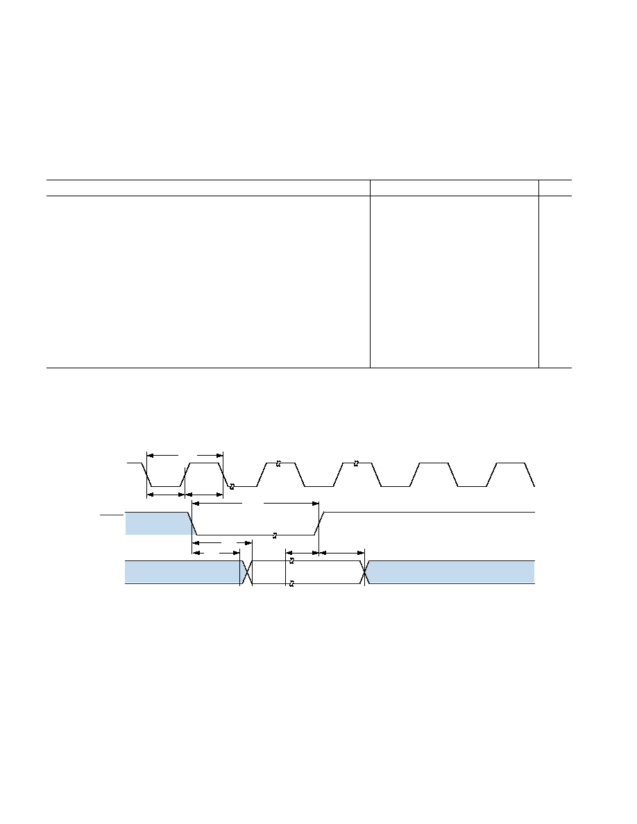
ADSP-BF535
24
REV. A
Clock and Reset Timing
Table 11
and
Figure 8
describe clock and reset operations. Per
ABSOLUTE MAXIMUM RATINGS on Page 22
, combina-
tions of CLKIN and clock multipliers must not select core and
system clocks in excess of 350/300/200 MHz and 133 MHz,
respectively.
Table 11. Clock and Reset Timing
Parameter
Min
Max
Unit
Timing Requirements
t
CKIN
CLKIN Period
25.0
100.0
ns
t
CKINL
CLKIN Low Pulse
1
10.0
ns
t
CKINH
CLKIN High Pulse
1
10.0
ns
t
WRST
RESET Asserted Pulse Width Low
2
11
t
CKIN
ns
t
MSD
Delay from
RESET Asserted to MSELx, SSELx, BYPASS,
and DF Valid
3
15.0
ns
t
MSS
MSELx/SSELx/DF/BYPASS Stable Setup Before
RESET
Deasserted
4
2
t
CKIN
ns
t
MSH
MSELx/SSELx/DF/BYPASS Stable Hold After
RESET
Deasserted
2
t
CKIN
ns
Switching Characteristics
t
PFD
Flag Output Disable Time After
RESET Asserted
15.0
ns
1
Applies to Bypass mode and Non-bypass mode.
2
Applies after power-up sequence is complete. At power-up, the processor's internal phase-locked loop requires no more than 2000 CLKIN cycles, while
RESET is asserted, assuming stable power supplies and CLKIN (not including start-up time of external clock oscillator).
3
SSELx, MSELx and DF values can change from this point, but the values must be valid.
4
SSELx, MSELx and DF values must be held from this time, until the hold time expires.
Figure 8. Clock and Reset Timing
SSEL10
MSEL60
BYPASS
DF
RESET
CLKIN
t
W R S T
t
C K IN H
t
C K IN
t
C K IN L
t
M S H
t
P F D
t
M S D
t
M S S
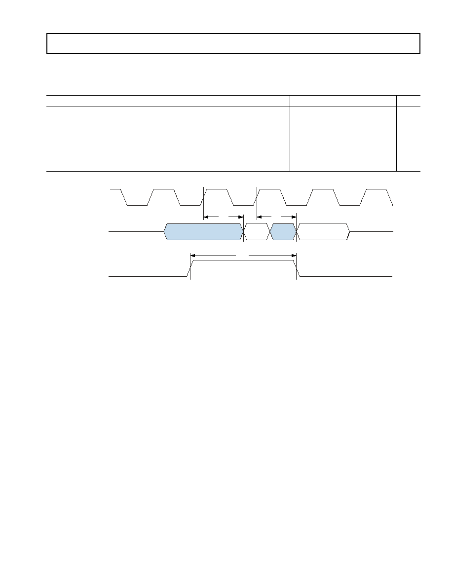
25
REV. A
ADSP-BF535
Programmable Flags Cycle Timing
Table 12
and
Figure 9
describe programmable flag operations.
Table 12. Programmable Flags Cycle Timing
Parameter
Min
Max
Unit
Timing Requirements
t
HFIES
Edge Sensitive Flag Input Hold is Asynchronous
3.0
ns
t
HFILS
Level Sensitive Flag Input Hold
t
SCLK
+3
ns
Switching Characteristics
t
DFO
Flag Output Delay with Respect to SCLK
6.0
ns
t
HFO
Flag Output Hold After SCLK High
6.0
ns
Figure 9. Programmable Flags Cycle Timing
FLAG INPUT
PF (INPUT)
t
HFIxS
PF (OUTPUT)
SCLK
FLAG
OUTPUT
t
DFO
t
HFO

ADSP-BF535
26
REV. A
Timer PWM_OUT Cycle Timing
Table 13
and
Figure 10
describe timer expired operations. The
input signal is asynchronous in "width capture mode" and has
an absolute maximum input frequency of f
SCLK
2.
Table 13. Timer PWM_OUT Cycle Timing
Parameter
Min
Max
Unit
Switching Characteristics
t
HTO
Timer Pulse Width Output
1
7.5
(2
32
1) cycles
ns
1
The minimum time for t
HTO
is one cycle, and the maximum time for t
HTO
equals (2
32
1) cycles.
Figure 10. Timer PWM_OUT Cycle Timing
SCLK
PWM_OUT
t
HTO
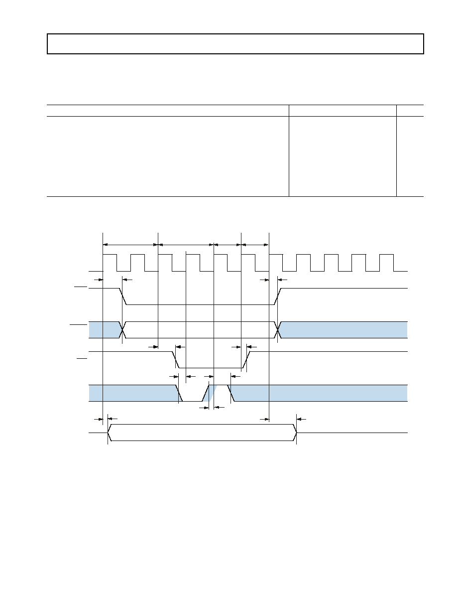
27
REV. A
ADSP-BF535
Asynchronous Memory Write Cycle Timing
Table 14
and
Figure 11
describe Asynchronous Memory Write
Cycle timing.
Table 14. Asynchronous Memory Write Cycle Timing
Parameter
Min
Max
Unit
Timing Requirements
t
SARDY
ARDY Setup Before CLKOUT
4.0
ns
t
HARDY
ARDY Hold After CLKOUT
1.0
ns
Switching Characteristics
t
DDAT
DATA31 0 Disable After CLKOUT
6.0
ns
t
ENDAT
DATA31 0 Enable After CLKOUT
1.0
ns
t
DO
Output Delay After CLKOUT
1
7.0
ns
t
HO
Output Hold After CLKOUT
1
0.8
ns
1
Output pins include
AMS30, ABE30, ADDR252, DATA310, AOE, AWE.
Figure 11. Asynchronous Memory Write Cycle Timing
t
DO
t
ENDAT
CLKOUT
AMSx
ABE30
BE, ADDRESS
t
HO
WRITE DATA
t
DDAT
DATA310
AWE
t
SARDY
t
HARDY
SETUP
2 CYCLES
PROGRAMMED WRITE
ACCESS 2 CYCLES
ACCESS
EXTENDED
1 CYCLE
HOLD
1 CYCLE
ARDY
ADDR252
t
HO
t
SARDY
t
DO

ADSP-BF535
28
REV. A
Asynchronous Memory Read Cycle Timing
Table 15
and
Figure 12
describe Asynchronous Memory Read
Cycle timing.
Table 15. Asynchronous Memory Read Cycle Timing
Parameter
Min
Max
Unit
Timing Requirements
t
SDAT
DATA31 0 Setup Before CLKOUT
2.1
ns
t
HDAT
DATA31 0 Hold After CLKOUT
2.6
ns
t
SARDY
ARDY Setup Before CLKOUT
4.0
ns
t
HARDY
ARDY Hold After CLKOUT
1.0
ns
Switching Characteristics
t
DO
Output Delay After CLKOUT
1
7.0
ns
t
HO
Output Hold After CLKOUT
1
0.8
ns
1
Output pins include
AMS30, ABE30, ADDR252, AOE, ARE.
Figure 12. Asynchronous Memory Read Cycle Timing
t
DO
t
SDAT
CLKOUT
AMSx
ABE30
t
HO
BE, ADDRESS
READ
t
HDAT
DATA310
AOE
t
DO
t
SARDY
t
HARDY
ACCESS EXTENDED
3 CYCLES
HOLD
1 CYCLE
ARE
t
HARDY
ARDY
ADDR252
SETUP
2 CYCLES
PROGRAMMED READ ACCESS
4 CYCLES
t
HO
t
SARDY
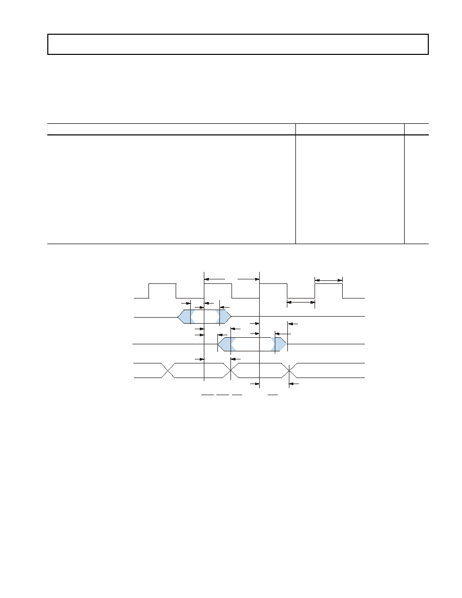
29
REV. A
ADSP-BF535
SDRAM Interface Timing
For proper SDRAM controller operation, the maximum load
capacitance is 50 pF for ADDR, DATA,
ABE30/SDQM30,
CLKOUT/SCLK1, SCLK0, SCKE, SA10,
SRAS, SCAS, SWE,
and
SMS3-0.
Table 16. SDRAM Interface Timing
Parameter
Min
Max
Unit
Timing Requirements
t
SSDAT
DATA Setup Before SCLK0/SCLK1
2.1
ns
t
HSDAT
DATA Hold After SCLK0/SCLK1
2.8
ns
Switching Characteristics
t
SCLK
SCLK0/SCLK1 Period
7.5
ns
t
SCLKH
SCLK0/SCLK1 Width High
2.5
ns
t
SCLKL
SCLK0/SCLK1 Width Low
2.5
ns
t
DCAD
Command, ADDR, Data Delay After SCLK0/SCLK1
1
6.0
ns
t
HCAD
Command, ADDR, Data Hold After SCLK0/SCLK1
1
0.8
ns
t
DSDAT
Data Disable After SCLK0/SCLK1
6.0
ns
t
ENSDAT
Data Enable After SCLK0/SCLK1
1.0
ns
1
Command pins include:
SRAS, SCAS, SWE, SDQM30, SMS, SA10, and SCKE.
Figure 13. SDRAM Interface Timing
t
HCAD
t
HCAD
t
DSDAT
t
DCAD
t
SSDAT
t
DCAD
t
ENSDAT
t
HSDAT
t
SCLKL
t
SCLKH
t
SCLK
SCLK0/
SCLK1
DATA
(IN)
DATA
(OUT)
CMND1
ADDR
(OUT)
NOTE 1: COMMAND = SRAS, SCAS, SWE, SDQM30, SMS, SA10, AND SCKE.

ADSP-BF535
30
REV. A
Serial Ports
Table 17
through
Table 22
and
Figure 14
describe Serial Port
timing.
Table 17. Serial Ports--External Clock
Parameter
Min
Max
Unit
Timing Requirements
t
SFSE
TFS/RFS Setup Before TCLK/RCLK
1
3.0
ns
t
HFSE
TFS/RFS Hold After TCLK/RCLK
1
3.0
ns
t
SDRE
Receive Data Setup Before RCLK
1
3.0
ns
t
HDRE
Receive Data Hold Before RCLK
1
3.0
ns
t
SCLKWE
TCLK/RCLK Width
(0.5
t
SCLKE
) 1
ns
t
SCLKE
TCLK/RCLK Period
2
t
SCLK
ns
1
Referenced to sample edge.
Table 18. Serial Ports--Internal Clock
Parameter
Min
Max
Unit
Timing Requirements
t
SFSI
TFS/RFS Setup Before TCLK/RCLK
1
7.0
ns
t
HFSI
TFS/RFS Hold After TCLK/RCLK
1
2.0
ns
t
SDRI
Receive Data Setup Before RCLK
1
7.0
ns
t
HDRI
Receive Data Hold Before RCLK
1
4.0
ns
1
Referenced to sample edge.
Table 19. Serial Ports--External or Internal Clock
Parameter
Min
Max
Unit
Switching Characteristics
t
DFSE
RFS Delay After RCLK (Internally Generated RFS)
1
10.0
ns
t
HOFSE
RFS Hold After RCLK (Internally Generated RFS)
1
3.0
ns
1
Referenced to drive edge.
Table 20. Serial Ports--External Clock
Parameter
Min
Max
Unit
Switching Characteristics
t
DFSE
TFS Delay After TCLK (Internally Generated TFS)
1
10.0
ns
t
HOFSE
TFS Hold After TCLK (Internally Generated TFS)
1
3.0
ns
t
DDTE
Transmit Data Delay After TCLK
1
10.0
ns
t
HDTE
Transmit Data Hold After TCLK
1
3.0
ns
1
Referenced to drive edge.
Table 21. Serial Ports--Internal Clock
Parameter
Min
Max
Unit
Switching Characteristics
t
DFSI
TFS Delay After TCLK (Internally Generated TFS)
1
6.0
ns
t
HOFSI
TFS Hold After TCLK (Internally Generated TFS)
1
0.0
ns
t
DDTI
Transmit Data Delay After TCLK
1
8.0
ns
t
HDTI
Transmit Data Hold After TCLK
1
0.0
ns
t
SCLKWI
TCLK/RCLK Width
0.5
t
SCLK
ns
1
Referenced to drive edge.
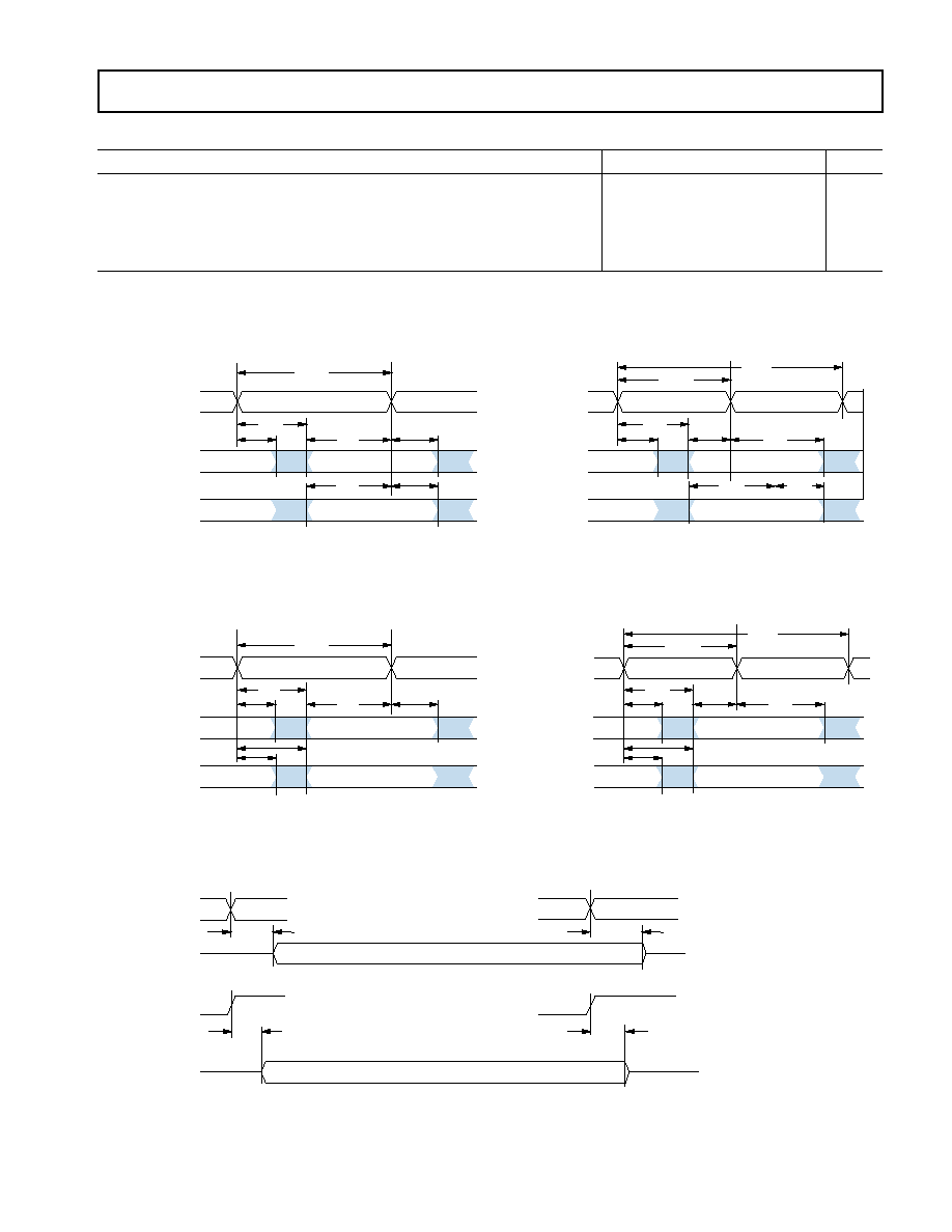
31
REV. A
ADSP-BF535
Table 22. Serial Ports--Enable and Three-State (Multichannel Mode Only)
Parameter
Min
Max
Unit
Switching Characteristics
t
DTENE
Data Enable Delay from External TCLK
1
3.0
ns
t
DDTTE
Data Disable Delay from External TCLK
1
12.0
ns
t
DTENI
Data Enable Delay from Internal TCLK
1
2.0
ns
t
DDTTI
Data Disable Delay from Internal TCLK
1
12.0
ns
1
Referenced to drive edge and TCLK is tied to RCLK.
Figure 14. Serial Ports
t
SCLKWE
t
SCLKE
DRIVE EDGE
TCLK (INT)
DRIVE EDGE
TCLK/RCLK
DRIVE EDGE
DRIVE EDGE
TCLK/RCLK
TCLK (EXT)
t
DDTTE
t
DTENE
t
DDTTI
t
DTENI
DT
DT
RCLK
RFS
DRIVE EDGE
SAMPLE EDGE
DATA RECEIVE--INTERNAL CLOCK
DATA RECEIVE--EXTERNAL CLOCK
RCLK
RFS
DRIVE EDGE
SAMPLE EDGE
t
SDRI
t
HDRI
t
SFSI
t
HFSI
t
DFSE
t
HOFSE
t
SCLKWI
t
SDRE
t
HDRE
t
SFSE
t
HFSE
t
DFSE
t
HOFSE
DR
DR
t
DDTI
TCLK
TFS
DRIVE EDGE
SAMPLE EDGE
DATA TRANSMIT--INTERNAL CLOCK
t
SFSI
t
HFSI
t
D FSI
t
H OFSI
t
SCLKWI
DT
t
HD TI
NOTE: EITHER THE RISING EDGE OR FALLING EDGE OF RCLK OR TCLK CAN BE USED AS THE ACTIVE SAMPLING EDGE.
t
DDTE
TCLK
TFS
DRIVE EDGE
SAMPLE EDGE
DATA TRANSMIT--EXTERNAL CLOCK
t
SFSE
t
HFSE
t
DFSE
t
HOFSE
DT
t
HDTE
TFS ("LATE", EXT)
TFS ("LATE", INT)
NOTE: EITHER THE RISING EDGE OR FALLING EDGE OF RCLK OR TCLK CAN BE USED AS THE ACTIVE SAMPLING EDGE.
t
SCLKW E
t
SC LKE
ADSP-BF535
32
REV. A
Serial Peripheral Interface (SPI) Port
--Master Timing
Table 23
and
Figure 15
describe SPI port master operations.
Table 23. Serial Peripheral Interface (SPI) Port--Master Timing
Parameter
Min
Max
Unit
Timing Requirements
t
SSPID
Data Input Valid to SCK Edge (Data Input Setup)
6.5
ns
t
HSPID
SCK Sampling Edge to Data Input Invalid
1.6
ns
Switching Characteristics
t
SDSCIM
SPIxSEL Low to First SCK Edge (x=0 or 1)
(2
t
SCLK
) 3
ns
t
SPICHM
Serial Clock High Period
(2
t
SCLK
) 3
ns
t
SPICLM
Serial Clock Low Period
(2
t
SCLK
) 3
ns
t
SPICLK
Serial Clock Period
4
t
SCLK
ns
t
HDSM
Last SCK Edge to
SPIxSEL High (x=0 or 1)
(2
t
SCLK
) 3
ns
t
SPITDM
Sequential Transfer Delay
2
t
SCLK
ns
t
DDSPID
SCK Edge to Data Out Valid (Data Out Delay)
0.0
6.0
ns
t
HDSPID
SCK Edge to Data Out Invalid (Data Out Hold)
0.0
5.0
ns
Figure 15. Serial Peripheral Interface (SPI) Port--Master Timing
t
S S P I D
t
H S P I D
t
H D S P I D
LS B
MS B
t
H S P I D
t
D D S P I D
MOSI
(OUTPUT)
MISO
(INPUT)
SPIxSEL
(OUTPUT)
(x = 0 OR 1)
SCK
(CPOL = 0)
(OUTPUT)
SCK
(CPOL = 1)
(OUTPUT)
t
S P I C H M
t
S P IC LM
t
S P I C L M
t
S P I C L K
t
SP I C H M
t
H D S M
t
S P IT D M
t
H D S P I D
L SB
VALID
LS B
MSB
MSB
V AL ID
t
H S P ID
t
D D S P I D
MOSI
(OUTPUT)
MISO
(INPUT)
t
S S P I D
CPHA = 1
CPHA = 0
MS B
VAL ID
t
S D S C I M
t
S S P I D
LSB
VALID
33
REV. A
ADSP-BF535
Serial Peripheral Interface (SPI) Port
--Slave Timing
Table 24
and
Figure 16
describe SPI port slave operations.
Table 24. Serial Peripheral Interface (SPI) Port--Slave Timing
Parameter
Min
Max
Unit
Timing Requirements
t
SPICHS
Serial Clock High Period
2t
SCLK
ns
t
SPICLS
Serial Clock Low Period
2t
SCLK
ns
t
SPICLK
Serial Clock Period
4t
SCLK
ns
t
HDS
Last SPICLK Edge to
SPISS Not Asserted
2t
SCLK
ns
t
SPITDS
Sequential Transfer Delay
2t
SCLK
ns
t
SDSCI
SPISS Assertion to First SCK Edge
2t
SCLK
ns
t
SSPID
Data Input Valid to SCK Edge (Data Input Setup)
1.6
ns
t
HSPID
SCK Sampling Edge to Data Input Invalid
1.6
ns
Switching Characteristics
t
DSOE
SPISS Assertion to Data Out Active
0.0
6.0
ns
t
DSDHI
SPISS Deassertion to Data High Impedance
0.0
6.5
ns
t
DDSPID
SCK Edge to Data Out Valid (Data Out Delay)
0.0
7.0
ns
t
HDSPID
SCK Edge to Data Out Invalid (Data Out Hold)
0.0
6.5
ns
Figure 16. Serial Peripheral Interface (SPI) Port--Slave Timing
t
HSPID
t
DDSPID
t
DSDHI
LSB
MSB
MSB
VALID
t
HSPID
t
DSOE
t
DDSPID
t
HDSPID
MISO
(OUTPUT)
MOSI
(INPUT)
t
SSPID
SPISSx
(INPUT)
SCK
(CPOL = 0)
(INPUT)
SCK
(CPOL = 1)
(INPUT)
t
SDSCI
t
SPICHS
t
SPICLS
t
SPICLS
t
SPICLK
t
HDS
t
SPICHS
t
SSPID
t
HSPID
t
DSDHI
LSB
VALID
MSB
MSB
VALID
t
DSOE
t
DDSPID
MISO
(OUTPUT)
MOSI
(INPUT)
t
SSPID
LSB
VALID
LSB
CPHA = 1
CPHA = 0
t
SPITDS
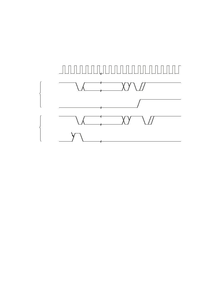
ADSP-BF535
34
REV. A
Universal Asynchronous Receiver-Transmitter (UART)
Port--Receive and Transmit Timing
Figure 17
describes UART port receive and transmit operations.
The maximum baud rate is SCLK/16. As shown in
Figure 17
,
there is some latency between the generation of internal UART
interrupts and the external data operations. These latencies are
negligible at the data transmission rates for the UART.
Figure 17. UART Port--Receive and Transmit Timing
RxD
DATA(58)
INTERNAL
UART RECEIVE
INTERRUPT
UART RECEIVE BIT SET BY DATA
STOP; CLEARED BY FIFO READ
SCLK
(SAMPLE
CLOCK)
TxD
DATA(58)
STOP (12)
INTERNAL
UART TRANSMIT
INTERRUPT
UART TRANSMIT BIT SET BY PROGRAM;
CLEARED BY WRITE TO TRANSMIT
START
STOP
TRANSMIT
RECEIVE
AS DATA
WRITTEN TO
BUFFER
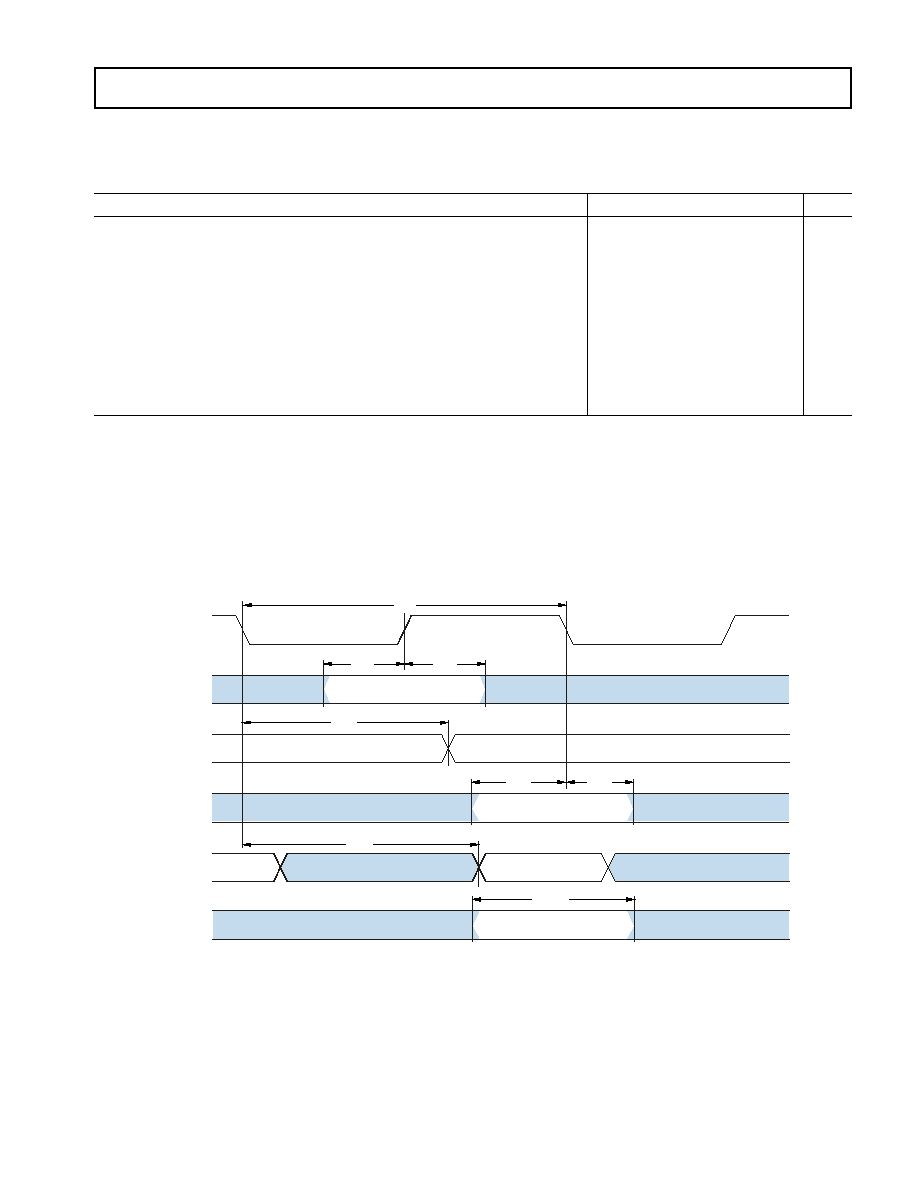
35
REV. A
ADSP-BF535
JTAG Test and Emulation Port Timing
Table 25
and
Figure 18
describe JTAG port operations.
Table 25. JTAG Port Timing
Parameter
Min
Max
Unit
Timing Requirements
t
TCK
TCK Period
20.0
ns
t
STAP
TDI, TMS Setup Before TCK High
4.0
ns
t
HTAP
TDI, TMS Hold After TCK High
4.0
ns
t
SSYS
System Inputs Setup Before TCK Low
1
4.0
ns
t
HSYS
System Inputs Hold After TCK Low
1
5.0
ns
t
TRSTW
TRST Pulse Width
2
4.0
ns
Switching Characteristics
t
DTDO
TDO Delay from TCK Low
7.0
ns
t
DSYS
System Outputs Delay After TCK Low
3
0.0
15.0
ns
1
System Inputs =DATA31-0, ADDR25-2, ARDY, TMR2-0, PF15-0, RSCLK0, RFS0, DR0, TSCLK0, TFS0, RSCLK1, RFS1, DR1, TSCLK1, TFS1,
MOSI0, MISO0, SCK0, MOSI1, MISO1, SCK1, RX0, RX1, USB_CLK, XVER_DATA, DPLS, DMNS, NMI,
RESET, BYPASS, BMODE2-0,
PCI_AD31-0,
PCI_CBE3-0, PCI_FRAME, PCI_IRDY, PCI_TRDY, PCI_DEVSEL, PCI_STOP, PCI_PERR, PCI_PAR, PCI_SERR, PCI_RST,
PCI_GNT, PCI_IDSEL, PCI_LOCK, PCI_CLK, PCI_INTA, PCI_INTB, PCI_INTC, PCI_INTD.
2
50 MHz max.
3
System Outputs=DATA31-0, ADDR25-2,
ABE3-0/SDQM3-0, AOE, ARE, AWE, SCAS, CLKOUT/SCLK1, SCLK0, SCKE, SA10, SWE, SMS3-0,
SRAS, TMR2-0, PF15-0, RSCLK0, RFS0, TSCLK0, TFS0, DT0, RSCLK1, RFS1, TSCLK1, TFS1, DT1, MOSI0, MISO0, SCK0, MOSI1, MISO1,
SCK1, TX0, TX1, TXDPLS, TXDMNS,
TXEN, SUSPEND, DEEPSLEEP, PCI_AD31-0, PCI_CBE3-0, PCI_FRAME, PCI_IRDY, PCI_TRDY,
PCI_DEVSEL, PCI_STOP, PCI_PERR, PCI_PAR, PCI_REQ, PCI_SERR, PCI_RST, PCI_INTA, EMU.
Figure 18. JTAG Port Timing
T M S
T D I
T D O
S Y S T E M
IN P U T S
S Y S T E M
O U T P U T S
T C K
t
T C K
t
H T A P
t
S T A P
t
D T D O
t
S S Y S
t
H S Y S
t
D S Y S
t
T R S T W
T R ST
ADSP-BF535
36
REV. A
Output Drive Currents
Figure 19
through
Figure 21
show typical current-voltage char-
acteristics for the output drivers of the ADSP-BF535 Blackfin
processor. The curves represent the current drive capability of
the output drivers as a function of output voltage.
Figure 19
applies to the
ABE30, SDQM30, ADDR252, AMS30,
AOE, ARE, AWE, CLKOUT, SCLK1, DATA310, DT10,
EMU, MISO10, MOSI10, PF150, RFS10, RSCLK10,
SA10,
SCAS, SCK10, SCKE, SCLK0, DEEPSLEEP,
SMS30, SRAS, SUSPEND, SWE, TDO, TFS10, TMR20,
TSCLK10, TX10, TXDMNS, TXDPLS,
TXEN, and
XTAL0 pins.
Figure 20
applies to the PCI_AD310,
PCI_CBE30, PCI_DEVSEL, PCI_FRAME, PCI_INTA,
PCI_IRDY, PCI_PAR, PCI_PERR, PCI_RST, PCI_SERR,
PCI_STOP, and PCI_TRDY pins.
Figure 21
applies to the
PCI_REQ pin.
Power Dissipation
Total power dissipation has two components: one due to internal
circuitry (P
INT
) and one due to the switching of external output
drivers (P
EXT
).
Table 26
shows the power dissipation for internal
circuitry (V
DDINT
). Internal power dissipation is dependent on the
instruction execution sequence and the data operands involved.
Table 27
shows the power dissipation for the phase-locked loop
(PLL) circuitry (V
DDPLL
).
The external component of total power dissipation is caused by
the switching of output pins. Its magnitude depends on:
·
Maximum frequency (f
0
) at which all output pins can
switch during each cycle
·
Their load capacitance (C
0
) of all switching pins
·
Their voltage swing (V
DDEXT
)
The external component is calculated using:
Figure 19. Output Drive Current
Figure 20. PCI 33 MHz Output Drive Current
200
150
100
50
0
100
150
200
50
V
OH
(V
DDEXT
= 3.45V,
40°C)
V
OH
(V
DDEXT
= 3.45V, 0°C)
V
OH
(V
DDEXT
= 3.15V, +105°C)
V
OH
(V
DDEXT
= 2.5V, +85°C)
V
OH
(V
DDEXT
= 3.3V, +25°C)
V
OL
(V
DDEXT
= 3.3V, +25°C)
V
OL
(V
DDEXT
= 2.5V, +85°C)
V
OL
(V
DDEXT
= 3.45V, 0°C)
V
OL
(V
DDEXT
= 3.15V, +105°C)
V
OL
(V
DDEXT
= 3.45V,
40°C)
SOURCE (V
O
) VOLTAGE V
0
3.5
0.5
1.0
1.5
2.0
2.5
3.0
4.0
S
O
U
R
C
E
(
I
O
)
C
U
R
R
E
N
T
m
A
0
3.5
0.5
1.0
1.5
2.0
2.5
3.0
4.0
200
150
100
50
0
50
100
150
V
OH
(V
DDEXT
= 3.3V, +25°C)
V
OH
(V
DDEXT
= 2.5V,
+85°C)
V
OH
(V
DDEXT
= 3.45V, 0°C)
V
OH
(V
DDEXT
= 3.15V, +105°C)
V
OH
(V
DDEXT
= 3.45V,
45°C)
V
OL
(V
DDEXT
= 3.3V, +25°C)
V
OL
(V
DDEXT
= 2.5V, +85°C)
V
OL
(V
DDEXT
= 3.45V, 0°C)
V
OL
(V
DDEXT
= 3.15V, +105°C)
V
OL
(V
DDEXT
= 3.45V,
45°C)
S
O
U
R
C
E
(
I
O
)
C
U
R
R
E
N
T
m
A
SOURCE (V
O
) VOLTAGE V
200
250
300
Figure 21. PCI_REQ Output Drive Current
Table 26. Internal Power Dissipation
Test Conditions
1
1
I
DD
data is specified for typical process parameters. All data at 25ºC.
Parameter
f
CCLK
=
100 MHz
V
DDINT
=
1.0 V
f
CCLK
=
200 MHz
V
DDINT
=
1.2 V
f
CCLK
=
300 MHz
V
DDINT
=
1.5 V
f
CCLK
=
350 MHz
V
DDINT
=
1.6 V
Unit
I
DDTYP
2
2
Processor executing 75% dual Mac, 25% ADD with moderate data bus
activity.
96.0
206.0
387.0
498.0
mA
I
DDEFR
3
3
Implementation of Enhanced Full Rate (EFR) GSM algorithm.
114.0
248.0
463.0
579.0
mA
I
DDSLEEP
4
4
See the ADSP-BF535 Blackfin Processor Hardware Reference Manual for
definitions of Sleep and Deep Sleep operating modes.
15.0
29.0
52.0
62.0
mA
I
DDDEEPSLEEP
4
4.0
5.0
8.2
9.8
mA
I
DDRESET
5
5
I
DD
is specified for when the device is in the reset state.
132.0
255.0
485.3
651.0
mA
SOURCE (V
O
) VOLTAGE V
S
O
U
R
C
E
(
I
O
)
C
U
R
R
E
N
T
m
A
0
3.5
0.5
1.0
1.5
2.0
2.5
3.0
4.0
200
150
100
50
0
50
100
150
200
V
OH
(V
DDEXT
= 3.3V, +25°C)
V
OH
(V
DDEXT
= 2.5V, +85°C)
V
OH
(V
DDEXT
= 3.45V, 0°C)
V
OH
(V
DDEXT
= 3.15V,
+105°C)
V
OH
(V
DDEXT
= 3.45V,
45°C)
V
OL
(V
DDEXT
= 3.3V, +25°C)
V
OL
(V
DDEXT
= 2.5V, +85°C)
V
OL
(V
DDEXT
= 3.45V, 0°C)
V
OL
(V
DDEXT
= 3.15V, +105°C)
V
OL
(V
DDEXT
= 3.45V,
45°C)
P
EXT
V
DDEXT
2
C
0
f
0
×
×
=
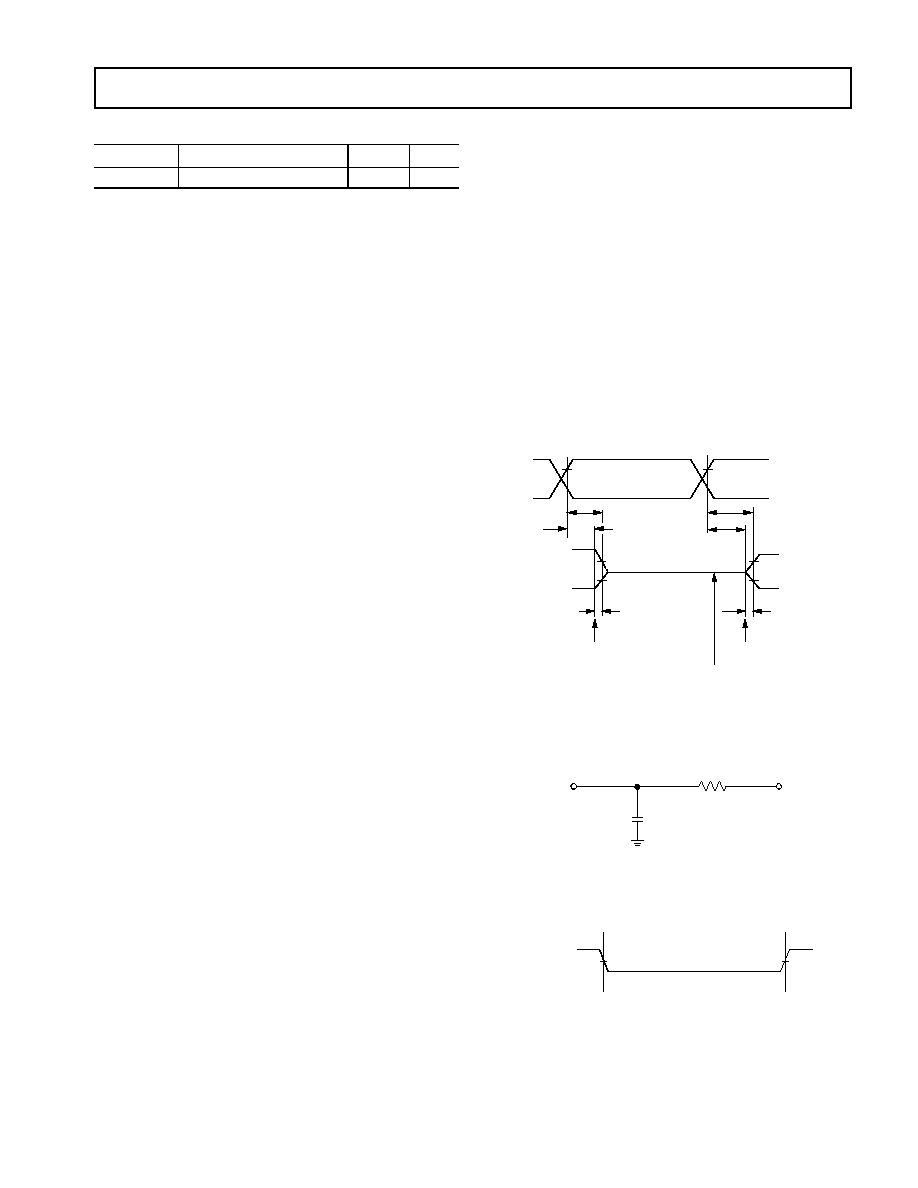
37
REV. A
ADSP-BF535
The frequency f includes driving the load high and then back low.
For example: DATA310 pins can drive high and low at a
maximum rate of 1/(2
t
SCLK
) while in SDRAM burst mode.
A typical power consumption can now be calculated for these
conditions by adding a typical internal power dissipation:
Note that the conditions causing a worst-case P
EXT
differ from
those causing a worst-case P
INT
. Maximum P
INT
cannot occur
while 100% of the output pins are switching from all ones (1s) to
all zeros (0s). Note, as well, that it is not common for an appli-
cation to have 100% or even 50% of the outputs switching
simultaneously.
Test Conditions
All timing parameters appearing in this data sheet were measured
under the conditions described in this section.
Output Enable Time
Output pins are considered to be enabled when they have made
a transition from a high impedance state to the point when they
start driving. The output enable time t
ENA
is the interval from the
point when a reference signal reaches a high or low voltage level
to the point when the output starts driving as shown in the Output
Enable/Disable diagram (
Figure 22
). The time t
ENA_MEASURED
is
the interval from when the reference signal switches to when the
output voltage reaches 2.0 V (output high) or 1.0 V (output low).
Time t
TRIP
is the interval from when the output starts driving to
when the output reaches the 1.0 V or 2.0 V trip voltage. Time
t
ENA
is calculated as shown in the equation:
If multiple pins (such as the data bus) are enabled, the measure-
ment value is that of the first pin to start driving.
Output Disable Time
Output pins are considered to be disabled when they stop driving,
go into a high impedance state, and start to decay from their
output high or low voltage. The time for the voltage on the bus
to decay by
V is dependent on the capacitive load, C
L
and the
load current, I
L
. This decay time can be approximated by the
equation:
The output disable time t
DIS
is the difference between
t
DIS_MEASURED
and t
DECAY
as shown in
Figure 22
. The time
t
DIS_MEASURED
is the interval from when the reference signal
switches to when the output voltage decays
V from the measured
output high or output low voltage. The time t
DECAY
is calculated
with test loads C
L
and I
L
, and with
V equal to 0.5 V.
Example System Hold Time Calculation
To determine the data output hold time in a particular system,
first calculate t
DECAY
using the equation given above. Choose
V
to be the difference between the ADSP-BF535 Blackfin proces-
sor's output voltage and the input threshold for the device
requiring the hold time. A typical
V will be 0.4 V. C
L
is the total
bus capacitance (per data line), and I
L
is the total leakage or three-
state current (per data line). The hold time will be t
DECAY
plus the
minimum disable time (for example, t
DSDAT
for an SDRAM write
cycle).
Table 27. PLL Power Dissipation
Parameter
Test Conditions
Typical
Unit
I
DDPLL
V
DDPLL
= 1.5 V, 25ºC
4.0
mA
P
TOTAL
P
EXT
I
(
DD
V
DDINT
×
)
+
=
t
ENA
t
ENA_MEASURED
=
t
TRIP
t
DECAY
C
L
V
(
)
I
L
/
=
Figure 22. Output Enable/Disable
Figure 23. Equivalent Device Loading for AC
Measurements (Includes All Fixtures)
Figure 24. Voltage Reference Levels for AC
Measurements (Except Output Enable/Disable)
REFERENCE
SIGNAL
t
DIS
OUTPUT STARTS DRIVING
V
OH
(MEASURED)
V
V
OL
(MEASURED) +
V
t
DIS_MEASURED
V
OH
(MEASURED)
V
OL
(MEASURED)
2.0V
1.0V
V
OH
(MEASURED)
V
OL
(MEASURED)
HIGH IMPEDANCE STATE.
TEST CONDITIONS CAUSE THIS
VOLTAGE TO BE APPROXIMATELY 1.5V.
OUTPUT STOPS DRIVING
t
ENA
t
DECAY
t
ENA-MEASURED
t
TRIP
1.5V
30pF
TO
OUTPUT
PIN
50
INPUT
OR
OUTPUT
1.5V
1.5V

ADSP-BF535
38
REV. A
Environmental Conditions
The ADSP-BF535 is offered in a 260-ball PBGA package.
To determine the junction temperature on the application printed
circuit board use:
where:
T
J
= Junction temperature ( C)
T
CASE
= Case temperature ( C) measured by customer at top
center of package.
JT
= From
Table 28
P
D
= Power dissipation (see
Power Dissipation on Page 36
for the
method to calculate P
D
)
Values of
JA
are provided for package comparison and printed
circuit board design considerations.
JA
can be used for a first
order approximation of T
J
by the equation:
where:
T
A
= Ambient temperature ( C)
Values of
JC
are provided for package comparison and printed
circuit board design considerations when an external heatsink is
required.
Values of
JB
are provided for package comparison and printed
circuit board design considerations.
In
Table 28
, airflow measurements comply with JEDEC
standards JESD51-2 and JESD51-6, and the junction-to-board
measurement complies with JESD51-8. The junction-to-case
measurement complies with MIL-STD-883 (Method 1012.1).
All measurements use a 2S2P JEDEC test board.
T
J
T
CASE
JT
P
D
×
(
)
+
=
T
J
T
A
JA
P
D
×
(
)
+
=
Table 28. Thermal Characteristics
Parameter
Condition
Typical
Unit
JA
0 linear m/s air flow
23.8
C/W
JMA
1 linear m/s air flow
20.8
C/W
JMA
2 linear m/s air flow
19.8
C/W
JB
9.95
C/W
JC
9.35
C/W
JT
0 linear m/s air flow
0.30
C/W

39
REV. A
ADSP-BF535
260-Ball PBGA Pinout
Table 29
lists the PBGA pinout by signal name.
Table 30 on
Page 41
lists the pinout by pin number.
Table 29. 260-Ball PBGA Pin Assignment (Alphabetically by Signal)
Signal
Pin
Signal
Pin
Signal
Pin
Signal
Pin
ABE0/SDQM0
E02
DATA5
R02
GND
K08
PCI_AD25
M16
ABE1/SDQM1
B01
DATA6
P03
GND
K09
PCI_AD26
N17
ABE2/SDQM2
G03
DATA7
U01
GND
K10
PCI_AD27
P17
ABE3/SDQM3
H07
DATA8
U02
GND
K11
PCI_AD28
P15
ADDR2
A06
DATA9
T02
GND
K12
PCI_AD29
N16
ADDR3
B06
DATA10
V02
GND
L07
PCI_AD30
R17
ADDR4
D06
DATA11
V03
GND
L08
PCI_AD31
P16
ADDR5
C06
DATA12
R04
GND
L09
PCI_CBE0
F16
ADDR6
A05
DATA13
U03
GND
L10
PCI_CBE1
F15
ADDR7
B05
DATA14
T03
GND
L11
PCI_CBE2
E16
ADDR8
A04
DATA15
T04
GND
M07
PCI_CBE3
D17
ADDR9
C05
DATA16
U04
GND
M09
PCI_CLK
D14
ADDR10
D05
DATA17
V04
GND
M10
PCI_DEVSEL
C16
ADDR11
B04
DATA18
V05
MISO0
T16
PCI_FRAME
C17
ADDR12
A01
DATA19
R05
MISO1
U18
PCI_GNT
C18
ADDR13
C04
DATA20
T05
MOSI0
U16
PCI_IDSEL
B18
ADDR14
D04
DATA21
U05
MOSI1
T17
PCI_INTA
C14
ADDR15
A03
DATA22
V06
N/C
A18
PCI_INTB
B15
ADDR16
B03
DATA23
R06
N/C
R03
PCI_INTC
A15
ADDR17
A02
DATA24
U06
N/C
V01
PCI_INTD
D13
ADDR18
C03
DATA25
T06
N/C
V18
PCI_IRDY
E15
ADDR19
D03
DATA26
V07
NMI
B11
PCI_LOCK
A16
ADDR20
B02
DATA27
V08
PCI_AD0
E17
PCI_PAR
C15
ADDR21
C02
DATA28
U07
PCI_AD1
E18
PCI_PERR
D15
ADDR22
E03
DATA29
R07
PCI_AD2
G16
PCI_REQ
D16
ADDR23
C01
DATA30
T07
PCI_AD3
F17
PCI_RST
D18
ADDR24
F03
DATA31
V09
PCI_AD4
F18
PCI_SERR
B16
ADDR25
D02
DMNS
D08
PCI_AD5
G18
PCI_STOP
A17
AMS0
F02
DPLS
C09
PCI_AD6
G17
PCI_TRDY
B17
AMS1
D01
DR0
V14
PCI_AD7
H18
PF0/
SPISS0/MSEL0
U08
AMS2
H03
DR1
U15
PCI_AD8
J18
PF1/
SPISS1/MSEL1
R08
AMS3
G02
DT0
R14
PCI_AD9
H17
PF2/
SPI0SEL1/MSEL2
T08
AOE
E01
DT1
V17
PCI_AD10
K18
PF3/
SPI1SEL1/MSEL3
V10
ARDY
R01
EMU
A13
PCI_AD11
H16
PF4/
SPI0SEL2/MSEL4
U09
ARE
F01
GND
C13
PCI_AD12
L18
PF5/
SPI1SEL2/MSEL5
R09
AWE
G01
GND
H02
PCI_AD13
J17
PF6/
SPI0SEL3/MSEL6
T09
BMODE0
B14
GND
H08
PCI_AD14
M18
PF7/
SPI1SEL3/DF
R11
BMODE1
A14
GND
H10
PCI_AD15
K17
PF8/
SPI0SEL4/SSEL0
T11
BMODE2
B13
GND
H11
PCI_AD16
J16
PF9/
SPI1SEL4/SSEL1
U11
BYPASS
C12
GND
J07
PCI_AD17
K16
PF10/
SPI0SEL5
V12
CLKIN1
D09
GND
J08
PCI_AD18
N18
PF11/
SPI1SEL5
T12
CLKOUT/SCLK1
H01
GND
J09
PCI_AD19
P18
PF12/
SPI0SEL6
R12
DATA0
N02
GND
J10
PCI_AD20
L17
PF13/
SPI1SEL6
U12
DATA1
M03
GND
J11
PCI_AD21
L16
PF14/
SPI0SEL7
V13
DATA2
T01
GND
J12
PCI_AD22
R18
PF15/
SPI1SEL7
T13
DATA3
P02
GND
K02
PCI_AD23
T18
RESET
B09
DATA4
N03
GND
K07
PCI_AD24
M17
RFS0
U13

ADSP-BF535
40
REV. A
RFS1
V16
SWE
J03
USB_CLK
G07
V
DDINT
L12
RSCLK0
R13
TCK
D10
V
DDEXT
E04
V
DDINT
M08
RSCLK1
U14
TDI
C11
V
DDEXT
G04
V
DDINT
M11
RX0
A07
TDO
D11
V
DDEXT
G08
V
DDINT
M12
RX1
B08
TFS0
T14
V
DDEXT
J01
V
DDINT
N04
SA10
M01
TFS1
R15
V
DDEXT
J02
V
DDINT
N15
SCAS
L03
TMR0
B07
V
DDEXT
J04
V
DDPCIEXT
H15
SCK0
U17
TMR1
C07
V
DDEXT
K04
V
DDPCIEXT
J15
SCK1
R16
TMR2
D07
V
DDEXT
L04
V
DDPCIEXT
K15
SCKE
L01
TMS
A12
V
DDEXT
M04
V
DDPCIEXT
L15
SCLK0
K01
TRST
B12
V
DDEXT
P04
V
DDPCIEXT
M15
DEEPSLEEP
D12
TSCLK0
V15
V
DDINT
F04
V
DDPLL
G09
SMS0
M02
TSCLK1
T15
V
DDINT
G11
V
DDRTC
U10
SMS1
P01
TX0
A08
V
DDINT
G12
V
SSPLL
A10
SMS2
N01
TX1
C08
V
DDINT
G15
V
SSRTC
V11
SMS3
K03
TXDMNS
G10
V
DDINT
H04
XTAL1
R10
SRAS
L02
TXDPLS
B10
V
DDINT
H09
XTAL0
T10
SUSPEND
A11
TXEN
C10
V
DDINT
H12
XVER_DATA
A09
Table 29. 260-Ball PBGA Pin Assignment (Alphabetically by Signal) (continued)
Signal
Pin
Signal
Pin
Signal
Pin
Signal
Pin

41
REV. A
ADSP-BF535
Table 30. 260-Ball PBGA Pin Assignment (Numerically by Pin Number)
Pin
Signal
Pin
Signal
Pin
Signal
Pin
Signal
A01
ADDR12
D12
DEEPSLEEP
K01
SCLK0
R08
PF1/
SPISS1/MSEL1
A02
ADDR17
D13
PCI_INTD
K02
GND
R09
PF5/
SPI1SEL2/MSEL5
A03
ADDR15
D14
PCI_CLK
K03
SMS3
R10
XTAL1
A04
ADDR8
D15
PCI_PERR
K04
V
DDEXT
R11
PF7/
SPI1SEL3/DF
A05
ADDR6
D16
PCI_REQ
K07
GND
R12
PF12/
SPI0SEL6
A06
ADDR2
D17
PCI_CBE3
K08
GND
R13
RSCLK0
A07
RX0
D18
PCI_RST
K09
GND
R14
DT0
A08
TX0
E01
AOE
K10
GND
R15
TFS1
A09
XVER_DATA
E02
ABE0/SDQM0
K11
GND
R16
SCK1
A10
V
SSPLL
E03
ADDR22
K12
GND
R17
PCI_AD30
A11
SUSPEND
E04
V
DDEXT
K15
V
DDPCIEXT
R18
PCI_AD22
A12
TMS
E15
PCI_IRDY
K16
PCI_AD17
T01
DATA2
A13
EMU
E16
PCI_CBE2
K17
PCI_AD15
T02
DATA9
A14
BMODE1
E17
PCI_AD0
K18
PCI_AD10
T03
DATA14
A15
PCI_INTC
E18
PCI_AD1
L01
SCKE
T04
DATA15
A16
PCI_LOCK
F01
ARE
L02
SRAS
T05
DATA20
A17
PCI_STOP
F02
AMS0
L03
SCAS
T06
DATA25
A18
N/C
F03
ADDR24
L04
V
DDEXT
T07
DATA30
B01
ABE1/SDQM1
F04
V
DDINT
L07
GND
T08
PF2/
SPI0SEL1/MSEL2
B02 ADDR20
F15
PCI_CBE1
L08
GND
T09
PF6/
SPI0SEL3/MSEL6
B03 ADDR16
F16
PCI_CBE0
L09
GND
T10
XTAL0
B04 ADDR11
F17
PCI_AD3
L10
GND
T11
PF8/
SPI0SEL4/SSEL0
B05 ADDR7
F18
PCI_AD4
L11
GND
T12
PF11/
SPI1SEL5
B06 ADDR3
G01
AWE
L12
V
DDINT
T13
PF15/
SPI1SEL7
B07
TMR0
G02
AMS3
L15
V
DDPCIEXT
T14
TFS0
B08
RX1
G03
ABE2/SDQM2
L16
PCI_AD21
T15
TSCLK1
B09
RESET
G04
V
DDEXT
L17
PCI_AD20
T16
MISO0
B10
TXDPLS
G07
USB_CLK
L18
PCI_AD12
T17
MOSI1
B11
NMI
G08
V
DDEXT
M01
SA10
T18
PCI_AD23
B12
TRST
G09
V
DDPLL
M02
SMS0
U01
DATA7
B13
BMODE2
G10
TXDMNS
M03
DATA1
U02
DATA8
B14
BMODE0
G11
V
DDINT
M04
V
DDEXT
U03
DATA13
B15
PCI_INTB
G12
V
DDINT
M07
GND
U04
DATA16
B16
PCI_SERR
G15
V
DDINT
M08
V
DDINT
U05
DATA21
B17
PCI_TRDY
G16
PCI_AD2
M09
GND
U06
DATA24
B18
PCI_IDSEL
G17
PCI_AD6
M10
GND
U07
DATA28
C01
ADDR23
G18
PCI_AD5
M11
V
DDINT
U08
PF0/
SPISS0/MSEL0
C02
ADDR21
H01
CLKOUT/SCLK1
M12
V
DDINT
U09
PF4/
SPI0SEL2/MSEL4
C03
ADDR18
H02
GND
M15
V
DDPCIEXT
U10
V
DDRTC
C04
ADDR13
H03
AMS2
M16
PCI_AD25
U11
PF9/
SPI1SEL4/SSEL1
C05
ADDR9
H04
V
DDINT
M17
PCI_AD24
U12
PF13/
SPI1SEL6
C06
ADDR5
H07
ABE3/SDQM3
M18
PCI_AD14
U13
RFS0
C07
TMR1
H08
GND
N01
SMS2
U14
RSCLK1
C08
TX1
H09
V
DDINT
N02
DATA0
U15
DR1
C09
DPLS
H10
GND
N03
DATA4
U16
MOSI0
C10
TXEN
H11
GND
N04
V
DDINT
U17
SCK0
C11
TDI
H12
V
DDINT
N15
V
DDINT
U18
MISO1
C12
BYPASS
H15
V
DDPCIEXT
N16
PCI_AD29
V01
N/C
C13
GND
H16
PCI_AD11
N17
PCI_AD26
V02
DATA10

ADSP-BF535
42
REV. A
C14
PCI_INTA
H17
PCI_AD9
N18
PCI_AD18
V03
DATA11
C15
PCI_PAR
H18
PCI_AD7
P01
SMS1
V04
DATA17
C16
PCI_DEVSEL
J01
V
DDEXT
P02
DATA3
V05
DATA18
C17
PCI_FRAME
J02
V
DDEXT
P03
DATA6
V06
DATA22
C18
PCI_GNT
J03
SWE
P04
V
DDEXT
V07
DATA26
D01
AMS1
J04
V
DDEXT
P15
PCI_AD28
V08
DATA27
D02
ADDR25
J07
GND
P16
PCI_AD31
V09
DATA31
D03
ADDR19
J08
GND
P17
PCI_AD27
V10
PF3/
SPI1SEL1/MSEL3
D04
ADDR14
J09
GND
P18
PCI_AD19
V11
V
SSRTC
D05
ADDR10
J10
GND
R01
ARDY
V12
PF10/
SPI0SEL5
D06
ADDR4
J11
GND
R02
DATA5
V13
PF14/
SPI0SEL7
D07
TMR2
J12
GND
R03
N/C
V14
DR0
D08
DMNS
J15
V
DDPCIEXT
R04
DATA12
V15
TSCLK0
D09
CLKIN1
J16
PCI_AD16
R05
DATA19
V16
RFS1
D10
TCK
J17
PCI_AD13
R06
DATA23
V17
DT1
D11
TDO
J18
PCI_AD8
R07
DATA29
V18
N/C
Table 30. 260-Ball PBGA Pin Assignment (Numerically by Pin Number) (continued)
Pin
Signal
Pin
Signal
Pin
Signal
Pin
Signal
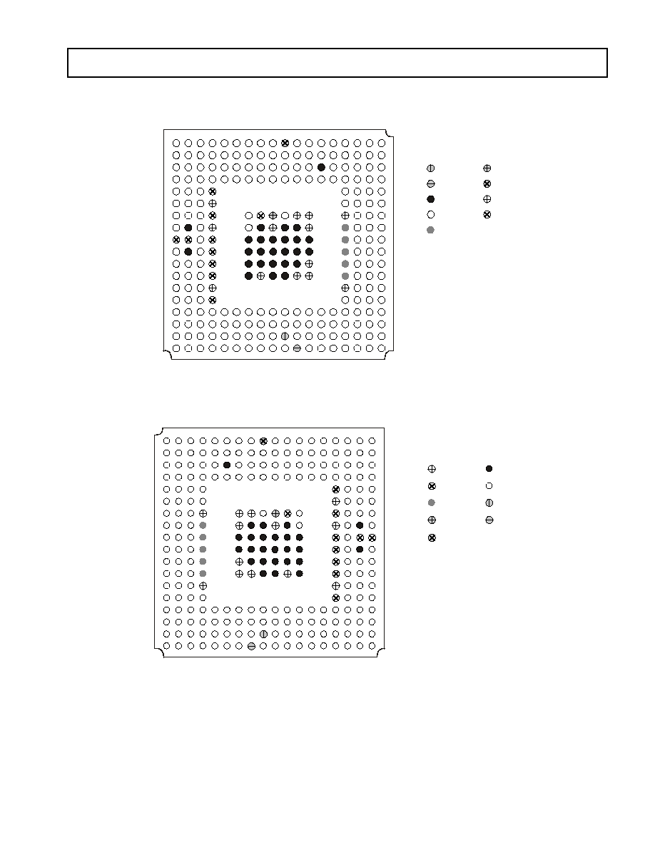
43
REV. A
ADSP-BF535
Figure 25. 260-Ball Metric PBGA Pin Configuration (Top View)
Figure 26. 260-Ball Metric PBGA Pin Configuration (Bottom View)
A
B
C
D
E
F
G
H
J
K
L
M
N
P
R
T
U
V
1
2
3
4
5
6
7
8
9
10 11 12 13 14 15 16 17 18
V
DDINT
V
DDEXT
GND
V
DDPCIEXT
I/O
KEY:
V
DDPLL
V
SSPLL
V
SSRTC
V
DDRTC
A
B
C
D
E
F
G
H
J
K
L
M
N
P
R
T
U
V
1
2
3
4
5
6
7
8
9
10
11
12
13
14
15
16
17
18
V
DDINT
V
DDEXT
GND
V
DDPCIEXT
I/O
KEY:
V
DDPLL
V
SSPLL
V
SSRTC
V
DDRTC
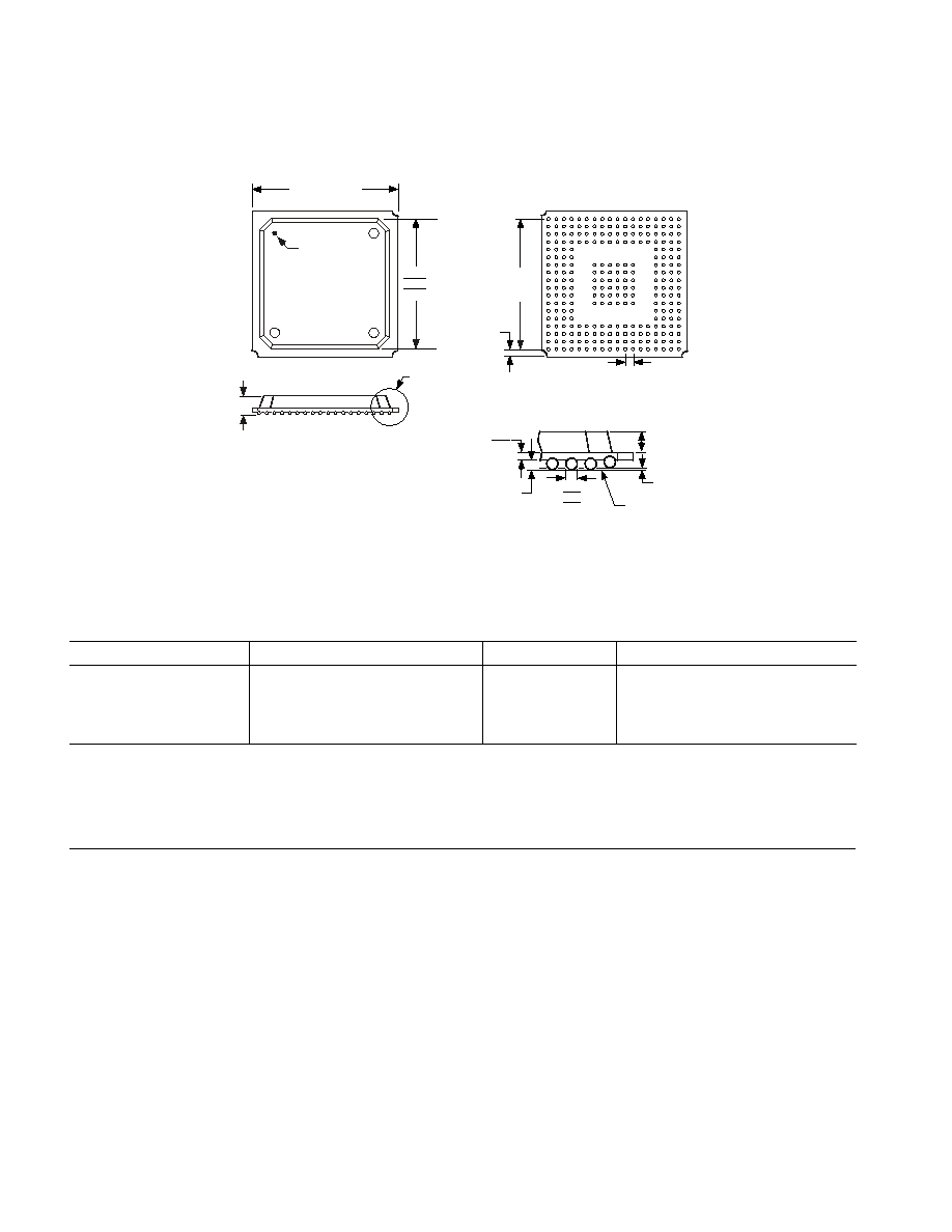
ADSP-BF535
44
REV. A
C
0
4
4
1
3
0
9
/0
4(
A)
OUTLINE DIMENSIONS
ORDERING GUIDE
Revision History
Figure 27. 260-Ball Metric Plastic Ball Grid Array (PBGA) (B-260)
Part Number
Temperature Range (Ambient)
Instruction Rate
Operating Voltage (V)
ADSP-BF535PKB-350 0ºC
to
+70ºC
350 MHz
1.0 V to 1.6 V internal, 3.3 V I/O
ADSP-BF535PKB-300 0ºC
to
+70ºC
300 MHz
1.0 V to 1.5 V internal, 3.3 V I/O
ADSP-BF535PBB-300
40ºC to +85ºC
300 MHz
1.0 V to 1.5 V internal, 3.3 V I/O
ADSP-BF535PBB-200
40ºC to +85ºC
200 MHz
1.0 V to 1.5 V internal, 3.3 V I/O
Location
Page
9/04--Data Sheet Changed from REV. 0 to REV. A
Changes to Clock Signals Section ........................................................................................................................ 13
Changes to Recommended Operating Conditions Footnote References ................................................................. 21
Changes to Electrical Characteristics ................................................................................................................... 21
Change to Table 11 ............................................................................................................................................ 24
Change to Figure 11 ............................................................................................................................................ 27
Change to Figure 12 ........................................................................................................................................... 28
Change to Output Drive Currents Section ............................................................................................................ 36
Replaced Figures 19, 20, and 21 .......................................................................................................................... 36
Changes to Power Dissipation Section ................................................................................................................. 36
Change to Table 26 ............................................................................................................................................ 36
DETAIL A
2.50
MAX
SEATING
PLANE
0.65
0.45
0.40
MIN
0.70
0.60
0.50
BALL DIAMETER
0.20
MAX, TYP
1.22
MAX
DETAIL A
TOP VIEW
BALL A1
INDICATOR
19.00 BSC SQ
17.05
16.95 SQ
16.85
15 13 11 9
7
5
3
1
17
16 14 12 10 8
6
4
2
18
BOTTOM VIEW
1.00 BSC
BALL PITCH
17.00
BSC
SQ
1.00
BSC
NOTES
1.
ALL DIMENSIONS ARE IN MILLIMETERS.
2. THE ACTUAL POSITION OF THE BALL GRID
IS WITHIN 0.25 MM OF ITS IDEAL POSITION
RELATIVE TO THE PACKAGE EDGES.
3. THE ACTUAL POSITION OF EACH BALL IS
WITHIN 0.10 MM OF ITS IDEAL POSITION RELATIVE
TO THE BALL GRID.
4. CENTER DIMENSIONS ARE NOMINAL.
5. COMPLIANT TO JEDEC REGISTERED OUTLINE
MS-034, VARIATION AAG-1.
A
B
C
D
E
F
G
H
J
K
L
M
N
P
R
T
U
V
Document Outline