ADSP-BF534/ADSP-BF536/ADSP-BF537 Blackfin® Embedded Processor Data Sheet (Rev. B)
a
Blackfin and the Blackfin logo are registered trademarks of Analog Devices, Inc.
Blackfin
®
Embedded Processor
ADSP-BF534/ADSP-BF536/ADSP-BF537
Rev. B
Information furnished by Analog Devices is believed to be accurate and reliable.
However, no responsibility is assumed by Analog Devices for its use, nor for any
infringements of patents or other rights of third parties that may result from its use.
Specifications subject to change without notice. No license is granted by implication
or otherwise under any patent or patent rights of Analog Devices. Trademarks and
registered trademarks are the property of their respective owners.
One Technology Way, P.O. Box 9106, Norwood, MA 02062-9106 U.S.A.
Tel: 781.329.4700
www.analog.com
Fax: 781.461.3113
©2006 Analog Devices, Inc. All rights reserved.
FEATURES
Up to 600 MHz high performance Blackfin processor
Two 16-bit MACs, two 40-bit ALUs, four 8-bit video ALUs,
40-bit shifter
RISC-like register and instruction model for ease of
programming and compiler-friendly support
Advanced debug, trace, and performance monitoring
0.8 V to 1.2 V core V
DD
with on-chip voltage regulation
2.5 V and 3.3 V-tolerant I/O with specific 5 V-tolerant pins
182-ball and 208-ball MBGA packages
MEMORY
Up to 132K bytes of on-chip memory comprised of:
Instruction SRAM/cache; instruction SRAM;
data SRAM/cache; additional dedicated data SRAM;
scratchpad SRAM (see
Table 1 on Page 3
for available
memory configurations)
External memory controller with glueless support for SDRAM
and asynchronous 8-bit and 16-bit memories
Flexible booting options from external flash, SPI and TWI
memory or from SPI, TWI, and UART host devices
Memory management unit providing memory protection
PERIPHERALS
IEEE 802.3-compliant 10/100 Ethernet MAC (ADSP-BF536 and
ADSP-BF537 only)
Controller area network (CAN) 2.0B interface
Parallel peripheral interface (PPI), supporting ITU-R 656
video data formats
Two dual-channel, full-duplex synchronous serial ports
(SPORTs), supporting eight stereo I
2
S channels
12 peripheral DMAs, 2 mastered by the Ethernet MAC
Two memory-to-memory DMAs with external request lines
Event handler with 32 interrupt inputs
Serial peripheral interface (SPI)-compatible
Two UARTs with IrDA
®
support
Two-wire interface (TWI) controller
Eight 32-bit timer/counters with PWM support
Real-time clock (RTC) and watchdog timer
32-bit core timer
48 general-purpose I/Os (GPIOs), 8 with high current drivers
On-chip PLL capable of 1 to 63 frequency multiplication
Debug/JTAG interface
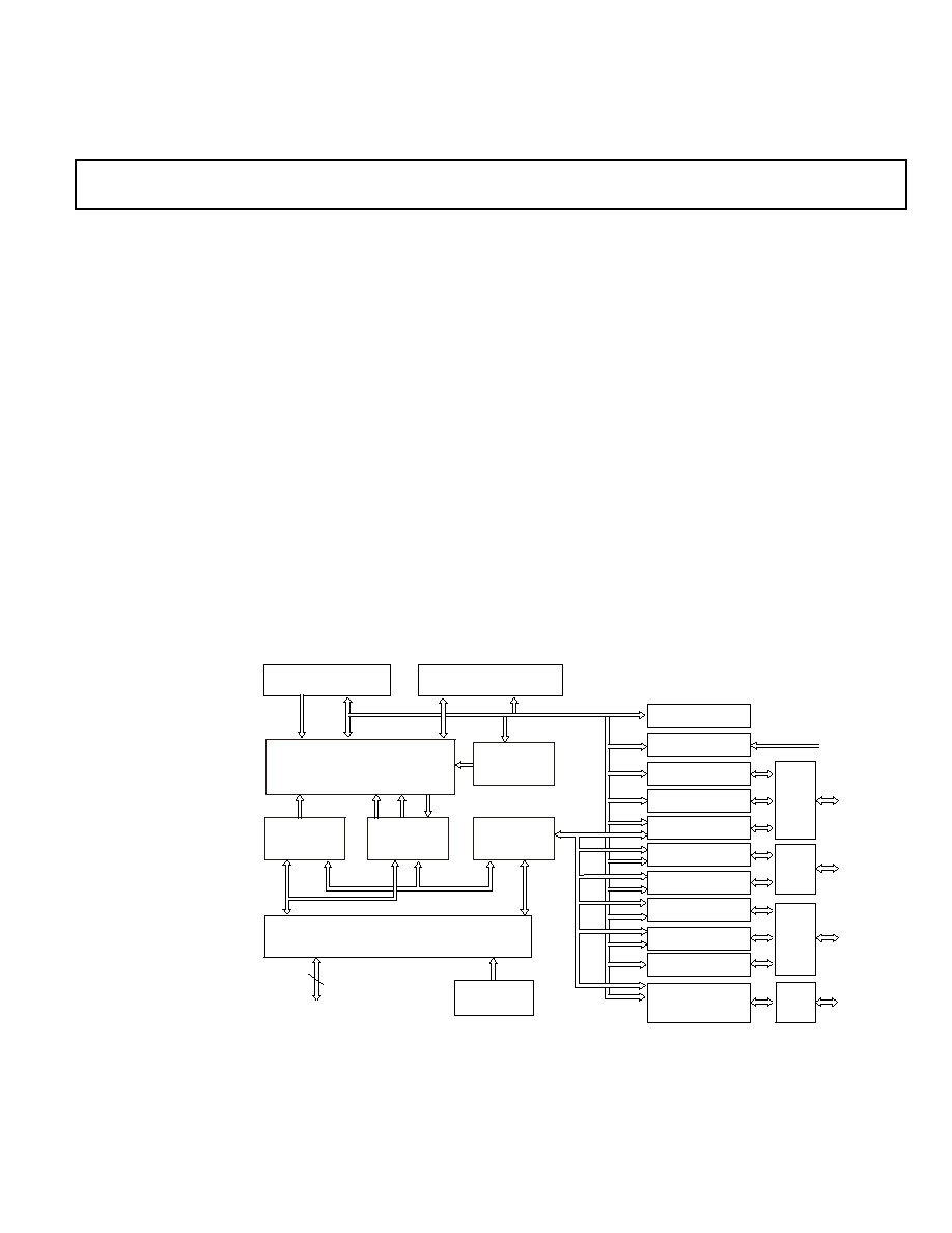
Figure 1. Functional Block Diagram
ETHERNET MAC
(ADSP-BF536/
BF537 ONLY)
TIMERS 0-7
UART 0-1
PPI
SPORT1
SPI
WATCHDOG TIMER
RTC
TWI
CAN
SPORT0
GPIO
PORT
F
GPIO
PORT
H
GPIO
PORT
G
PORT
J
EXTERNAL PORT
FLASH, SDRAM CONTROL
BOOT ROM
JTAG TEST AND EMULATION
VOLTAGE REGULATOR
DMA
CONTROLLER
L1
INSTRUCTION
MEMORY
L1
DATA
MEMORY
B
PERIPHERAL ACCESS BUS
D
M
A
A
C
C
E
S
S
B
U
S
EXTERNAL
ACCESS
BUS
DMA CORE BUS
D
M
A
E
X
T
E
R
N
A
L
B
U
S
P
E
R
I
P
H
E
R
A
L
A
C
C
E
S
S
B
U
S
16

Rev. B
|
Page 2 of 68
|
July 2006
ADSP-BF534/ADSP-BF536/ADSP-BF537
TABLE OF CONTENTS
General Description ................................................. 3
Portable Low Power Architecture ............................. 3
System Integration ................................................ 3
Blackfin Processor Peripherals ................................. 3
Blackfin Processor Core .......................................... 4
Memory Architecture ............................................ 5
DMA Controllers .................................................. 8
Real-Time Clock ................................................... 9
Watchdog Timer .................................................. 9
Timers ............................................................... 9
Serial Ports (SPORTs) .......................................... 10
Serial Peripheral Interface (SPI) Port ....................... 10
UART Ports ...................................................... 10
Controller Area Network (CAN) ............................ 11
TWI Controller Interface ...................................... 11
10/100 Ethernet MAC .......................................... 11
Ports ................................................................ 12
Parallel Peripheral Interface (PPI) ........................... 12
Dynamic Power Management ................................ 13
Voltage Regulation .............................................. 14
Clock Signals ..................................................... 14
Booting Modes ................................................... 16
Instruction Set Description ................................... 16
Development Tools ............................................. 17
Designing an Emulator-Compatible Processor Board .. 18
Related Documents ............................................. 18
Pin Descriptions .................................................... 19
Specifications ........................................................ 23
Operating Conditions .......................................... 23
Electrical Characteristics ....................................... 24
Absolute Maximum Ratings .................................. 25
ESD Sensitivity ................................................... 25
Package Information ............................................ 25
Timing Specifications ........................................... 26
Asynchronous Memory Read Cycle Timing ............ 28
Asynchronous Memory Write Cycle Timing ........... 29
External Port Bus Request and Grant Cycle Timing .. 30
SDRAM Interface Timing .................................. 31
External DMA Request Timing ............................ 32
Parallel Peripheral Interface Timing ...................... 33
Serial Ports ..................................................... 36
Serial Peripheral Interface Port--Master Timing ...... 40
Serial Peripheral Interface Port--Slave Timing ........ 41
Universal Asynchronous Receiver-Transmitter (UART)
Ports--Receive and Transmit Timing ................. 42
General-Purpose Port Timing ............................. 43
Timer Cycle Timing .......................................... 44
Timer Clock Timing ......................................... 45
JTAG Test and Emulation Port Timing .................. 46
10/100 Ethernet MAC Controller Timing ............... 47
Output Drive Currents ......................................... 50
Power Dissipation ............................................... 53
Test Conditions .................................................. 54
Capacitive Loading .............................................. 55
Thermal Characteristics ........................................ 58
182-Ball Mini-BGA Pinout ....................................... 59
208-Ball Sparse Mini-BGA Pinout .............................. 62
Outline Dimensions ................................................ 65
Surface Mount Design .......................................... 66
Ordering Guide ..................................................... 66
REVISION HISTORY
7/07--Revision B
For this revision of the data sheet, the ADSP-BF534,
ADSP-BF536, and ADSP-BF537 have been combined into
a single family data sheet. Because of this change, not all
processor features and attributes apply across all products. See
Table 1 on Page 3
for a breakdown of product offerings.
Added Table 10,
Maximum Duty Cycle for Input Transient
Voltage ............................................................. 25
Added
Universal Asynchronous Receiver-Transmitter (UART)
Ports--Receive and Transmit Timing ......................... 42
Revised
Figure 47
,
Figure 48
, and
Figure 49
Under
Test Conditions ..................................................... 54
Added 208-Ball Mini BGA
Thermal Characteristics on Page 58
and
208-Ball Sparse Mini-BGA Pinout on Page 62
.
ADSP-BF534/ADSP-BF536/ADSP-BF537
Rev. B
|
Page 3 of 68
|
July 2006
GENERAL DESCRIPTION
The ADSP-BF534/ADSP-BF536/ADSP-BF537 processors are
members of the Blackfin family of products, incorporating the
Analog Devices/Intel Micro Signal Architecture (MSA).
Blackfin processors combine a dual-MAC state-of-the-art signal
processing engine, the advantages of a clean, orthogonal RISC-
like microprocessor instruction set, and single-instruction,
multiple-data (SIMD) multimedia capabilities into a single
instruction-set architecture.
The ADSP-BF534/ADSP-BF536/ADSP-BF537 processors are
completely code and pin compatible. They differ only with
respect to their performance, on-chip memory, and presence of
the Ethernet MAC module. Specific performance, memory, and
feature configurations are shown in
Table 1
.
By integrating a rich set of industry-leading system peripherals
and memory, the Blackfin processors are the platform of choice
for next-generation applications that require RISC-like pro-
grammability, multimedia support, and leading-edge signal
processing in one integrated package.
PORTABLE LOW POWER ARCHITECTURE
Blackfin processors provide world-class power management
and performance. They are produced with a low power and low
voltage design methodology and feature on-chip dynamic
power management, which is the ability to vary both the voltage
and frequency of operation to significantly lower overall power
consumption. This capability can result in a substantial reduc-
tion in power consumption, compared with just varying the
frequency of operation. This allows longer battery life for
portable appliances.
SYSTEM INTEGRATION
The Blackfin processor is a highly integrated system-on-a-chip
solution for the next generation of embedded network-con-
nected applications. By combining industry-standard interfaces
with a high performance signal processing core, cost-effective
applications can be developed quickly, without the need for
costly external components. The system peripherals include an
IEEE-compliant 802.3 10/100 Ethernet MAC (ADSP-BF536 and
ADSP-BF537 only), a CAN 2.0B controller, a TWI controller,
two UART ports, an SPI port, two serial ports (SPORTs), nine
general-purpose 32-bit timers (eight with PWM capability), a
real-time clock, a watchdog timer, and a parallel peripheral
interface (PPI).
BLACKFIN PROCESSOR PERIPHERALS
The ADSP-BF534/ADSP-BF536/ADSP-BF537 processors con-
tains a rich set of peripherals connected to the core via several
high bandwidth buses, providing flexibility in system configura-
tion as well as excellent overall system performance (see the
block diagram
on Page 1
). The processors contain dedicated
network communication modules and high speed serial and
parallel ports, an interrupt controller for flexible management
of interrupts from the on-chip peripherals or external sources,
and power management control functions to tailor the perfor-
mance and power characteristics of the processor and system to
many application scenarios.
All of the peripherals, except for the general-purpose I/O, CAN,
TWI, real-time clock, and timers, are supported by a flexible
DMA structure. There are also separate memory DMA channels
dedicated to data transfers between the processor's various
memory spaces, including external SDRAM and asynchronous
memory. Multiple on-chip buses running at up to 133 MHz
provide enough bandwidth to keep the processor core running
along with activity on all of the on-chip and external
peripherals.
The Blackfin processors include an on-chip voltage regulator in
support of the processors' dynamic power management capabil-
ity. The voltage regulator provides a range of core voltage levels
when supplied from a single 2.25 V to 3.6 V input. The voltage
regulator can be bypassed at the user's discretion.
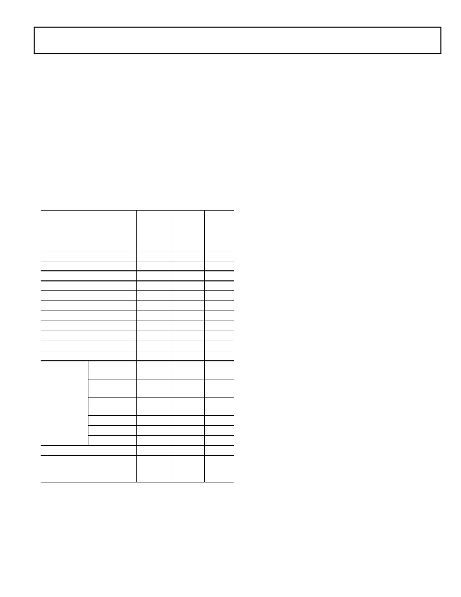
Table 1. Processor Comparison
Features
ADSP
-
BF534
ADSP
-
BF536
ADSP
-
BF537
Ethernet MAC
--
1
1
CAN 1
1
1
TWI
1
1
1
SPORTs
2
2
2
UARTs
2
2
2
SPI 1
1
1
GP Timers
8
8
8
Watchdog Timers
1
1
1
RTC
1
1
1
Parallel Peripheral Interface
1
1
1
GPIOs
48 48 48
Memory
Configuration
L1 Instruction
SRAM/Cache
16K bytes
16K bytes 16K bytes
L1 Instruction
SRAM
48K bytes
48K bytes 48K bytes
L1 Data
SRAM/Cache
32K bytes
32K bytes 32K bytes
L1 Data SRAM
32K bytes
--
32K bytes
L1 Scratchpad
4K bytes
4K bytes
4K bytes
L3 Boot ROM
2K bytes
2K bytes
2K bytes
Maximum Speed Grade
500 MHz
400 MHz
600 MHz
Package Options:
Sparse Mini-BGA
Mini-BGA
208-Ball
182-Ball
208-Ball
182-Ball
208-Ball
182-Ball
Rev. B
|
Page 4 of 68
|
July 2006
ADSP-BF534/ADSP-BF536/ADSP-BF537
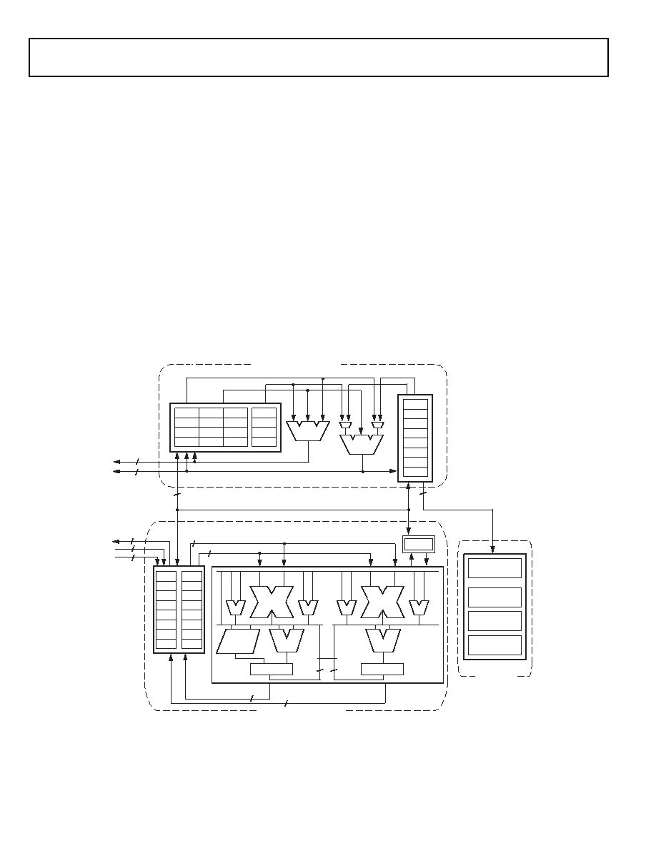
BLACKFIN PROCESSOR CORE
As shown in
Figure 2 on Page 4
, the Blackfin processor core
contains two 16-bit multipliers, two 40-bit accumulators, two
40-bit ALUs, four video ALUs, and a 40-bit shifter. The compu-
tation units process 8-, 16-, or 32-bit data from the register file.
The compute register file contains eight 32-bit registers. When
performing compute operations on 16-bit operand data, the
register file operates as 16 independent 16-bit registers. All
operands for compute operations come from the multiported
register file and instruction constant fields.
Each MAC can perform a 16-bit by 16-bit multiply in each
cycle, accumulating the results into the 40-bit accumulators.
Signed and unsigned formats, rounding, and saturation
are supported.
The ALUs perform a traditional set of arithmetic and logical
operations on 16-bit or 32-bit data. In addition, many special
instructions are included to accelerate various signal processing
tasks. These include bit operations such as field extract and pop-
ulation count, modulo 2
32
multiply, divide primitives, saturation
and rounding, and sign/exponent detection. The set of video
instructions include byte alignment and packing operations,
16-bit and 8-bit adds with clipping, 8-bit average operations,
and 8-bit subtract/absolute value/accumulate (SAA) operations.
Also provided are the compare/select and vector search
instructions.
For certain instructions, two 16-bit ALU operations can be per-
formed simultaneously on register pairs (a 16-bit high half and
16-bit low half of a compute register). If the second ALU is used,
quad 16-bit operations are possible.
The 40-bit shifter can perform shifts and rotates and is used to
support normalization, field extract, and field deposit
instructions.
The program sequencer controls the flow of instruction execu-
tion, including instruction alignment and decoding. For
program flow control, the sequencer supports PC relative and
indirect conditional jumps (with static branch prediction), and
subroutine calls. Hardware is provided to support zero-over-
head looping. The architecture is fully interlocked, meaning that
the programmer need not manage the pipeline when executing
instructions with data dependencies.
Figure 2. Blackfin Processor Core
SEQUENCER
ALIGN
DECODE
LOOP BUFFER
16
16
8
8
8
8
40
40
A0
A1
BARREL
SHIFTER
DATA ARITHMETIC UNIT
CONTROL
UNIT
R7.H
R6.H
R5.H
R4.H
R3.H
R2.H
R1.H
R0.H
R7.L
R6.L
R5.L
R4.L
R3.L
R2.L
R1.H
R0.L
ASTAT
40 40
32
32
32
32
32
32
32
LD0
LD1
SD
DAG0
DAG1
ADDRESS ARITHMETIC UNIT
I3
I2
I1
I0
L3
L2
L1
L0
B3
B2
B1
B0
M3
M2
M1
M0
SP
FP
P5
P4
P3
P2
P1
P0
DA1
DA0
32
32
32
PREG
RAB
32
TO
MEMORY

ADSP-BF534/ADSP-BF536/ADSP-BF537
Rev. B
|
Page 5 of 68
|
July 2006
The address arithmetic unit provides two addresses for simulta-
neous dual fetches from memory. It contains a multiported
register file consisting of four sets of 32-bit index, modify,
length, and base registers (for circular buffering), and eight
additional 32-bit pointer registers (for C-style indexed stack
manipulation).
Blackfin processors support a modified Harvard architecture in
combination with a hierarchical memory structure. Level 1 (L1)
memories are those that typically operate at the full processor
speed with little or no latency. At the L1 level, the instruction
memory holds instructions only. The two data memories hold
data, and a dedicated scratchpad data memory stores stack and
local variable information.
In addition, multiple L1 memory blocks are provided, offering a
configurable mix of SRAM and cache. The memory manage-
ment unit (MMU) provides memory protection for individual
tasks that may be operating on the core and can protect system
registers from unintended access.
The architecture provides three modes of operation: user mode,
supervisor mode, and emulation mode. User mode has
restricted access to certain system resources, thus providing a
protected software environment, while supervisor mode has
unrestricted access to the system and core resources.
The Blackfin processor instruction set has been optimized so
that 16-bit opcodes represent the most frequently used instruc-
tions, resulting in excellent compiled code density. Complex
DSP instructions are encoded into 32-bit opcodes, representing
fully featured multifunction instructions. Blackfin processors
support a limited multi-issue capability, where a 32-bit instruc-
tion can be issued in parallel with two 16-bit instructions,
allowing the programmer to use many of the core resources in a
single instruction cycle.
The Blackfin processor assembly language uses an algebraic syn-
tax for ease of coding and readability. The architecture has been
optimized for use in conjunction with the C/C++ compiler,
resulting in fast and efficient software implementations.
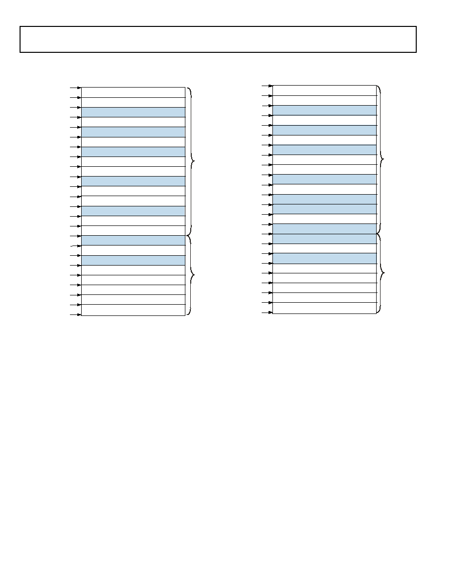
MEMORY ARCHITECTURE
The ADSP-BF534/ADSP-BF536/ADSP-BF537 processors view
memory as a single unified 4G byte address space, using 32-bit
addresses. All resources, including internal memory, external
memory, and I/O control registers, occupy separate sections of
this common address space. The memory portions of this
address space are arranged in a hierarchical structure to provide
a good cost/performance balance of some very fast, low latency
on-chip memory as cache or SRAM, and larger, lower cost, and
performance off-chip memory systems. See
Figure 3
.
The on-chip L1 memory system is the highest performance
memory available to the Blackfin processor. The off-chip mem-
ory system, accessed through the external bus interface unit
(EBIU), provides expansion with SDRAM, flash memory, and
SRAM, optionally accessing up to 516M bytes of
physical memory.
The memory DMA controller provides high bandwidth data-
movement capability. It can perform block transfers of code or
data between the internal memory and the external
memory spaces.
Internal (On-Chip) Memory
The ADSP-BF534/ADSP-BF536/ADSP-BF537 processors have
three blocks of on-chip memory providing high-bandwidth
access to the core.
The first block is the L1 instruction memory, consisting of
64K bytes SRAM, of which 16K bytes can be configured as a
four-way set-associative cache. This memory is accessed at full
processor speed.
The second on-chip memory block is the L1 data memory, con-
sisting of up to two banks of up to 32K bytes each. Each memory
bank is configurable, offering both cache and SRAM functional-
ity. This memory block is accessed at full processor speed.
The third memory block is a 4K byte scratchpad SRAM, which
runs at the same speed as the L1 memories, but is only accessible
as data SRAM, and cannot be configured as cache memory.
External (Off-Chip) Memory
External memory is accessed via the EBIU. This 16-bit interface
provides a glueless connection to a bank of synchronous DRAM
(SDRAM) as well as up to four banks of asynchronous memory
devices including flash, EPROM, ROM, SRAM, and memory
mapped I/O devices.
The PC133-compliant SDRAM controller can be programmed
to interface to up to 512M bytes of SDRAM. A separate row can
be open for each SDRAM internal bank, and the SDRAM con-
troller supports up to 4 internal SDRAM banks, improving
overall performance.
The asynchronous memory controller can be programmed to
control up to four banks of devices with very flexible timing
parameters for a wide variety of devices. Each bank occupies a
1M byte segment regardless of the size of the devices used, so
that these banks are only contiguous if each is fully populated
with 1M byte of memory.
I/O Memory Space
The ADSP-BF534/ADSP-BF536/ADSP-BF537 processors do
not define a separate I/O space. All resources are mapped
through the flat 32-bit address space. On-chip I/O devices have
their control registers mapped into memory-mapped registers
(MMRs) at addresses near the top of the 4G byte address space.
These are separated into two smaller blocks, one which contains
the control MMRs for all core functions, and the other which
contains the registers needed for setup and control of the on-
chip peripherals outside of the core. The MMRs are accessible
only in supervisor mode and appear as reserved space to on-
chip peripherals.
Rev. B
|
Page 6 of 68
|
July 2006
ADSP-BF534/ADSP-BF536/ADSP-BF537
Booting
The Blackfin processor contains a small on-chip boot kernel,
which configures the appropriate peripheral for booting. If the
Blackfin processor is configured to boot from boot ROM mem-
ory space, the processor starts executing from the on-chip boot
ROM. For more information, see
Booting Modes on Page 16
.
Event Handling
The event controller on the Blackfin processor handles all asyn-
chronous and synchronous events to the processor. The
Blackfin processor provides event handling that supports both
nesting and prioritization. Nesting allows multiple event service
routines to be active simultaneously. Prioritization ensures that
servicing of a higher priority event takes precedence over servic-
ing of a lower priority event. The controller provides support for
five different types of events:
· Emulation An emulation event causes the processor to
enter emulation mode, allowing command and control of
the processor via the JTAG interface.
· Reset This event resets the processor.
· Nonmaskable Interrupt (NMI) The NMI event can be
generated by the software watchdog timer or by the NMI
input signal to the processor. The NMI event is frequently
used as a power-down indicator to initiate an orderly shut-
down of the system.
· Exceptions Events that occur synchronously to program
flow (in other words, the exception is taken before the
instruction is allowed to complete). Conditions such as
data alignment violations and undefined instructions cause
exceptions.
· Interrupts Events that occur asynchronously to program
flow. They are caused by input pins, timers, and other
peripherals, as well as by an explicit software instruction.
Each event type has an associated register to hold the return
address and an associated return-from-event instruction. When
an event is triggered, the state of the processor is saved on the
supervisor stack.
The Blackfin processor event controller consists of two stages,
the core event controller (CEC) and the system interrupt con-
troller (SIC). The core event controller works with the system
interrupt controller to prioritize and control all system events.
Figure 3. ADSP-BF534/ADSP-BF536/ADSP-BF537 Memory Maps
RESERVED
CORE MMR REGISTERS (2M BYTES)
RESERVED
SCRATCHPAD SRAM (4K BYTES)
INSTRUCTION BANK B SRAM (16K BYTES)
SYSTEM MMR REGISTERS (2M BYTES)
RESERVED
RESERVED
DATA BANK B SRAM/CACHE (16K BYTES)
DATA BANK B SRAM (16K BYTES)
DATA BANK A SRAM/CACHE (16K BYTES)
ASYNC MEMORY BANK 3 (1M BYTES)
ASYNC MEMORY BANK 2 (1M BYTES)
ASYNC MEMORY BANK 1 (1M BYTES)
ASYNC MEMORY BANK 0 (1M BYTES)
SDRAM MEMORY (16M BYTES TO 512M BYTES)
INSTRUCTION SRAM/CACHE (16K BYTES)
I
N
T
E
R
N
A
L
M
E
M
O
R
Y
M
A
P
E
X
T
E
R
N
A
L
M
E
M
O
R
Y
M
A
P
0xFFFF FFFF
0xFFE0 0000
0xFFB0 0000
0xFFA1 4000
0xFFA1 0000
0xFF90 8000
0xFF90 4000
0xFF80 8000
0xFF80 4000
0x2040 0000
0x2030 0000
0x2020 0000
0x2010 0000
0x2000 0000
0xEF00 0000
0x0000 0000
0xFFC0 0000
0xFFB0 1000
0xFFA0 0000
DATA BANK A SRAM (16K BYTES)
0xFF90 0000
0xFF80 0000
RESERVED
RESERVED
0xFFA0 C000
0xFFA0 8000
INSTRUCTION BANK A SRAM (32K BYTES)
RESERVED
BOOT ROM (2K BYTES)
0xEF00 0800
ADSP-BF534/ADSP-BF537 MEMORY MAP
RESERVED
CORE MMR REGISTERS (2M BYTES)
RESERVED
SCRATCHPAD SRAM (4K BYTES)
INSTRUCTION BANK B SRAM (16K BYTES)
SYSTEM MMR REGISTERS (2M BYTES)
RESERVED
RESERVED
DATA BANK B SRAM/CACHE (16K BYTES)
DATA BANK A SRAM/CACHE (16K BYTES)
ASYNC MEMORY BANK 3 (1M BYTES)
ASYNC MEMORY BANK 2 (1M BYTES)
ASYNC MEMORY BANK 1 (1M BYTES)
ASYNC MEMORY BANK 0 (1M BYTES)
SDRAM MEMORY (16M BYTES TO 512M BYTES)
INSTRUCTION SRAM/CACHE (16K BYTES)
I
N
T
E
R
N
A
L
M
E
M
O
R
Y
M
A
P
E
X
T
E
R
N
A
L
M
E
M
O
R
Y
M
A
P
0xFFFF FFFF
0xFFE0 0000
0xFFB0 0000
0xFFA1 4000
0xFFA1 0000
0xFF90 8000
0xFF90 4000
0xFF80 8000
0xFF80 4000
0x2040 0000
0x2030 0000
0x2020 0000
0x2010 0000
0x2000 0000
0xEF00 0000
0x0000 0000
0xFFC0 0000
0xFFB0 1000
0xFFA0 0000
0xFF90 0000
0xFF80 0000
RESERVED
RESERVED
0xFFA0 C000
0xFFA0 8000
INSTRUCTION BANK A SRAM (32K BYTES)
RESERVED
RESERVED
RESERVED
BOOT ROM (2K BYTES)
0xEF00 0800
ADSP-BF536 MEMORY MAP

ADSP-BF534/ADSP-BF536/ADSP-BF537
Rev. B
|
Page 7 of 68
|
July 2006
Conceptually, interrupts from the peripherals enter into the
SIC, and are then routed directly into the general-purpose inter-
rupts of the CEC.
Core Event Controller (CEC)
The CEC supports nine general-purpose interrupts (IVG157),
in addition to the dedicated interrupt and exception events. Of
these general-purpose interrupts, the two lowest priority
interrupts (IVG1514) are recommended to be reserved for
software interrupt handlers, leaving seven prioritized interrupt
inputs to support the peripherals of the Blackfin processor.
Table 2
describes the inputs to the CEC, identifies their names
in the event vector table (EVT), and lists their priorities.
System Interrupt Controller (SIC)
The system interrupt controller provides the mapping and rout-
ing of events from the many peripheral interrupt sources to the
prioritized general-purpose interrupt inputs of the CEC.
Although the processor provides a default mapping, the user
can alter the mappings and priorities of interrupt events by writ-
ing the appropriate values into the interrupt assignment
registers (IAR).
Table 3
describes the inputs into the SIC and the
default mappings into the CEC.
Table 2. Core Event Controller (CEC)
Priority
(0 Is Highest)
Event Class
EVT Entry
0
Emulation/Test Control
EMU
1
Reset
RST
2
Nonmaskable Interrupt
NMI
3
Exception
EVX
4
Reserved
--
5
Hardware Error
IVHW
6
Core Timer
IVTMR
7
General-Purpose Interrupt 7
IVG7
8
General-Purpose Interrupt 8
IVG8
9
General-Purpose Interrupt 9
IVG9
10
General-Purpose Interrupt 10
IVG10
11
General-Purpose Interrupt 11
IVG11
12
General-Purpose Interrupt 12
IVG12
13
General-Purpose Interrupt 13
IVG13
14
General-Purpose Interrupt 14
IVG14
15
General-Purpose Interrupt 15
IVG15
Table 3. System Interrupt Controller (SIC)
Peripheral Interrupt Event
Default
Mapping
Peripheral
Interrupt ID
PLL Wakeup
IVG7
0
DMA Error (generic)
IVG7
1
DMAR0 Block Interrupt
IVG7
1
DMAR1 Block Interrupt
IVG7
1
DMAR0 Overflow Error
IVG7
1
DMAR1 Overflow Error
IVG7
1
CAN Error
IVG7
2
Ethernet Error (ADSP-BF536 and
ADSP-BF537 only)
IVG7
2
SPORT 0 Error
IVG7
2
SPORT 1 Error
IVG7
2
PPI Error
IVG7
2
SPI Error
IVG7
2
UART0 Error
IVG7
2
UART1 Error
IVG7
2
Real-Time Clock
IVG8
3
DMA Channel 0 (PPI)
IVG8
4
DMA Channel 3 (SPORT 0 Rx)
IVG9
5
DMA Channel 4 (SPORT 0 Tx)
IVG9
6
DMA Channel 5 (SPORT 1 Rx)
IVG9
7
DMA Channel 6 (SPORT 1 Tx)
IVG9
8
TWI
IVG10
9
DMA Channel 7 (SPI)
IVG10
10
DMA Channel 8 (UART0 Rx)
IVG10
11
DMA Channel 9 (UART0 Tx)
IVG10
12
DMA Channel 10 (UART1 Rx)
IVG10
13
DMA Channel 11 (UART1 Tx)
IVG10
14
CAN Rx
IVG11
15
CAN Tx
IVG11
16
DMA Channel 1 (Ethernet Rx,
ADSP-BF536 and ADSP-BF537 only)
IVG11
17
Port H Interrupt A
IVG11
17
DMA Channel 2 (Ethernet Tx,
ADSP-BF536 and ADSP-BF537 only)
IVG11
18
Port H Interrupt B
IVG11
18
Timer 0
IVG12
19
Timer 1
IVG12
20
Timer 2
IVG12
21
Timer 3
IVG12
22
Timer 4
IVG12
23
Timer 5
IVG12
24
Timer 6
IVG12
25
Timer 7
IVG12
26
Port F, G Interrupt A
IVG12
27
Port G Interrupt B
IVG12
28

Rev. B
|
Page 8 of 68
|
July 2006
ADSP-BF534/ADSP-BF536/ADSP-BF537
Event Control
The Blackfin processor provides a very flexible mechanism to
control the processing of events. In the CEC, three registers are
used to coordinate and control events. Each register is
16 bits wide:
· CEC interrupt latch register (ILAT) Indicates when
events have been latched. The appropriate bit is set when
the processor has latched the event and cleared when the
event has been accepted into the system. This register is
updated automatically by the controller, but it may be writ-
ten only when its corresponding IMASK bit is cleared.
· CEC interrupt mask register (IMASK) Controls the
masking and unmasking of individual events. When a bit is
set in the IMASK register, that event is unmasked and is
processed by the CEC when asserted. A cleared bit in the
IMASK register masks the event, preventing the processor
from servicing the event even though the event may be
latched in the ILAT register. This register may be read or
written while in supervisor mode. (Note that general-pur-
pose interrupts can be globally enabled and disabled with
the STI and CLI instructions, respectively.)
· CEC interrupt pending register (IPEND) The IPEND
register keeps track of all nested events. A set bit in the
IPEND register indicates the event is currently active or
nested at some level. This register is updated automatically
by the controller but may be read while in supervisor mode.
The SIC allows further control of event processing by providing
three 32-bit interrupt control and status registers. Each register
contains a bit corresponding to each of the peripheral interrupt
events shown in
Table 3 on Page 7
.
· SIC interrupt mask register (SIC_IMASK) Controls the
masking and unmasking of each peripheral interrupt event.
When a bit is set in the register, that peripheral event is
unmasked and is processed by the system when asserted. A
cleared bit in the register masks the peripheral event, pre-
venting the processor from servicing the event.
· SIC interrupt status register (SIC_ISR) As multiple
peripherals can be mapped to a single event, this register
allows the software to determine which peripheral event
source triggered the interrupt. A set bit indicates the
peripheral is asserting the interrupt, and a cleared bit indi-
cates the peripheral is not asserting the event.
· SIC interrupt wakeup enable register (SIC_IWR) By
enabling the corresponding bit in this register, a peripheral
can be configured to wake up the processor, should the
core be idled when the event is generated. (
For more infor-
mation, see Dynamic Power Management on Page 13.
)
Because multiple interrupt sources can map to a single general-
purpose interrupt, multiple pulse assertions can occur simulta-
neously, before or during interrupt processing for an interrupt
event already detected on this interrupt input. The IPEND reg-
ister contents are monitored by the SIC as the interrupt
acknowledgement.
The appropriate ILAT register bit is set when an interrupt rising
edge is detected (detection requires two core clock cycles). The
bit is cleared when the respective IPEND register bit is set. The
IPEND bit indicates that the event has entered into the proces-
sor pipeline. At this point the CEC recognizes and queues the
next rising edge event on the corresponding event input. The
minimum latency from the rising edge transition of the general-
purpose interrupt to the IPEND output asserted is three core
clock cycles; however, the latency can be much higher, depend-
ing on the activity within and the state of the processor.
DMA CONTROLLERS
The Blackfin processors have multiple, independent DMA con-
trollers that support automated data transfers with minimal
overhead for the processor core. DMA transfers can occur
between the processor's internal memories and any of its DMA-
capable peripherals. Additionally, DMA transfers can be accom-
plished between any of the DMA-capable peripherals and
external devices connected to the external memory interfaces,
including the SDRAM controller and the asynchronous mem-
ory controller. DMA-capable peripherals include the Ethernet
MAC (ADSP-BF536 and ADSP-BF537 only), SPORTs, SPI port,
UARTs, and PPI. Each individual DMA-capable peripheral has
at least one dedicated DMA channel.
The DMA controller supports both one-dimensional (1-D) and
two-dimensional (2-D) DMA transfers. DMA transfer initial-
ization can be implemented from registers or from sets of
parameters called descriptor blocks.
The 2-D DMA capability supports arbitrary row and column
sizes up to 64K elements by 64K elements, and arbitrary row
and column step sizes up to ±32K elements. Furthermore, the
column step size can be less than the row step size, allowing
implementation of interleaved data streams. This feature is
especially useful in video applications where data can be de-
interleaved on the fly.
Examples of DMA types supported by the DMA controller
include:
· A single, linear buffer that stops upon completion
· A circular, auto-refreshing buffer that interrupts on each
full or fractionally full buffer
· 1-D or 2-D DMA using a linked list of descriptors
· 2-D DMA using an array of descriptors, specifying only the
base DMA address within a common page.
DMA Channels 12 and 13
(Memory DMA Stream 0)
IVG13
29
DMA Channels 14 and 15
(Memory DMA Stream 1)
IVG13
30
Software Watchdog Timer
IVG13
31
Port F Interrupt B
IVG13
31
Table 3. System Interrupt Controller (SIC) (Continued)
Peripheral Interrupt Event
Default
Mapping
Peripheral
Interrupt ID

ADSP-BF534/ADSP-BF536/ADSP-BF537
Rev. B
|
Page 9 of 68
|
July 2006
In addition to the dedicated peripheral DMA channels, there are
two memory DMA channels provided for transfers between the
various memories of the processor system. This enables trans-
fers of blocks of data between any of the memories--including
external SDRAM, ROM, SRAM, and flash memory--with mini-
mal processor intervention. Memory DMA transfers can be
controlled by a very flexible descriptor-based methodology or
by a standard register-based autobuffer mechanism.
The ADSP-BF534/ADSP-BF536/ADSP-BF537 processors also
have an external DMA controller capability via dual external
DMA request pins when used in conjunction with the external
bus interface unit (EBIU). This functionality can be used when a
high speed interface is required for external FIFOs and high
bandwidth communications peripherals such as USB 2.0. It
allows control of the number of data transfers for memDMA.
The number of transfers per edge is programmable. This feature
can be programmed to allow memDMA to have an increased
priority on the external bus relative to the core.
REAL-TIME CLOCK
The real-time clock (RTC) provides a robust set of digital watch
features, including current time, stopwatch, and alarm. The
RTC is clocked by a 32.768 kHz crystal external to the
processor. The RTC peripheral has dedicated power supply pins
so that it can remain powered up and clocked even when the
rest of the processor is in a low-power state. The RTC provides
several programmable interrupt options, including interrupt
per second, minute, hour, or day clock ticks, interrupt on pro-
grammable stopwatch countdown, or interrupt at a
programmed alarm time.
The 32.768 kHz input clock frequency is divided down to a 1 Hz
signal by a prescaler. The counter function of the timer consists
of four counters: a 60-second counter, a 60-minute counter, a
24-hour counter, and an 32,768-day counter.
When enabled, the alarm function generates an interrupt when
the output of the timer matches the programmed value in the
alarm control register. There are two alarms: The first alarm is
for a time of day, while the second alarm is for a day and time of
that day.
The stopwatch function counts down from a programmed
value, with one-second resolution. When the stopwatch is
enabled and the counter underflows, an interrupt is generated.
Like the other peripherals, the RTC can wake up the processor
from sleep mode upon generation of any RTC wakeup event.
Additionally, an RTC wakeup event can wake up the processor
from deep sleep mode, and wake up the on-chip internal voltage
regulator from the hibernate operating mode.
Connect RTC pins RTXI and RTXO with external components
as shown in
Figure 4
.
WATCHDOG TIMER
The ADSP-BF534/ADSP-BF536/ADSP-BF537 processors
include a 32-bit timer that can be used to implement a software
watchdog function. A software watchdog can improve system
availability by forcing the processor to a known state through
generation of a hardware reset, nonmaskable interrupt (NMI),
or general-purpose interrupt, if the timer expires before being
reset by software. The programmer initializes the count value of
the timer, enables the appropriate interrupt, then enables the
timer. Thereafter, the software must reload the counter before it
counts to zero from the programmed value. This protects the
system from remaining in an unknown state where software,
which would normally reset the timer, has stopped running due
to an external noise condition or software error.
If configured to generate a hardware reset, the watchdog timer
resets both the core and the processor peripherals. After a reset,
software can determine if the watchdog was the source of the
hardware reset by interrogating a status bit in the watchdog
timer control register.
The timer is clocked by the system clock (SCLK), at a maximum
frequency of f
SCLK
.
TIMERS
There are nine general-purpose programmable timer units in
the processor. Eight timers have an external pin that can be con-
figured either as a pulse width modulator (PWM) or timer
output, as an input to clock the timer, or as a mechanism for
measuring pulse widths and periods of external events. These
timers can be synchronized to an external clock input to the sev-
eral other associated PF pins, to an external clock input to the
PPI_CLK input pin, or to the internal SCLK.
The timer units can be used in conjunction with the two UARTs
and the CAN controller to measure the width of the pulses in
the data stream to provide a software auto-baud detect function
for the respective serial channels.
The timers can generate interrupts to the processor core provid-
ing periodic events for synchronization, either to the system
clock or to a count of external signals.
In addition to the eight general-purpose programmable timers,
a ninth timer is also provided. This extra timer is clocked by the
internal processor clock and is typically used as a system tick
clock for generating periodic interrupts in an operating system.
Figure 4. External Components for RTC
RTXO
C1
C2
X1
SUGGESTED COMPONENTS:
ECLIPTEK EC38J (THROUGH-HOLE PACKAGE)
EPSON MC405 12pF LOAD (SURFACE MOUNT PACKAGE)
C1 = 22pF
C2 = 22pF
R1 = 10M
YSTAL SPECIFIED FOR X1.
CONTACT CRYSTAL MANUFACTURER FOR DETAILS. C1 AND C2
SPECIFICATIONS ASSUME BOARD TRACE CAPACITANCE OF 3pF.
RTXI
R1

Rev. B
|
Page 10 of 68
|
July 2006
ADSP-BF534/ADSP-BF536/ADSP-BF537
SERIAL PORTS (SPORTs)
The ADSP-BF534/ADSP-BF536/ADSP-BF537 processors
incorporate two dual-channel synchronous serial ports
(SPORT0 and SPORT1) for serial and multiprocessor commu-
nications. The SPORTs support the following features:
· I
2
S capable operation.
· Bidirectional operation Each SPORT has two sets of inde-
pendent transmit and receive pins, enabling eight channels
of I
2
S stereo audio.
· Buffered (8-deep) transmit and receive ports Each port
has a data register for transferring data words to and from
other processor components and shift registers for shifting
data in and out of the data registers.
· Clocking Each transmit and receive port can either use an
external serial clock or generate its own, in frequencies
ranging from (f
SCLK
/131,070) Hz to (f
SCLK
/2) Hz.
· Word length Each SPORT supports serial data words
from 3 to 32 bits in length, transferred most significant bit
first or least significant bit first.
· Framing Each transmit and receive port can run with or
without frame sync signals for each data word. Frame sync
signals can be generated internally or externally, active high
or low, and with either of two pulse widths and early or late
frame sync.
· Companding in hardware Each SPORT can perform
A-law or -law companding according to ITU recommen-
dation G.711. Companding can be selected on the transmit
and/or receive channel of the SPORT without
additional latencies.
· DMA operations with single-cycle overhead Each SPORT
can automatically receive and transmit multiple buffers of
memory data. The processor can link or chain sequences of
DMA transfers between a SPORT and memory.
· Interrupts Each transmit and receive port generates an
interrupt upon completing the transfer of a data word or
after transferring an entire data buffer, or buffers,
through DMA.
· Multichannel capability Each SPORT supports 128 chan-
nels out of a 1024-channel window and is compatible with
the H.100, H.110, MVIP-90, and HMVIP standards.
SERIAL PERIPHERAL INTERFACE (SPI) PORT
The ADSP-BF534/ADSP-BF536/ADSP-BF537 processors have
an SPI-compatible port that enables the processor to communi-
cate with multiple SPI-compatible devices.
The SPI interface uses three pins for transferring data: two data
pins (Master Output-Slave Input, MOSI, and Master Input-
Slave Output, MISO) and a clock pin (serial clock, SCK). An SPI
chip select input pin (SPISS) lets other SPI devices select the
processor, and seven SPI chip select output pins (SPISEL71) let
the processor select other SPI devices. The SPI select pins are
reconfigured programmable flag pins. Using these pins, the SPI
port provides a full-duplex, synchronous serial interface, which
supports both master/slave modes and multimaster
environments.
The SPI port's baud rate and clock phase/polarities are pro-
grammable, and it has an integrated DMA controller,
configurable to support transmit or receive data streams. The
SPI's DMA controller can only service unidirectional accesses at
any given time.
The SPI port's clock rate is calculated as:
Where the 16-bit SPI_Baud register contains a value of 2
to 65,535.
During transfers, the SPI port simultaneously transmits and
receives by serially shifting data in and out on its two serial data
lines. The serial clock line synchronizes the shifting and sam-
pling of data on the two serial data lines.
UART PORTS
The ADSP-BF534/ADSP-BF536/ADSP-BF537 processors pro-
vide two full-duplex universal asynchronous receiver and
transmitter (UART) ports, which are fully compatible with PC-
standard UARTs. Each UART port provides a simplified UART
interface to other peripherals or hosts, supporting full-duplex,
DMA-supported, asynchronous transfers of serial data. A
UART port includes support for five to eight data bits, one or
two stop bits, and none, even, or odd parity. Each UART port
supports two modes of operation:
· PIO (programmed I/O) The processor sends or receives
data by writing or reading I/O mapped UART registers.
The data is double-buffered on both transmit and receive.
· DMA (direct memory access) The DMA controller trans-
fers both transmit and receive data. This reduces the
number and frequency of interrupts required to transfer
data to and from memory. The UART has two dedicated
DMA channels, one for transmit and one for receive. These
DMA channels have lower default priority than most DMA
channels because of their relatively low service rates.
Each UART port's baud rate, serial data format, error code gen-
eration and status, and interrupts are programmable:
· Supporting bit rates ranging from (f
SCLK
/1,048,576) to
(f
SCLK
/16) bits per second.
· Supporting data formats from 7 to 12 bits per frame.
· Both transmit and receive operations can be configured to
generate maskable interrupts to the processor.
The UART port's clock rate is calculated as:
Where the 16-bit UARTx_Divisor comes from the DLH register
(most significant 8 bits) and UARTx_DLL register (least signifi-
cant 8 bits).
SPI Clock Rate
f
SCLK
2
SPI_Baud
×
--------------------------------
=
UART Clock Rate
f
SCLK
16
UART_Divisor
×
-----------------------------------------------
=

ADSP-BF534/ADSP-BF536/ADSP-BF537
Rev. B
|
Page 11 of 68
|
July 2006
In conjunction with the general-purpose timer functions, auto-
baud detection is supported.
The capabilities of the UARTs are further extended with sup-
port for the infrared data association (IrDA) serial infrared
physical layer link specification (SIR) protocol.
CONTROLLER AREA NETWORK (CAN)
The ADSP-BF534/ADSP-BF536/ADSP-BF537 processors offer
a CAN controller that is a communication controller imple-
menting the CAN 2.0B (active) protocol. This protocol is an
asynchronous communications protocol used in both industrial
and automotive control systems. The CAN protocol is well-
suited for control applications due to its capability to communi-
cate reliably over a network, since the protocol incorporates
CRC checking message error tracking, and fault node
confinement.
The CAN controller offers the following features:
· 32 mailboxes (eight receive only, eight transmit only, 16
configurable for receive or transmit).
· Dedicated acceptance masks for each mailbox.
· Additional data filtering on first two bytes.
· Support for both the standard (11-bit) and extended
(29-bit) identifier (ID) message formats.
· Support for remote frames.
· Active or passive network support.
· CAN wakeup from hibernation mode (lowest static power
consumption mode).
· Interrupts, including: Tx complete, Rx complete, error,
global.
The electrical characteristics of each network connection are
very demanding so the CAN interface is typically divided into
two parts: a controller and a transceiver. This allows a single
controller to support different drivers and CAN networks. The
CAN module represents only the controller part of the interface.
The controller interface supports connection to 3.3 V high-
speed, fault-tolerant, single-wire transceivers.
TWI CONTROLLER INTERFACE
The ADSP-BF534/ADSP-BF536/ADSP-BF537 processors
include a 2-wire interface (TWI) module for providing a simple
exchange method of control data between multiple devices. The
TWI is compatible with the widely used I
2
C
®
bus standard. The
TWI module offers the capabilities of simultaneous master and
slave operation, support for both 7-bit addressing and multime-
dia data arbitration. The TWI interface utilizes two pins for
transferring clock (SCL) and data (SDA) and supports the
protocol at speeds up to 400k bits/sec. The TWI interface pins
are compatible with 5 V logic levels.
Additionally, the processor's TWI module is fully compatible
with serial camera control bus (SCCB) functionality for easier
control of various CMOS camera sensor devices.
10/100 ETHERNET MAC
The ADSP-BF536 and ADSP-BF537 processors offer the capa-
bility to directly connect to a network by way of an embedded
Fast Ethernet Media Access Controller (MAC) that supports
both 10-BaseT (10M bits/sec) and 100-BaseT (100M bits/sec)
operation. The 10/100 Ethernet MAC peripheral is fully compli-
ant to the IEEE 802.3-2002 standard, and it provides
programmable features designed to minimize supervision, bus
use, or message processing by the rest of the processor system.
Some standard features are:
· Support of MII and RMII protocols for external PHYs.
· Full duplex and half duplex modes.
· Data framing and encapsulation: generation and detection
of preamble, length padding, and FCS.
· Media access management (in half-duplex operation): col-
lision and contention handling, including control of
retransmission of collision frames and of back-off timing.
· Flow control (in full-duplex operation): generation and
detection of PAUSE frames.
· Station management: generation of MDC/MDIO frames
for read-write access to PHY registers.
· SCLK operating range down to 25 MHz (active and sleep
operating modes).
· Internal loopback from Tx to Rx.
Some advanced features are:
· Buffered crystal output to external PHY for support of a
single crystal system.
· Automatic checksum computation of IP header and IP
payload fields of Rx frames.
· Independent 32-bit descriptor-driven Rx and Tx DMA
channels.
· Frame status delivery to memory via DMA, including
frame completion semaphores, for efficient buffer queue
management in software.
· Tx DMA support for separate descriptors for MAC header
and payload to eliminate buffer copy operations.
· Convenient frame alignment modes support even 32-bit
alignment of encapsulated Rx or Tx IP packet data in mem-
ory after the 14-byte MAC header.
· Programmable Ethernet event interrupt supports any com-
bination of:
· Any selected Rx or Tx frame status conditions.
· PHY interrupt condition.
· Wakeup frame detected.
· Any selected MAC management counter(s) at
half-full.
· DMA descriptor error.
· 47 MAC management statistics counters with selectable
clear-on-read behavior and programmable interrupts on
half maximum value.

Rev. B
|
Page 12 of 68
|
July 2006
ADSP-BF534/ADSP-BF536/ADSP-BF537
· Programmable Rx address filters, including a 64-bit
address hash table for multicast and/or unicast frames, and
programmable filter modes for broadcast, multicast, uni-
cast, control, and damaged frames.
· Advanced power management supporting unattended
transfer of Rx and Tx frames and status to/from external
memory via DMA during low-power sleep mode.
· System wakeup from sleep operating mode upon magic
packet or any of four user-definable wakeup frame filters.
· Support for 802.3Q tagged VLAN frames.
· Programmable MDC clock rate and preamble suppression.
· In RMII operation, 7 unused pins may be configured as
GPIO pins for other purposes.
PORTS
The ADSP-BF534/ADSP-BF536/ADSP-BF537 processors
group the many peripheral signals to four ports--Port F, Port G,
Port H, and Port J. Most of the associated pins are shared by
multiple signals. The ports function as multiplexer controls.
Eight of the pins (Port F70) offer high source/high sink current
capabilities.
General-Purpose I/O (GPIO)
The processors have 48 bidirectional, general-purpose I/O
(GPIO) pins allocated across three separate GPIO modules--
PORTFIO, PORTGIO, and PORTHIO, associated with Port F,
Port G, and Port H, respectively. Port J does not provide GPIO
functionality. Each GPIO-capable pin shares functionality with
other processor peripherals via a multiplexing scheme; however,
the GPIO functionality is the default state of the device upon
power-up. Neither GPIO output or input drivers are active by
default. Each general-purpose port pin can be individually con-
trolled by manipulation of the port control, status, and interrupt
registers:
· GPIO direction control register Specifies the direction of
each individual GPIO pin as input or output.
· GPIO control and status registers The processors employ
a "write one to modify" mechanism that allows any combi-
nation of individual GPIO pins to be modified in a single
instruction, without affecting the level of any other GPIO
pins. Four control registers are provided. One register is
written in order to set pin values, one register is written in
order to clear pin values, one register is written in order to
toggle pin values, and one register is written in order to
specify a pin value. Reading the GPIO status register allows
software to interrogate the sense of the pins.
· GPIO interrupt mask registers The two GPIO interrupt
mask registers allow each individual GPIO pin to function
as an interrupt to the processor. Similar to the two GPIO
control registers that are used to set and clear individual
pin values, one GPIO interrupt mask register sets bits to
enable interrupt function, and the other GPIO interrupt
mask register clears bits to disable interrupt function.
GPIO pins defined as inputs can be configured to generate
hardware interrupts, while output pins can be triggered by
software interrupts.
· GPIO interrupt sensitivity registers The two GPIO inter-
rupt sensitivity registers specify whether individual pins are
level- or edge-sensitive and specify--if edge-sensitive--
whether just the rising edge or both the rising and falling
edges of the signal are significant. One register selects the
type of sensitivity, and one register selects which edges are
significant for edge-sensitivity.
PARALLEL PERIPHERAL INTERFACE (PPI)
The ADSP-BF534/ADSP-BF536/ADSP-BF537 processors pro-
vide a parallel peripheral interface (PPI) that can connect
directly to parallel A/D and D/A converters, ITU-R-601/656
video encoders and decoders, and other general-purpose
peripherals. The PPI consists of a dedicated input clock pin, up
to 3 frame synchronization pins, and up to 16 data pins.
In ITU-R-656 modes, the PPI receives and parses a data stream
of 8-bit or 10-bit data elements. On-chip decode of embedded
preamble control and synchronization information
is supported.
Three distinct ITU-R-656 modes are supported:
· Active video only mode The PPI does not read in any
data between the End of Active Video (EAV) and Start of
Active Video (SAV) preamble symbols, or any data present
during the vertical blanking intervals. In this mode, the
control byte sequences are not stored to memory; they are
filtered by the PPI.
· Vertical blanking only mode The PPI only transfers verti-
cal blanking interval (VBI) data, as well as horizontal
blanking information and control byte sequences on
VBI lines.
· Entire field mode The entire incoming bitstream is read
in through the PPI. This includes active video, control pre-
amble sequences, and ancillary data that may be embedded
in horizontal and vertical blanking intervals.
Though not explicitly supported, ITU-R-656 output functional-
ity can be achieved by setting up the entire frame structure
(including active video, blanking, and control information) in
memory and streaming the data out the PPI in a frame sync-less
mode. The processor's 2-D DMA features facilitate this transfer
by allowing the static frame buffer (blanking and control codes)
to be placed in memory once, and simply updating the active
video information on a per-frame basis.
The general-purpose modes of the PPI are intended to suit a
wide variety of data capture and transmission applications. The
modes are divided into four main categories, each allowing up
to 16 bits of data transfer per PPI_CLK cycle:
· Data receive with internally generated frame syncs
· Data receive with externally generated frame syncs
· Data transmit with internally generated frame syncs
· Data transmit with externally generated frame syncs

ADSP-BF534/ADSP-BF536/ADSP-BF537
Rev. B
|
Page 13 of 68
|
July 2006
These modes support ADC/DAC connections, as well as video
communication with hardware signalling. Many of the modes
support more than one level of frame synchronization. If
desired, a programmable delay can be inserted between asser-
tion of a frame sync and reception/transmission of data.
DYNAMIC POWER MANAGEMENT
The ADSP-BF534/ADSP-BF536/ADSP-BF537 processors pro-
vide five operating modes, each with a different performance
and power profile. In addition, dynamic power management
provides the control functions to dynamically alter the proces-
sor core supply voltage, further reducing power dissipation.
Control of clocking to each of the peripherals also reduces
power consumption. See
Table 4
for a summary of the power
settings for each mode.
Full-On Operating Mode--Maximum Performance
In the full-on mode, the PLL is enabled and is not bypassed,
providing capability for maximum operational frequency. This
is the power-up default execution state in which maximum per-
formance can be achieved. The processor core and all enabled
peripherals run at full speed.
Active Operating Mode--Moderate Power Savings
In the active mode, the PLL is enabled but bypassed. Because the
PLL is bypassed, the processor's core clock (CCLK) and system
clock (SCLK) run at the input clock (CLKIN) frequency. In this
mode, the CLKIN to CCLK multiplier ratio can be changed,
although the changes are not realized until the full-on mode is
entered. DMA access is available to appropriately configured
L1 memories.
In the active mode, it is possible to disable the PLL through the
PLL control register (PLL_CTL). If disabled, the PLL must be
re-enabled before transitioning to the full-on or sleep modes.
Sleep Operating Mode--High Dynamic Power Savings
The sleep mode reduces dynamic power dissipation by disabling
the clock to the processor core (CCLK). The PLL and system
clock (SCLK), however, continue to operate in this mode. Typi-
cally an external event or RTC activity wakes up the processor.
When in the sleep mode, asserting wakeup causes the processor
to sense the value of the BYPASS bit in the PLL control register
(PLL_CTL). If BYPASS is disabled, the processor transitions to
the full on mode. If BYPASS is enabled, the processor transi-
tions to the active mode.
System DMA access to L1 memory is not supported in
sleep mode.
Deep Sleep Operating Mode--Maximum Dynamic Power
Savings
The deep sleep mode maximizes dynamic power savings by dis-
abling the clocks to the processor core (CCLK) and to all
synchronous peripherals (SCLK). Asynchronous peripherals,
such as the RTC, may still be running but cannot access internal
resources or external memory. This powered-down mode can
only be exited by assertion of the reset interrupt (RESET) or by
an asynchronous interrupt generated by the RTC. When in deep
sleep mode, an RTC asynchronous interrupt causes the proces-
sor to transition to the active mode. Assertion of RESET while
in deep sleep mode causes the processor to transition to the full-
on mode.
Hibernate Operating Mode--Maximum Static Power
Savings
The hibernate mode maximizes static power savings by dis-
abling the voltage and clocks to the processor core (CCLK) and
to all of the synchronous peripherals (SCLK). The internal volt-
age regulator for the processor can be shut off by writing b#00 to
the FREQ bits of the VR_CTL register. This disables both CCLK
and SCLK. Furthermore, it sets the internal power supply volt-
age (V
DDINT
) to 0 V to provide the greatest power savings. To
preserve the processor state, prior to removing power, any criti-
cal information stored internally (memory contents, register
contents, etc.) must be written to a non volatile storage device.
Since V
DDEXT
is still supplied in this mode, all of the external pins
three-state, unless otherwise specified. This allows other devices
that are connected to the processor to still have power applied
without drawing unwanted current.
The Ethernet or CAN modules can wake up the internal supply
regulator. The regulator can also be woken up by a real-time
clock wakeup event or by asserting the RESET pin, both of
which initiate the hardware reset sequence.
With the exception of the VR_CTL and the RTC registers, all
internal registers and memories lose their content in the hiber-
nate state. State variables may be held in external SRAM or
SDRAM. The CKELOW bit in the VR_CTL register controls
whether SDRAM operates in self-refresh mode which allows it
to retain its content while the processor is in reset.
Power Savings
As shown in
Table 5
, the processors support three different
power domains which maximizes flexibility, while maintaining
compliance with industry standards and conventions. By isolat-
ing the internal logic of the processor into its own power
domain, separate from the RTC and other I/O, the processor
can take advantage of dynamic power management, without
affecting the RTC or other I/O devices. There are no sequencing
requirements for the various power domains.
Table 4. Power Settings
Mode
PLL
PLL
Bypassed
Core
Clock
(CCLK)
System
Clock
(SCLK)
Internal
Power
(VDDINT)
Full On
Enabled
No
Enabled
Enabled
On
Active
Enabled/
Disabled
Yes
Enabled
Enabled
On
Sleep
Enabled
--
Disabled
Enabled
On
Deep Sleep
Disabled
--
Disabled
Disabled
On
Hibernate
Disabled
--
Disabled
Disabled
Off
Rev. B
|
Page 14 of 68
|
July 2006
ADSP-BF534/ADSP-BF536/ADSP-BF537
The dynamic power management feature allows both the pro-
cessor's input voltage (V
DDINT
) and clock frequency (f
CCLK
) to be
dynamically controlled.
The power dissipated by a processor is largely a function of its
clock frequency and the square of the operating voltage. For
example, reducing the clock frequency by 25% results in a 25%
reduction in power dissipation, while reducing the voltage by
25% reduces power dissipation by more than 40%. Further,
these power savings are additive, in that if the clock frequency
and supply voltage are both reduced, the power savings can be
dramatic, as shown in the following equations.
The power savings factor is calculated as:
where the variables in the equations are:
f
CCLKNOM
is the nominal core clock frequency
f
CCLKRED
is the reduced core clock frequency
V
DDINTNOM
is the nominal internal supply voltage
V
DDINTRED
is the reduced internal supply voltage
T
NOM
is the duration running at f
CCLKNOM
T
RED
is the duration running at f
CCLKRED
The percent power savings is calculated as:
VOLTAGE REGULATION
The ADSP-BF534/ADSP-BF536/ADSP-BF537 processor pro-
vides an on-chip voltage regulator that can generate processor
core voltage levels (0.85 V to 1.2 V guaranteed from 5% to
+10%) from an external 2.25 V to 3.6 V supply.
Figure 5
shows
the typical external components required to complete the power
management system. The regulator controls the internal logic
voltage levels and is programmable with the voltage regulator
control register (VR_CTL) in increments of 50 mV. To reduce
standby power consumption, the internal voltage regulator can
be programmed to remove power to the processor core while
keeping I/O power supplied. While in hibernate mode, V
DDEXT
can still be applied, eliminating the need for external buffers.
The voltage regulator can be activated from this power-down
state by asserting the RESET pin, which then initiates a boot
sequence. The regulator can also be disabled and bypassed at the
user's discretion.
CLOCK SIGNALS
The ADSP-BF534/ADSP-BF536/ADSP-BF537 processor can be
clocked by an external crystal, a sine wave input, or a buffered,
shaped clock derived from an external clock oscillator.
If an external clock is used, it should be a TTL compatible signal
and must not be halted, changed, or operated below the speci-
fied frequency during normal operation. This signal is
connected to the processor's CLKIN pin. When an external
clock is used, the XTAL pin must be left unconnected.
Alternatively, because the processors include an on-chip oscilla-
tor circuit, an external crystal may be used. For fundamental
frequency operation, use the circuit shown in
Figure 6
. A
parallel-resonant, fundamental frequency, microprocessor-
grade crystal is connected across the CLKIN and XTAL pins.
The on-chip resistance between CLKIN and the XTAL pin is in
the 500 k
range. Further parallel resistors are typically not rec-
ommended. The two capacitors and the series resistor shown in
Figure 6
fine-tune phase and amplitude of the sine frequency.
The capacitor and resistor values shown in
Figure 6
are typical
values only. The capacitor values are dependent upon the crystal
manufacturers' load capacitance recommendations and the PCB
physical layout. The resistor value depends on the drive level
specified by the crystal manufacturer. The user should verify the
customized values based on careful investigations of multiple
devices over temperature range.
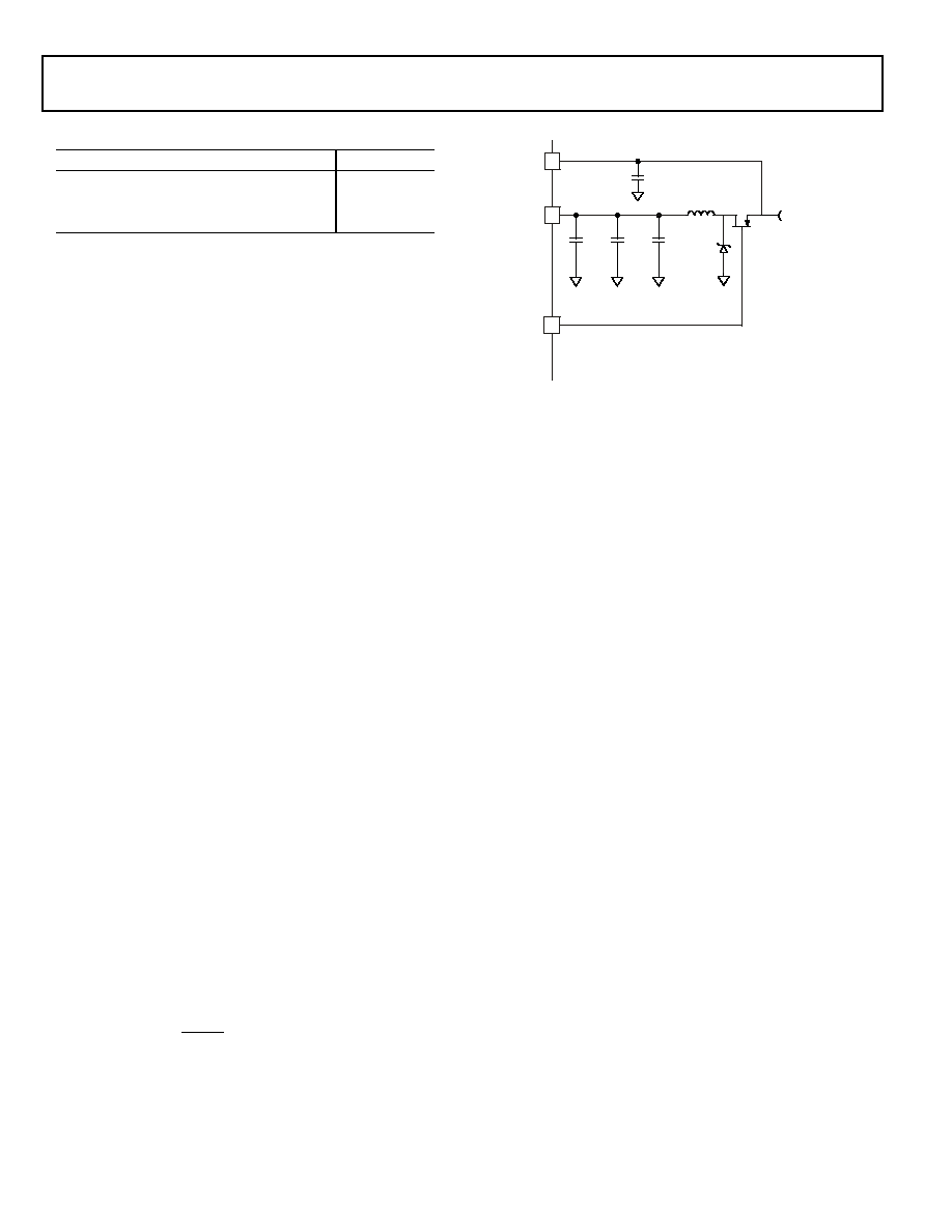
A third-overtone crystal can be used for frequencies above
25 MHz. The circuit is then modified to ensure crystal operation
only at the third overtone, by adding a tuned inductor circuit as
shown in
Figure 6
. A design procedure for third-overtone oper-
ation is discussed in detail in application note EE-168.
The CLKBUF pin is an output pin, and is a buffer version of the
input clock. This pin is particularly useful in Ethernet applica-
tions to limit the number of required clock sources in the
system. In this type of application, a single 25 MHz or 50 MHz
crystal may be applied directly to the processors. The 25 MHz or
50 MHz output of CLKBUF can then be connected to an exter-
nal Ethernet MII or RMII PHY device.
Table 5. Power Domains
Power Domain
V
DD
Range
All internal logic, except RTC
V
DDINT
RTC internal logic and crystal I/O
V
DDRTC
All other I/O
V
DDEXT
power savings factor
f
CCLKRED
f
CCLKNOM
---------------------
V
DDINTRED
V
DDINTNOM
--------------------------
2
×
T
RED
T
NOM
-------------
×
=
% power savings
1
power savings factor
(
)
100%
×
=
Figure 5. Voltage Regulator Circuit
V
DDEXT
V
DDINT
VR
OUT
1-0
EXTERNAL COMPONENTS
2.25V TO 3.6V
INPUT VOLTAGE
RANGE
NDS8434
ZHCS1000
100µF
1µF
10µH
0.1µF
NOTE: VR
OUT
1-0 SHOULD BE TIED TOGETHER EXTERNALLY
AND DESIGNER SHOULD MINIMIZE TRACE LENGTH TO NDS8434.
100µF
ADSP-BF534/ADSP-BF536/ADSP-BF537
Rev. B
|
Page 15 of 68
|
July 2006
Because of the default 10x PLL multiplier, providing a 50 MHz
CLKIN exceeds the recommended operating conditions of the
lower speed grades. Because of this restriction, a 50 MHz RMII
PHY cannot be clocked directly from the CLKBUF pin. Either
provide a separate 50 MHz clock source, or use an RMII PHY
with 25 MHz clock input options. The CLKBUF output is active
by default and can be disabled using the VR_CTL register for
power savings.
The Blackfin core runs at a different clock rate than the on-chip
peripherals. As shown in
Figure 7
, the core clock (CCLK) and
system peripheral clock (SCLK) are derived from the input
clock (CLKIN) signal. An on-chip PLL is capable of multiplying
the CLKIN signal by a programmable 0.5
×
to 64
×
multiplication
factor (bounded by specified minimum and maximum VCO
frequencies). The default multiplier is 10
×
, but it can be modi-
fied by a software instruction sequence in the PLL_CTL register.
On-the-fly CCLK and SCLK frequency changes can be effected
by simply writing to the PLL_DIV register. Whereas the maxi-
mum allowed CCLK and SCLK rates depend on the applied
voltages V
DDINT
and V
DDEXT
, the VCO is always permitted to run
up to the frequency specified by the part's speed grade. The
CLKOUT pin reflects the SCLK frequency to the off-chip world.
It belongs to the SDRAM interface, but it functions as reference
signal in other timing specifications as well. While active by
default, it can be disabled using the EBIU_SDGCTL and
EBIU_AMGCTL registers.
All on-chip peripherals are clocked by the system clock (SCLK).
The system clock frequency is programmable by means of the
SSEL30 bits of the PLL_DIV register. The values programmed
into the SSEL fields define a divide ratio between the PLL output
(VCO) and the system clock. SCLK divider values are 1 through
15.
Table 6
illustrates typical system clock ratios.
Note that the divisor ratio must be chosen to limit the system
clock frequency to its maximum of f
SCLK
. The SSEL value can be
changed dynamically without any PLL lock latencies by writing
the appropriate values to the PLL divisor register (PLL_DIV).
The core clock (CCLK) frequency can also be dynamically
changed by means of the CSEL10 bits of the PLL_DIV register.
Supported CCLK divider ratios are 1, 2, 4, and 8, as shown in
Table 7
. This programmable core clock capability is useful for
fast core frequency modifications.
The maximum CCLK frequency not only depends on the part's
speed grade (see
Ordering Guide on Page 66
), it also depends on
the applied V
DDINT
voltage. See
Table 12
and
Table 13
for details.
The maximal system clock rate (SCLK) depends on the chip
package and the applied V
DDEXT
voltage (see
Table 16
).
Figure 6. External Crystal Connections
CLKIN
CLKOUT
XTAL
EN
CLKBUF
TO PLL CIRCUITRY
FOR OVERTONE
OPERATION ONLY:
NOTE: VALUES MARKED WITH * MUST BE CUSTOMIZED
DEPENDING ON THE CRYSTAL AND LAYOUT. PLEASE
ANALYZE CAREFULLY.
18pF*
EN
18pF*
330 *
BLACKFIN
Figure 7. Frequency Modification Methods
Table 6. Example System Clock Ratios
Signal Name
SSEL30
Divider Ratio
VCO/SCLK
Example Frequency Ratios
(MHz)
VCO
SCLK
0001
1:1
100
100
0110
6:1
300
50
1010
10:1
500
50
Table 7. Core Clock Ratios
Signal Name
CSEL10
Divider Ratio
VCO/CCLK
Example Frequency Ratios
(MHz)
VCO
CCLK
00
1:1
300
300
01
2:1
300
150
10
4:1
500
125
11
8:1
200
25
PLL
0.5
- 64
1 TO 15
1, 2, 4, 8
VCO
CLKI N
"FINE" ADJUSTMENT
REQUIRES PLL SEQUENCING
"COURSE" ADJUSTMENT
ON THE FLY
CCLK
SCLK
SCLK
CCLK
SCLK
133MHz

Rev. B
|
Page 16 of 68
|
July 2006
ADSP-BF534/ADSP-BF536/ADSP-BF537
BOOTING MODES
The ADSP-BF534/ADSP-BF536/ADSP-BF537 processor has six
mechanisms (listed in
Table 8
) for automatically loading inter-
nal and external memory after a reset. A seventh mode is
provided to execute from external memory, bypassing the boot
sequence.
The BMODE pins of the reset configuration register, sampled
during power-on resets and software-initiated resets, imple-
ment the following modes:
· Execute from 16-bit external memory Execution starts
from address 0x2000 0000 with 16-bit packing. The boot
ROM is bypassed in this mode. All configuration settings
are set for the slowest device possible (3-cycle hold time;
15-cycle R/W access times; 4-cycle setup).
· Boot from 8-bit and 16-bit external flash memory The
8-bit or 16-bit flash boot routine located in Boot ROM
memory space is set up using asynchronous memory bank
0. All configuration settings are set for the slowest device
possible (3-cycle hold time; 15-cycle R/W access times;
4-cycle setup). The Boot ROM evaluates the first byte of the
boot stream at address 0x2000 0000. If it is 0x40, 8-bit boot
is performed. A 0x60 byte assumes a 16-bit memory device
and performs 8-bit DMA. A 0x20 byte also assumes 16-bit
memory but performs 16-bit DMA.
· Boot from serial SPI memory (EEPROM or flash) 8-, 16-,
or 24-bit addressable devices are supported as well as
AT45DB041, AT45DB081, AT45DB161, AT45DB321,
AT45DB642, and AT45DB1282 DataFlash
®
devices from
Atmel. The SPI uses the PF10/SPI SSEL1 output pin to
select a single SPI EEPROM/flash device, submits a read
command and successive address bytes (0x00) until a valid
8-, 16-, or 24-bit, or Atmel addressable device is detected,
and begins clocking data into the processor.
· Boot from SPI host device The Blackfin processor oper-
ates in SPI slave mode and is configured to receive the bytes
of the .LDR file from an SPI host (master) agent. To hold
off the host device from transmitting while the boot ROM
is busy, the Blackfin processor asserts a GPIO pin, called
host wait (HWAIT), to signal the host device not to send
any more bytes until the flag is deasserted. The flag is cho-
sen by the user and this information is transferred to the
Blackfin processor via bits 10:5 of the FLAG header.
· Boot from UART Using an autobaud handshake
sequence, a boot-stream-formatted program is downloaded
by the host. The host agent selects a baud rate within the
UART's clocking capabilities. When performing the auto-
baud, the UART expects an "@" (boot stream) character
(8 bits data, 1 start bit, 1 stop bit, no parity bit) on the RXD
pin to determine the bit rate. It then replies with an
acknowledgement that is composed of 4 bytes: 0xBF, the
value of UART_DLL, the value of UART_DLH, and 0x00.
The host can then download the boot stream. When the
processor needs to hold off the host, it deasserts CTS.
Therefore, the host must monitor this signal.
· Boot from serial TWI memory (EEPROM/flash) The
Blackfin processor operates in master mode and selects the
TWI slave with the unique ID 0xA0. It submits successive
read commands to the memory device starting at two byte
internal address 0x0000 and begins clocking data into the
processor. The TWI memory device should comply with
Philips I
2
C Bus Specification version 2.1 and have the capa-
bility to auto-increment its internal address counter such
that the contents of the memory device can be read
sequentially.
· Boot from TWI host The TWI host agent selects the slave
with the unique ID 0x5F. The processor replies with an
acknowledgement and the host can then download the
boot stream. The TWI host agent should comply with
Philips I
2
C Bus Specification version 2.1. An I
2
C multi-
plexer can be used to select one processor at a time when
booting multiple processors from a single TWI.
For each of the boot modes, a 10-byte header is first brought in
from an external device. The header specifies the number of
bytes to be transferred and the memory destination address.
Multiple memory blocks may be loaded by any boot sequence.
Once all blocks are loaded, program execution commences from
the start of L1 instruction SRAM.
In addition, Bit 4 of the reset configuration register can be set by
application code to bypass the normal boot sequence during a
software reset. For this case, the processor jumps directly to the
beginning of L1 instruction memory.
To augment the boot modes, a secondary software loader can be
added to provide additional booting mechanisms. This second-
ary loader could provide the capability to boot from flash,
variable baud rate, and other sources. In all boot modes except
bypass, program execution starts from on-chip L1 memory
address 0xFFA0 0000.
INSTRUCTION SET DESCRIPTION
The Blackfin processor family assembly language instruction set
employs an algebraic syntax designed for ease of coding and
readability. The instructions have been specifically tuned to pro-
vide a flexible, densely encoded instruction set that compiles to
a very small final memory size. The instruction set also provides
fully featured multifunction instructions that allow the
Table 8. Booting Modes
BMODE2 0
Description
000
Execute from 16-bit external memory (bypass
boot ROM)
001
Boot from 8-bit or 16-bit memory
(EPROM/flash)
010
Reserved
011
Boot from serial SPI memory (EEPROM/flash)
100
Boot from SPI host (slave mode)
101
Boot from serial TWI memory (EEPROM/flash)
110
Boot from TWI host (slave mode)
111
Boot from UART host (slave mode)

ADSP-BF534/ADSP-BF536/ADSP-BF537
Rev. B
|
Page 17 of 68
|
July 2006
programmer to use many of the processor core resources in a
single instruction. Coupled with many features more often seen
on microcontrollers, this instruction set is very efficient when
compiling C and C++ source code. In addition, the architecture
supports both user (algorithm/application code) and supervisor
(O/S kernel, device drivers, debuggers, ISRs) modes of opera-
tion, allowing multiple levels of access to core processor
resources.
The assembly language, which takes advantage of the proces-
sor's unique architecture, offers the following advantages:
· Seamlessly integrated DSP/MCU features are optimized for
both 8-bit and 16-bit operations.
· A multi-issue load/store modified-Harvard architecture,
which supports two 16-bit MAC or four 8-bit ALU + two
load/store + two pointer updates per cycle.
· All registers, I/O, and memory are mapped into a unified
4G byte memory space, providing a simplified program-
ming model.
· Microcontroller features, such as arbitrary bit and bit-field
manipulation, insertion, and extraction; integer operations
on 8-, 16-, and 32-bit data-types; and separate user and
supervisor stack pointers.
· Code density enhancements, which include intermixing of
16-bit and 32-bit instructions (no mode switching, no code
segregation). Frequently used instructions are encoded
in 16 bits.
DEVELOPMENT TOOLS
The Blackfin is supported with a complete set of
CROSSCORE
®
software and hardware development tools,
including Analog Devices emulators and the VisualDSP++
®
development environment. The same emulator hardware that
supports other Analog Devices processors also fully emulates
the Blackfin.
The VisualDSP++ project management environment lets pro-
grammers develop and debug an application. This environment
includes an easy to use assembler that is based on an algebraic
syntax, an archiver (librarian/library builder), a linker, a loader,
a cycle-accurate instruction-level simulator, a C/C++ compiler,
and a C/C++ runtime library that includes DSP and mathemati-
cal functions. A key point for these tools is C/C++ code
efficiency. The compiler has been developed for efficient
translation of C/C++ code to Blackfin assembly. The Blackfin
processor has architectural features that improve the efficiency
of compiled C/C++ code.
The VisualDSP++ debugger has a number of important fea-
tures. Data visualization is enhanced by a plotting package that
offers a significant level of flexibility. This graphical representa-
tion of user data enables the programmer to quickly determine
the performance of an algorithm. As algorithms grow in com-
plexity, this capability can have increasing significance on the
designer's development schedule, increasing productivity. Sta-
tistical profiling enables the programmer to nonintrusively poll
the processor as it is running the program. This feature, unique
to VisualDSP++, enables the software developer to passively
gather important code execution metrics without interrupting
the real-time characteristics of the program. Essentially, the
developer can identify bottlenecks in software quickly and effi-
ciently. By using the profiler, the programmer can focus on
those areas in the program that impact performance and take
corrective action.
Debugging both C/C++ and assembly programs with the
VisualDSP++ debugger, programmers can:
· View mixed C/C++ and assembly code (interleaved source
and object information).
· Insert breakpoints.
· Set conditional breakpoints on registers, memory, and
stacks.
· Trace instruction execution.
· Perform linear or statistical profiling of program execution.
· Fill, dump, and graphically plot the contents of memory.
· Perform source level debugging.
· Create custom debugger windows.
The VisualDSP++ IDE lets programmers define and manage
software development. Its dialog boxes and property pages let
programmers configure and manage all development tools,
including color syntax highlighting in the VisualDSP++ editor.
These capabilities permit programmers to:
· Control how the development tools process inputs and
generate outputs.
· Maintain a one-to-one correspondence with the tool's
command line switches.
The VisualDSP++ Kernel (VDK) incorporates scheduling and
resource management tailored specifically to address the mem-
ory and timing constraints of embedded, real-time
programming. These capabilities enable engineers to develop
code more effectively, eliminating the need to start from the
very beginning when developing new application code. The
VDK features include threads, critical and unscheduled regions,
semaphores, events, and device flags. The VDK also supports
priority-based, pre-emptive, cooperative, and time-sliced sched-
uling approaches. In addition, the VDK was designed to be
scalable. If the application does not use a specific feature, the
support code for that feature is excluded from the target system.
Because the VDK is a library, a developer can decide whether to
use it or not. The VDK is integrated into the VisualDSP++
development environment, but can also be used with standard
command line tools. When the VDK is used, the development
environment assists the developer with many error prone tasks
and assists in managing system resources, automating the gen-
eration of various VDK-based objects, and visualizing the
system state when debugging an application that uses the VDK.
CROSSCORE is a registered trademark of Analog Devices, Inc.
VisualDSP++ is a registered trademark of Analog Devices, Inc.

Rev. B
|
Page 18 of 68
|
July 2006
ADSP-BF534/ADSP-BF536/ADSP-BF537
VCSE is Analog Devices' technology for creating, using, and
reusing software components (independent modules of sub-
stantial functionality) to quickly and reliably assemble software
applications. Components can be downloaded from the Web
and dropped into the application. Component archives can be
published from within VisualDSP++. VCSE supports compo-
nent implementation in C/C++ or assembly language.
The expert linker can be used to visually manipulate the place-
ment of code and data in the embedded system. Memory
utilization can be viewed in a color-coded graphical form. Code
and data can be easily moved to different areas of the processor
or external memory with the drag of the mouse. Runtime stack
and heap usage can be examined. The expert linker is fully com-
patible with existing linker definition file (LDF), allowing the
developer to move between the graphical and textual
environments.
Analog Devices emulators use the IEEE 1149.1 JTAG test access
port of the Blackfin to monitor and control the target board
processor during emulation. The emulator provides full-speed
emulation, allowing inspection and modification of memory,
registers, and processor stacks. Nonintrusive in-circuit emula-
tion is assured by the use of the processor's JTAG interface--the
emulator does not affect target system loading or timing.
In addition to the software and hardware development tools
available from Analog Devices, third parties provide a wide
range of tools supporting the Blackfin processor family. Third
party software tools include DSP libraries, real-time operating
systems, and block diagram design tools.
EZ-KIT Lite® Evaluation Board
For evaluation of ADSP-BF534/ADSP-BF536/ADSP-BF537
processors, use the ADSP-BF537 EZ-KIT Lite board available
from Analog Devices. Order part number ADDS-BF537-
EZLITE. The board comes with on-chip emulation capabilities
and is equipped to enable software development. Multiple
daughter cards are available.
DESIGNING AN EMULATOR-COMPATIBLE
PROCESSOR BOARD
The Analog Devices family of emulators are tools that every sys-
tem developer needs in order to test and debug hardware and
software systems. Analog Devices has supplied an IEEE 1149.1
JTAG Test Access Port (TAP) on each JTAG processor. The
emulator uses the TAP to access the internal features of the pro-
cessor, allowing the developer to load code, set breakpoints,
observe variables, observe memory, and examine registers. The
processor must be halted to send data and commands, but once
an operation has been completed by the emulator, the processor
system is set running at full speed with no impact on
system timing.
To use these emulators, the target board must include a header
that connects the processor's JTAG port to the emulator.
For details on target board design issues including mechanical
layout, single processor connections, multiprocessor scan
chains, signal buffering, signal termination, and emulator pod
logic, see Analog Devices JTAG Emulation Technical Reference
(EE-68) on the Analog Devices website under
www.analog.com/ee-notes
. This document is updated regularly
to keep pace with improvements to emulator support.
RELATED DOCUMENTS
The following publications that describe the ADSP-BF534/
ADSP-BF536/ADSP-BF537 processors (and related processors)
can be ordered from any Analog Devices sales office or accessed
electronically on our website:
· Getting Started with Blackfin Processors
· ADSP-BF537 Blackfin Processor Hardware Reference
· ADSP-BF53x/ADSP-BF56x Blackfin Processor Program-
ming Reference
· ADSP-BF537 Blackfin Processor Anomaly List

ADSP-BF534/ADSP-BF536/ADSP-BF537
Rev. B
|
Page 19 of 68
|
July 2006
PIN DESCRIPTIONS
ADSP-BF534/ADSP-BF536/ADSP-BF537 processor's pin defi-
nitions are listed in
Table 9
. In order to maintain maximum
function and reduce package size and pin count, some pins have
dual, multiplexed functions. In cases where pin function is
reconfigurable, the default state is shown in plain text, while the
alternate function is shown in italics. Pins shown with an aster-
isk after their name (*) offer high source/high sink current
capabilities.
All pins are three-stated during and immediately after reset,
with the exception of the external memory interface and the
buffered XTAL output pin (CLKBUF). On the external memory
interface, the control and address lines are driven high during
reset unless the BR pin is asserted.
All I/O pins have their input buffers disabled with the exception
of the pins noted in the data sheet that need pull-ups or pull-
downs if unused.
The SDA (serial data) and SCL (serial clock) pins are open drain
and therefore require a pull-up resistor. Consult version 2.1 of
the I
2
C specification for the proper resistor value.
Table 9. Pin Descriptions
Pin Name
Type Function
Driver
Type
1
Pull-Up/Pull-Down
Memory Interface
ADDR191
O
Address Bus for Async Access
A
DATA150
I/O
Data Bus for Async/Sync Access
A
ABE10/SDQM10
O
Byte Enables/Data Masks for Async/Sync Access A
BR
I
Bus Request
This pin should be pulled high when
not used
BG
O
Bus Grant
A
BGH
O
Bus Grant Hang
A
Asynchronous Memory Control
AMS30
O
Bank Select
A
ARDY
I
Hardware Ready Control
AOE
O
Output Enable
A
ARE
O
Read Enable
A
AWE
O
Write Enable
A
Synchronous Memory Control
SRAS
O
Row Address Strobe
A
SCAS
O
Column Address Strobe
A
SWE
O
Write Enable
A
SCKE
O
Clock Enable
A
CLKOUT
O
Clock Output
B
SA10
O
A10 Pin
A
SMS
O
Bank Select
A

Rev. B
|
Page 20 of 68
|
July 2006
ADSP-BF534/ADSP-BF536/ADSP-BF537
Port F:
GPIO/UART10/Timer70/SPI/
External DMA Request
(* = High Source/High Sink Pin)
PF0* GPIO/UART0 TX/DMAR0 I/O
GPIO/UART0 Transmit/DMA Request 0
C
PF1* GPIO/UART0
RX/DMAR1/TACI1
I/O
GPIO/UART0 Receive/DMA Request 1/Timer1
Alternate Input Capture
C
PF2* GPIO/UART1 TX/TMR7
I/O
GPIO/UART1 Transmit/Timer7
C
PF3* GPIO/UART1
RX/TMR6/TACI6
I/O
GPIO/UART1 Receive/Timer6/Timer6 Alternate
Input Capture
C
PF4* GPIO/TMR5/SPI SSEL6
I/O
GPIO/Timer5/SPI Slave Select Enable 6
C
PF5* GPIO/TMR4/SPI SSEL5
I/O
GPIO/Timer4/SPI Slave Select Enable 5
C
PF6* GPIO/TMR3/SPI SSEL4
I/O
GPIO/Timer3/SPI Slave Select Enable 4
C
PF7* GPIO/TMR2/PPI FS3
I/O
GPIO/Timer2/PPI Frame Sync 3
C
PF8 GPIO/TMR1/PPI FS2
I/O
GPIO/Timer1/PPI Frame Sync 2
C
PF9 GPIO/TMR0/PPI FS1
I/O
GPIO/Timer0/PPI Frame Sync 1
C
PF10 GPIO/SPI SSEL1
I/O
GPIO/SPI Slave Select Enable 1
C
PF11 GPIO/SPI MOSI
I/O
GPIO/SPI Master Out Slave In
C
PF12 GPIO/SPI MISO
I/O
GPIO/SPI Master In Slave Out
C
This pin should always be pulled
high through a 4.7 k
resistor if
booting via the SPI port
PF13 GPIO/SPI SCK
I/O
GPIO/SPI Clock
D
PF14 GPIO/SPI SS/TACLK0
I/O
GPIO/SPI Slave Select/Alternate Timer0
Clock Input
C
PF15 GPIO/PPI CLK/TMRCLK
I/O
GPIO/PPI Clock/External Timer Reference
C
Port G: GPIO/PPI/SPORT1
PG0 GPIO/PPI D0
I/O
GPIO/PPI Data 0
C
PG1 GPIO/PPI D1
I/O
GPIO/PPI Data 1
C
PG2 GPIO/PPI D2
I/O
GPIO/PPI Data 2
C
PG3 GPIO/PPI D3
I/O
GPIO/PPI Data 3
C
PG4 GPIO/PPI D4
I/O
GPIO/PPI Data 4
C
PG5 GPIO/PPI D5
I/O
GPIO/PPI Data 5
C
PG6 GPIO/PPI D6
I/O
GPIO/PPI Data 6
C
PG7 GPIO/PPI D7
I/O
GPIO/PPI Data 7
C
PG8 GPIO/PPI D8/DR1SEC
I/O
GPIO/PPI Data 8/SPORT1 Receive Data
Secondary
C
PG9 GPIO/PPI D9/DT1SEC
I/O
GPIO/PPI Data 9/SPORT1 Transmit Data
Secondary
C
PG10 GPIO/PPI D10/RSCLK1
I/O
GPIO/PPI Data 10/SPORT1 Receive Serial Clock
D
PG11 GPIO/PPI D11/RFS1
I/O
GPIO/PPI Data 11/SPORT1 Receive Frame Sync
C
PG12 GPIO/PPI D12/DR1PRI
I/O
GPIO/PPI Data 12/SPORT1 Receive Data Primary
C
PG13 GPIO/PPI D13/TSCLK1
I/O
GPIO/PPI Data 13/SPORT1 Transmit Serial Clock
D
PG14 GPIO/PPI D14/TFS1
I/O
GPIO/PPI Data 14/SPORT1 Transmit Frame Sync
C
PG15 GPIO/PPI D15/DT1PRI
I/O
GPIO/PPI Data 15/SPORT1 Transmit Data Primary C
Table 9. Pin Descriptions (Continued)
Pin Name
Type Function
Driver
Type
1
Pull-Up/Pull-Down

ADSP-BF534/ADSP-BF536/ADSP-BF537
Rev. B
|
Page 21 of 68
|
July 2006
Port H: GPIO/10/100 Ethernet
MAC (On ADSP-BF534, these
pins are GPIO only)
PH0 GPIO/ETxD0
I/O
GPIO/Ethernet MII or RMII Transmit D0
E
PH1 GPIO/ETxD1
I/O
GPIO/Ethernet MII or RMII Transmit D1
E
PH2 GPIO/ETxD2
I/O
GPIO/Ethernet MII Transmit D2
E
PH3 GPIO/ETxD3
I/O
GPIO/Ethernet MII Transmit D3
E
PH4 GPIO/ETxEN
I/O
GPIO/Ethernet MII or RMII Transmit Enable
E
PH5 GPIO/MII TxCLK/RMII
REF_CLK
I/O
GPIO/Ethernet MII Transmit Clock/RMII Reference
Clock
E
PH6 GPIO/MII PHYINT/RMII
MDINT
I/O
GPIO/Ethernet MII PHY Interrupt/RMII
Management Data Interrupt
E
PH7 GPIO/COL
I/O
GPIO/Ethernet Collision
E
PH8 GPIO/ERxD0
I/O
GPIO/Ethernet MII or RMII Receive D0
E
PH9 GPIO/ERxD1
I/O
GPIO/Ethernet MII or RMII Receive D1
E
PH10 GPIO/ERxD2
I/O
GPIO/Ethernet MII Receive D2
E
PH11 GPIO/ERxD3
I/O
GPIO/Ethernet MII Receive D3
E
PH12 GPIO/ERxDV/TACLK5
I/O
GPIO/Ethernet MII Receive Data Valid/Alternate
Timer5 Input Clock
E
PH13 GPIO/ERxCLK/TACLK6
I/O
GPIO/Ethernet MII Receive Clock/Alternate
Timer6 Input Clock
E
PH14 GPIO/ERxER/TACLK7
I/O
GPIO/Ethernet MII or RMII Receive Error/Alternate
Timer7 Input Clock
E
PH15 GPIO/MII CRS/RMII
CRS_DV
I/O
GPIO/Ethernet MII Carrier Sense/Ethernet RMII
Carrier Sense and Receive Data Valid
E
Port J: SPORT0/TWI/SPI
Select/CAN
PJ0 MDC
O
Ethernet Management Channel Clock
E
On ADSP-BF534 processors, do not
connect PJ0, and tie PJ1 to ground
PJ1 MDIO
I/O
Ethernet Management Channel Serial Data
E
On ADSP-BF534 processors, do not
connect PJ0, and tie PJ1 to ground
PJ2 SCL
I/O
TWI Serial Clock
F
PJ3 SDA
I/O
TWI Serial Data
F
PJ4 DR0SEC/CANRX/TACI0
I
SPORT0 Receive Data Secondary/CAN
Receive/Timer0 Alternate Input Capture
PJ5 DT0SEC/CANTX/SPI SSEL7 O
SPORT0 Transmit Data Secondary/CAN
Transmit/SPI Slave Select Enable 7
C
PJ6 RSCLK0/TACLK2
I/O
SPORT0 Receive Serial Clock/Alternate Timer2
Clock Input
D
PJ7 RFS0/TACLK3
I/O
SPORT0 Receive Frame Sync/Alternate Timer3
Clock Input
C
PJ8 DR0PRI/TACLK4
I
SPORT0 Receive Data Primary/Alternate Timer4
Clock Input
PJ9 TSCLK0/TACLK1
I/O
SPORT0 Transmit Serial Clock/Alternate Timer1
Clock Input
D
PJ10 TFS0/SPI SSEL3
I/O
SPORT0 Transmit Frame Sync/SPI Slave Select
Enable 3
C
PJ11 DT0PRI/SPI SSEL2
O
SPORT0 Transmit Data Primary/SPI Slave Select
Enable 2
C
Table 9. Pin Descriptions (Continued)
Pin Name
Type Function
Driver
Type
1
Pull-Up/Pull-Down

Rev. B
|
Page 22 of 68
|
July 2006
ADSP-BF534/ADSP-BF536/ADSP-BF537
Real Time Clock
RTXI
I
RTC Crystal Input
This pin should always be pulled
low when not used
RTXO
O
RTC Crystal Output
JTAG Port
TCK
I
JTAG Clock
TDO
O
JTAG Serial Data Out
C
TDI
I
JTAG Serial Data In
TMS
I
JTAG Mode Select
TRST
I
JTAG Reset
This pin should be pulled low if the
JTAG port is not used
EMU
O
Emulation Output
C
Clock
CLKIN
I
Clock/Crystal Input
XTAL
O
Crystal Output
CLKBUF
O
Buffered XTAL Output
E
E
Mode Controls
RESET
I
Reset
NMI
I
Nonmaskable Interrupt
This pin should always be pulled
high when not used
BMODE20
I
Boot Mode Strap 2-0
Voltage Regulator
VROUT0
O
External FET Drive
VROUT1
O
External FET Drive
Supplies
V
DDEXT
P
I/O Power Supply
V
DDINT
P
Internal Power Supply (regulated from 2.25 V
to 3.6 V)
V
DDRTC
P
Real Time Clock Power Supply
GND
G
External Ground
1
See
Output Drive Currents on Page 50
for more information about each driver types.
Table 9. Pin Descriptions (Continued)
Pin Name
Type Function
Driver
Type
1
Pull-Up/Pull-Down

ADSP-BF534/ADSP-BF536/ADSP-BF537
Rev. B
|
Page 23 of 68
|
July 2006
SPECIFICATIONS
Note that component specifications are subject to change
without notice.
OPERATING CONDITIONS
Parameter
1
1
Specifications subject to change without notice.
Min
Nominal
Max
Unit
V
DDINT
Internal Supply Voltage
2
2
The voltage regulator can generate V
DDINT
at levels of 0.85 V to 1.2 V with 5% to +10% tolerance. To run the processors at 500 MHz or 600 MHz, V
DDINT
must be in an
operating range of 1.2 V to 1.32 V.
0.8
1.26
1.32
V
V
DDEXT
External Supply Voltage
2.25
2.5 or 3.3
3.6
V
V
DDRTC
Real Time Clock Power Supply Voltage
2.25
3.6
V
V
IH
High Level Input Voltage
3, 4
, @ V
DDEXT
= maximum
3
Bidirectional pins (DATA150, PF150, PG150, PH150, TFS0, TCLK0, RSCLK0, RFS0, MDIO) and input pins (BR, ARDY, DR0PRI, DR0SEC, RTXI, TCK, TDI, TMS,
TRST, CLKIN, RESET, NMI, and BMODE20) of the ADSP-BF534/ADSP-BF536/ADSP-BF537 are 3.3 V-tolerant (always accept up to 3.6 V maximum V
IH
). Voltage
compliance (on outputs, V
OH
) is limited by the V
DDEXT
supply voltage.
4
Parameter value applies to all input and bidirectional pins except CLKIN, SDA, and SCL.
2.0
3.6
V
V
IHCLKIN
High Level Input Voltage
5
, @ V
DDEXT
= maximum
5
Parameter value applies to CLKIN pin only.
2.2
3.6
V
V
IH5V
5.0 V Tolerant Pins, High Level Input Voltage
6
, @ V
DDEXT
= maximum
6
Pins SDA, SCL, and PJ4 are 5.0 V tolerant (always accept up to 5.5 V maximum V
IH
). Voltage compliance (on outputs, V
OH
) is limited by the V
DDEXT
supply voltage.
2.0
5.0
V
V
IL
Low Level Input Voltage
3, 7
, @ V
DDEXT
= minimum
7
Parameter value applies to all input and bidirectional pins except SDA and SCL.
0.3
+0.6
V
V
IL5V
5.0 V Tolerant Pins, Low Level Input Voltage
6
, @ V
DDEXT
= minimum
0.3
+0.8
V

Rev. B
|
Page 24 of 68
|
July 2006
ADSP-BF534/ADSP-BF536/ADSP-BF537
ELECTRICAL CHARACTERISTICS
Parameter
Description
Test Conditions
Min
Max
Unit
V
OH
(All Outputs and I/Os Except
Port F, Port G, Port H)
High Level Output Voltage
1
1
Applies to output and bidirectional pins.
@ V
DDEXT
= 3.3 V ± 10%, I
OH
= 0.5 mA
@ V
DDEXT
= 2.5 V ± 10%, I
OH
= 0.5 mA
V
DDEXT
0.5
V
DDEXT
0.5
V
V
V
OH
(Port F70)
@ V
DDEXT
= 3.3 V ± 10%, I
OH
= 8 mA
@ V
DDEXT
= 2.5 V ± 10%, I
OH
= 6 mA
V
DDEXT
0.5
V
DDEXT
0.5
V
V
V
OH
(Port F158, Port G, Port H)
I
OH
= 2 mA
V
DDEXT
0.5
V
I
OH
(Max Combined for
Port F70)
V
OH
= V
DDEXT
0.5 V min
64
mA
I
OH
(Max Total for All Port F,
Port G, and Port H Pins)
V
OH
= V
DDEXT
0.5 V min
144
mA
V
OL
(All Outputs and I/Os Except
Port F, Port G, Port H)
Low Level Output Voltage
1
@ V
DDEXT
= 3.3 V ± 10%, I
OL
= 2.0 mA
@ V
DDEXT
= 2.5 V ± 10%, I
OL
= 2.0 mA
0.4
V
V
OL
(Port F70)
@ V
DDEXT
= 3.3 V ± 10%, I
OL
= 8 mA
@ V
DDEXT
= 2.5 V ± 10%, I
OL
= 6 mA
0.5
0.5
V
V
V
OL
(Port F158, Port G, Port H)
I
OL
= 2 mA
0.5
V
I
OL
(Max Combined for Port F70)
V
OL
= 0.5 V max
64
mA
I
OL
(Max Total for All Port F, Port G,
and Port H Pins)
V
OL
= 0.5 V max
144
mA
I
IH
High Level Input Current
2
2
Applies to input pins.
@ V
DDEXT
=3.6 V, V
IN
= 3.6 V
10
A
I
IH5V
High Level Input Current
3
3
Applies to input pin PJ4.
@ V
DDEXT
=3.0 V, V
IN
= 5.5 V
10
A
I
IL
Low Level Input Current
2
@ V
DDEXT
=3.6 V, V
IN
= 0 V
10
A
I
IHP
High Level Input Current
JTAG
4
4
Applies to JTAG input pins (TCK, TDI, TMS, TRST).
@ V
DDEXT
= 3.6 V, V
IN
= 3.6 V
50.0
A
I
OZH
Three-State Leakage
Current
5
5
Applies to three-statable pins.
@ V
DDEXT
= 3.6 V, V
IN
= 3.6 V
10
A
I
OZH5V
Three-State Leakage
Current
6
6
Applies to bidirectional pins PJ2 and PJ3.
@ V
DDEXT
=3.0 V, V
IN
= 5.5 V
10
A
I
OZL
Three-State Leakage
Current
5
@ V
DDEXT
= 3.6 V, V
IN
= 0 V
10
A
C
IN
Input Capacitance
7, 8
7
Applies to all signal pins.
8
Guaranteed, but not tested.
f
IN
= 1 MHz, T
AMBIENT
= 25°C, V
IN
= 2.5 V
8
pF
ADSP-BF534/ADSP-BF536/ADSP-BF537
Rev. B
|
Page 25 of 68
|
July 2006
ABSOLUTE MAXIMUM RATINGS
Stresses greater than those listed below may cause permanent
damage to the device. These are stress ratings only. Functional
operation of the device at these or any other conditions greater
than those indicated in the operational sections of this specifica-
tion is not implied. Exposure to absolute maximum rating
conditions for extended periods may affect device reliability.
PACKAGE INFORMATION
The information presented in
Figure 8
and
Table 11
provides
details about the package branding for the Blackfin processors.
For a complete listing of product availability, see
Ordering
Guide on Page 66
.
ESD SENSITIVITY
Parameter
Rating
Internal (Core) Supply Voltage (V
DDINT
)
0.3 V to +1.4 V
External (I/O) Supply Voltage (V
DDEXT
)
0.3 V to +3.8 V
Input Voltage
0.5 V to +3.6 V
Input Voltage
1
1
Applies to pins SCL, SDA, and PJ4. For other duty cycles, see
Table 10
.
0.5 V to +5.5 V
Output Voltage Swing
0.5 V to V
DDEXT
+0.5 V
Load Capacitance
2
2
For proper SDRAM controller operation, the maximum load capacitance is 50 pF
(at 3.3 V) or 30 pF (at 2.5 V) for ADDR191, DATA150, ABE10/SDQM10,
CLKOUT, SCKE, SA10, SRAS, SCAS, SWE, and SMS.
200 pF
Storage Temperature Range
65
°
C to + 150
°
C
Junction Temperature Underbias
+125
°
C
Table 10. Maximum Duty Cycle for Input
1
Transient Voltage
1
Applies to all signal pins with the exception of CLKIN, XTAL, and VROUT10.
V
IN
Min (V)
V
IN
Max (V)
2
2
Only one of the listed options can apply to a particular design.
Maximum Duty Cycle
0.33
3.63
100%
0.50
3.80
48%
0.60
3.90
30%
0.70
4.00
20%
0.80
4.10
10%
0.90
4.20
8%
1.00
4.30
5%
Figure 8. Product Information on Package
Table 11. Package Brand Information
Brand Key
Field Description
t Temperature
Range
pp Package
Type
Z
Lead Free Option (optional)
ccc
See Ordering Guide
vvvvvv.x Assembly
Lot
Code
n.n
Silicon Revision
yyww
Date Code
vvvvvv.x n.n
tppZccc
B
ADSP-BF5xx
a
yyww country_of_origin
CAUTION
ESD (electrostatic discharge) sensitive device. Electrostatic charges as high as 4000 V readily
accumulate on the human body and test equipment and can discharge without detection. Although
the Blackfin processor features proprietary ESD protection circuitry, permanent damage may occur
on devices subjected to high-energy electrostatic discharges. Therefore, proper ESD precautions are
recommended to avoid performance degradation or loss of functionality.

Rev. B
|
Page 26 of 68
|
July 2006
ADSP-BF534/ADSP-BF536/ADSP-BF537
TIMING SPECIFICATIONS
Table 12
and
Table 13
describe the timing requirements for the
ADSP-BF534/ADSP-BF536/ADSP-BF537 processor clocks.
Take care in selecting MSEL, SSEL, and CSEL ratios so as not to
exceed the maximum core clock and system clock.
Table 15
describes phase-locked loop operating conditions.
Table 12. Core Clock Requirements--600 MHz Speed Grade
1
Parameter
Min
Max
Unit
f
CCLK
Core Clock Frequency (V
DDINT
=1.2 V minimum)
600
MHz
f
CCLK
Core Clock Frequency (V
DDINT
=1.045 V minimum)
475
MHz
f
CCLK
Core Clock Frequency (V
DDINT
= 0.95 V minimum)
425
MHz
f
CCLK
Core Clock Frequency (V
DDINT
= 0.85 V minimum)
375
MHz
f
CCLK
Core Clock Frequency (V
DDINT
= 0.8 V )
250
MHz
1
The speed grade of a given part is printed on the chip's package as shown in
Figure 8 on Page 25
and can also be seen on the specific products ordering guide. It stands for the
maximum allowed CCLK frequency at V
DDINT
= 1.2 V and the maximum allowed VCO frequency at any supply voltage.
Table 13. Core Clock Requirements--500 MHz Speed Grade
1
Parameter
Min
Max
Unit
f
CCLK
Core Clock Frequency (V
DDINT
= 1.2 V minimum)
500
MHz
f
CCLK
Core Clock Frequency (V
DDINT
= 1.045 V minimum)
444
MHz
f
CCLK
Core Clock Frequency (V
DDINT
= 0.95 V minimum)
400
MHz
f
CCLK
Core Clock Frequency (V
DDINT
= 0.85 V minimum)
333
MHz
f
CCLK
Core Clock Frequency (V
DDINT
= 0.8 V )
250
MHz
1
The speed grade of a given part is printed on the chip's package as shown in
Figure 8 on Page 25
and can also be seen on the specific products ordering guide. It stands for the
maximum allowed CCLK frequency at V
DDINT
= 1.2 V and the maximum allowed VCO frequency at any supply voltage.
Table 14. Core Clock Requirements--400 MHz Speed Grade
1
Parameter
Min
Max
Unit
f
CCLK
Core Clock Frequency (V
DDINT
= 1.14 V minimum)
400
MHz
f
CCLK
Core Clock Frequency (V
DDINT
= 1.045 V minimum)
363
MHz
f
CCLK
Core Clock Frequency (V
DDINT
= 0.95 V minimum)
333
MHz
f
CCLK
Core Clock Frequency (V
DDINT
= 0.85 V minimum)
280
MHz
f
CCLK
Core Clock Frequency (V
DDINT
= 0.8 V )
250
MHz
1
The speed grade of a given part is printed on the chip's package as shown in
Figure 8 on Page 25
and can also be seen on the specific products ordering guide. It stands for the
maximum allowed CCLK frequency at V
DDINT
= 1.2 V and the maximum allowed VCO frequency at any supply voltage.
Table 15. Phase-Locked Loop Operating Conditions
Parameter
Min
Max
Unit
f
VCO
Voltage Controlled Oscillator (VCO) Frequency
50
Speed Grade
1
MHz
1
The speed grade of a given part is printed on the chip's package as shown in
Figure 8 on Page 25
and can also be seen on the specific products ordering guide. It stands for the
maximum allowed CCLK frequency at V
DDINT
= 1.2 V and the maximum allowed VCO frequency at any supply voltage.
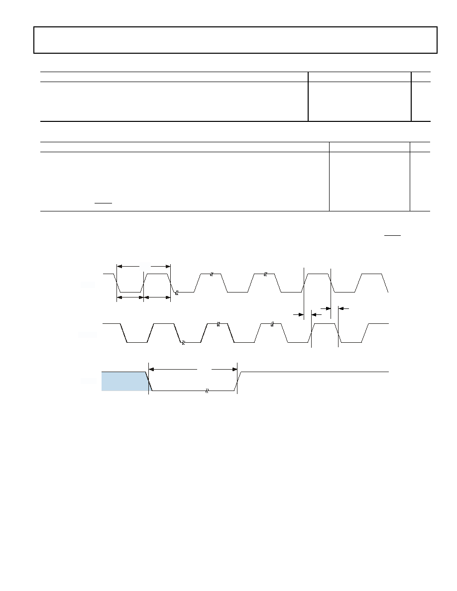
ADSP-BF534/ADSP-BF536/ADSP-BF537
Rev. B
|
Page 27 of 68
|
July 2006
Table 16. System Clock Requirements
Parameter
Condition
Min
Max
Unit
f
SCLK
V
DDEXT
=
3.3 V, V
DDINT
1.14 V
133
MHz
f
SCLK
V
DDEXT
=
3.3 V, V
DDINT
<
1.14 V
100
MHz
f
SCLK
V
DDEXT
=
2.5 V, V
DDINT
1.14 V
133
MHz
f
SCLK
V
DDEXT
=
2.5 V, V
DDINT
<
1.14 V
100
MHz
Table 17. Clock Input and Reset Timing
Parameter
Min
Max
Unit
Timing Requirements
t
CKIN
CLKIN Period
1
25.0
100.0
ns
t
CKINL
CLKIN Low Pulse
2
10.0
ns
t
CKINH
CLKIN High Pulse
2
10.0
ns
t
BUFDLAY
CLKIN to CLKBUF Delay
10
ns
t
WRST
RESET Asserted Pulse Width Low
3
11 t
CKIN
ns
1
Combinations of the CLKIN frequency and the PLL clock multiplier must not exceed the allowed f
VCO
, f
CCLK
, and f
SCLK
settings discussed in
Table 12
through
Table 16
. Since
by default the PLL is multiplying the CLKIN frequency by 10, 300 MHz and 400 MHz speed grade parts can not use the full CLKIN period range.
2
Applies to bypass mode and nonbypass mode.
3
Applies after power-up sequence is complete. At power-up, the processor's internal phase-locked loop requires no more than 2000 CLKIN cycles while RESET is asserted,
assuming stable power supplies and CLKIN (not including start-up time of external clock oscillator).
Figure 9. Clock and Reset Timing
RESET
CLKIN
t
CKINH
t
CKIN
t
CKINL
t
WRST
CLKBUF
t
BUFDLAY
t
BUFDLAY
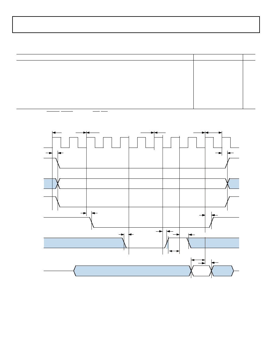
Rev. B
|
Page 28 of 68
|
July 2006
ADSP-BF534/ADSP-BF536/ADSP-BF537
Asynchronous Memory Read Cycle Timing
Table 18. Asynchronous Memory Read Cycle Timing
Parameter
Min
Max
Unit
Timing Requirements
t
SDAT
DATA15 0 Setup Before CLKOUT
2.1
ns
t
HDAT
DATA15 0 Hold After CLKOUT
0.8
ns
t
SARDY
ARDY Setup Before CLKOUT
4.0
ns
t
HARDY
ARDY Hold After CLKOUT
0.0
ns
Switching Characteristics
t
DO
Output Delay After CLKOUT
1
1
Output pins include AMS30, ABE10, ADDR191, AOE, ARE.
6.0
ns
t
HO
Output Hold After CLKOUT
1
0.8
ns
Figure 10. Asynchronous Memory Read Cycle Timing
t
DO
t
SDAT
CLKOUT
AMSx
ABE10
t
HO
BE, ADDRESS
READ
t
HDAT
DATA150
AOE
t
DO
t
SARDY
t
HARDY
ACCESS EXTENDED
3 CYCLES
HOLD
1 CYCLE
ARE
t
HARDY
ARDY
ADDR191
SETUP
2 CYCLES
PROGRAMMED READ ACCESS
4 CYCLES
t
HO
t
SARDY
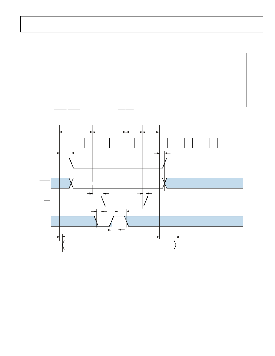
ADSP-BF534/ADSP-BF536/ADSP-BF537
Rev. B
|
Page 29 of 68
|
July 2006
Asynchronous Memory Write Cycle Timing
Table 19. Asynchronous Memory Write Cycle Timing
Parameter
Min
Max
Unit
Timing Requirements
t
SARDY
ARDY Setup Before CLKOUT
4.0
ns
t
HARDY
ARDY Hold After CLKOUT
0.0
ns
Switching Characteristics
t
DDAT
DATA15 0 Disable After CLKOUT
6.0
ns
t
ENDAT
DATA15 0 Enable After CLKOUT
1.0
ns
t
DO
Output Delay After CLKOUT
1
1
Output pins include AMS30, ABE10, ADDR191, DATA150, AOE, AWE.
6.0
ns
t
HO
Output Hold After CLKOUT
1
0.8
ns
Figure 11. Asynchronous Memory Write Cycle Timing
t
DO
t
ENDAT
CLKOUT
AMSx
ABE10
t
HO
WRITE DATA
t
DDAT
DATA150
AWE
t
SARDY
t
HARDY
SETUP
2 CYCLES
PROGRAMMED WRITE
ACCESS 2 CYCLES
ACCESS
EXTENDED
1 CYCLE
HOLD
1 CYCLE
ARDY
ADDR191
t
HO
t
SARDY
t
DO
BE, ADDRESS
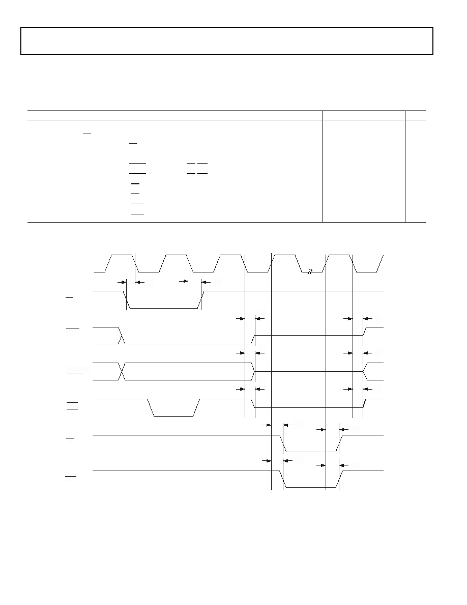
Rev. B
|
Page 30 of 68
|
July 2006
ADSP-BF534/ADSP-BF536/ADSP-BF537
External Port Bus Request and Grant Cycle Timing
Table 20
and
Figure 12
describe external port bus request and
bus grant operations.
Table 20. External Port Bus Request and Grant Cycle Timing
Parameter
1, 2
Min
Max
Unit
Timing Requirements
t
BS
BR Asserted to CLKOUT Low Setup
4.6
ns
t
BH
CLKOUT Low to BR Deasserted Hold Time
0.0
ns
Switching Characteristics
t
SD
CLKOUT Low to AMSx, Address, and RD/WR Disable
4.5
ns
t
SE
CLKOUT Low to AMSx, Address, and RD/WR Enable
4.5
ns
t
DBG
CLKOUT High to BG Asserted Setup
3.6
ns
t
EBG
CLKOUT High to BG Deasserted Hold Time
3.6
ns
t
DBH
CLKOUT High to BGH Asserted Setup
3.6
ns
t
EBH
CLKOUT High to BGH Deasserted Hold Time
3.6
ns
1
These are preliminary timing parameters that are based on worst-case operating conditions.
2
The pad loads for these timing parameters are 20 pF.
Figure 12. External Port Bus Request and Grant Cycle Timing
t
BH
ADDR19-1
AMSx
CLKOUT
t
BS
t
SD
t
SD
t
SD
t
DBG
t
DBH
t
SE
t
SE
t
SE
t
EBG
t
EBH
BG
AWE
BGH
ARE
BR
ABE1-0
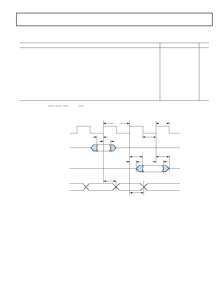
ADSP-BF534/ADSP-BF536/ADSP-BF537
Rev. B
|
Page 31 of 68
|
July 2006
SDRAM Interface Timing
Table 21. SDRAM Interface Timing
Parameter
Min
Max
Unit
Timing Requirements
t
SSDAT
DATA Setup Before CLKOUT
1.5
ns
t
HSDAT
DATA Hold After CLKOUT
0.8
ns
Switching Characteristics
t
SCLK
CLKOUT Period
1
1
The t
SCLK
value is the inverse of the f
SCLK
specification discussed in
Table 16
. Package type and reduced supply voltages affect the best-case value of 7.5 ns listed here.
7.5
ns
t
SCLKH
CLKOUT Width High
2.5
ns
t
SCLKL
CLKOUT Width Low
2.5
ns
t
DCAD
Command, ADDR, Data Delay After CLKOUT
2
2
Command pins include: SRAS, SCAS, SWE, SDQM, SMS, SA10, SCKE.
4.0
ns
t
HCAD
Command, ADDR, Data Hold After CLKOUT
2
1.0
ns
t
DSDAT
Data Disable After CLKOUT
6.0
ns
t
ENSDAT
Data Enable After CLKOUT
1.0
ns
Figure 13. SDRAM Interface Timing
t
HCAD
t
HCAD
t
DSDAT
t
DCAD
t
SSDAT
t
DCAD
t
ENSDAT
t
HSDAT
t
SCLKL
t
SCLKH
t
SCLK
CLKOUT
DATA (IN)
DATA (OUT)
COMMAND ADDR
(OUT)
NOTE: COMMAND =
SRAS
,
SCAS
,
SWE
, SDQM,
SMS
, SA10, SCKE.
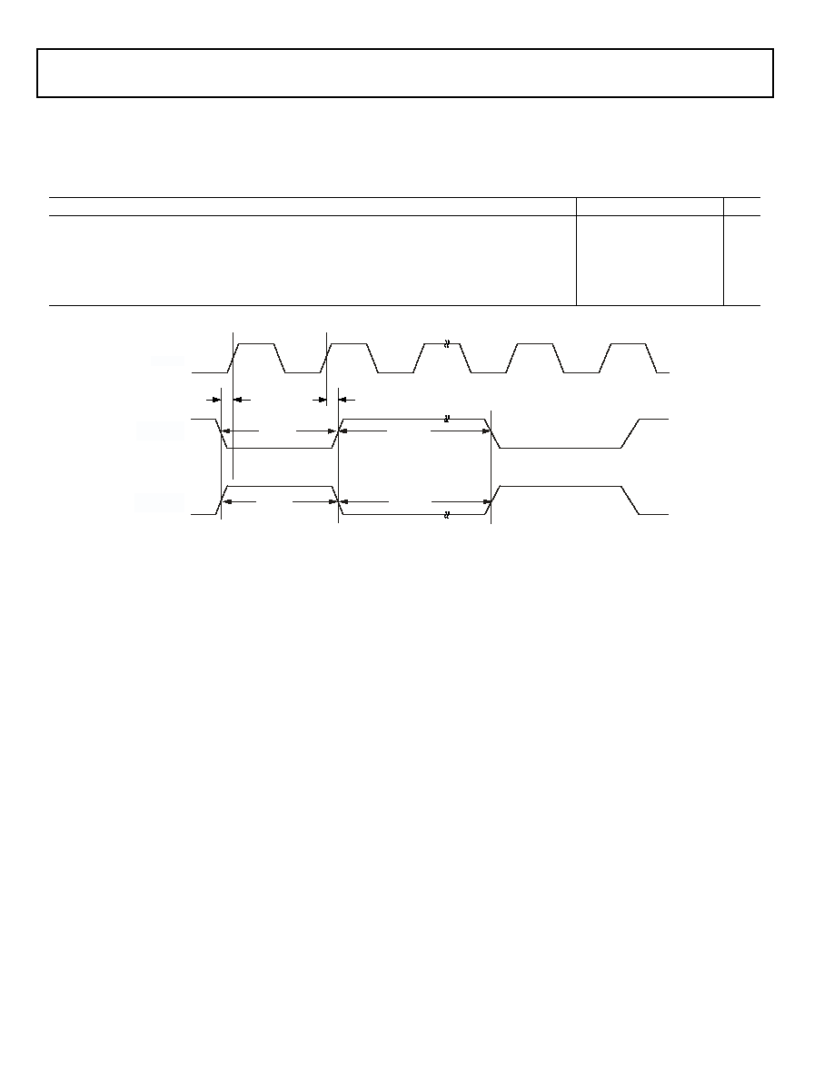
Rev. B
|
Page 32 of 68
|
July 2006
ADSP-BF534/ADSP-BF536/ADSP-BF537
External DMA Request Timing
Table 22
and
Figure 14
describe the external DMA request
operations.
Table 22. External DMA Request Timing
Parameter
Min
Max
Unit
Timing Requirements
t
DR
DMARx Asserted to CLKOUT High Setup
6.0
ns
t
DH
CLKOUT High to DMARx Deasserted Hold Time
0.0
ns
t
DMARACT
DMARx Active Pulse Width
1.0
×
t
SCLK
ns
t
DMARINACT
DMARx Inactive Pulse Width
1.75
×
t
SCLK
ns
Figure 14. External DMA Request Timing
CLKOUT
t
DR
DMAR0/1
(Active Low)
t
DH
DMAR0/1
(Active High)
t
DMARACT
t
DMARINACT
t
DMARINACT
t
DMARACT
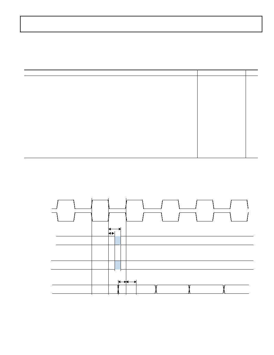
ADSP-BF534/ADSP-BF536/ADSP-BF537
Rev. B
|
Page 33 of 68
|
July 2006
Parallel Peripheral Interface Timing
Table 23
and
Figure 15 on Page 33
,
Figure 19 on Page 37
, and
Figure 20 on Page 38
describe parallel peripheral interface
operations.
Table 23. Parallel Peripheral Interface Timing
Parameter
Min
Max
Unit
Timing Requirements
t
PCLKW
PPI_CLK Width
1
6.0
ns
t
PCLK
PPI_CLK Period
1
15.0
ns
Timing Requirements--GP Input and Frame Capture Modes
t
SFSPE
External Frame Sync Setup Before PPI_CLK
(Nonsampling Edge for Rx, Sampling Edge for Tx)
6.7
ns
t
HFSPE
External Frame Sync Hold After PPI_CLK
1.0
ns
t
SDRPE
Receive Data Setup Before PPI_CLK
3.5
ns
t
HDRPE
Receive Data Hold After PPI_CLK
1.5
ns
Switching Characteristics--GP Output and Frame Capture Modes
t
DFSPE
Internal Frame Sync Delay After PPI_CLK
8.0
ns
t
HOFSPE
Internal Frame Sync Hold After PPI_CLK
1.7
ns
t
DDTPE
Transmit Data Delay After PPI_CLK
8.0
ns
t
HDTPE
Transmit Data Hold After PPI_CLK
1.8
ns
1
PPI_CLK frequency cannot exceed f
SCLK
/2.
Figure 15. PPI GP Rx Mode with Internal Frame Sync Timing
t
S
DRPE
t
HDRPE
POL
S
= 0
POL
S
= 0
POLC = 0
POL
S
= 1
POL
S
= 1
FRAME
S
YNC
DRIVING
EDGE
DATA
S
AMPLING
EDGE
DATA
S
AMPLING
EDGE
POLC = 1
t
DF
S
PE
t
HOF
S
PE
PPI_CLK
PPI_CLK
PPI_F
S
1
PPI_F
S
2
PPI_DATA
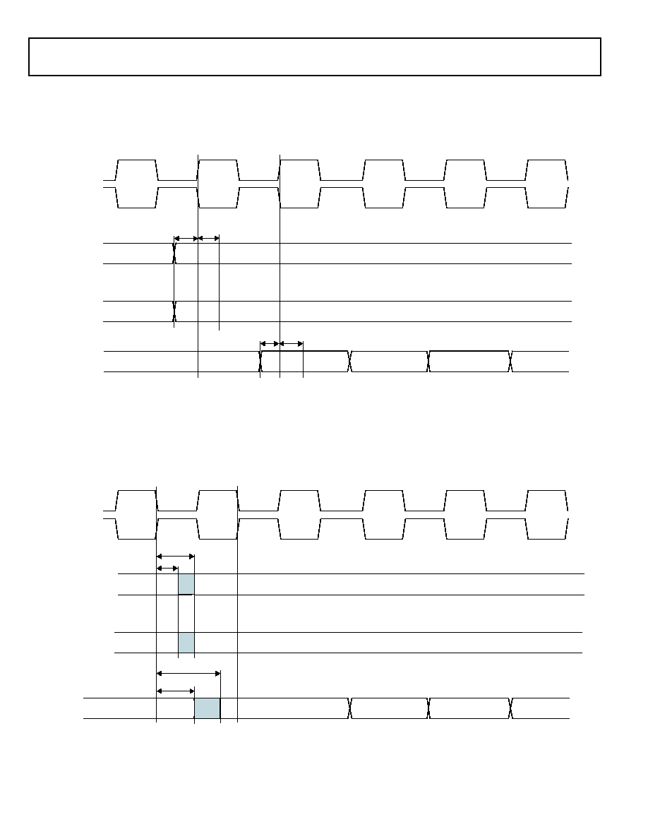
Rev. B
|
Page 34 of 68
|
July 2006
ADSP-BF534/ADSP-BF536/ADSP-BF537
Figure 16. PPI GP Rx Mode with External Frame Sync Timing
Figure 17. PPI GP Tx Mode with Internal Frame Sync Timing
POL
S
= 0
POL
S
= 0
POLC = 0
POL
S
= 1
POL
S
= 1
DATA
S
AMPLING/
FRAME
S
YNC
S
AMPLING
EDGE
DATA
S
AMPLING/
FRAME
S
YNC
S
AMPLING
EDGE
POLC = 1
t
HF
S
PE
t
S
F
S
PE
PPI_DATA
PPI_CLK
PPI_CLK
PPI_F
S
1
PPI_F
S
2
t
S
DRPE
t
HDRPE
t
HDTPE
t
DDTPE
POL
S
= 0
POL
S
= 0
POLC = 0
POL
S
= 1
POL
S
= 1
DATA
DRIVING/
FRAME
S
YNC
DRIVING
EDGE
DATA
DRIVING/
FRAME
S
YNC
DRIVING
EDGE
POLC = 1
t
DF
S
PE
t
HOF
S
PE
PPI_DATA
PPI_CLK
PPI_CLK
PPI_F
S
1
PPI_F
S
2
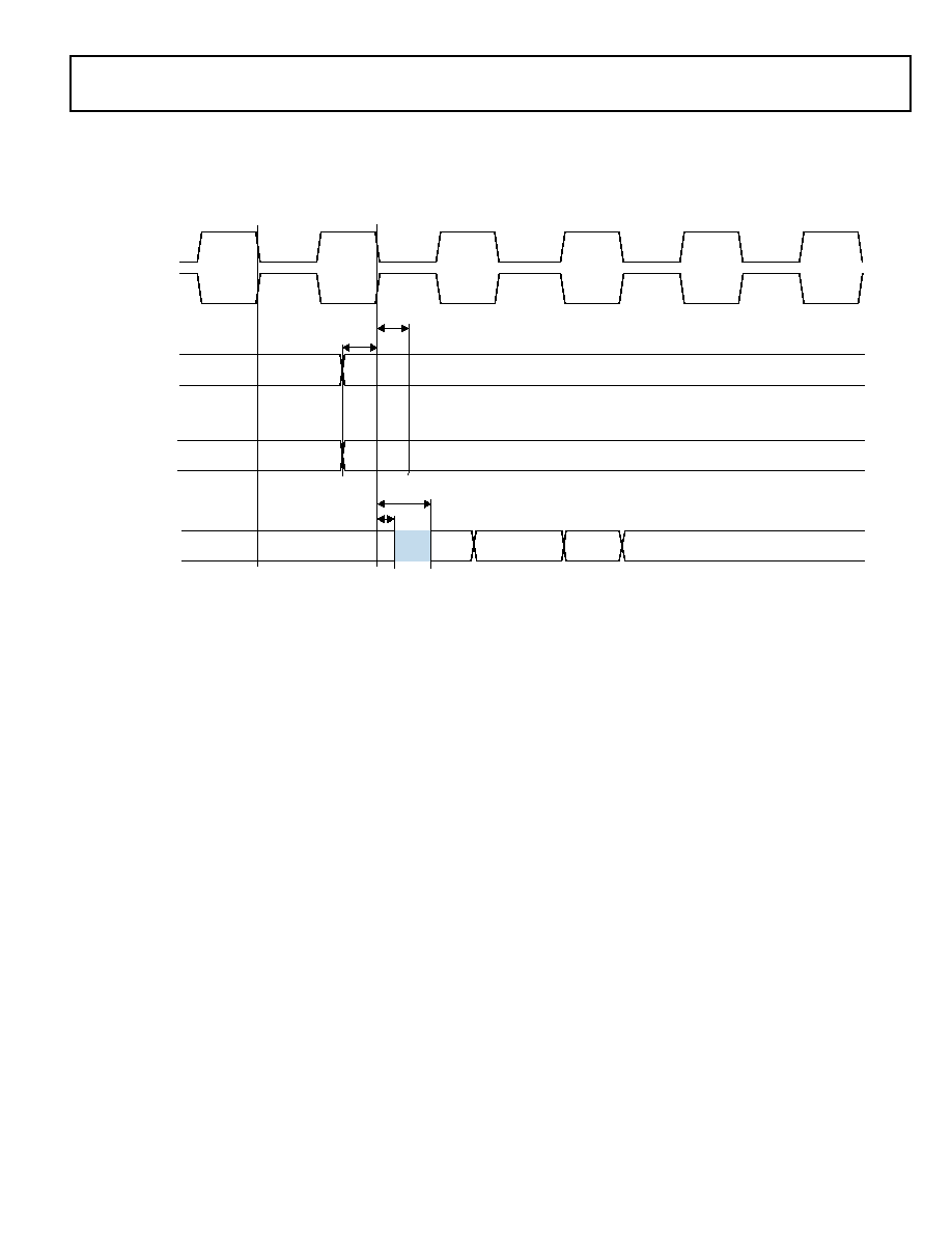
ADSP-BF534/ADSP-BF536/ADSP-BF537
Rev. B
|
Page 35 of 68
|
July 2006
Figure 18. PPI GP Tx Mode with External Frame Sync Timing
t
HDTPE
t
DDTPE
POL
S
= 0
POL
S
= 0
POLC = 0
POL
S
= 1
POL
S
= 1
DATA
DRIVING/
FRAME
S
YNC
S
AMPLING
EDGE
DATA
DRIVING/
FRAME
S
YNC
S
AMPLING
EDGE
POLC = 1
t
HF
S
PE
t
S
F
S
PE
PPI_DATA
PPI_CLK
PPI_CLK
PPI_F
S
1
PPI_F
S
2

Rev. B
|
Page 36 of 68
|
July 2006
ADSP-BF534/ADSP-BF536/ADSP-BF537
Serial Ports
Table 24
through
Table 27 on Page 37
and
Figure 19 on Page 37
through
Figure 21 on Page 39
describe serial port operations.
Table 24. Serial Ports--External Clock
Parameter
Min
Max
Unit
Timing Requirements
t
SFSE
TFS/RFS Setup Before TSCLK/RSCLK
1
3.0
ns
t
HFSE
TFS/RFS Hold After TSCLK/RSCLK
1
3.0
ns
t
SDRE
Receive Data Setup Before RSCLK
1
3.0
ns
t
HDRE
Receive Data Hold After RSCLK
1
3.0
ns
t
SCLKEW
TSCLK/RSCLK Width
4.5
ns
t
SCLKE
TSCLK/RSCLK Period
15.0
ns
Switching Characteristics
t
DFSE
TFS/RFS Delay After TSCLK/RSCLK (Internally Generated TFS/RFS)
2
10.0
ns
t
HOFSE
TFS/RFS Hold After TSCLK/RSCLK (Internally Generated TFS/RFS)
2
0
ns
t
DDTE
Transmit Data Delay After TSCLK
2
10.0
ns
t
HDTE
Transmit Data Hold After TSCLK
2
0
ns
1
Referenced to sample edge.
2
Referenced to drive edge.
Table 25. Serial Ports--Internal Clock
Parameter
Min
Max
Unit
Timing Requirements
t
SFSI
TFS/RFS Setup Before TSCLK/RSCLK
1
8.0
ns
t
HFSI
TFS/RFS Hold After TSCLK/RSCLK
1
1.5
ns
t
SDRI
Receive Data Setup Before RSCLK
1
8.0
ns
t
HDRI
Receive Data Hold After RSCLK
1
1.5
ns
t
SCLKEW
TSCLK/RSCLK Width
4.5
ns
t
SCLKE
TSCLK/RSCLK Period
15.0
ns
Switching Characteristics
t
DFSI
TFS/RFS Delay After TSCLK/RSCLK (Internally Generated TFS/RFS)
2
3.0
ns
t
HOFSI
TFS/RFS Hold After TSCLK/RSCLK (Internally Generated TFS/RFS)
2
-
1.0
ns
t
DDTI
Transmit Data Delay After TSCLK
2
3.0
ns
t
HDTI
Transmit Data Hold After TSCLK
2
-
1.0
ns
t
SCLKIW
TSCLK/RSCLK Width
4.5
ns
1
Referenced to sample edge.
2
Referenced to drive edge.
Table 26. Serial Ports--Enable and Three-State
Parameter
Min
Max
Unit
Switching Characteristics
t
DTENE
Data Enable Delay from External TSCLK
1
0
ns
t
DDTTE
Data Disable Delay from External TSCLK
1
10.0
ns
t
DTENI
Data Enable Delay from Internal TSCLK
1
2.0
ns
t
DDTTI
Data Disable Delay from Internal TSCLK
1
3.0
ns
1
Referenced to drive edge.
ADSP-BF534/ADSP-BF536/ADSP-BF537
Rev. B
|
Page 37 of 68
|
July 2006
Table 27. External Late Frame Sync
Parameter
Min
Max
Unit
Switching Characteristics
t
DDTLFSE
Data Delay from Late External TFS or External RFS with MCE = 1, MFD = 0
1, 2
10.0
ns
t
DTENLFS
Data Enable from Late FS or MCE = 1, MFD = 0
1, 2
0
ns
1
MCE = 1, TFS enable and TFS valid follow t
DDTENFS
and t
DDTLFS
.
2
If external RFS/TFS setup to RSCLK/TSCLK > t
SCLKE
/2, then t
DDTE/I
and t
DTENE/I
apply, otherwise t
DDTLFSE
and t
DTENLFS
apply.
Figure 19. Serial Ports
DT
DT
t
DDTTE
t
DDTENE
t
DDTTI
t
DDTENI
DRIVE
EDGE
DRIVE
EDGE
DRIVE
EDGE
DRIVE
EDGE
TSCLK/RSCLK
TSCLK/RSCLK
TSCLK (EXT.)
TFS ("LATE," EXT.)
TSCLK (INT.)
TFS ("LATE," INT.)
t
SDRI
RSCLK
RFS
DR
DRIVE
EDGE
SAMPLE
EDGE
t
HDRI
t
SFSI
t
HFSI
t
DFSE
t
HOFSE
t
SCLKIW
DATA RECEIVE-INTERNAL CLOCK
t
SDRE
DATA RECEIVE-EXTERNAL CLOCK
RSCLK
RFS
DR
DRIVE
EDGE
SAMPLE
EDGE
t
HDRE
t
SFSE
t
HFSE
t
DFSE
t
SCLKEW
t
HOFSE
NOTE: EITHER THE RISING EDGE OR FALLING EDGE OF RCLK, TCLK CAN BE USED AS THE ACTIVE SAMPLING EDGE.
t
DDTI
t
HDTI
TSCLK
TFS
DT
DRIVE
EDGE
SAMPLE
EDGE
t
SFSI
t
HFSI
t
SCLKIW
t
DFSI
t
HOFSI
DATA TRANSMIT-INTERNAL CLOCK
t
DDTE
t
HDTE
TSCLK
TFS
DT
DRIVE
EDGE
SAMPLE
EDGE
t
SFSE
t
HFSE
t
DFSE
t
SCLKEW
t
HOFSE
DATA TRANSMIT-EXTERNAL CLOCK
NOTE: EITHER THE RISING EDGE OR FALLING EDGE OF RCLK OR TCLK CAN BE USED AS THE ACTIVE SAMPLING EDGE.
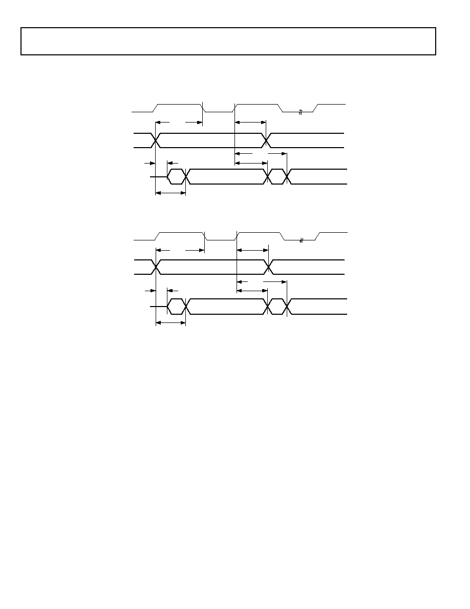
Rev. B
|
Page 38 of 68
|
July 2006
ADSP-BF534/ADSP-BF536/ADSP-BF537
Figure 20. External Late Frame Sync (Frame Sync Setup < t
SCLKE
/2)
t
DDTLFSE
t
SFSE/I
t
HDTE/I
RSCLK
DRIVE
DRIVE
SAMPLE
RFS
DT
2ND BIT
1ST BIT
t
DTENLFS
t
DDTE/I
t
HOFSE/I
t
DTENLFS
t
SFSE/I
t
HDTE/I
DRIVE
DRIVE
SAMPLE
DT
TSCLK
TFS
2ND BIT
1ST BIT
t
DDTLFSE
t
DDTE/I
t
HOFSE/I
EXTERNAL RFS WITH MCE = 1, MFD = 0
LATE EXTERNAL TFS
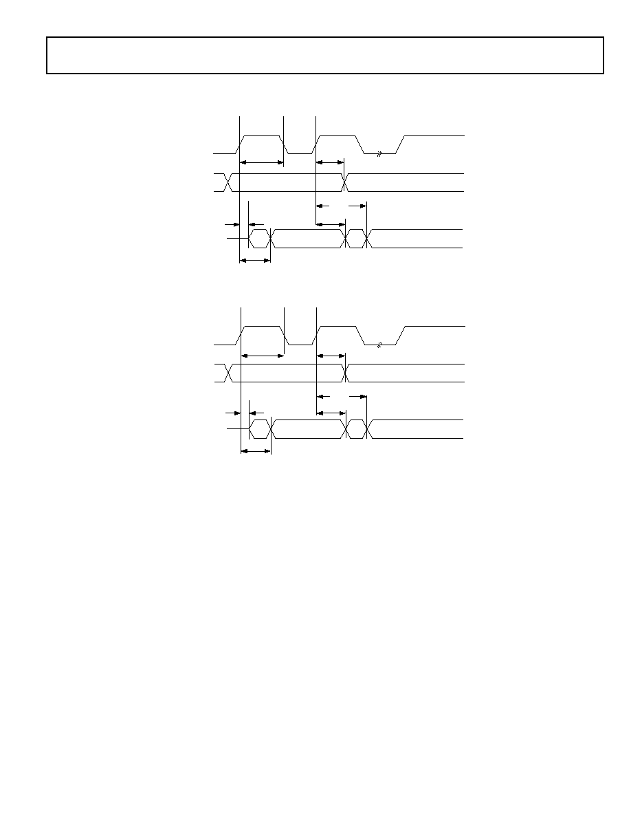
ADSP-BF534/ADSP-BF536/ADSP-BF537
Rev. B
|
Page 39 of 68
|
July 2006
Figure 21. External Late Frame Sync (Frame Sync Setup > t
SCLKE
/2)
DT
RSCLK
RFS
t
SFSE/I
t
HOFSE/I
t
DTENLSCK
t
DDTE/I
t
HDTE/I
t
DDTLSCK
DRIVE
SAMPLE
1ST BIT
2ND BIT
DRIVE
DT
TSCLK
TFS
t
SFSE/I
t
HOFSE/I
t
DTENLSCK
t
DDTE/I
t
HDTE/I
t
DDTLSCK
DRIVE
SAMPLE
1ST BIT
2ND BIT
DRIVE
LATE EXTERNAL TFS
EXTERNAL RFS WITH MCE = 1, MFD = 0
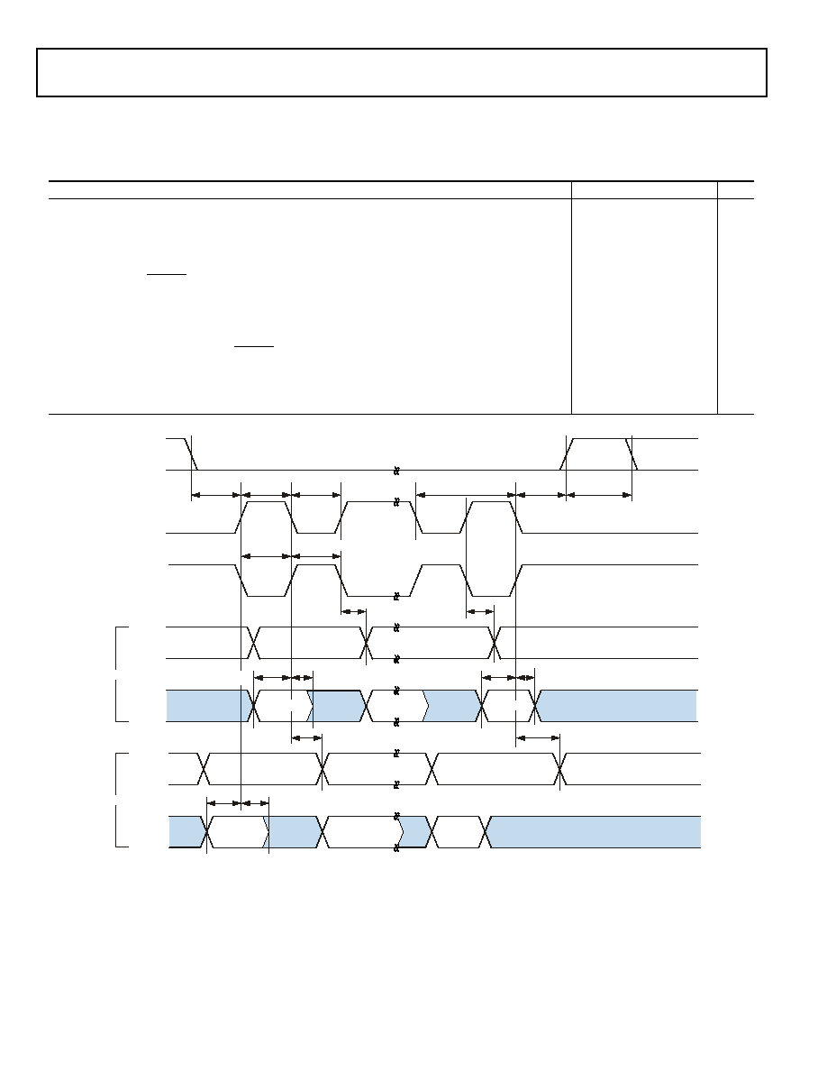
Rev. B
|
Page 40 of 68
|
July 2006
ADSP-BF534/ADSP-BF536/ADSP-BF537
Serial Peripheral Interface Port--Master Timing
Table 28
and
Figure 22
describe SPI port master operations.
Table 28. Serial Peripheral Interface (SPI) Port--Master Timing
Parameter
Min
Max
Unit
Timing Requirements
t
SSPIDM
Data Input Valid to SCK Edge (Data Input Setup)
7.5
ns
t
HSPIDM
SCK Sampling Edge to Data Input Invalid
1.5
ns
Switching Characteristics
t
SDSCIM
SPISELx Low to First SCK Edge (x = 0 or x = 1)
2
×
t
SCLK
1.5
ns
t
SPICHM
Serial Clock High Period
2
×
t
SCLK
1.5
ns
t
SPICLM
Serial Clock Low Period
2
×
t
SCLK
1.5
ns
t
SPICLK
Serial Clock Period
4
×
t
SCLK
1.5
ns
t
HDSM
Last SCK Edge to SPISELx High (x = 0 or x = 1)
2
×
t
SCLK
1.5
ns
t
SPITDM
Sequential Transfer Delay
2
×
t
SCLK
1.5
ns
t
DDSPIDM
SCK Edge to Data Out Valid (Data Out Delay)
0
6
ns
t
HDSPIDM
SCK Edge to Data Out Invalid (Data Out Hold)
1.0
+4.0
ns
Figure 22. Serial Peripheral Interface (SPI) Port--Master Timing
t
SSPIDM
t
HSPIDM
t
HDSPIDM
LSB
MSB
t
HSPIDM
t
DDSPIDM
MOSI
(OUTPUT)
MISO
(INPUT)
SPISELx
(OUTPUT)
SCK
(CPOL = 0)
(OUTPUT)
SCK
(CPOL = 1)
(OUTPUT)
t
SPICHM
t
SPICLM
t
SPICLM
t
SPICLK
t
SPICHM
t
HDSM
t
SPITDM
t
HDSPIDM
LSB VALID
LSB
MSB
MSB VALID
t
HSPIDM
t
DDSPIDM
MOSI
(OUTPUT)
MISO
(INPUT)
t
SSPIDM
CPHA = 1
CPHA = 0
MSB VALID
t
SDSCIM
t
SSPIDM
LSB VALID
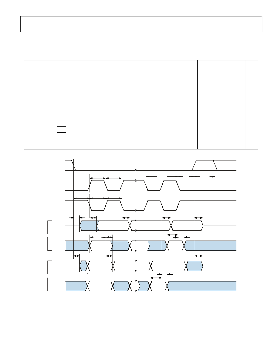
ADSP-BF534/ADSP-BF536/ADSP-BF537
Rev. B
|
Page 41 of 68
|
July 2006
Serial Peripheral Interface Port--Slave Timing
Table 29
and
Figure 23
describe SPI port slave operations.
Table 29. Serial Peripheral Interface (SPI) Port--Slave Timing
Parameter
Min
Max
Unit
Timing Requirements
t
SPICHS
Serial Clock High Period
2
×
t
SCLK
1.5
ns
t
SPICLS
Serial Clock Low Period
2
×
t
SCLK
1.5
ns
t
SPICLK
Serial Clock Period
4
×
t
SCLK
1.5
ns
t
HDS
Last SCK Edge to SPISS Not Asserted
2
×
t
SCLK
1.5
ns
t
SPITDS
Sequential Transfer Delay
2
×
t
SCLK
1.5
ns
t
SDSCI
SPISS Assertion to First SCK Edge
2
×
t
SCLK
1.5
ns
t
SSPID
Data Input Valid to SCK Edge (Data Input Setup)
1.6
ns
t
HSPID
SCK Sampling Edge to Data Input Invalid
1.6
ns
Switching Characteristics
t
DSOE
SPISS Assertion to Data Out Active
0
8
ns
t
DSDHI
SPISS Deassertion to Data High Impedance
0
8
ns
t
DDSPID
SCK Edge to Data Out Valid (Data Out Delay)
0
10
ns
t
HDSPID
SCK Edge to Data Out Invalid (Data Out Hold)
0
10
ns
Figure 23. Serial Peripheral Interface (SPI) Port--Slave Timing
t
HSPID
t
DDSPID
t
DSDHI
LSB
MSB
MSB VALID
t
HSPID
t
DSOE
t
DDSPID
t
HDSPID
MISO
(OUTPUT)
MOSI
(INPUT)
t
SSPID
SPISS
(INPUT)
SCK
(CPOL = 0)
(INPUT)
SCK
(CPOL = 1)
(INPUT)
t
SDSCI
t
SPICHS
t
SPICLS
t
SPICLS
t
SPICLK
t
HDS
t
SPICHS
t
SSPID
t
HSPID
t
DSDHI
LSB VALID
MSB
MSB VALID
t
DSOE
t
DDSPID
MISO
(OUTPUT)
MOSI
(INPUT)
t
SSPID
LSB VALID
LSB
CPHA = 1
CPHA = 0
t
SPITDS
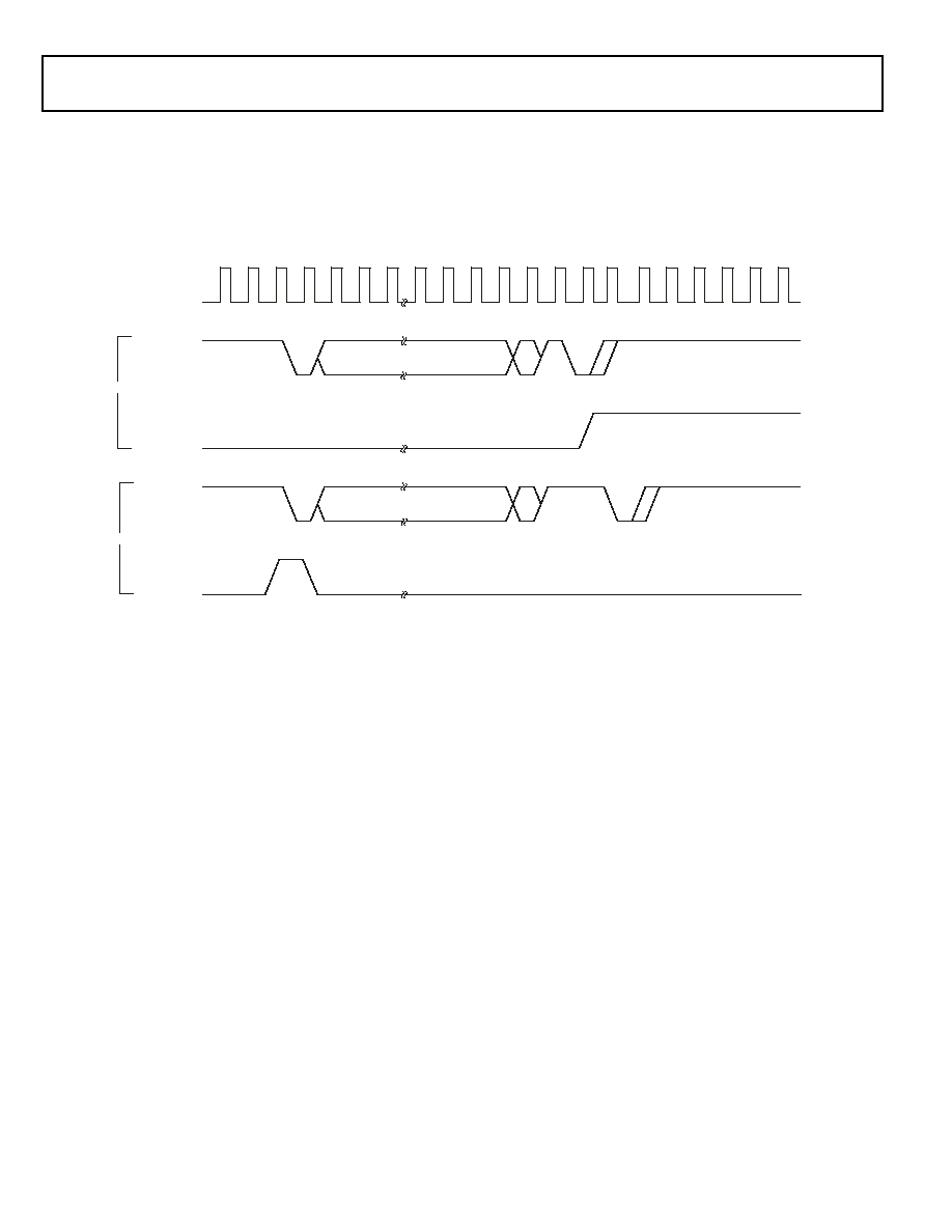
Rev. B
|
Page 42 of 68
|
July 2006
ADSP-BF534/ADSP-BF536/ADSP-BF537
Universal Asynchronous Receiver-Transmitter
(UART) Ports--Receive and Transmit Timing
Figure 24
describes the UART ports receive and transmit opera-
tions. The maximum baud rate is SCLK/16. As shown in
Figure 24
there is some latency between the generation of
internal UART interrupts and the external data operations.
These latencies are negligible at the data transmission rates for
the UART.
Figure 24. UART Ports--Receive and Transmit Timing
UARTX Rx
DATA(58)
INTERNAL
UART RECEIVE
INTERRUPT
UART RECEIVE BIT SET BY DATA STOP;
CLEARED BY FIFO READ
CLKOUT
(SAMPLE CLOCK)
UARTX Tx
DATA(58)
STOP (12)
INTERNAL
UART TRANSMIT
INTERRUPT
UART TRANSMIT BIT SET BY PROGRAM;
CLEARED BY WRITE TO TRANSMIT
START
STOP
TRANSMIT
RECEIVE
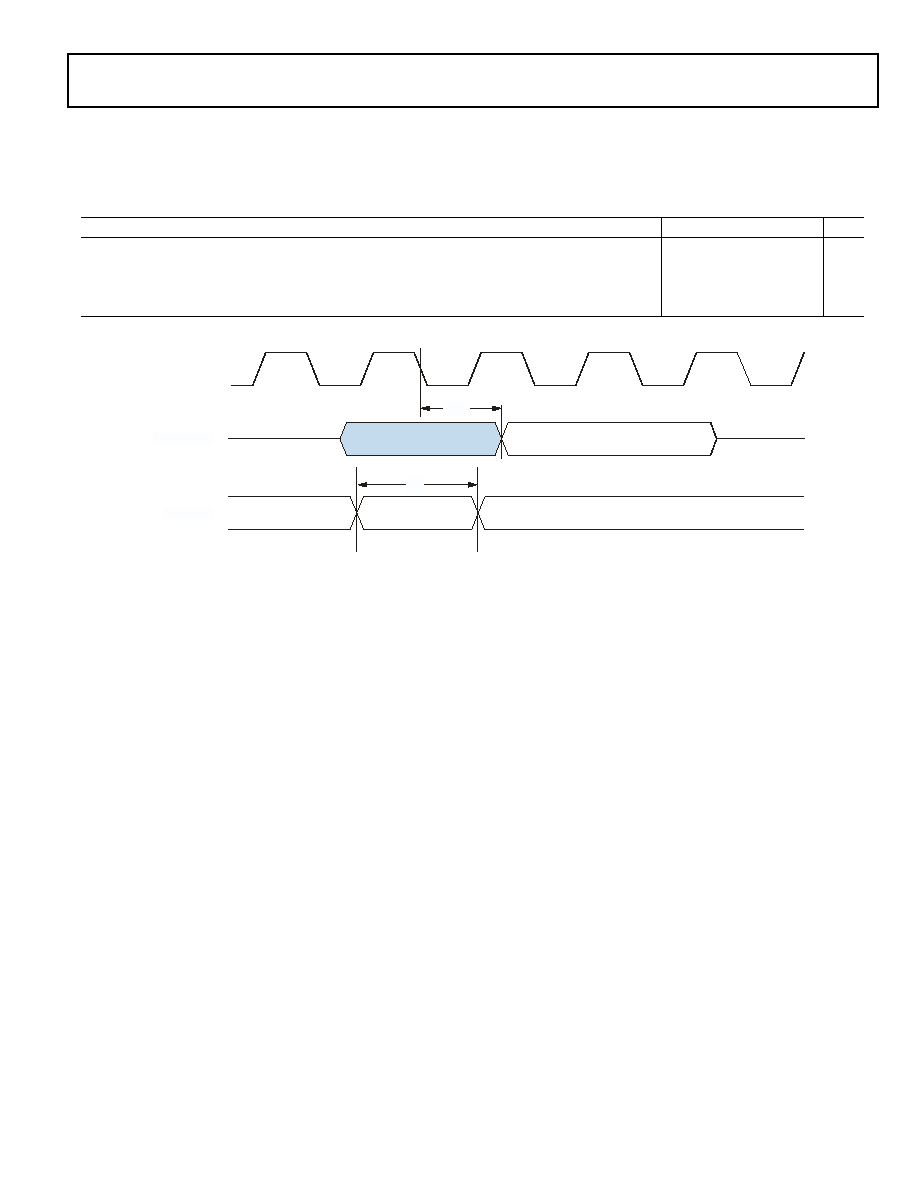
ADSP-BF534/ADSP-BF536/ADSP-BF537
Rev. B
|
Page 43 of 68
|
July 2006
General-Purpose Port Timing
Table 30
and
Figure 25
describe general-purpose
port operations.
Table 30. General-Purpose Port Timing
Parameter
Min
Max
Unit
Timing Requirement
t
WFI
General-Purpose Port Pin Input Pulse Width
t
SCLK
+ 1
ns
Switching Characteristic
t
GPOD
General-Purpose Port Pin Output Delay from CLKOUT Low
0
6
ns
Figure 25. General-Purpose Port Timing
GPP INPUT
GPP OUTPUT
CLKOUT
t
GPOD
t
WFI
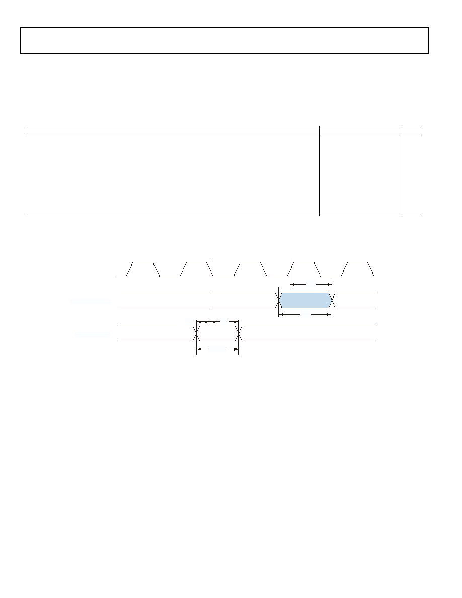
Rev. B
|
Page 44 of 68
|
July 2006
ADSP-BF534/ADSP-BF536/ADSP-BF537
Timer Cycle Timing
Table 31
and
Figure 26
describe timer expired operations. The
input signal is asynchronous in "width capture mode" and
"external clock mode" and has an absolute maximum input fre-
quency of (f
SCLK
/2) MHz.
Table 31. Timer Cycle Timing
Parameter
Min
Max
Unit
Timing Characteristics
t
WL
Timer Pulse Width Input Low (Measured In SCLK Cycles)
1
1
×
t
SCLK
ns
t
WH
Timer Pulse Width Input High (Measured In SCLK Cycles)
1
1
×
t
SCLK
ns
t
TIS
Timer Input Setup Time Before CLKOUT Low
2
5
ns
t
TIH
Timer Input Hold Time After CLKOUT Low
2
2
ns
Switching Characteristics
t
HTO
Timer Pulse Width Output (Measured In SCLK Cycles)
1
×
t
SCLK
(2
32
1)
×
t
SCLK
ns
t
TOD
Timer Output Update Delay After CLKOUT High
6
ns
1
The minimum pulse widths apply for TMRx signals in width capture and external clock modes. They also apply to the PF15 or PPI_CLK signals in PWM output mode.
2
Either a valid setup and hold time or a valid pulse width is sufficient. There is no need to resynchronize programmable flag inputs.
Figure 26. Timer Cycle Timing
TIM E R IN PU T
TIME R O U TPU T
C LK O U T
t
T IS
t
TIH
t
TO D
t
W H ,
t
W L
t
H T O
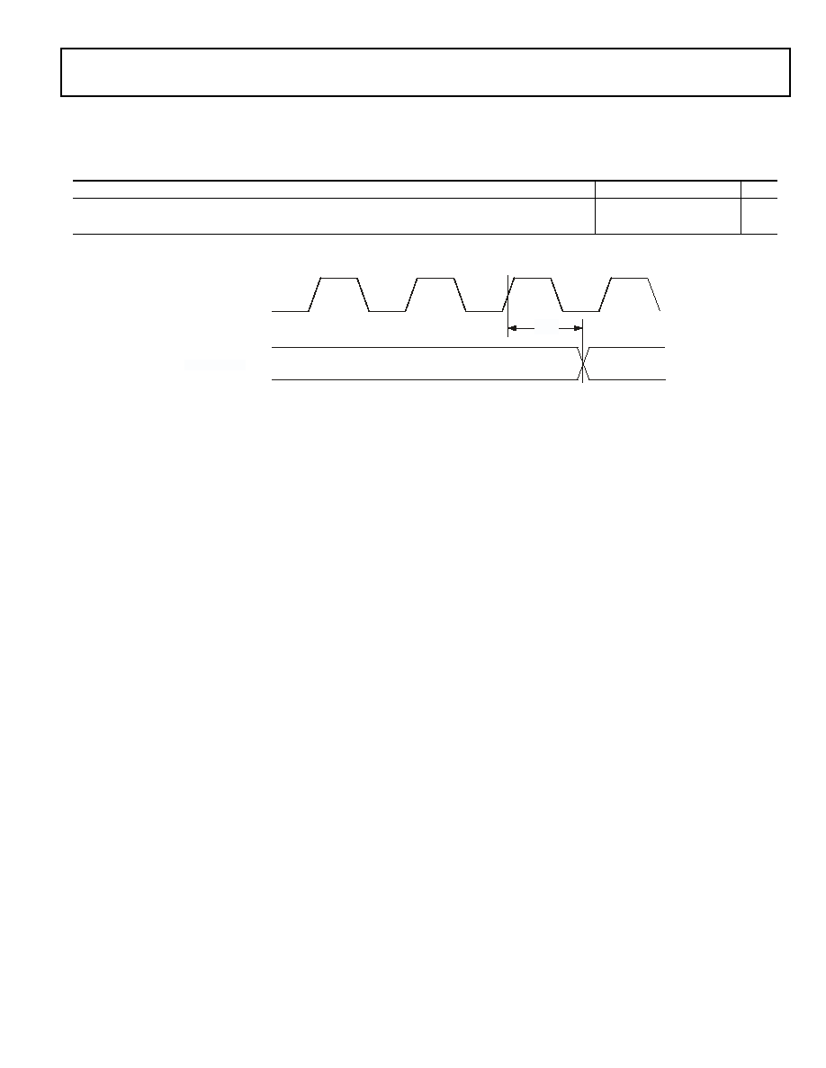
ADSP-BF534/ADSP-BF536/ADSP-BF537
Rev. B
|
Page 45 of 68
|
July 2006
Timer Clock Timing
Table 32
and
Figure 27
describe timer clock timing.
Table 32. Timer Clock Timing
Parameter
Min
Max
Unit
Switching Characteristic
t
TODP
Timer Output Update Delay After PPICLK High
12
ns
Figure 27. Timer Clock Timing
TIMER OUTPUT
PPI CLOCK
t
TODP
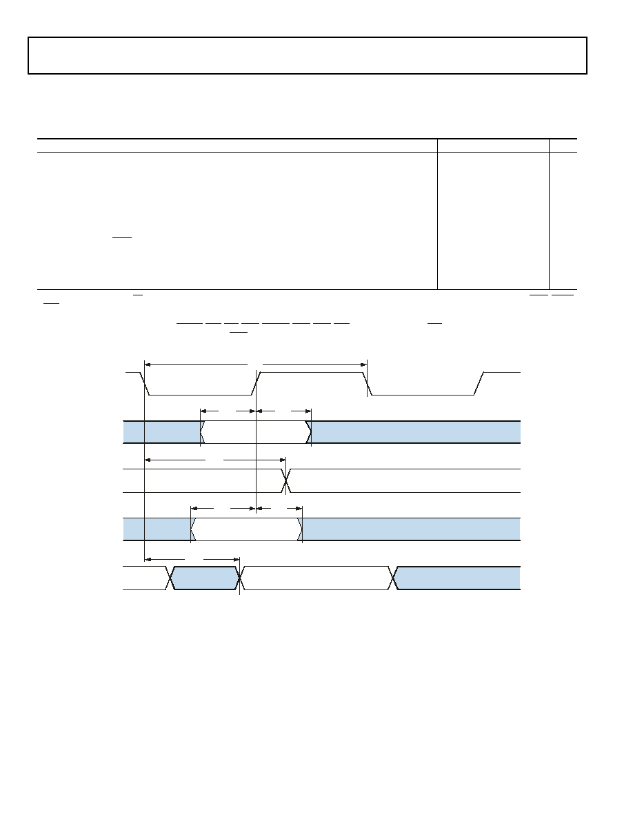
Rev. B
|
Page 46 of 68
|
July 2006
ADSP-BF534/ADSP-BF536/ADSP-BF537
JTAG Test and Emulation Port Timing
Table 33
and
Figure 28
describe JTAG port operations.
Table 33. JTAG Port Timing
Parameter
Min
Max
Unit
Timing Parameters
t
TCK
TCK Period
20
ns
t
STAP
TDI, TMS Setup Before TCK High
4
ns
t
HTAP
TDI, TMS Hold After TCK High
4
ns
t
SSYS
System Inputs Setup Before TCK High
1
4
ns
t
HSYS
System Inputs Hold After TCK High
1
5
ns
t
TRSTW
TRST Pulse Width
2
(Measured in TCK Cycles)
4
TCK
Switching Characteristics
t
DTDO
TDO Delay From TCK Low
10
ns
t
DSYS
System Outputs Delay After TCK Low
3
0
12
ns
1
System Inputs = DATA150, BR, ARDY, SCL, SDA, TFS0, TSCLK0, RSCLK0, RFS0, DR0PRI, DR0SEC, PF150, PG150, PH150, MDIO, TCK, TD1, TMS, TRST, RESET,
NMI, BMODE20.
2
50 MHz maximum
3
System Outputs = DATA150, ADDR191, ABE10, AOE, ARE, AWE, AMS30, SRAS, SCAS, SWE, SCKE, CLKOUT, SA10, SMS, SCL, SDA, TSCLK0, TFS0, RFS0, RSCLK0,
DT0PRI, DT0SEC, PF150, PG150, PH150, RTX0, TD0, EMU, XTAL, VROUT.
Figure 28. JTAG Port Timing
TMS
TDI
TDO
SYSTEM
INPUTS
SYSTEM
OUTPUTS
TCK
t
TCK
t
HTAP
t
STAP
t
DTDO
t
SSYS
t
HSYS
t
DSYS

ADSP-BF534/ADSP-BF536/ADSP-BF537
Rev. B
|
Page 47 of 68
|
July 2006
10/100 Ethernet MAC Controller Timing
Table 34
through
Table 39
and
Figure 29
through
Figure 34
describe the 10/100 Ethernet MAC controller operations. This
feature is only available on the ADSP-BF536 and ADSP-BF537
processors. For more information, see
Table 1 on Page 3
.
Table 34. 10/100 Ethernet MAC Controller Timing: MII Receive Signal
Parameter
1
Min
Max
Unit
t
ERXCLKF
ERxCLK Frequency (f
SCLK
= SCLK Frequency)
None
25 MHz + 1%
f
SCLK
+ 1%
ns
t
ERXCLKW
ERxCLK Width (t
ERxCLK
= ERxCLK Period)
t
ERxCLK
×
35%
t
ERxCLK
×
65%
ns
t
ERXCLKIS
Rx Input Valid to ERxCLK Rising Edge (Data In Setup)
7.5
ns
t
ERXCLKIH
ERxCLK Rising Edge to Rx Input Invalid (Data In Hold)
7.5
ns
1
MII inputs synchronous to ERxCLK are ERxD30, ERxDV, and ERxER.
Table 35. 10/100 Ethernet MAC Controller Timing: MII Transmit Signal
Parameter
1
Min
Max
Unit
t
ETF
ETxCLK Frequency (f
SCLK
= SCLK Frequency)
None
25 MHz + 1%
f
SCLK
+ 1%
ns
t
ETXCLKW
ETxCLK Width (t
ETxCLK
= ETxCLK Period)
t
ETxCLK
×
35%
t
ETxCLK
×
65%
ns
t
ETXCLKOV
ETxCLK Rising Edge to Tx Output Valid (Data Out Valid)
20
ns
t
ETXCLKOH
ETxCLK Rising Edge to Tx Output Invalid (Data Out Hold)
0
ns
1
MII outputs synchronous to ETxCLK are ETxD30.
Table 36. 10/100 Ethernet MAC Controller Timing: RMII Receive Signal
Parameter
1
Min
Max
Unit
t
EREFCLKF
REF_CLK Frequency (f
SCLK
= SCLK Frequency)
None
50 MHz + 1%
2
×
f
SCLK
+ 1%
ns
t
EREFCLKW
EREF_CLK Width (t
EREFCLK
= EREFCLK Period)
t
EREFCLK
×
35%
t
EREFCLK
×
65%
ns
t
EREFCLKIS
Rx Input Valid to RMII REF_CLK Rising Edge (Data In Setup)
4
ns
t
EREFCLKIH
RMII REF_CLK Rising Edge to Rx Input Invalid (Data In Hold)
2
ns
1
RMII inputs synchronous to RMII REF_CLK are ERxD10, RMII CRS_DV, and ERxER.
Table 37. 10/100 Ethernet MAC Controller Timing: RMII Transmit Signal
Parameter
1
Min
Max
Unit
t
EREFCLKOV
RMII REF_CLK Rising Edge to Tx Output Valid (Data Out Valid)
7.5
ns
t
EREFCLKOH
RMII REF_CLK Rising Edge to Tx Output Invalid (Data Out Hold)
2
ns
1
RMII outputs synchronous to RMII REF_CLK are ETxD10.
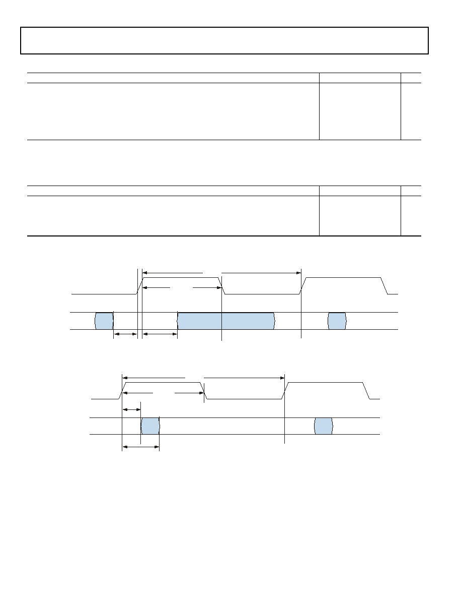
Rev. B
|
Page 48 of 68
|
July 2006
ADSP-BF534/ADSP-BF536/ADSP-BF537
Table 38. 10/100 Ethernet MAC Controller Timing: MII/RMII Asynchronous Signal
Parameter
1, 2
Min
Max
Unit
t
ECOLH
COL Pulse Width High
t
ETxCLK
×
1.5
t
ERxCLK
×
1.5
ns
t
ECOLL
COL Pulse Width Low
t
ETxCLK
×
1.5
t
ERxCLK
×
1.5
ns
t
ECRSH
CRS Pulse Width High
t
ETxCLK
×
1.5
ns
t
ECRSL
CRS Pulse Width Low
t
ETxCLK
×
1.5
ns
1
MII/RMII asynchronous signals are COL, CRS. These signals are applicable in both MII and RMII modes. The asynchronous COL input is synchronized separately to both
the ETxCLK and the ERxCLK, and must have a minimum pulse width high or low at least 1.5 times the period of the slower of the two clocks.
2
The asynchronous CRS input is synchronized to the ETxCLK, and must have a minimum pulse width high or low at least 1.5 times the period of ETxCLK.
Table 39. 10/100 Ethernet MAC Controller Timing: MII Station Management
Parameter
1
Min
Max
Unit
t
MDIOS
MDIO Input Valid to MDC Rising Edge (Setup)
10
ns
t
MDCIH
MDC Rising Edge to MDIO Input Invalid (Hold)
10
ns
t
MDCOV
MDC Falling Edge to MDIO Output Valid
25
ns
t
MDCOH
MDC Falling Edge to MDIO Output Invalid (Hold)
1
ns
1
MDC/MDIO is a 2-wire serial bidirectional port for controlling one or more external PHYs. MDC is an output clock whose minimum period is programmable as a multiple
of the system clock SCLK. MDIO is a bidirectional data line.
Figure 29. 10/100 Ethernet MAC Controller Timing: MII Receive Signal
Figure 30. 10/100 Ethernet MAC Controller Timing: MII Transmit Signal
ERxD3-0
ERxDV
ERxER
ERxCLK
t
ERXCLK
t
ERXCLKIS
t
ERXCLKIH
t
ERXCLKW
ETxD3-0
ETxEN
MII TxCLK
t
ETXCLK
t
ETXCLKOH
t
ETXCLKOV
t
ETXCLKW
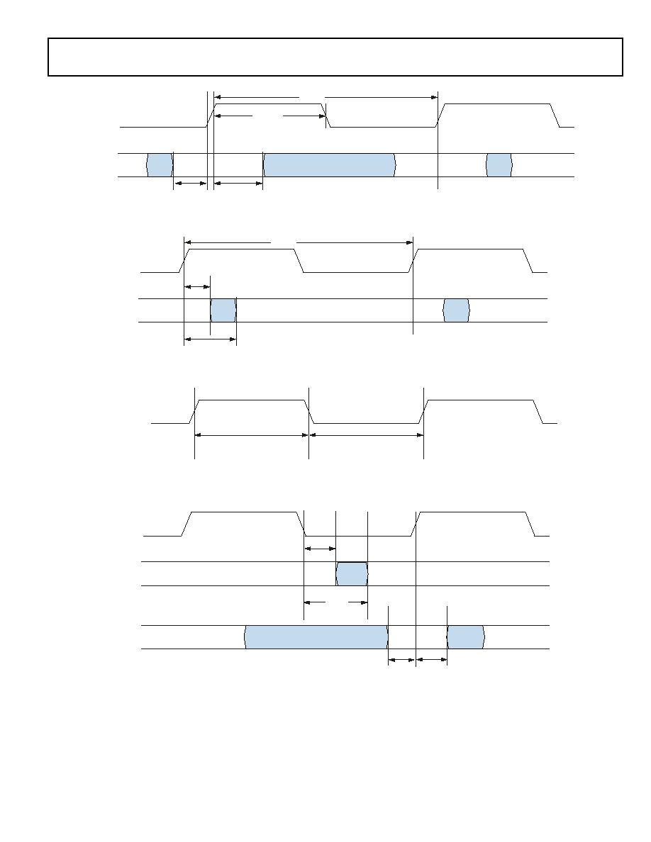
ADSP-BF534/ADSP-BF536/ADSP-BF537
Rev. B
|
Page 49 of 68
|
July 2006
Figure 31. 10/100 Ethernet MAC Controller Timing: RMII Receive Signal
Figure 32. 10/100 Ethernet MAC Controller Timing: RMII Transmit Signal
Figure 33. 10/100 Ethernet MAC Controller Timing: Asynchronous Signal
Figure 34. 10/100 Ethernet MAC Controller Timing: MII Station Management
ERxD1-0
ERxDV
ERxER
ERxCLK
t
REFCLK
t
ERXCLKIS
t
ERXCLKIH
t
REFCLKW
ETxD1-0
ETxEN
RMII REF_CLK
t
REFCLK
t
EREFCLKOH
t
EREFCLKOV
MII CRS, COL
t
ECRSH
t
ECRSL
t
ECOLH
t
ECOLL
MDIO (OUTPUT)
MDC (OUTPUT)
t
MDCOH
t
MDIOS
t
MDCIH
MDIO (INPUT)
t
MDCOV
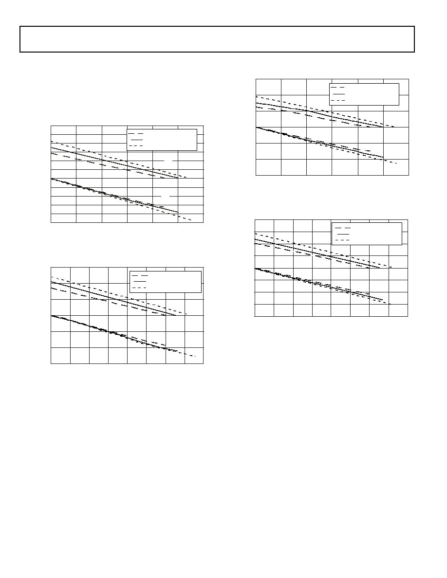
Rev. B
|
Page 50 of 68
|
July 2006
ADSP-BF534/ADSP-BF536/ADSP-BF537
OUTPUT DRIVE CURRENTS
Figure 35
through
Figure 46
show typical current-voltage char-
acteristics for the output drivers of the processors. The curves
represent the current drive capability of the output drivers as a
function of output voltage. See
Table 9 on Page 19
for informa-
tion about which driver type corresponds to a particular pin.
Figure 35. Drive Current A (Low V
DDEXT
)
Figure 36. Drive Current A (High V
DDEXT
)
0
S
O
U
R
C
E
C
U
R
R
E
N
T
(
m
A
)
SOURCE VOL TAGE (V)
0
0.5
1.0
1.5
2.0
2.5
3. 0
100
60
40
-
80
-
60
-
40
-
20
120
20
80
-
100
V
D DE XT
= 2.25V @ 95°C
V
D DE XT
= 2.50V @ 25°C
V
D DE XT
= 2.75V @ -40°C
V
OH
V
OL
0
S
O
U
R
C
E
C
U
R
R
E
N
T
(
m
A
)
SOURCE VOLTAGE (V)
0
0.5
1.0
1.5
2.0
2.5
3. 0
3.5
150
100
50
-
150
-
100
-
50
V
OL
V
O H
4.0
V
D D EX T
= 3.0V @ 95°C
V
D D EX T
= 3.3V @ 25°C
V
D D EX T
= 3.6V @ -40°C
Figure 37. Drive Current B (Low V
DDEXT
)
Figure 38. Drive Current B (High V
DDEXT
)
0
S
O
U
R
C
E
C
U
R
R
E
N
T
(
m
A
)
SOURCE VOLTAGE (V)
0
0.5
1. 0
1.5
2.0
2.5
3.0
150
100
-
150
V
OL
V
OH
-
100
-
50
50
V
D D EX T
= 2. 25V @ 95°C
V
DD E XT
= 2.50V @ 25° C
V
D DE XT
= 2.75V @ -40°C
0
S
O
U
R
C
E
C
U
R
R
E
N
T
(
m
A
)
SOURCE VOLTAGE (V)
0
0.5
1.0
1.5
2.0
2.5
3. 0
3.5
150
100
50
-
200
-
150
V
OL
V
O H
4.0
-
100
-
50
200
V
DD E XT
= 3.0V @ 95°C
V
DD E XT
= 3.3V @ 25°C
V
D D EX T
= 3.6V @ - 40°C
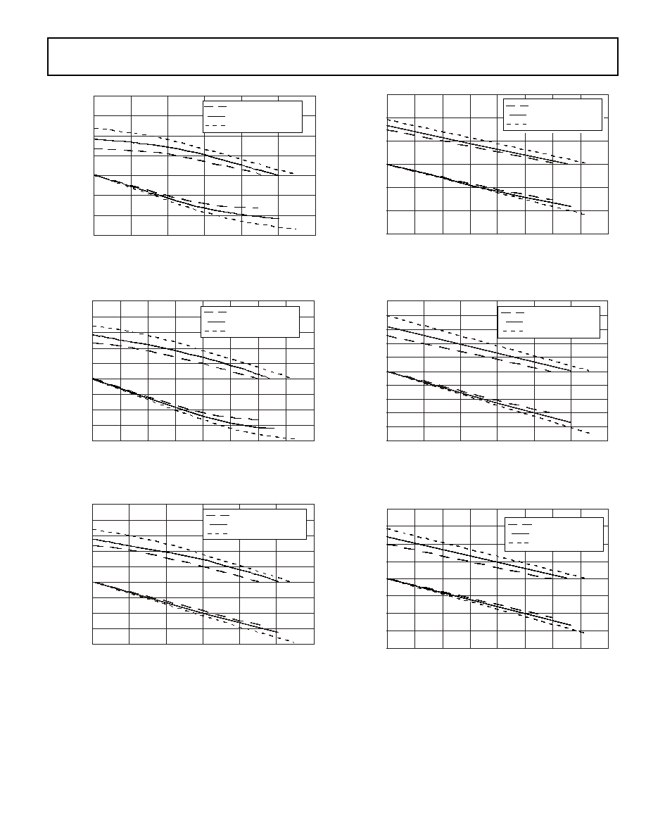
ADSP-BF534/ADSP-BF536/ADSP-BF537
Rev. B
|
Page 51 of 68
|
July 2006
Figure 39. Drive Current C (Low V
DDEXT
)
Figure 40. Drive Current C (High V
DDEXT
)
Figure 41. Drive Current D (Low V
DDEXT
)
0
S
O
U
R
C
E
C
U
R
R
E
N
T
(
m
A
)
SOURCE VOLTAGE (V)
0
0.5
1. 0
1.5
2.0
2.5
3.0
80
60
-
60
V
OL
V
OH
-
40
-
20
40
20
V
D D EXT
= 2.25V @ 95°C
V
D D EXT
= 2.50V @ 25°C
V
D D EX T
= 2.75V @ -40°C
0
S
O
U
R
C
E
C
U
R
R
E
N
T
(
m
A
)
SOURCE VOLTAGE (V)
0
0.5
1.0
1.5
2.0
2.5
3. 0
3.5
80
60
40
-
80
-
60
V
O L
V
OH
4.0
-
40
-
20
100
20
V
D D EX T
= 3. 0V @ 95° C
V
D D EX T
= 3. 3V @ 25° C
V
DD E XT
= 3.6V @ -40°C
0
S
O
U
R
C
E
C
U
R
R
E
N
T
(
m
A
)
SOURCE VOLTAGE (V)
0
0.5
1.0
1.5
2.0
2. 5
3.0
80
60
40
-
80
-
60
V
OL
V
OH
-
40
-
20
100
20
V
D DE XT
= 2.25V @ 95°C
V
D DE XT
= 2.50V @ 25°C
V
D D E XT
= 2.75V @ -40°C
Figure 42. Drive Current D (High V
DDEXT
)
Figure 43. Drive Current E (Low V
DDEXT
)
Figure 44. Drive Current E (High V
DDEXT
)
0
S
O
U
R
C
E
C
U
R
R
E
N
T
(
m
A
)
SOURCE VOLTAGE (V)
0
0.5
1.0
1.5
2.0
2.5
3. 0
3.5
100
50
-
150
V
OL
V
OH
4.0
-
100
-
50
150
V
D DE XT
= 3.0V @ 95° C
V
D DE XT
= 3.3V @ 25° C
V
DD E XT
= 3.6V @ -40°C
0
S
O
U
R
C
E
C
U
R
R
E
N
T
(
m
A
)
SOURCE VOL TAGE (V)
0
0.5
1.0
1.5
2.0
2.5
3. 0
40
20
10
-
40
-
30
V
OL
V
OH
V
D D EX T
= 2.25V @ 95° C
V
D D EX T
= 2.50V @ 25° C
V
D D EX T
= 2.75V @ - 40°C
-
20
-
10
50
30
-
50
0
S
O
U
R
C
E
C
U
R
R
E
N
T
(
m
A
)
SOURCE VOLTAGE (V)
0
0.5
1.0
1.5
2.0
2.5
3. 0
3.5
80
60
40
-
80
-
60
V
OL
V
O H
V
D D EX T
= 3. 0V @ 95°C
V
D D EX T
= 3. 3V @ 25°C
V
DD E XT
= 3.6V @ -40°C
4.0
-
40
-
20
20
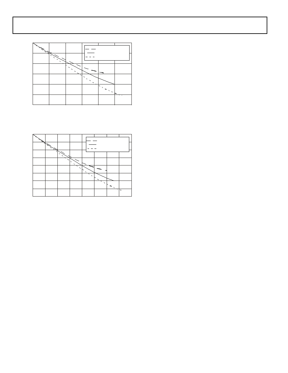
Rev. B
|
Page 52 of 68
|
July 2006
ADSP-BF534/ADSP-BF536/ADSP-BF537
Figure 45. Drive Current F (Low V
DDEXT
)
Figure 46. Drive Current F (High V
DDEXT
)
-
40
S
O
U
R
C
E
C
U
R
R
E
N
T
(
m
A
)
SOURCE VOLTAGE (V)
0
0.5
1.0
1.5
2.0
2.5
3.0
-
60
0
-
10
V
OL
-
20
-
30
-
50
V
DD E XT
= 2.25V @ 95°C
V
DD E XT
= 2.50V @ 25°C
V
D D EX T
= 2.75V @ -40° C
-
40
S
O
U
R
C
E
C
U
R
R
E
N
T
(
m
A
)
SOURCE VOLTAGE (V)
0
0. 5
1.0
1.5
2.0
2.5
3. 0
3.5
0
-
10
-
20
-
80
-
70
V
OL
4.0
-
60
-
50
-
30
V
D D EX T
= 3. 0V @ 95°C
V
D D EX T
= 3. 3V @ 25°C
V
D D EXT
= 3.6V @ -40°C

ADSP-BF534/ADSP-BF536/ADSP-BF537
Rev. B
|
Page 53 of 68
|
July 2006
POWER DISSIPATION
Total power dissipation has two components: one due to inter-
nal circuitry (P
INT
) and one due to the switching of external
output drivers (P
EXT
).
Table 40
shows the power dissipation for
internal circuitry (V
DDINT
).
Many operating conditions can affect power dissipation. System
designers should refer to EE-297: Estimating Power for the
ADSP-BF534/BF536/BF537 Blackfin Processors." This document
will provide detailed information for optimizing your design for
lowest power.
The external component of total power dissipation is caused by
the switching of output pins. Its magnitude depends on:
· The output voltage swing (V
DDEXT
).
· The output capacitance (C
0
) individual pins have to load.
· The maximum frequency (f
0
) at which individual pins
switch.
Furthermore, because I/O activity is usually not constant over
time, the external component of power dissipation is not a con-
stant value. Its peak value is best estimated by identifying
representative phases with the highest I/O activity and analyz-
ing output switching pin by pin. The following formula
calculates the average power for an analyzed period by accumu-
lating the power of all output pins.
The frequency f includes driving the load high and then back
low. For example: DATA150 pins can drive high and low at a
maximum rate of 1
÷
(2
t
SCLK
) while in SDRAM burst mode.
A typical power consumption can now be calculated for these
conditions by adding a typical internal power dissipation:
Note that the conditions causing a worst-case P
EXT
differ from
those causing a worst-case P
INT
. Maximum P
INT
cannot occur
while 100% of the output pins are switching from all ones (1s) to
all zeros (0s). Note, as well, that it is uncommon for an applica-
tion to have 100% or even 50% of the outputs switching
simultaneously.
Table 40. Internal Power Dissipation
Test Conditions
1
Parameter
f
CCLK
= 50 MHz
V
DDINT
= 0.8 V
f
CCLK
= 400 MHz
V
DDINT
=1.0 V
f
CCLK
= 400 MHz
V
DDINT
=1.2 V
Unit
I
DDTYP
2
26
130
160
mA
I
DDSLEEP
3,
4
16
30
37
mA
I
DDDEEPSLEEP
3
14
25
31
mA
I
DDHIBERNATE
4
50
50
50
A
I
DDRTC
5
30
30
30
A
Parameter
f
CCLK
= 250 MHz
V
DDINT
= 0.8 V
f
CCLK
= 500 MHz
V
DDINT
=1.2 V
Unit
I
DDTYP
2
65
190
mA
I
DDSLEEP
3, 4
16
37
mA
I
DDDEEPSLEEP
3
14
31
mA
I
DDHIBERNATE
4
50
50
A
I
DDRTC
5
30
30
A
Parameter
f
CCLK
= 600 MHz
V
DDINT
= 1.2 V
Unit
I
DDTYP
2
220
mA
I
DDSLEEP
3, 4
37
mA
I
DDDEEPSLEEP
3
31
mA
I
DDHIBERNATE
4
50
A
I
DDRTC
5
30
A
1
I
DD
data is specified for typical process parameters. All data at 25
°
C.
2
Processor executing 75% dual MAC, 25% ADD with moderate data bus activity.
3
See the ADSP-BF537 Blackfin Processor Hardware Reference Manual for definitions of sleep and deep sleep operating modes.
4
I
DDHIBERNATE
is measured @ V
DDEXT
= 3.65 V with the core voltage regulator off (V
DDINT
= 0 V).
5
Measured at V
DDRTC
= 3.3 V at 25
°
C.
P
EXT
V
DDEXT
2
C
0
f
0
×
=
P
TOTAL
P
EXT
I
DD
V
DDINT
×
(
)
+
=
Rev. B
|
Page 54 of 68
|
July 2006
ADSP-BF534/ADSP-BF536/ADSP-BF537
TEST CONDITIONS
All timing parameters appearing in this data sheet were
measured under the conditions described in this section.
Output Enable Time
Output pins are considered to be enabled when they have made
a transition from a high impedance state to the point when they
start driving. The output enable time t
ENA
is the interval from
the point when a reference signal reaches a high or low voltage
level to the point when the output starts driving as shown in the
Output Enable/Disable diagram (
Figure 47
). The time
t
ENA_MEASURED
is the interval from when the reference signal
switches to when the output voltage reaches 2.0 V (output high)
or 1.0 V (output low). Time t
TRIP
is the interval from when the
output starts driving to when the output reaches the 1.0 V or
2.0 V trip voltage. Time t
ENA
is calculated as shown in
the equation:
If multiple pins (such as the data bus) are enabled, the measure-
ment value is that of the first pin to start driving.
Output Disable Time
Output pins are considered to be disabled when they stop driv-
ing, go into a high impedance state, and start to decay from their
output high or low voltage. The time for the voltage on the bus
to decay by
V is dependent on the capacitive load, C
L
and the
load current, I
L
. This decay time can be approximated by
the equation:
The output disable time t
DIS
is the difference between
t
DIS_MEASURED
and t
DECAY
as shown in
Figure 47
. The time
t
DIS_MEASURED
is the interval from when the reference signal
switches to when the output voltage decays
V from the mea-
sured output-high or output-low voltage. The time t
DECAY
is
calculated with test loads C
L
and I
L
, and with
V equal to 0.5 V.
Example System Hold Time Calculation
To determine the data output hold time in a particular system,
first calculate t
DECAY
using the equation given above. Choose
V
to be the difference between the processor's output voltage and
the input threshold for the device requiring the hold time. A
typical
V is 0.4 V. C
L
is the total bus capacitance (per data line),
and I
L
is the total leakage or three-state current (per data line).
The hold time is t
DECAY
plus the minimum disable time (for
example, t
DSDAT
for an SDRAM write cycle).
t
ENA
t
ENA_MEASURED
t
TRIP
=
t
DECAY
C
L
V
(
)
I
L
/
=
Figure 47. Output Enable/Disable
Figure 48. Equivalent Device Loading for AC Measurements
(Includes All Fixtures)
Figure 49. Voltage Reference Levels for AC Measurements (Except
Output Enable/Disable)
REFERENCE
SIGNAL
t
DIS
OUTPUT STARTS DRIVING
V
OH
(MEASURED)
V
V
OL
(MEASURED) +
V
t
DIS_MEASURED
V
OH
(MEASURED)
V
OL
(MEASURED)
V
TRIP
(HIGH)
V
OH
(MEASURED)
V
OL
(MEASURED)
HIGH IMPEDANCE STATE
OUTPUT STOPS DRIVING
t
ENA
t
DECAY
t
ENA_MEASURED
t
TRIP
V
TRIP
(LOW)
V
LOAD
30pF
TO
OUTPUT
PIN
50
INPUT
OR
OUTPUT
V
MEAS
V
M EAS

ADSP-BF534/ADSP-BF536/ADSP-BF537
Rev. B
|
Page 55 of 68
|
July 2006
Capacitive Loading
Output delays and holds are based on standard capacitive loads:
30 pF on all pins (see
Figure 48
).
Figure 50
through
Figure 59 on
Page 57
show how output rise time varies with capacitance. The
delay and hold specifications given should be derated by a factor
derived from these figures. The graphs in these figures may not
be linear outside the ranges shown.
Figure 50. Typical Output Delay or Hold for Driver A at V
DDEXT
Min
Figure 51. Typical Output Delay or Hold for Driver A at V
DDEXT
Max
ABE0
(1
33
MHz DRIVER), V
DDEXT
(MIN)
= 2.25V, TEMPERATURE =
8
5°C
LOAD CAPACITANCE (pF)
RI
S
E TIME
RI
S
E
AND
F
ALL
TIME
n
s
(10%
t0
90%)
14
12
10
8
6
4
2
0
0
50
100
150
200
250
FALL TIME
ABE0
(1
33
MHz DRIVER), V
DDEXT
(MAX)
=
3
.65V, TEMPERATURE =
8
5°C
LOAD CAPACITANCE (pF)
RI
S
E TIME
RI
S
E
AND
F
ALL
TIME
n
s
(10%
to
90%)
12
10
8
6
4
2
0
0
50
100
150
200
250
FALL TIME
Figure 52. Typical Output Delay or Hold for Driver B at V
DDEXT
Min
Figure 53. Typical Output Delay or Hold for Driver B at V
DDEXT
Max
CLKOUT (CLKOUT DRIVER), V
DDEXT
(MIN)
= 2.25V, TEMPERATURE =
8
5°C
LOAD CAPACITANCE (pF)
RI
S
E TIME
RI
S
E
AND
F
ALL
TIME
n
s
(10%
to
90%)
12
10
8
6
4
2
0
0
50
100
150
200
250
FALL TIME
CLKOUT (CLKOUT DRIVER), V
DDEXT
(MAX)
=
3
.65V, TEMPERATURE =
8
5°C
LOAD CAPACITANCE (pF)
RI
S
E TIME
RI
S
E
AND
F
ALL
TIME
n
s
(10%
to
90%)
10
9
8
7
6
5
4
3
2
1
0
0
50
100
150
200
250
FALL TIME
Rev. B
|
Page 56 of 68
|
July 2006
ADSP-BF534/ADSP-BF536/ADSP-BF537
Figure 54. Typical Output Delay or Hold for Driver C at V
DDEXT
Min
Figure 55. Typical Output Delay or Hold for Driver C at V
DDEXT
Max
PF9 (
33
MHz DRIVER), V
DDEXT
(MIN)
= 2.25V, TEMPERATURE =
8
5°C
LOAD CAPACITANCE (pF)
RI
S
E TIME
RI
S
E
AND
F
ALL
TIME
n
s
(10%
to
90%)
25
3
0
20
15
10
5
0
0
50
100
150
200
250
FALL TIME
PF9 (
33
MHz DRIVER), V
DDEXT
(MAX)
=
3
.65V, TEMPERATURE =
8
5°C
LOAD CAPACITANCE (pF)
RI
S
E TIME
RI
S
E
AND
F
ALL
TIME
n
s
(10%
to
90%)
20
1
8
16
14
12
10
8
6
4
2
0
0
50
100
150
200
250
FALL TIME
Figure 56. Typical Output Delay or Hold for Driver D at V
DDEXT
Min
Figure 57. Typical Output Delay or Hold for Driver D at V
DDEXT
Max
S
CK (66 MHz DRIVER), V
DDEXT
(MIN)
= 2.25V, TEMPERATURE =
8
5°C
LOAD CAPACITANCE (pF)
RI
S
E TIME
RI
S
E
AND
F
ALL
TIME
n
s
(10%
to
90%)
1
8
16
14
12
10
8
6
4
2
0
0
50
100
150
200
250
FALL TIME
S
CK (66 MHz DRIVER), V
DDEXT
(MAX)
=
3
.65V, TEMPERATURE =
8
5°C
LOAD CAPACITANCE (pF)
RI
S
E TIME
RI
S
E
AND
F
ALL
TIME
n
s
(10%
to
90%)
14
12
10
8
6
4
2
0
0
50
100
150
200
250
FALL TIME
ADSP-BF534/ADSP-BF536/ADSP-BF537
Rev. B
|
Page 57 of 68
|
July 2006
Figure 58. Typical Output Delay or Hold for Driver E at V
DDEXT
Min
Figure 59. Typical Output Delay or Hold for Driver E at V
DDEXT
Max
PH0 V
DDEXT
(MIN)
= 2.25V, TEMPERATURE =
8
5°C
LOAD CAPACITANCE (pF)
RI
S
E TIME
RI
S
E
AND
F
ALL
TIME
n
s
(10%
to
90%)
3
6
3
2
2
8
24
20
16
12
8
4
0
0
50
100
150
200
250
FALL TIME
PH0 V
DDEXT
(MAX)
=
3
.65V, TEMPERATURE =
8
5°C
LOAD CAPACITANCE (pF)
RI
S
E TIME
RI
S
E
AND
F
ALL
TIME
n
s
(10%
to
90%)
3
6
3
2
2
8
24
20
16
12
8
4
0
0
50
100
150
200
250
FALL TIME
Figure 60. Typical Output Delay or Hold for Driver F at V
DDEXT
Min
Figure 61. Typical Output Delay or Hold for Driver F at V
DDEXT
Max
PH0 V
DDEXT
(MAX)
=
3
.65V, TEMPERATURE =
8
5°C
LOAD CAPACITANCE (pF)
RI
S
E TIME
RI
S
E
AND
F
ALL
TIME
n
s
(10%
to
90%)
3
6
3
2
2
8
24
20
16
12
8
4
0
0
50
100
150
200
250
FALL TIME
PH0 V
DDEXT
(MAX)
=
3
.65V, TEMPERATURE =
8
5°C
LOAD CAPACITANCE (pF)
RI
S
E TIME
RI
S
E
AND
F
ALL
TIME
n
s
(10%
to
90%)
3
6
3
2
2
8
24
20
16
12
8
4
0
0
50
100
150
200
250
FALL TIME
Rev. B
|
Page 58 of 68
|
July 2006
ADSP-BF534/ADSP-BF536/ADSP-BF537
THERMAL CHARACTERISTICS
To determine the junction temperature on the application
printed circuit board use:
where:
T
J
= Junction temperature ( C)
T
CASE
= Case temperature ( C) measured by customer at top
center of package.
JT
= From
Table 41
P
D
= Power dissipation (see
Power Dissipation on Page 53
for
the method to calculate P
D
)
Values of
JA
are provided for package comparison and printed
circuit board design considerations.
JA
can be used for a first
order approximation of T
J
by the equation:
where:
T
A
= Ambient temperature ( C)
Values of
JC
are provided for package comparison and printed
circuit board design considerations when an external heat sink
is required.
Values of
JB
are provided for package comparison and printed
circuit board design considerations.
In
Table 41
through
Table 43
, airflow measurements comply
with JEDEC standards JESD51-2 and JESD51-6, and the junc-
tion-to-board measurement complies with JESD51-8. Test
board and thermal via design comply with JEDEC standards
JESD51-9 (BGA). The junction-to-case measurement complies
with MIL-STD-883 (Method 1012.1). All measurements use a
2S2P JEDEC test board.
Industrial applications using the 208-ball BGA package require
thermal vias, to an embedded ground plane, in the PCB. Refer to
JEDEC standard JESD51-9 for printed circuit board thermal
ball land and thermal via design information.
Table 41. Thermal Characteristics (182-Ball BGA)
Parameter
Condition
Typical
Unit
JA
0 linear m/s air flow
32.80
C/W
JMA
1 linear m/s air flow
29.30
C/W
JMA
2 linear m/s air flow
28.00
C/W
JB
20.10
C/W
JC
7.92
C/W
JT
0 linear m/s air flow
0.19
C/W
JT
1 linear m/s air flow
0.35
C/W
JT
2 linear m/s air flow
0.45
C/W
T
J
T
CASE
JT
P
D
×
(
)
+
=
T
J
T
A
JA
P
D
×
(
)
+
=
Table 42. Thermal Characteristics (208-Ball BGA Without
Thermal Vias in PCB)
Parameter
Condition
Typical
Unit
JA
0 linear m/s air flow
23.30
C/W
JMA
1 linear m/s air flow
20.20
C/W
JMA
2 linear m/s air flow
19.20
C/W
JB
13.05
C/W
JC
6.92
C/W
JT
0 linear m/s air flow
0.18
C/W
JT
1 linear m/s air flow
0.27
C/W
JT
2 linear m/s air flow
0.32
C/W
Table 43. Thermal Characteristics (208-Ball BGA with
Thermal Vias in PCB)
Parameter
Condition
Typical
Unit
JA
0 linear m/s air flow
22.60
C/W
JMA
1 linear m/s air flow
19.40
C/W
JMA
2 linear m/s air flow
18.40
C/W
JB
13.20
C/W
JC
6.85
C/W
JT
0 linear m/s air flow
0.16
C/W
JT
1 linear m/s air flow
0.27
C/W
JT
2 linear m/s air flow
0.32
C/W
ADSP-BF534/ADSP-BF536/ADSP-BF537
Rev. B
|
Page 59 of 68
|
July 2006
182-BALL MINI-BGA PINOUT
Table 44
lists the mini-BGA pinout by signal mnemonic.
Table 45 on Page 60
lists the mini-BGA pinout by ball number.
Table 44. 182-Ball Mini-BGA Ball Assignment (Alphabetically by Signal Mnemonic)
Mnemonic
Ball No.
Mnemonic
Ball No.
Mnemonic
Ball No.
Mnemonic
Ball No.
Mnemonic
Ball No.
ABE0
H13
CLKOUT
B14
GND
L6
PG8
E3
SRAS
D13
ABE1
H12
DATA0
M9
GND
L8
PG9
E4
SWE
D12
ADDR1
J14
DATA1
N9
GND
L10
PH0
C2
TCK
P2
ADDR10
M13
DATA10
N6
GND
M4
PH1
C3
TDI
M3
ADDR11
M14
DATA11
P6
GND
M10
PH10
B6
TDO
N3
ADDR12
N14
DATA12
M5
GND
P14
PH11
A2
TMS
N2
ADDR13
N13
DATA13
N5
NMI
B10
PH12
A3
TRST
N1
ADDR14
N12
DATA14
P5
PF0
M1
PH13
A4
VDDEXT
A1
ADDR15
M11
DATA15
P4
PF1
L1
PH14
A5
VDDEXT
C12
ADDR16
N11
DATA2
P9
PF10
J2
PH15
A6
VDDEXT
E6
ADDR17
P13
DATA3
M8
PF11
J3
PH2
C4
VDDEXT
E11
ADDR18
P12
DATA4
N8
PF12
H1
PH3
C5
VDDEXT
F4
ADDR19
P11
DATA5
P8
PF13
H2
PH4
C6
VDDEXT
F12
ADDR2
K14
DATA6
M7
PF14
H3
PH5
B1
VDDEXT
H5
ADDR3
L14
DATA7
N7
PF15
H4
PH6
B2
VDDEXT
H10
ADDR4
J13
DATA8
P7
PF2
L2
PH7
B3
VDDEXT
J11
ADDR5
K13
DATA9
M6
PF3
L3
PH8
B4
VDDEXT
J12
ADDR6
L13
EMU
M2
PF4
L4
PH9
B5
VDDEXT
K7
ADDR7
K12
GND
A10
PF5
K1
PJ0
C7
VDDEXT
K9
ADDR8
L12
GND
A14
PF6
K2
PJ1
B7
VDDEXT
L7
ADDR9
M12
GND
D4
PF7
K3
PJ10
D10
VDDEXT
L9
AMS0
E14
GND
E7
PF8
K4
PJ11
D11
VDDEXT
L11
AMS1
F14
GND
E9
PF9
J1
PJ2
B11
VDDEXT
P1
AMS2
F13
GND
F5
PG0
G1
PJ3
C11
VDDINT
E5
AMS3
G12
GND
F6
PG1
G2
PJ4
D7
VDDINT
E8
AOE
G13
GND
F10
PG10
D1
PJ5
D8
VDDINT
E10
ARDY
E13
GND
F11
PG11
D2
PJ6
C8
VDDINT
G10
ARE
G14
GND
G4
PG12
D3
PJ7
B8
VDDINT
K5
AWE
H14
GND
G5
PG13
D5
PJ8
D9
VDDINT
K8
BG
P10
GND
G11
PG14
D6
PJ9
C9
VDDINT
K10
BGH
N10
GND
H11
PG15
C1
RESET
C10
VDDRTC
B9
BMODE0
N4
GND
J4
PG2
G3
RTXO
A8
VROUT0
A13
BMODE1
P3
GND
J5
PG3
F1
RTXI
A9
VROUT1
B12
BMODE2
L5
GND
J9
PG4
F2
SA10
E12
XTAL
A11
BR
D14
GND
J10
PG5
F3
SCAS
C14
CLKBUF
A7
GND
K6
PG6
E1
SCKE
B13
CLKIN
A12
GND
K11
PG7
E2
SMS
C13
Rev. B
|
Page 60 of 68
|
July 2006
ADSP-BF534/ADSP-BF536/ADSP-BF537
Table 45. 182-Ball Mini-BGA Ball Assignment (Numerically by Ball Number)
Ball No.
Mnemonic
Ball No.
Mnemonic
Ball No.
Mnemonic
Ball No.
Mnemonic
Ball No.
Mnemonic
A1
VDDEXT
C10
RESET
F5
GND
J14
ADDR1
M9
DATA0
A2
PH11
C11
PJ3
F6
GND
K1
PF5
M10
GND
A3
PH12
C12
VDDEXT
F10
GND
K2
PF6
M11
ADDR15
A4
PH13
C13
SMS
F11
GND
K3
PF7
M12
ADDR9
A5
PH14
C14
SCAS
F12
VDDEXT
K4
PF8
M13
ADDR10
A6
PH15
D1
PG10
F13
AMS2
K5
VDDINT
M14
ADDR11
A7
CLKBUF
D2
PG11
F14
AMS1
K6
GND
N1
TRST
A8
RTXO
D3
PG12
G1
PG0
K7
VDDEXT
N2
TMS
A9
RTXI
D4
GND
G2
PG1
K8
VDDINT
N3
TDO
A10
GND
D5
PG13
G3
PG2
K9
VDDEXT
N4
BMODE0
A11
XTAL
D6
PG14
G4
GND
K10
VDDINT
N5
DATA13
A12
CLKIN
D7
PJ4
G5
GND
K11
GND
N6
DATA10
A13
VROUT0
D8
PJ5
G10
VDDINT
K12
ADDR7
N7
DATA7
A14
GND
D9
PJ8
G11
GND
K13
ADDR5
N8
DATA4
B1
PH5
D10
PJ10
G12
AMS3
K14
ADDR2
N9
DATA1
B2
PH6
D11
PJ11
G13
AOE
L1
PF1
N10
BGH
B3
PH7
D12
SWE
G14
ARE
L2
PF2
N11
ADDR16
B4
PH8
D13
SRAS
H1
PF12
L3
PF3
N12
ADDR14
B5
PH9
D14
BR
H2
PF13
L4
PF4
N13
ADDR13
B6
PH10
E1
PG6
H3
PF14
L5
BMODE2
N14
ADDR12
B7
PJ1
E2
PG7
H4
PF15
L6
GND
P1
VDDEXT
B8
PJ7
E3
PG8
H5
VDDEXT
L7
VDDEXT
P2
TCK
B9
VDDRTC
E4
PG9
H10
VDDEXT
L8
GND
P3
BMODE1
B10
NMI
E5
VDDINT
H11
GND
L9
VDDEXT
P4
DATA15
B11
PJ2
E6
VDDEXT
H12
ABE1
L10
GND
P5
DATA14
B12
VROUT1
E7
GND
H13
ABE0
L11
VDDEXT
P6
DATA11
B13
SCKE
E8
VDDINT
H14
AWE
L12
ADDR8
P7
DATA8
B14
CLKOUT
E9
GND
J1
PF9
L13
ADDR6
P8
DATA5
C1
PG15
E10
VDDINT
J2
PF10
L14
ADDR3
P9
DATA2
C2
PH0
E11
VDDEXT
J3
PF11
M1
PF0
P10
BG
C3
PH1
E12
SA10
J4
GND
M2
EMU
P11
ADDR19
C4
PH2
E13
ARDY
J5
GND
M3
TDI
P12
ADDR18
C5
PH3
E14
AMS0
J9
GND
M4
GND
P13
ADDR17
C6
PH4
F1
PG3
J10
GND
M5
DATA12
P14
GND
C7
PJ0
F2
PG4
J11
VDDEXT
M6
DATA9
C8
PJ6
F3
PG5
J12
VDDEXT
M7
DATA6
C9
PJ9
F4
VDDEXT
J13
ADDR4
M8
DATA3
ADSP-BF534/ADSP-BF536/ADSP-BF537
Rev. B
|
Page 61 of 68
|
July 2006
Figure 63
shows the top view of the mini-BGA ball configura-
tion.
Figure 62
shows the bottom view of the mini-BGA
ball configuration.
Figure 62. 182-Ball Mini-BGA Configuration (Top View)
A
B
C
D
E
F
G
H
J
K
L
M
N
P
1
2
3
4
5
6
7
8
9
10 11 12 13 14
V
DDINT
V
DDEXT
GND
I/O
KEY:
V
ROUT
V
DDRTC
Figure 63. 182-Ball Mini-BGA Configuration (Bottom View)
A
B
C
D
E
F
G
H
J
K
L
M
N
P
1
2
3
4
5
6
7
8
9
10
11
12
13
14
V
DDINT
V
DDEXT
GND
I/O
KEY:
V
ROUT
V
DDRTC
Rev. B
|
Page 62 of 68
|
July 2006
ADSP-BF534/ADSP-BF536/ADSP-BF537
208-BALL SPARSE MINI-BGA PINOUT
Table 46
lists the sparse mini-BGA pinout by signal mnemonic.
Table 47 on Page 63
lists the sparse mini-BGA pinout by ball
number.
Table 46. 208-Ball Sparse Mini-BGA Ball Assignment (Alphabetically by Signal Mnemonic)
Mnemonic
Ball No.
Mnemonic
Ball No.
Mnemonic
Ball No.
Mnemonic
Ball No.
Mnemonic
Ball No.
ABE0
P19
DATA12
Y4
GND
M13
PG6
E2
TDI
V1
ABE1
P20
DATA13
W4
GND
N9
PG7
D1
TDO
Y2
ADDR1
R19
DATA14
Y3
GND
N10
PG8
D2
TMS
U2
ADDR10
W18
DATA15
W3
GND
N11
PG9
C1
TRST
U1
ADDR11
Y18
DATA2
Y9
GND
N12
PH0
B4
VDDEXT
G7
ADDR12
W17
DATA3
W9
GND
N13
PH1
A5
VDDEXT
G8
ADDR13
Y17
DATA4
Y8
GND
P11
PH10
B9
VDDEXT
G9
ADDR14
W16
DATA5
W8
GND
V2
PH11
A10
VDDEXT
G10
ADDR15
Y16
DATA6
Y7
GND
W2
PH12
B10
VDDEXT
H7
ADDR16
W15
DATA7
W7
GND
W19
PH13
A11
VDDEXT
H8
ADDR17
Y15
DATA8
Y6
GND
Y1
PH14
B11
VDDEXT
J7
ADDR18
W14
DATA9
W6
GND
Y13
PH15
A12
VDDEXT
J8
ADDR19
Y14
EMU
T1
GND
Y20
PH2
B5
VDDEXT
K7
ADDR2
T20
GND
A1
NMI
C20
PH3
A6
VDDEXT
K8
ADDR3
T19
GND
A13
PF0
T2
PH4
B6
VDDEXT
L7
ADDR4
U20
GND
A20
PF1
R1
PH5
A7
VDDEXT
L8
ADDR5
U19
GND
B2
PF10
L2
PH6
B7
VDDEXT
M7
ADDR6
V20
GND
G11
PF11
K1
PH7
A8
VDDEXT
M8
ADDR7
V19
GND
H9
PF12
K2
PH8
B8
VDDEXT
N7
ADDR8
W20
GND
H10
PF13
J1
PH9
A9
VDDEXT
N8
ADDR9
Y19
GND
H11
PF14
J2
PJ0
B12
VDDEXT
P7
AMS0
M20
GND
H12
PF15
H1
PJ1
B13
VDDEXT
P8
AMS1
M19
GND
H13
PF2
R2
PJ10
B19
VDDEXT
P9
AMS2
G20
GND
J9
PF3
P1
PJ11
C19
VDDEXT
P10
AMS3
G19
GND
J10
PF4
P2
PJ2
D19
VDDINT
G12
AOE
N20
GND
J11
PF5
N1
PJ3
E19
VDDINT
G13
ARDY
J19
GND
J12
PF6
N2
PJ4
B18
VDDINT
G14
ARE
N19
GND
J13
PF7
M1
PJ5
A19
VDDINT
H14
AWE
R20
GND
K9
PF8
M2
PJ6
B15
VDDINT
J14
BG
Y11
GND
K10
PF9
L1
PJ7
B16
VDDINT
K14
BGH
Y12
GND
K11
PG0
H2
PJ8
B17
VDDINT
L14
BMODE0
W13
GND
K12
PG1
G1
PJ9
B20
VDDINT
M14
BMODE1
W12
GND
K13
PG10
C2
RESET
D20
VDDINT
N14
BMODE2
W11
GND
L9
PG11
B1
RTXO
A15
VDDINT
P12
BR
F19
GND
L10
PG12
A2
RTXI
A14
VDDINT
P13
CLKBUF
B14
GND
L11
PG13
A3
SA10
L20
VDDINT
P14
CLKIN
A18
GND
L12
PG14
B3
SCAS
K20
VDDRTC
A16
CLKOUT
H19
GND
L13
PG15
A4
SCKE
H20
VROUT0
E20
DATA0
Y10
GND
M9
PG2
G2
SMS
J20
VROUT1
F20
DATA1
W10
GND
M10
PG3
F1
SRAS
K19
XTAL
A17
DATA10
Y5
GND
M11
PG4
F2
SWE
L19
DATA11
W5
GND
M12
PG5
E1
TCK
W1
ADSP-BF534/ADSP-BF536/ADSP-BF537
Rev. B
|
Page 63 of 68
|
July 2006
Table 47
lists the sparse mini-BGA pinout by ball number.
Table 46 on Page 62
lists the sparse mini-BGA pinout by signal
mnemonic.
Table 47. 208-Ball Sparse Mini-BGA Ball Assignment (Numerically by Ball Number)
Ball No.
Mnemonic
Ball No.
Mnemonic
Ball No.
Mnemonic
Ball No.
Mnemonic
Ball No.
Mnemonic
A1
GND
C19
PJ11
J9
GND
M19
AMS1
W1
TCK
A2
PG12
C20
NMI
J10
GND
M20
AMS0
W2
GND
A3
PG13
D1
PG7
J11
GND
N1
PF5
W3
DATA15
A4
PG15
D2
PG8
J12
GND
N2
PF6
W4
DATA13
A5
PH1
D19
PJ2
J13
GND
N7
VDDEXT
W5
DATA11
A6
PH3
D20
RESET
J14
VDDINT
N8
VDDEXT
W6
DATA9
A7
PH5
E1
PG5
J19
ARDY
N9
GND
W7
DATA7
A8
PH7
E2
PG6
J20
SMS
N10
GND
W8
DATA5
A9
PH9
E19
PJ3
K1
PF11
N11
GND
W9
DATA3
A10
PH11
E20
VROUT0
K2
PF12
N12
GND
W10
DATA1
A11
PH13
F1
PG3
K7
VDDEXT
N13
GND
W11
BMODE2
A12
PH15
F2
PG4
K8
VDDEXT
N14
VDDINT
W12
BMODE1
A13
GND
F19
BR
K9
GND
N19
ARE
W13
BMODE0
A14
RTXI
F20
VROUT1
K10
GND
N20
AOE
W14
ADDR18
A15
RTXO
G1
PG1
K11
GND
P1
PF3
W15
ADDR16
A16
VDDRTC
G2
PG2
K12
GND
P2
PF4
W16
ADDR14
A17
XTAL
G7
VDDEXT
K13
GND
P7
VDDEXT
W17
ADDR12
A18
CLKIN
G8
VDDEXT
K14
VDDINT
P8
VDDEXT
W18
ADDR10
A19
PJ5
G9
VDDEXT
K19
SRAS
P9
VDDEXT
W19
GND
A20
GND
G10
VDDEXT
K20
SCAS
P10
VDDEXT
W20
ADDR8
B1
PG11
G11
GND
L1
PF9
P11
GND
Y1
GND
B2
GND
G12
VDDINT
L2
PF10
P12
VDDINT
Y2
TDO
B3
PG14
G13
VDDINT
L7
VDDEXT
P13
VDDINT
Y3
DATA14
B4
PH0
G14
VDDINT
L8
VDDEXT
P14
VDDINT
Y4
DATA12
B5
PH2
G19
AMS3
L9
GND
P19
ABE0
Y5
DATA10
B6
PH4
G20
AMS2
L10
GND
P20
ABE1
Y6
DATA8
B7
PH6
H1
PF15
L11
GND
R1
PF1
Y7
DATA6
B8
PH8
H2
PG0
L12
GND
R2
PF2
Y8
DATA4
B9
PH10
H7
VDDEXT
L13
GND
R19
ADDR1
Y9
DATA2
B10
PH12
H8
VDDEXT
L14
VDDINT
R20
AWE
Y10
DATA0
B11
PH14
H9
GND
L19
SWE
T1
EMU
Y11
BG
B12
PJ0
H10
GND
L20
SA10
T2
PF0
Y12
BGH
B13
PJ1
H11
GND
M1
PF7
T19
ADDR3
Y13
GND
B14
CLKBUF
H12
GND
M2
PF8
T20
ADDR2
Y14
ADDR19
B15
PJ6
H13
GND
M7
VDDEXT
U1
TRST
Y15
ADDR17
B16
PJ7
H14
VDDINT
M8
VDDEXT
U2
TMS
Y16
ADDR15
B17
PJ8
H19
CLKOUT
M9
GND
U19
ADDR5
Y17
ADDR13
B18
PJ4
H20
SCKE
M10
GND
U20
ADDR4
Y18
ADDR11
B19
PJ10
J1
PF13
M11
GND
V1
TDI
Y19
ADDR9
B20
PJ9
J2
PF14
M12
GND
V2
GND
Y20
GND
C1
PG9
J7
VDDEXT
M13
GND
V19
ADDR7
C2
PG10
J8
VDDEXT
M14
VDDINT
V20
ADDR6
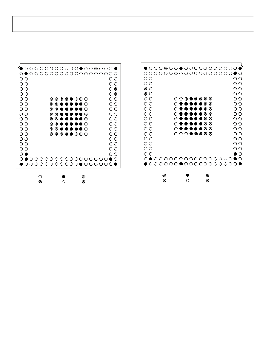
Rev. B
|
Page 64 of 68
|
July 2006
ADSP-BF534/ADSP-BF536/ADSP-BF537
Figure 64
shows the top view of the sparse mini-BGA ball con-
figuration.
Figure 65
shows the bottom view of the sparse mini-
BGA ball configuration.
Figure 64. 208-Ball Mini-BGA Configuration (Top View)
A
B
C
D
E
F
G
H
J
K
L
M
N
P
1
2
3
4
5
6
7
8
9
10 11 12 13 14
16 17 18 19 20
15
V
DDINT
V
DDEXT
GND
I/O
KEY:
V
ROUT
V
DDRTC
R
T
U
V
W
Y
Figure 65. 208-Ball Mini-BGA Configuration (Bottom View)
A
B
C
D
E
F
G
H
J
K
L
M
N
P
20 19 18 17 16 15 14 13 12 11 10
9
8
7
5
4
3
2
1
6
V
DDINT
V
DDEXT
GND
I/O
KEY:
V
ROUT
V
DDRTC
R
T
U
V
W
Y
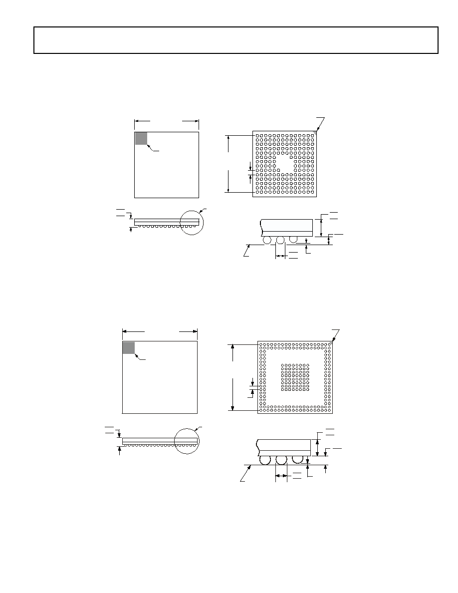
ADSP-BF534/ADSP-BF536/ADSP-BF537
Rev. B
|
Page 65 of 68
|
July 2006
OUTLINE DIMENSIONS
Dimensions in
Figure 66
and
Figure 67
are shown in
millimeters.
Figure 66. 182-Ball Mini-BGA (BC-182)
Figure 67. 208-Ball Sparse Mini-BGA (BC-208-2)
0.80
BSC
TYP
DETAIL A
DETAIL A
0.50
0.45
0.40
1.31
1.21
1.10
10.40
BSC
SQ
A
B
C
D
E
F
G
H
J
K
L
M
N
P
14
13
12
11
10
8
7
6
3
2
1
9
5
4
A1 CORNER
INDEX AREA
TOP VIEW
BOTTOM VIEW
1.70
1.56
1.35
12.00 BSC SQ
(BALL
DIAMETER)
SEATING
PLANE
0.35 NOM
0.25 MIN
0.12
COPLANARITY
PIN A1
INDICATOR
LOCATION
NOTES:
1. DIMENSIONS ARE IN MILLIMETERS.
2. COMPLIANT TO JEDEC STANDARD MO-205-AE,
EXCEPT FOR BALL DIAMETER.
3. CENTER DIMENSIONS ARE NOMINAL.
4.
THE ACTUAL POSITION OF THE BALL GRID IS
WITHIN 0.15 OF ITS IDEAL POSITION RELATIVE
TO THE PACKAGE EDGES.
0.80
BSC
TYP
A
B
C
D
E
F
G
H
J
K
L
M
N
P
R
T
U
V
W
Y
15
14
17
16
19
18
20
13
12
11
10
9
8
7
6
5
4
3
2
1
BOTTOM VIEW
15.20
BSC
SQ
A1 CORNER
INDEX AREA
0.12
COPLANARITY
DETAIL A
0.50
0.45
0.40
(BALL
DIAMETER)
0.35 NOM
0.25 MIN
TOP VIEW
PIN A1
INDICATOR
LOCATION
DETAIL A
17.00 BSC SQ
SEATING
PLANE
1.70
1.56
1.35
1.31
1.21
1.10
NOTES:
1. DIMENSIONS ARE IN MILLIMETERS.
2. COMPLIANT TO JEDEC STANDARD MO-205-AM,
EXCEPT FOR BALL DIAMETER.
3. CENTER DIMENSIONS ARE NOMINAL.
4. THE ACTUAL POSITION OF THE BALL GRID IS
WITHIN 0.15 OF ITS IDEAL POSITION RELATIVE
TO THE PACKAGE EDGES.
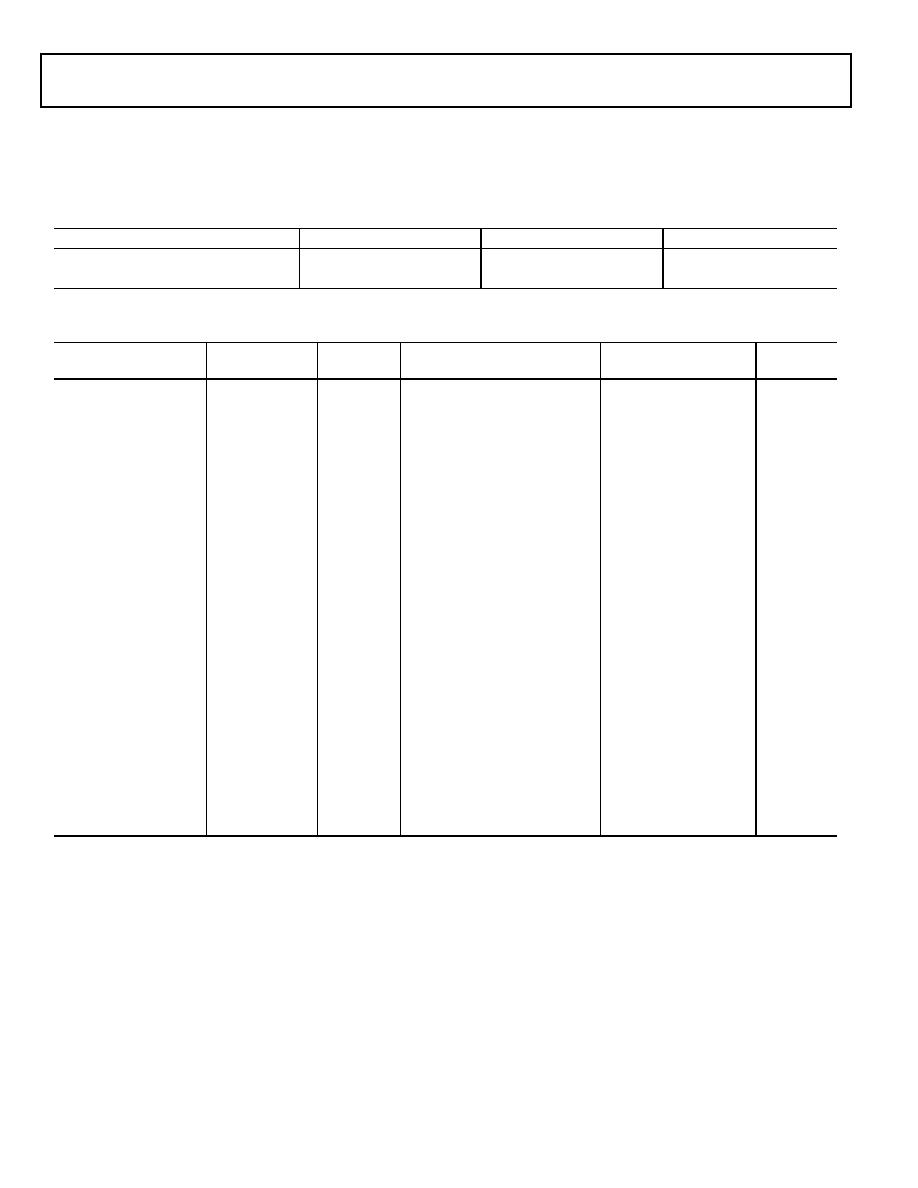
Rev. B
|
Page 66 of 68
|
July 2006
ADSP-BF534/ADSP-BF536/ADSP-BF537
SURFACE MOUNT DESIGN
The following table is provided as an aide to PCB design. For
industry-standard design recommendations, refer to IPC-7351,
Generic Requirements for Surface Mount Design and Land Pat-
tern Standard.
ORDERING GUIDE
Package
Ball Attach Type
Solder Mask Opening
Ball Pad Size
182-Ball Mini-BGA (BC-182)
Solder Mask Defined
0.40 mm diameter
0.55 mm diameter
208-Ball Sparse Mini-BGA (BC-208-2)
Solder Mask Defined
0.40 mm diameter
0.55 mm diameter
Model
Temperature
Range
1
1
Referenced temperature is ambient temperature.
Speed Grade
(Max)
Operating Voltage (Nominal)
Package Description
Package
Option
ADSP-BF534BBC-4A 40
°
C to +85
°
C
400 MHz
1.2 V internal, 2.5 V or 3.3 V I/O
182-Ball Mini-BGA
BC-182
ADSP-BF534BBCZ-4A
2
2
Z = Pb-free part.
40
°
C to +85
°
C
400 MHz
1.2 V internal, 2.5 V or 3.3 V I/O
182-Ball Mini-BGA
BC-182
ADSP-BF534BBC-5A
40
°
C to +85
°
C
500 MHz
1.26 V internal, 2.5 V or 3.3 V I/O
182-Ball Mini-BGA
BC-182
ADSP-BF534BBCZ-5A
2
40
°
C to +85
°
C
500 MHz
1.26 V internal, 2.5 V or 3.3 V I/O
182-Ball Mini-BGA
BC-182
ADSP-BF534BBCZ-4B
2
40
°
C to +85
°
C
400 MHz
1.2 V internal, 2.5 V or 3.3 V I/O
208-Ball Sparse Mini-BGA
BC-208-2
ADSP-BF534BBCZ-5B
2
40
°
C to +85
°
C
500 MHz
1.26 V internal, 2.5 V or 3.3 V I/O
208-Ball Sparse Mini-BGA
BC-208-2
ADSP-BF534YBCZ-4B
2
40
°
C to +105
°
C
400 MHz
1.2 V internal, 2.5 V or 3.3 V I/O
208-Ball Sparse Mini-BGA
BC-208-2
ADSP-BF534WYBCZ-4B
2,
3
3
The W in the model number signifies that a version of this product is available for use in automotive applications. Contact your local ADI sales office for complete ordering
information.
40
°
C to +105
°
C
400 MHz
1.2 V internal, 2.5 V or 3.3 V I/O
208-Ball Sparse Mini-BGA
BC-208-2
ADSP-BF534WBBCZ-4A
2, 3
40
°
C to +85
°
C
400 MHz
1.2 V internal, 2.5 V or 3.3 V I/O
182-Ball Mini-BGA
BC-182
ADSP-BF534WBBCZ-4B
2, 3
40
°
C to +85
°
C
400 MHz
1.2 V internal, 2.5 V or 3.3 V I/O
208-Ball Sparse Mini-BGA
BC-208-2
ADSP-BF534WBBCZ-5B
2, 3
40
°
C to +85
°
C
500 MHz
1.26 V internal, 2.5 V or 3.3 V I/O
208-Ball Sparse Mini-BGA
BC-208-2
ADSP-BF536BBC-3A 40
°
C to +85
°
C
300 MHz
1.2 V internal, 2.5 V or 3.3 V I/O
182-Ball Mini-BGA
BC-182
ADSP-BF536BBCZ-3A
2
40
°
C to +85
°
C
300 MHz
1.2 V internal, 2.5 V or 3.3 V I/O
182-Ball Mini-BGA
BC-182
ADSP-BF536BBC-4A
40
°
C to +85
°
C
400 MHz
1.2 V internal, 2.5 V or 3.3 V I/O
182-Ball Mini-BGA
BC-182
ADSP-BF536BBCZ-4A
2
40
°
C to +85
°
C
400 MHz
1.2 V internal, 2.5 V or 3.3 V I/O
182-Ball Mini-BGA
BC-182
ADSP-BF536BBCZ-3B
2
40
°
C to +85
°
C
300 MHz
1.2 V internal, 2.5 V or 3.3 V I/O
208-Ball Sparse Mini-BGA
BC-208-2
ADSP-BF536BBCZ-4B
2
40
°
C to +85
°
C
400 MHz
1.2 V internal, 2.5 V or 3.3 V I/O
208-Ball Sparse Mini-BGA
BC-208-2
ADSP-BF537BBC-5A
40
°
C to +85
°
C
500 MHz
1.26 V internal, 2.5 V or 3.3 V I/O
182-Ball Mini-BGA
BC-182
ADSP-BF537BBCZ-5A
2
40
°
C to +85
°
C
500 MHz
1.26 V internal, 2.5 V or 3.3 V I/O
182-Ball Mini-BGA
BC-182
ADSP-BF537KBC-6A
0
°
C to 70
°
C
600 MHz
1.26 V internal, 2.5 V or 3.3 V I/O
182-Ball Mini-BGA
BC-182
ADSP-BF537KBCZ-6A
2
0
°
C to 70
°
C
600 MHz
1.26 V internal, 2.5 V or 3.3 V I/O
182-Ball Mini-BGA
BC-182
ADSP-BF537BBCZ-5B
2
40
°
C to +85
°
C
500 MHz
1.26 V internal, 2.5 V or 3.3 V I/O
208-Ball Sparse Mini-BGA BC-208-2
ADSP-BF537KBCZ-6B
2
0
°
C to 70
°
C
600 MHz
1.26 V internal, 2.5 V or 3.3 V I/O
208-Ball Sparse Mini-BGA BC-208-2

ADSP-BF534/ADSP-BF536/ADSP-BF537
Rev. B
|
Page 67 of 68
|
July 2006

Rev. B
|
Page 68 of 68
|
July 2006
ADSP-BF534/ADSP-BF536/ADSP-BF537
©2006 Analog Devices, Inc. All rights reserved. Trademarks and
registered trademarks are the property of their respective owners.
D05317-0-6/06(B)
Document Outline