ADSP-21mod970-510 Data Sheet
REV. 0
Information furnished by Analog Devices is believed to be accurate and
reliable. However, no responsibility is assumed by Analog Devices for its
use, nor for any infringements of patents or other rights of third parties
which may result from its use. No license is granted by implication or
otherwise under any patent or patent rights of Analog Devices.
a
ADSP-21mod970-510
One Technology Way, P.O. Box 9106, Norwood, MA 02062-9106, U.S.A.
Tel: 781/329-4700
World Wide Web Site: http://www.analog.com
Fax: 781/326-8703
© Analog Devices, Inc., 1999
Multiport Internet Gateway Processor
Data Pump Solution
FEATURES
High Density
Implements Twelve Data Pump Channels in a Single
304-Ball PBGA Package with a 1.45 Square Inch
(961 sq. mm.) Footprint
Customizable Solution
Requires an External, OEM-Specific Device and Soft-
ware for Compression, Decompression, Error Correc-
tion, and AT Command Parsing
56 kbps HDLC
64 kbps HDLC
Data Modulations
ITU V.90 (30 kbps56 kbps)
K56FlexTM (30 kbps56 kbps)
ITU-T V.17: 14400 bps
ITU-T V.29: 9600 bps, 7200 bps
ITU-T V.27ter: 4800 bps, 2400 bps
ITU-T V.21 Channel 2: 300 bps
ITU-T V.34: 33600 bps2400 bps
ITU V.32bis: 14400 bps7200 bps
ITU V.32: 9600 bps, 4800 bps
ITU V.23, ITU V.22/V.22bis: 2400, 1200, 600 bps
ITU V.21: 300 bps, Bell 212A: 1200 bps
Bell 103: 300 bps
K56Flex is a trademark of Rockewell International and Lucent Technologies.
Initial/Start-Up Procedures:
ITU-T V.8, V.8bis
V.25
CNG Detection
Fax Modulations
Low Power
110 mW per Channel Typical Active
Low Power and Sleep Modes
On-Chip DS0/DS1 Interface
Full Function DMA Port
No External Memory Required
3.3 V Supply
Fully Upgradable RAM-Based Architecture
Fast Download
Full Image in 5 ms
High Speed 16-Bit Link Bus Port Provides Simple
Interface Between Controller and Data Pump
T1
E1
PRI
xDSL
ATM
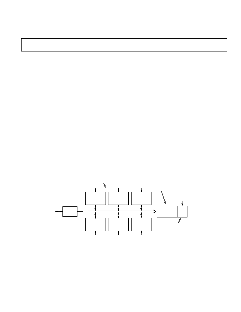
PORT LINK BUS
HOST
CONTROLLER
ADSP-21mod970
DATA PUMP FUNCTIONS
V.34/56kbps MODEM
HDLC PROTOCOL
V.34 ANNEX 12
V.17 FAX
TONE GENERATION
HOST FUNCTIONS
CALL CONTROL SIGNALING
AND SWITCHING,
MULTI-DSP CONTROL,
OVERLAY MANAGEMENT,
AND DATA TRANSFERS
PPP PACKETIZATION
T.30 CLASS 1, CLASS 2
FRAMER
SPO
DATA PUMP
CHANNEL 9 + 10
DMA
LAN
OR
INTERNET
EXTERNAL
CONTROLLER FUNCTIONS
V.42, V.42bis, MNP2-5
AT COMMAND PARSER
V.110, V.120
SPO
DATA PUMP
CHANNEL 5 + 6
DMA
SPO
DATA PUMP
CHANNEL 1 + 2
DMA
DMA
DATA PUMP
CHANNEL 11 + 12
SPO
DMA
DATA PUMP
CHANNEL 7 + 8
SPO
DMA
DATA PUMP
CHANNEL 3 + 4
SPO
Figure 1. ADSP-21mod970-510 Network Access System
REV. 0
ADSP-21mod970-510
2
Table I. Product Selection Guide
Number
Controller
DSP
Product
of Ports
Implementation
MIPs
Package
ADSP-21mod970-510 Data Pump Solution*
12
External to the device.
312
304 PBGA
Designed by the OEM.
ADSP-21mod970-110 Integrated Modem Solution*
6
Internal to the device.
312
304 PBGA
Included in the solution.
ADSP-21mod970-000 Device
Not Applicable.
312
304 PBGA
--
Stand-Alone Device.
NOTE
*Solution denotes a product offering that includes an ADSP-21mod970-000 device and DSP software from ADI for the supported functions.
PRODUCT SELECTION
Analog Devices has developed an entire family of Internet Gate-
way products that support a diverse set of applications. The
ADSP-21mod970-510 is a twelve-channel solution that includes
data pump functions and requires an external controller. The
ADSP-21mod970-110 is a six-channel solution that includes all
data pump and controller functions.
INTRODUCTION
The ADSP-21mod970-510 is a complete data pump solution in
a single device. Its Multiport Internet Gateway Processor architec-
ture is optimized for implementation of a twelve-channel,
V.34/56 kbps data pump. It combines a highly integrated DSP
processor with downloadable software. All data pump functions
are implemented on a single 1.45-square-inch device. This
package allows the highest port density while achieving the
lowest power consumption in a software upgradable platform.
The ADSP-21mod970 is designed for high density systems such
as remote access servers (see Figure 1). Its high performance
DSP core, large on-chip SRAM, TDM serials port, and 16-bit
DMA port provide efficient control and data communication with
minimal chip count. The modem software provides a number of
data modulations, such as V.34, 56 kbps PCM and ISDN with a
software upgrade path to future standards and new applications,
such as voice over network. The controller interface allows system
access to modem statistics such as call progress, connect speed and
modulation parameters such as retrain count and symbol rate.
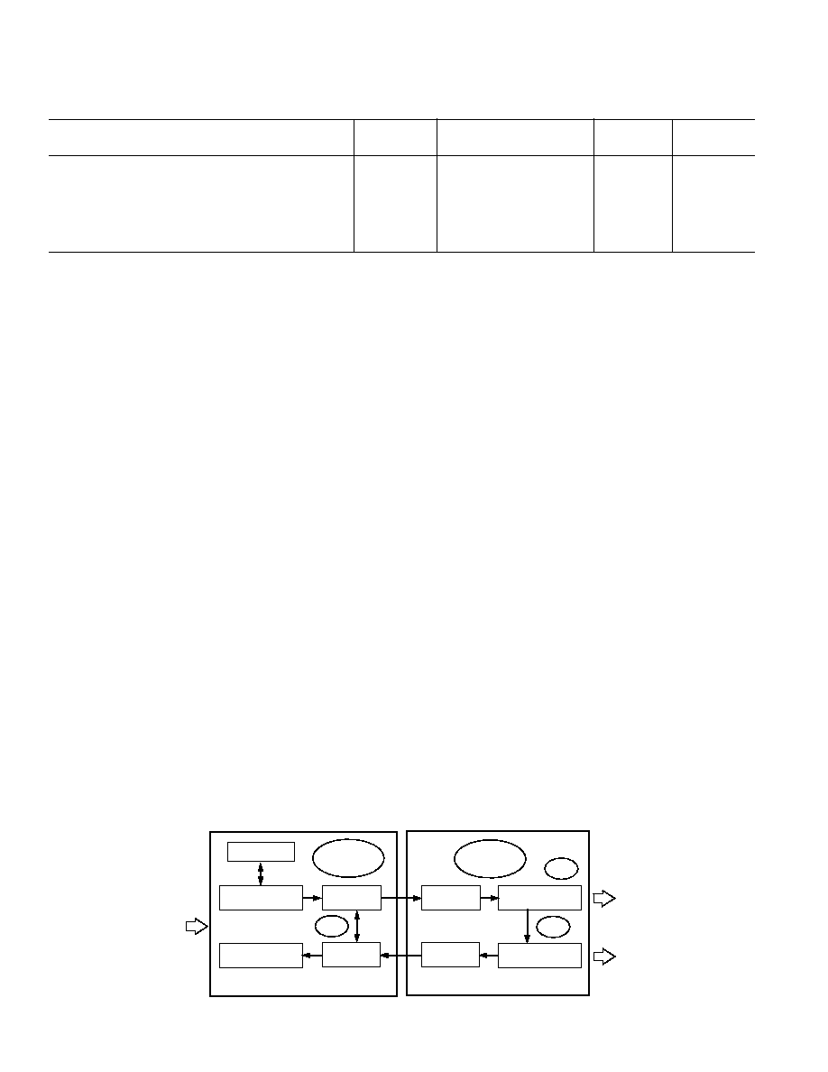
SYSTEM ARCHITECTURE
Communication between the controller processor and the mo-
dem processor can be divided into five basic functions:
1. Booting the DSP
2. Accessing mailbox locations to exchange control information
with the modem
3. Accessing data through FIFOs within the modem
4. Accessing statistics and telemetry data from the modem
5. Loading an image to the DSP upon request from the data
pump.
All of these functions are achieved through access of the modem
processor's internal memory by the controller.
ON-CHIP SRAM
The ADSP-21mod970 processor integrates 960K bytes of on-
chip memory. The modem data pump software, as well as data
storage, are contained in the on-chip SRAM. The SRAM cells
are a proprietary design by Analog Devices. These cells are
optimized for high speed digital signal processing and low power
consumption. The ADSP-21mod970 can be configured dy-
namically with software through the 16-bit DMA interface.
CONTROLLER OPERATIONS
There are three kinds of controller operations. These are:
· Boot Loading
· Mailbox Access
· Data FIFO Access
The following sections describe basic modem operations.
Boot Loading
The internal program memory (PM) and data memory (DM) of
the ADSP-21mod970 modem processor can be loaded with
modem code and data by a controller processor via the DMA
bus. The DMA port of the modem processor can be used to
load code and data into the processor's internal memory at any
time. The first requirement for loading code and data involves
boot loading the modem processor after reset.
DATA PUMP
STATE
MACHINE
MODULATOR
ECSM
LAP-M
TRANSMIT
DECOMPRESSION
AT PARSER
EXTERNAL CONTROLLER
CONTROL
SEQUENCER
ADSP-21mod970-510
DATA PUMP
DSM
LAP-M
RECEIVE
COMPRESSION
HDLC
TRANSMIT
HDLC
RECEIVE
DEMODULATOR
MSM
Figure 2. System Architecture

REV. 0
ADSP-21mod970-510
3
Modem code and data are provided in the form of an execut-
able image file. The image file consists of multiple modules of
code and data. The image file is divided up into 8K word pages.
Boot loading the modem processor involves loading some of
these pages of information into the internal program and data
memories of the modem processor.
During modem operation, the modem processor will make a
request to the controller for additional code and/or data. The
controller should respond by loading additional pages from the
image file. Each page of the image file contains a header, which
details:
· The Type of Memory (PM or DM)
· Starting Download Address
· Image File Page Number
The controller can locate the required page by parsing the
header of the image file and looking at the memory type and
page value.
The format of the image file is detailed in ADSP-21mod970-
510 API Guide. The controller loads the internal memory of the
modem processor with various 8K word pages at various times
during the modem's operation.
Starting at the download address, all subsequent memory loca-
tions must be loaded with either the value from the image file,
or zero.
After power is applied to the modem processor and the pro-
cessor is properly reset, it is ready to be boot loaded. The
controller boot loads the modem processor by extracting the
appropriate pages from the image file and loading the program
and data memory of the modem processor via the DMA port.
Table II shows the image file pages that are to be loaded at reset
into either PM or DM, along with the destination overlay page
within the modem processor's memory.
Table II. Memory Map Usage
Image File
Modem Overlay
Memory
Page
Page
PM
Startup A
0
DM
Startup A
0
PM
Startup B
4
DM
Startup B
4
PM
Resampling Filters
5
DM
State Machine
5
PM
OS
Nonpaged Section Address
0x00000x1FFF
DM
OS
Nonpaged Section Address
0x20000x3FDF
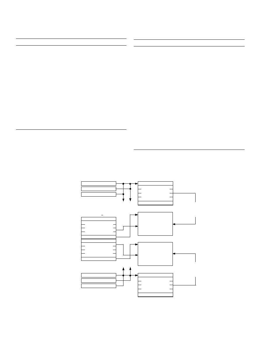
This loads the start-up code (overlay page 0 for Modem A and
overlay page 4 for Modem B) and the rate converter filters into
PM overlay page 5. DM overlay page 5 is used by the modem
code for digital echo canceller buffers and state machine tables.
One-half of the page is reserved for Modem A and the other half
is for Modem B. Code and data loaded into the nonpaged area
of memory is common to all modulations. When PM address
0x0000 is loaded, the DSP starts execution. Figure 3 illustrates
how the Program Memory overlay pages are used for the two
modems called Application A and Application B.
0x0000
0x1FFF
8K 24-BIT
0x2000
0x3FFF
PMOVLY = 0
8K 24-BIT
SHELL (OS)
VCORE (AGC, ALTERATIONS, BIT PROCESSING,
BIT CORRELATION, ECHO CANCELLATION,
EQUALIZER, TIMING RECOVERY, UP-CONVERTER,
MAPPER, DATA CONVERTER, VITERBI)
HDLC AND V.14 LIBRARY
(FIFO UTILITIES, CRC, FFT, PLL, SIN, DIV,
ROTATE, FIR)
APPLICATION "A"
(ANY ONE OF V.34, V.32/bis, 56K, V.22/bis, ISDN, ETC.)
APPLICATION "B"
RESAMPLING FILTERS
PROGRAM
MEMORY
PMOVLY = 4
8K 24-BIT
PMOVLY = 5
8K 24-BIT
Figure 3. Program Memory Overlay Pages
In order for the controller to locate the appropriate image file
pages properly, it will need to parse the image file for PM (@PA)
or DM (@DA) header characters. The controller then needs to
parse the next 24-bit value and check Bits 13 through 23 for the
page number. If the page number encountered is the image file
page number required, the controller can begin transferring the
data that follows. In the case of a boot load after reset, PM
address 0x0000 must be loaded last. If the page number en-
countered is not the image file page number required, the con-
troller should proceed to check the next section header.
Mailbox Access
Once the modem processor has been boot loaded and is run-
ning, the controller can communicate with the modem proces-
sor via a set of mailbox registers, internal memory locations of
the modem processor. Mailboxes are small, fixed memory blocks
used to communicate commands and results between the mod-
ules of the modem and the external host/controller. The exter-
nal host/controller is also interchangeably referred to as the
Sequencer. The modem is also interchangeably referred to as the
Data Pump State Machine (DPSM).
Mailbox Description
There is a mailbox for controller (Sequencer)-to-DSP modem
communications (SEQ_DPSM) and a mailbox for DPSM modem-
to-controller communications (DPSM_SEQ). The mailbox
actually represents a set of locations. There are sixteen consecu-
tive locations to each mailbox. The first location is used for the
command; the remaining locations hold optional arguments.
The starting addresses of the mailboxes within the modem
processor's internal memory are referred to symbolically. The
actual address may change from one software revision to the
next. To find the memory address, you will need to extract the
information from the symbol table supplied with the modem
software. The symbols to look for are Seq_Dpsm and Dpsm_Seq.
In addition, there is a mailbox for error control (V.42, MNPTM)
to bit processing (HDLC) communications (Ec_Bp) and a
mailbox for bit processing (HDLC) to error control (V.42,
MNP) communications (Bp_Ec).
The controller writes commands and indications in the
SEQ_DPSM mailbox locations and the DPSM clears (sets to
zero) the mailbox to acknowledge receipt. This is also true in
the reverse order for the DPSM_SEQ mailbox locations. Refer
to the API documentation supplied with the modem software
for the most accurate list of modem commands.
MNP is a trademark of Compaq Computer Corporation.
REV. 0
ADSP-21mod970-510
4
Table III. Modem Commands--Modem-to-Controller
Modem-to-Controller Commands
DPSM_SEQ_I_NEED_CODE
DPSM_SEQ_I_CONNECTED
DPSM_SEQ_I_FAILED_CONNECT
DPSM_SEQ_I_FLAGS_FOUND
DPSM_SEQ_I_FFT_RESULTS
DPSM_SEQ_I_FTH_FLAGS_DONE
DPSM_SEQ_C_LOST_CARRIER
DPSM_SEQ_I_END_OF_RCV_DATA
DPSM_SEQ_I_END_OF_TRANSMISSION
DPSM_SEQ_I_DRAIN_DONE
DPSM_SEQ_I_FFT_COMPLETE
DPSM_SEQ_I_FLAGS_FOUND
DPSM_SEQ_I_FOUND_CNG
DPSM_SEQ_I_CED_DONE
DPSM_SEQ_I_READY_TO_XMT
DPSM_SEQ_I_READY_TO_DRAIN
DPSM_SEQ_I_DTMF_REPORT
Table IV. Modem Commands--Controller-to-Modem
Controller-to-Modem Commands
SEQ_DPSM_C_ABORT
SEQ_DPSM_C_DISCONNECT
SEQ_DPSM_C_GET_ENERGY_RANGES
SEQ_DPSM_C_V110_CALL
SEQ_DPSM_C_V110_ANSWER
SEQ_DPSM_C_V8_ANSWER
SEQ_DPSM_C_DTMF_ANSWER
SEQ_DPSM_C_V8_CALL
SEQ_DPSM_C_T30_CALL
SEQ_DPSM_C_FRH
SEQ_DPSM_C_FTH
SEQ_DPSM_C_V29_TRNSONLY
SEQ_DPSM_C_V29_RCVONLY
SEQ_DPSM_C_V27_TRNSONLY
SEQ_DPSM_C_V27_RCVONLY
SEQ_DPSM_C_V17_RCVONLY
SEQ_DPSM_C_R_V17_RCVONLY
SEQ_DPSM_C_R_V17_TRNSONLY
SEQ_DPSM_C_V17_TRNSONLY
SEQ_DPSM_C_DONE_LOAD_IMAGE
SEQ_DPSM_I_ETX
The recipient clears the mailbox by writing a 0 to the mailbox.
The sender should check that the mailbox contains a 0 before
writing to it. When a 0 value is written into the mailbox, it acts
as an indicator that the previous command has been processed.
LENGTH IN WORDS
READ WORD POINTER
READ BIT POINTER
WRITE WORD POINTER
WRITE BIT POINTER
FIFO BASE ADDRESS
LENGTH IN WORDS
READ WORD POINTER
READ BIT POINTER
WRITE WORD POINTER
WRITE BIT POINTER
FIFO BASE ADDRESS
CONTROL WORD
FIFO FOR TRANSMIT
(DOWNSTREAM)
DATA
Tx WRITE IDX
Tx READ IDX
EC Tx FIFO
FIFODB
TRANSMIT
(DOWNSTREAM)
FIFO BUFFER
RECEIVE
(UPSTREAM)
FIFO BUFFER
CONTROLLER
WRITES
TRANSMIT
(DOWNSTREAM) FIFO
TRANSMIT
(DOWNSTREAM)
FIFO INFORMATION
RECEIVE
(UPSTREAM)
FIFO INFORMATION
CONTROL WORD
FIFO FOR RECEIVE
(UPSTREAM)
DATA
CONTROLLER
READS
RECEIVE
(UPSTREAM) FIFO
Tx WRITE IDX
Tx READ IDX
EC Rx FIFO
Figure 4. Data Interface Structures

REV. 0
ADSP-21mod970-510
5
DATA FIFO ACCESS
The modem has two general sets of FIFOs that support com-
munications between the modem and the controller. The first
set are the data FIFOs, which hold the actual data that has been
received or is to be sent by the modem. The second set contains
control word FIFOs. Control word FIFOs used to communi-
cate information such as number of bytes transferred and the
mode used to transfer data, for example V.14 or HDLC.
All FIFOs are accessed with the use of pointers. A read pointer is
used when information needs to be read from the FIFO and a
write pointer is used when information is to be written into the
FIFO. After the read or write operation is completed, the pointer
must be updated. The read pointer should always point to the
location containing the next value to be read. The write pointer
should always point to the next empty location to be written.
When the read pointer and the write pointer point to the same
location (read pointer = write pointer), the FIFO is considered
to be empty.
Since the data FIFOs are implemented as circular buffers, the
controller must make sure that when it updates the read pointer
and the write pointer, it appropriately wraps the pointer back
around to the start of the buffer when the bottom of the buffer is
reached. This can be accomplished by checking the number of
locations remaining until the end of the buffer. If the number of
transfers is less than this value, all words can be transferred as
one block without worrying about address wraparound. If the
number of transfers is larger, then the controller will need to
break up the transfer into two blocks. The first transfer will go
until the end of the buffer is reached. The buffer will then reset
the pointer to the start of the buffer to start a new DMA transfer
and transfer the second block.
Data FIFOs
There are two data FIFOs used for communication between the
controller and the modem. One FIFO is used for data that is to
be transmitted by the modem. The controller writes data into
this FIFO and the modem reads data from this FIFO. A second
FIFO is used for data that has been received by the modem. The
modem writes data into this FIFO and the controller reads data
from this FIFO. The read pointer for the data FIFO is only
updated by the component, either controller or modem, that
reads from the FIFO. The write pointer is updated with the
same rule.
Data Format
The FIFOs reside in the internal data memory of the modem
processor and are 16 bits wide. Two bytes are packed into each
FIFO location. Bytes are loaded into the FIFO in the high byte
position first, followed by the low byte position. Also, each byte
is written in a bit-reversed fashion. For example, the data word
0x ABCD must first be byte-swapped so that the first byte is in
the high byte position (CD AB = 11001101 10101011). Then,
each byte is bit reversed (10110011 11010101 = B3 D5). If an
odd number of bytes is used, the high byte position will hold the
last byte and the lower byte position will hold an undefined
value. All operations on FIFOs process a full word (16 bits) of
data at a time.
FIFO Table
The data FIFOs are accessed by the controller using four pieces
of information:
· The FIFO Starting Address
· The Write Pointer Value, Offset into the FIFO
· The Read Pointer Value, Offset into the FIFO
· The FIFO length
This information is contained in a table. The table is symboli-
cally referenced with the symbol *-_. The symbol table provided
with the modem software specifies the actual memory address of
FifoDB_. The first 12 locations of the FifoDB_ table contain
information about the transmit buffer (first six locations of
table) and the receive buffer (next six locations of table).
Table V. FifoDB_ Table
Buffer
Location
Transmit Buffer FIFO Information
Locations 05 of the
FifoDB Structure
Receive Buffer FIFO information
Locations 611 of the
FifoDB Structure
The six values in the FifoDB table are shown below. Only four
of the six locations are used by the controller:
· Length in Words
· Read Word Pointer
· Read Bit Pointer
· Write Word Pointer
Write Bit Pointer
· FIFO Base Address
Control Word FIFOs
Two control word FIFOs are used to hold information about
the data FIFO transfers. Control word FIFOs are circular buff-
ers nine locations long, which will hold the most recent nine
control words. The control word is a 16-bit value with the bit
field definitions listed on Table VI:
Table VI. Control Word FIFOs Bit Definitions
Bits
Definition
Bit [13:12]
Control Word Type (Partial Frame, End of Frame,
Abort)
00
Partial Frame
01
End of Frame
10
Abort from Peer Modem
11
Abort from DSP, Due to Bad CRC or
No Data FIFO Space Available
Bit [11]
Reserved
Set to 0
Bits [10:9]
Mode (V.14, HDLC)
00
V.14 Asynchronous Communications
Mode
01
HDLC/V.42 Mode
10
Raw Mode (Pure Bitstream)
11
Modified V.14 (With Multiple Stop Bits)
Bits [8:0]
Length of Frame in Bytes

REV. 0
ADSP-21mod970-510
6
When the controller reads data from the receive data FIFO in
V.42 mode, the last two bytes will be a 16-bit CRC value and
can be ignored by the controller. The CRC bytes need to be
read by the controller, but the actual values can be ignored. It is
important for the controller to read in these bytes in order to
maintain the read and write pointers of the data FIFO.
The control word FIFOs are accessed with the use of a read
pointer and a write pointer. There are three pieces of informa-
tion about each of the two control word FIFOs:
· FIFO Starting Address
· Read Pointer Value
· Write Pointer Value
These pieces of information are stored in locations of the mo-
dem processor's internal data memory. The address values are
referenced symbolically. The symbol table supplied with the
modem software can be used to find the absolute addresses of
these memory locations. The symbols are as follows.
Table VII. Control Word FIFO for Transmit Data
FIFO Name
Description
EC_Tx_Fifo
Base address of the control word FIFO for
data from the controller to the modem.
Tx_read_idx
Address of the read index for the transmit
control word FIFO.
Tx_write_idx
Address of the write index for the transmit
control word FIFO.
Table VIII. Control Word FIFO for Receive Data
FIFO Name
Description
EC_Rx_Fifo
Base address of the control word FIFO for
data from the modem to the controller.
Rx_read_idx
Address of the read index for the receive
control word FIFO.
Rx_write_idx
Address of the write index for the receive
control word FIFO.
After the controller completes a buffer write to the transmit data
FIFO it must update the transmit control word FIFO with in-
formation about the transfer. This includes the number of
bytes written to the data buffer, the mode, and information
about whether or not the buffer represents the end of a frame.
The modem can then read the control word to obtain informa-
tion about the transfer. The controller must write the data into
the data FIFO before it writes to the control FIFO.
Before the controller begins a buffer read from the receive data
FIFO, it must read the receive control word FIFO to get infor-
mation about the transfer. This includes the number of bytes
available to be read from the data buffer, the mode and informa-
tion about whether or not the buffer represented the end of a
frame. The modem will have written these values into the con-
trol word FIFO after it wrote the received data values into the
receive data buffer. The controller must read the control FIFO
before reading the data FIFO.
Control Word Versus Data FIFOs
Control word FIFOs do not use the FifoDB_ structure. Instead,
the control word FIFOs are directly indexed by the symbol
name. Control Word Fifos use an index instead of a pointer to
access the control words contained in the FIFO.
Overall Data Buffer Read/Write Process
The controller should use the following processes to write or
read data:
· Transmit Data Buffer Write
· Receive Data Buffer Read
Transmit Data Buffer Write
The transmit buffer is a circular buffer in the internal memory
of the modem processor. The controller writes to this buffer and
updates the write pointer while the modem reads from this
buffer and updates the read pointer.
Entries 0-5 in the FifoDB_ table represent the transmit data
buffer. The four values used by the controller are:
Table IX. FifoDB_ Table Description
FifoDB_ Entries
Description
FifoDB_+0
Transmit FIFO Length
FifoDB_+1
Transmit FIFO Read Pointer
FifoDB_+3
Transmit FIFO Write Pointer
FifoDB_+5
Transmit FIFO Buffer Address
The controller uses the read pointer, write pointer, and length
value to determine if there is space in the FIFO. The controller
updates the write pointer once it has finished adding data to the
FIFO.
The transmit data FIFO is implemented as a circular buffer.
The controller needs to calculate if the data transfer is going to
cause the FIFO to wrap around and adjust the write pointer
accordingly.
The controller also needs to update the control word FIFO. The
controller updates the control word FIFO by writing a control
word to the address calculated by adding the address repre-
sented by the symbol EC_Tx_Fifo plus the offset value repre-
sented by the symbol Tx_write_idx.
Table X. Bit Definitions
Bits
Definition
Bit [13]
Abort Indication (1 = Abort)
Bit [12]
End of Frame Indication (1 = End of Frame)
Bit [11]
Reserved
Set to 0
Bits [10:9] Mode (V.14, HDLC)
00
V.14 Asynchronous Communications Mode
10
HDLC/V.42 Mode
01
Raw Mode (Pure Bitstream)
11
Modified V.14 (With Multiple Stop Bits)
Bits [8:0]
Length of Frame in Bytes
REV. 0
ADSP-21mod970-510
7
Receive Data Buffer Read
The receive buffer is a circular buffer in the internal memory of
the modem processor. The controller reads from this buffer and
updates the read pointer, while the modem writes to this buffer
and updates the write pointer.
Entries 611 in the FifoDB_ table represent the receive data
buffer. The four values used by the controller are:
Table XI. FifoDB_ Table Description
FifoDB_ Entries
Description
FifoDB_+6
Receive FIFO Length
FifoDB_+7
Receive FIFO Read Pointer
FifoDB_+10
Receive FIFO Write Pointer
FifoDB_+11
Receive FIFO Buffer Address
The controller must first read the control word FIFO so that the
receive buffer can determine how many bytes need to be read.
The controller adds the value of the address represented by the
symbol EC_Rx_Fifo to the offset value represented by the
symbol Rx_read_idx. This resulting address is used to read the
FIFO control word. The format for this 16-bit control word is
as follows:
Table XII. Bit Definitions
Bits
Definition
Bit [12]
End of Frame Flag (1 = End of Frame)
Bit [11]
Voice Activity Detection Flag
0
Silence Frame
1
Voice Frame
Bits [10:9]
Mode (V.14, HDLC)
00
V.14 Asynchronous Communications Mode
10
HDLC/V.42 Mode
01
Raw Mode (Pure Bitstream)
11
Modified V.14 (With Multiple Stop Bits)
Bits [8:0]
Length of Frame in Bytes
The controller needs to update the receive read pointer in the
FifoDB_ and the Rx_read_idx in the Control Word FIFO when
it has finished reading in the data.
The receive data FIFO is implemented as a circular buffer. The
read pointer, length value, and buffer address entries in the
FifoDB_ are used by the controller to calculate when the data
wraps around in the buffer.
TELEMETRY FIFO
A real time data acquisition mechanism has been built into the
data pump, which is designed to simplify the debugging process.
This mechanism involves the use of FIFO to collect statistics on
modem operations while the modem is running. This FIFO is
called the telemetry FIFO.
When the modem software is built by Analog Devices at the
factory, a set of statistics is called out to be collected periodi-
cally. This can be changed by Analog Devices and used as a
debugging tool. If the user includes the capability to collect data
from the telemetry FIFO in the controller, the design will be
easier to debug.
DATA MANAGEMENT FUNCTIONS
The ADSP-21mod970-510 enables users to monitor modem
data management functions, including the following:
· Channel Round Trip Delay Estimate in either milliseconds or
samples.
· Information regarding what modulation is currently active
(V8, V.22, V.32, V.34, K56Flex, V.90).
· Call progress status (not connected data mode, rate renego-
tiation, retrain)
· Equalizer mean square error estimation as a measure of re-
ceived signal quality.
· Digital pad information (V.90 and K56Flex).
· Robbed bit signaling (RBS) frame information.
· Current transmit and receive data rates.
· Input and output level.
SERIAL PORTS
The ADSP-21mod970 processor incorporates two complete
synchronous, double-buffered serial ports for serial communica-
tions. The serial ports interface directly to a time-division multi-
plexed (TDM) 1544 kbps (T1) or 2048 kbps (E1) serial stream,
to an 8K sample/s data stream, or to an 8-bit companded (64 kb/s)
data stream (DS0). The serial ports operate under modem soft-
ware control.
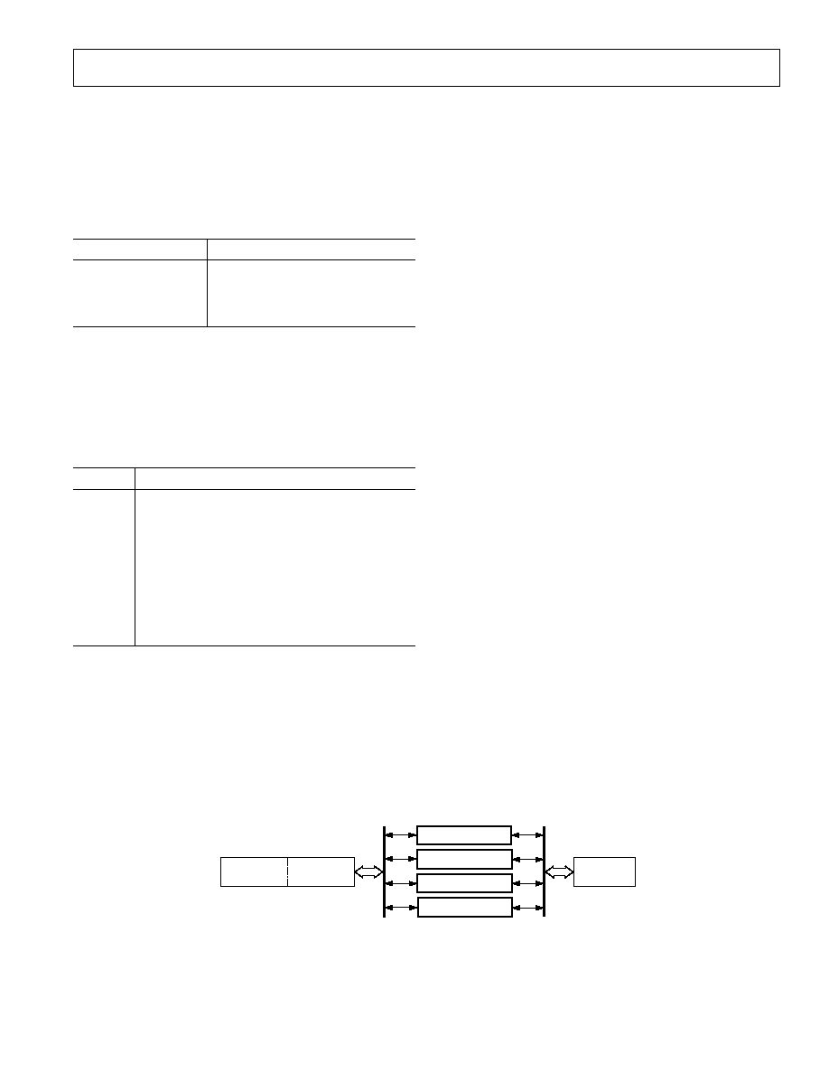
Serial Telco PCM TDM Data Stream Architecture
The serial Telco PCM TDM data stream architecture, shown in
Figure 5, is the most common architecture. In this architecture,
the data pump pool may have a local Telco interface that pro-
vides a serial TDM data stream of Telco PCM data to the DSP
through the DSP's Serial Port. Up to 24/32 DSPs can be con-
nected, through the Serial Port, to a 24/32 channel serial TDM
data stream.
NOTE: The Controller and Host can be configured in either a single machine, as shown in Figure 5, or two separate ones.
ADSP-21mod970
TELCO PCM
I/F
HOST
MEMORY I/F
DMA
PORT
SERIAL
PORT
CONTROLLER
ADSP-21mod970
ADSP-21mod970
ADSP-21mod970
Figure 5. Serial Telco PCM TDM Data Stream Architecture
REV. 0
8
C36362.57/99
PRINTED IN U.S.A.
ADSP-21mod970-510
COM
INTERFACE
AT
PARSER
CONTROL
SEQUENCER
ADSP-21mod970-510 HARDWARE
PRI / T1 BOARD
DATA
COMPRESSION
ERROR
CONTROL
DSP FIFO
INTERFACE
DSP CONTROL
INTERFACE
DSP DOWNLOAD
MANAGEMENT
PRIBOARD
CONFIGURATION
PRIBOARD CALL
MANAGEMENT
Figure 6. Development Platform Block Diagram
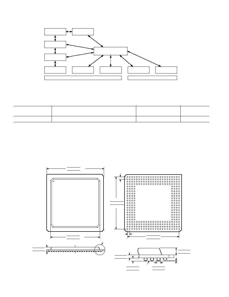
OUTLINE DIMENSIONS
Dimensions shown in inches and (mm).
ORDERING GUIDE
To receive a copy of the Digital Modem Software License Agreement, contact Analog Devices at (781) 461-3881.
Package
Part Number
Description
Processor Clock MHz
Description
ADSP-21mod970-510
312 MIPS DSP with Modem Software Unit License
26.0
304-Ball PBGA
RELATED DOCUMENTS
· ADSP-21mod970 Multiport Internet Gateway Processor Technical Data.
304-Plastic Ball Grid Array
(BP-304)
0.048 (1.22)
0.046 (1.17)
0.044 (1.12)
SEATING
PLANE
0.008 (0.20)
MAX
DETAIL A
0.035 (0.90)
0.030 (0.75)
0.024 (0.60)
BALL DIAMETER
0.024 (0.62)
0.022 (0.56)
0.020 (0.50)
0.028 (0.70)
0.024 (0.60)
0.020 (0.50)
DETAIL A
0.100 (2.54)
0.092 (2.33)
0.083 (2.12)
1.224 (31.10)
1.220 (31.00) SQ
1.217 (30.90)
1.051 (26.70)
1.037 (26.35) SQ
1.024 (26.00)
TOP VIEW
0.050 (1.27)
BSC
1.104 (28.04)
1.100 (27.94)
1.096 (27.84)
0.050 (1.27)
BSC
BOTTOM VIEW
A
B
C
D
E
F
G
H
J
K
L
M
N
P
R
T
U
V
W
Y
AA
AB
AC
23 22 21 20 19 18 17 16 15 14 13 12 11 10 9 8 7 6 5 4 3 2 1
1.104 (28.04)
1.100 (27.94)
1.096 (27.84)
NOTE
1. THE ACTUAL POSITION OF THE BALL GRID IS WITHIN 0.012 (0.30)
OF THE IDEAL POSITION RELATIVE TO THE PACKAGE EDGES.
2. THE ACTUAL POSITION OF EACH BALL IS WITHIN 0.004 (0.10) OF ITS
IDEAL POSITION RELATIVE TO THE BALL GRID.
3. CENTER FIGURES ARE TYPICAL UNLESS OTHERWISE NOTED.