 | ÐлекÑÑоннÑй компоненÑ: ADR121 | СкаÑаÑÑ:  PDF PDF  ZIP ZIP |
ADR121/ADR125/ADR127 Precision Micropower LDO Voltage References in TSOT Data Sheet (Rev. 0)

Precision, Micropower LDO Voltage
References in TSOT
ADR121/ADR125/ADR127
Rev. 0
Information furnished by Analog Devices is believed to be accurate and reliable. However, no
responsibility is assumed by Analog Devices for its use, nor for any infringements of patents or other
rights of third parties that may result from its use. Specifications subject to change without notice. No
license is granted by implication or otherwise under any patent or patent rights of Analog Devices.
Trademarks and registered trademarks are the property of their respective owners.
One Technology Way, P.O. Box 9106, Norwood, MA 02062-9106, U.S.A.
Tel: 781.329.4700
www.analog.com
Fax: 781.461.3113
©2006 Analog Devices, Inc. All rights reserved.
FEATURES
Initial accuracy
A grade: ±0.24%
B grade: ±0.12%
Maximum tempco
A grade: 25 ppm/°C
B grade: 9 ppm/°C
Low dropout: 300 mV for ADR121, ADR125
High output current: +5 mA/-2 mA
Low typical operating current: 85 A
Input range: 2.7 V to 18 V
Temperature range: -40°C to +125°C
Tiny TSOT (UJ-6) package
APPLICATIONS
Battery-powered instrumentation
Portable medical equipment
Data acquisition systems
Automotive
PIN CONFIGURATION
NC
1
1
GND
2
V
IN 3
NC
1
6
V
OUT
4
NC
1
1
MUST BE LEFT FLOATING
5
NC = NO CONNECT
ADR12x
TOP VIEW
(Not to Scale)
05
72
5-
0
01
Figure 1.
GENERAL DESCRIPTION
The ADR121/ADR125/ADR127 are a family of micropower,
high precision, series mode, band gap references with sink and
source capability. The parts feature high accuracy and low
power consumption in a tiny package. The ADR12x design
includes a patented temperature drift curvature correction
technique that minimizes the nonlinearities in the output
voltage vs. temperature characteristics.
The ADR12x is a low dropout voltage reference, requiring only
300 mV for ADR121/ADR125 and 1.45 V for ADR127 above
the nominal output voltage on the input to provide a stable
output voltage. This low dropout performance coupled with the
low 85 A operating current makes the ADR12x ideal for
battery-powered applications.
Available in an extended industrial temperature range of -40°C
to +125°C, the ADR12x is housed in the tiny TSOT (UJ-6)
package.

ADR121/ADR125/ADR127
Rev. 0 | Page 2 of 20
TABLE OF CONTENTS
Features .............................................................................................. 1
Applications....................................................................................... 1
Pin Configuration............................................................................. 1
General Description ......................................................................... 1
Revision History ............................................................................... 2
Specifications..................................................................................... 3
ADR121 Electrical Characteristics............................................. 3
ADR125 Electrical Characteristics............................................. 4
ADR127 Electrical Characteristics............................................. 5
Absolute Maximum Ratings............................................................ 6
Thermal Resistance ...................................................................... 6
ESD Caution.................................................................................. 6
Terminology .......................................................................................7
Typical Performance Characteristics ..............................................8
Theory of Operation ...................................................................... 16
Power Dissipation Considerations........................................... 16
Notes ............................................................................................ 16
Applications..................................................................................... 17
Basic Voltage Reference Connection ....................................... 17
Stacking Reference ICs for Arbitrary Outputs ....................... 17
Negative Precision Reference Without Precision Resistors.. 17
General-Purpose Current Source ............................................ 17
Outline Dimensions ....................................................................... 18
Ordering Guide .......................................................................... 18
REVISION HISTORY
6/06--Revision 0: Initial Version
ADR121/ADR125/ADR127
Rev. 0 | Page 3 of 20
SPECIFICATIONS
ADR121 ELECTRICAL CHARACTERISTICS
@ T
A
= 25°C, V
IN
= 2.8 V to 18 V, I
OUT
= 0 mA, unless otherwise noted.
Table 1.
Parameter Symbol
Conditions/Comments
Min
Typ
Max
Unit
OUTPUT VOLTAGE
V
O
@
25°C
B Grade
2.497
2.5
2.503
V
A Grade
2.494
2.5
2.506
V
INITIAL ACCURACY ERROR
V
OERR
@
25°C
B Grade
-0.12
+0.12
%
A Grade
-0.24
+0.24
%
TEMPERATURE COEFFICIENT
TCV
O
-40°C
<
T
A
< +125°C
B Grade
3
9
ppm/°C
A Grade
15
25
ppm/°C
DROPOUT (V
OUT
- V
IN
) V
DO
I
OUT
= 0 mA
300
mV
LOAD REGULATION
-40°C < T
A
< +125°C; V
IN
= 3.0 V,
0 mA < I
OUT
< 5 mA
80
300
ppm/mA
-40°C
<
T
A
< +125°C; V
IN
= 3.0 V,
-2 mA < I
OUT
< 0 mA
50
300
ppm/mA
LINE REGULATION
2.8 V to 18 V
I
OUT
= 0 mA
-50
+3
+50
ppm/V
PSRR
f = 1 Khz
-90
dB
RIPPLE REJECTION
V
OUT
/
V
IN
f = 60 Hz
60
dB
QUIESCENT CURRENT
I
Q
-40°C
<
T
A
< +125°C, no load
V
IN
= 18 V
95
125
A
V
IN
= 2.8 V
80
95
A
SHORT-CIRCUIT CURRENT TO GROUND
V
IN
= 2.8 V
18
mA
V
IN
= 18 V
40
mA
VOLTAGE NOISE
@ 25°C
f = 10 KHz
500
nV/Hz
0.1 Hz to 10 Hz
10
V p-p
TURN-ON SETTLING TIME
To 0.1%, C
L
= 0.2 F
100
s
LONG-TERM STABILITY
1000 hours @ 25°C
150
ppm/1000 hrs
OUTPUT VOLTAGE HYSTERESIS
See the Terminology section
300
ppm
ADR121/ADR125/ADR127
Rev. 0 | Page 4 of 20
ADR125 ELECTRICAL CHARACTERISTICS
@ T
A
= 25°C, V
IN
= 5.3 V to 18 V, I
OUT
= 0 mA, unless otherwise noted.
Table 2.
Parameter Symbol
Condition
Min
Typ
Max
Unit
OUTPUT VOLTAGE
V
O
@
25°C
B Grade
4.994
5.0
5.006
V
A Grade
2.497
4.988
5.0
5.012
V
INITIAL ACCURACY ERROR
V
OERR
@
25°C
B Grade
-0.12
+0.12
%
A Grade
-0.24
+0.24
%
TEMPERATURE COEFFICIENT
TCV
O
-40°C
<
T
A
< +125°C
B Grade
3
9
ppm/°C
A Grade
15
25
ppm/°C
DROPOUT (V
OUT
- V
IN
) V
DO
I
OUT
= 5 mA
300
mV
LOAD REGULATION
-40°C < T
A
< +125°C; V
IN
= 3.0 V,
0 mA < I
OUT
< 5 mA
35
200
ppm/mA
-40°C
<
T
A
< +125°C; V
IN
= 3.0 V,
-2 mA < I
OUT
< 0 mA
35
200
ppm/mA
LINE REGULATION
5.3 V < V
IN
< 18 V
I
OUT
= 0 mA
30
ppm/V
PSRR
f = 60 Hz
-90
dB
RIPPLE REJECTION
V
OUT
/
V
IN
f = 60 Hz
60
dB
QUIESCENT CURRENT
I
Q
-40°C
<
T
A
< +125°C, no load
V
IN
= 18 V
95
125
A
V
IN
= 3.0 V
80
95
A
SHORT-CIRCUIT CURRENT TO GROUND
V
IN
= 5.3 V
25
mA
V
IN
= 18 V
40
mA
VOLTAGE NOISE
@ 25°C
f = 10 Khz
900
nV/Hz
0.1 Hz to 10 Hz
20
V p-p
TURN-ON SETTLING TIME
To 0.1%, C
L
= 0.2 F
100
s
LONG-TERM STABILITY
1000 hours @ 25°C
150
ppm/1000 hrs
OUTPUT VOLTAGE HYSTERESIS
See the Terminology section
300
ppm
ADR121/ADR125/ADR127
Rev. 0 | Page 5 of 20
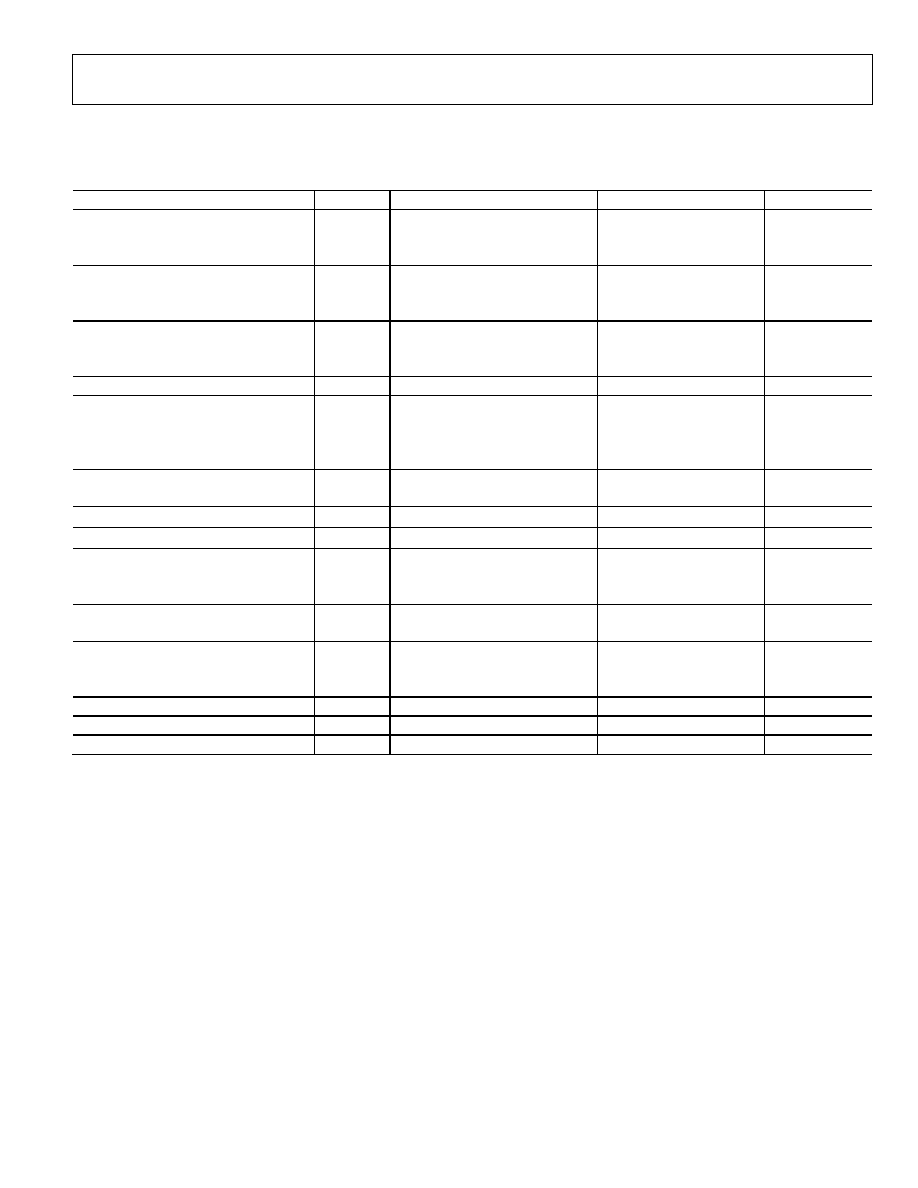
ADR127 ELECTRICAL CHARACTERISTICS
@ T
A
= 25°C, 2.7 V to 18 V, I
OUT
= 0 mA, unless otherwise noted.
Table 3.
Parameter Symbol
Condition
Min
Typ
Max
Unit
OUTPUT VOLTAGE
V
O
@
25°C
B Grade
1.2485
1.25
1.2515
V
A Grade
1.2470
1.25
1.2530
V
INITIAL ACCURACY ERROR
V
OERR
@
25°C
B Grade
-0.12
+0.12
%
A Grade
-0.24
+0.24
%
TEMPERATURE COEFFICIENT
TCV
O
-40°C
<
T
A
< +125°C
B Grade
3
9
ppm/°C
A Grade
15
25
ppm/°C
DROPOUT (V
OUT
- V
IN
) V
DO
I
OUT
= 0 mA
1.45
V
LOAD REGULATION
-40°C < T
A
< +125°C; V
IN
= 3.0 V,
0 mA < I
OUT
< 5 mA
85
400
ppm/mA
-40°C
<
T
A
< +125°C; V
IN
= 3.0 V,
-2 mA < I
OUT
< 0 mA
65
400
ppm/mA
LINE REGULATION
2.7 V to 18 V
I
OUT
= 0 mA
30
90
ppm/V
PSRR
F = 60 Hz
-90
dB
RIPPLE REJECTION
V
OUT
/
V
IN
f = 60 Hz
60
dB
QUIENSCENT CURRENT
I
Q
-40°C
<
T
A
< +125°C, no load
V
IN
= 18 V
95
125
A
V
IN
= 2.7 V
80
95
A
SHORT-CIRCUIT CURRENT TO GROUND
V
IN
= 2.7 V
V
IN
= 18 V
15
30
mA
mA
VOLTAGE NOISE
@ 25°C
Noise Density
f = 10 kHz
300
nV/Hz
0.1 Hz to 10 Hz
5
V p-p
TURN-ON SETTLING TIME
To 0.1%, C
L
= 0.2 F
80
s
LONG-TERM STABILITY
1000 hours @ 25°C
150
ppm/1000 hrs
OUTPUT VOLTAGE HYSTERESIS
See the Terminology section
300
ppm
ADR121/ADR125/ADR127
Rev. 0 | Page 6 of 20
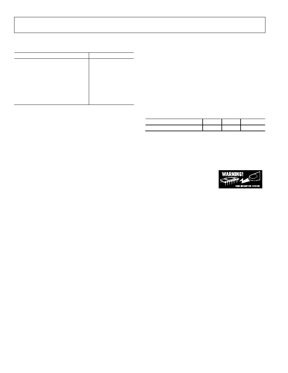
ABSOLUTE MAXIMUM RATINGS
Table 4.
Parameter Ratings
V
IN
to GND
20 V
Internal Power Dissipation
TSOT (UJ-6)
40 mW
Storage Temperature Range
-65°C to +150°C
Specified Temperature Range
-40°C to +125°C
Lead Temperature, Soldering
Vapor Phase (60 sec)
215°C
Infrared (15 sec)
220°C
Stresses above those listed under Absolute Maximum Ratings
may cause permanent damage to the device. This is a stress
rating only; functional operation of the device at these or any
other conditions above those indicated in the operational
section of this specification is not implied. Exposure to absolute
maximum rating conditions for extended periods may affect
device reliability.
THERMAL RESISTANCE
JA
is specified for the worst-case conditions, that is, a device
soldered in a circuit board for surface-mount packages.
Table 5. Thermal Resistance
Package Type
JA
JC
Unit
TSOT (UJ-6)
230
146
°C/W
ESD CAUTION
ESD (electrostatic discharge) sensitive device. Electrostatic charges as high as 4000 V readily accumulate on
the human body and test equipment and can discharge without detection. Although this product features
proprietary ESD protection circuitry, permanent damage may occur on devices subjected to high energy
electrostatic discharges. Therefore, proper ESD precautions are recommended to avoid performance
degradation or loss of functionality.

ADR121/ADR125/ADR127
Rev. 0 | Page 7 of 20
TERMINOLOGY
Temperature Coefficient
The change of output voltage with respect to operating
temperature change normalized by the output voltage at 25°C.
This parameter is expressed in ppm/°C and can be determined
by
[
]
( )
( )
(
)
(
)
6
1
2
1
2
10
C
25
C
ppm/
×
-
×
°
-
=
°
T
T
V
T
V
T
V
TCV
O
O
O
O
where:
V
O
(25°C) = V
O
at 25°C.
V
O
(T
1
) = V
O
at Temperature 1.
V
O
(T
2
) = V
O
at Temperature 2.
Line Regulation
The change in the output due to a specified change in input
voltage. This parameter accounts for the effects of self-heating.
Line regulation is expressed in either percent per volt, parts-
per-million per volt, or microvolts per voltage changes in input
voltage.
Load Regulation
The change in output voltage due to a specified change in load
current. This parameter accounts for the effects of self-heating.
Load regulation is expressed in either microvolts per milliam-
pere, parts-per-million per milliampere, or ohms of dc output
resistance.
Long-Term Stability
Typical shift of output voltage at 25°C on a sample of parts
subjected to a test of 1000 hours at 25°C.
( )
( )
[
]
( )
( )
( )
6
1
1
10
ppm
×
-
=
-
=
O
O
O
O
O
O
O
O
O
O
t
V
t
V
t
V
V
t
V
t
V
V
where:
V
O
(t
0
) = V
O
at 25°C at Time 0.
V
O
(t
1
) = V
O
at 25°C after 1000 hours operating at 25°C.
Thermal Hysteresis
The change of output voltage after the device is cycled through
temperatures from +25°C to -40°C to +125°C and back to
+25°C. This is a typical value from a sample of parts put
through such a cycle.
where:
V
O
(25°C) = V
O
at 25°C.
V
OTC
= V
O
at 25°C after temperature cycle at +25°C to -40°C to
+125°C and back to +25°C.
ADR121/ADR125/ADR127
Rev. 0 | Page 8 of 20
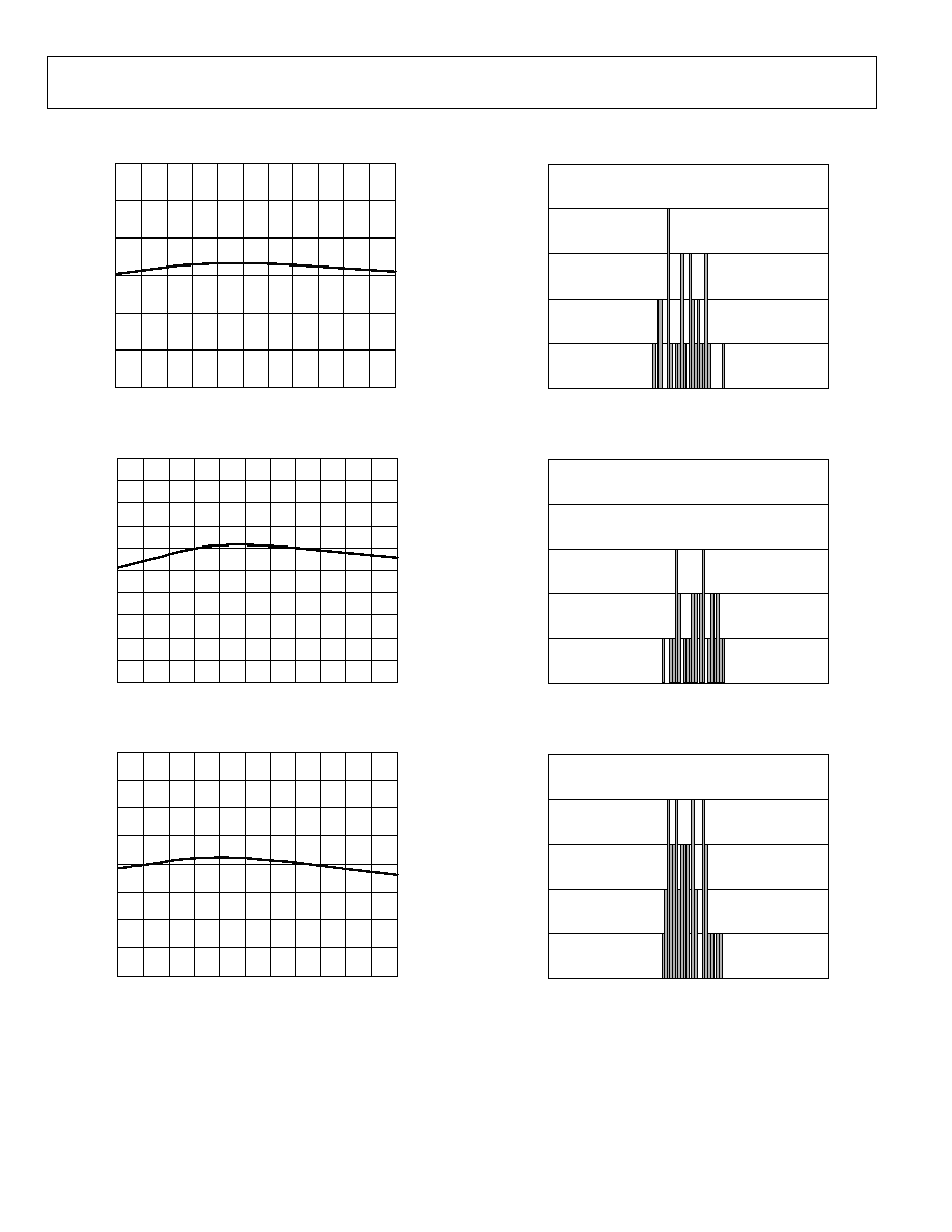
TYPICAL PERFORMANCE CHARACTERISTICS
1.256
1.244
40
125
TEMPERATURE (°C)
V
OU
T
(V
)
05
72
5-
0
06
1.246
1.248
1.250
1.252
1.254
25 10
5
20
35
50
65
80
95
110
Figure 2. ADR127 V
OUT
vs. Temperature
2.510
2.490
40
125
TEMPERATURE (°C)
V
OU
T
(V
)
0
572
5-
0
07
2.492
2.494
2.496
2.498
2.500
2.502
2.504
2.506
2.508
25 10
5
20
35
50
65
80
95
110
Figure 3. ADR121 V
OUT
vs. Temperature
5.020
4.980
40
125
TEMPERATURE (°C)
V
OU
T
(V
)
0
572
5-
0
08
25 10
5
20
35
50
65
80
95
110
4.985
4.990
4.995
5.000
5.005
5.010
5.015
Figure 4. ADR125 V
OUT
vs. Temperature
5
0
50
50
TEMPERATURE COEFFICIENT (ppm/°C)
N
U
M
B
ER
O
F
PA
R
T
S
0
572
5-
0
09
1
2
3
4
40
30
20
10
0
10
20
30
40
Figure 5. ADR127 Temperature Coefficient
5
0
50
50
TEMPERATURE COEFFICIENT (ppm/°C)
NUM
BE
R O
F
P
ART
S
0
572
5-
0
10
1
2
3
4
40
30
20
10
0
10
20
30
40
Figure 6. ADR125 Temperature Coefficient
5
0
50
50
TEMPERATURE COEFFICIENT (ppm/°C)
NUM
BE
R O
F
P
A
RT
S
0
572
5-
0
11
1
2
3
4
40
30
20
10
0
10
20
30
40
Figure 7. ADR121 Temperature Coefficient
ADR121/ADR125/ADR127
Rev. 0 | Page 9 of 20
3.0
2.0
2
1
0
1
2
3
4
5
LOAD CURRENT (mA)
V
I
N_M
I
N (
V
)
0
57
25
-
0
12
2.2
2.4
2.6
2.8
+125°C
40°C
+25°C
Figure 8. ADR127 Minimum Input Voltage vs. Load Current
3.5
2.5
2
1
0
1
2
3
4
5
LOAD CURRENT (mA)
V
I
N_M
I
N (
V
)
05
72
5-
01
3
2.6
2.7
2.8
2.9
3.0
3.1
3.2
3.3
3.4
40°C
+25°C
+125°C
Figure 9. ADR121 Minimum Input Voltage vs. Load Current
6.2
5.0
2
1
0
1
2
3
4
5
LOAD CURRENT (mA)
V
I
N_M
I
N (
V
)
05
72
5-
01
4
+25°C
+125°C
5.2
5.4
5.6
5.8
6.0
40°C
Figure 10. ADR125 Minimum Input Voltage vs. Load Current
120
0
2
1
INPUT VOLTAGE (V)
S
U
P
P
L
Y
CUR
RE
NT
(
µ
A)
8
0
57
25
-
0
15
20
40
60
80
100
3
4
5
6
7
8
9 10 11 12 13 14 15 16 17
+25°C
40°C
+125°C
Figure 11. ADR127 Supply Current vs. Input Voltage
120
0
2
1
INPUT VOLTAGE (V)
S
U
P
P
L
Y
CUR
RE
NT
(
µ
A)
8
05
72
5-
0
16
20
40
60
80
100
3
4
5
6
7
8
9 10 11 12 13 14 15 16 17
+25°C
40°C
+125°C
Figure 12. ADR121 Supply Current vs. Input Voltage
120
0
5
1
INPUT VOLTAGE (V)
SU
PPL
Y C
U
R
R
EN
T
(
µ
A
)
8
0
57
25
-
0
17
20
40
60
80
100
6
7
8
9
10
11
12
13
14
15
16
17
+25°C
40°C
+125°C
Figure 13. ADR125 Supply Current vs. Input Voltage
ADR121/ADR125/ADR127
Rev. 0 | Page 10 of 20
6
0
2
5
LOAD CURRENT (mA)
S
UP
P
L
Y
CURRE
NT
(
m
A
)
05
72
5-
01
8
5
4
3
2
1
1
0
1
2
3
4
--
+125°C
-- +25°C
--
40°C
Figure 14. ADR127 Supply Current vs. Load Current
6
0
2
5
LOAD CURRENT (mA)
S
UP
P
L
Y
CURR
E
NT
(
m
A)
05
72
5-
01
9
5
4
3
2
1
1
0
1
2
3
4
--
+125°C
-- +25°C
--
40°C
Figure 15. ADR121 Supply Current vs. Load Current
6
0
2
5
LOAD CURRENT (mA)
S
UP
P
L
Y
CURRE
NT
(
m
A)
05
72
5-
0
20
5
4
3
2
1
1
0
1
2
3
4
--
+125°C
-- +25°C
--
40°C
Figure 16. ADR125 Supply Current vs. Load Current
0
50
40
125
TEMPERATURE (°C)
L
I
NE
RE
G
U
L
AT
I
O
N
(
p
p
m
/
V
)
05
72
5-
0
21
40
30
20
10
-25
-10
5
20
35
50
65
80
95
110
V
IN
= 2.7V TO 18V
Figure 17. ADR127 Line Regulation vs. Temperature
3
3
40
125
TEMPERATURE (°C)
L
I
NE
RE
G
U
L
AT
I
O
N
(
p
p
m
/
V
)
05
72
5-
0
22
2
1
0
2
25 10
5
20
35
50
65
80
95
110
1
V
IN
= 2.8V TO 18V
Figure 18. ADR121 Line Regulation vs. Temperature
6
6
40
125
TEMPERATURE (°C)
L
I
NE
RE
G
UL
AT
I
O
N (
p
p
m
/
V
)
05
72
5-
0
23
4
2
0
4
25 10
5
20
35
50
65
80
95
110
2
V
IN
= 5.3V TO 18V
Figure 19. ADR125 Line Regulation vs. Temperature
ADR121/ADR125/ADR127
Rev. 0 | Page 11 of 20
200
200
40
125
TEMPERATURE (°C)
L
O
AD RE
G
UL
AT
I
O
N (
p
p
m
/
m
A)
05
72
5-
0
24
25 10
5
20
35
50
65
80
95
110
150
100
50
0
50
100
150
2mA SINKING, V
IN
= 3V
5mA SOURCING, V
IN
= 3V
Figure 20. ADR127 Load Regulation vs. Temperature
100
100
40
125
TEMPERATURE (°C)
L
O
AD RE
G
UL
AT
I
O
N (
p
p
m
/
m
A)
05
72
5-
0
25
25 10
5
20
35
50
65
80
95
110
5mA SOURCING, V
IN
= 5V
80
60
40
20
0
20
40
60
80
2mA SINKING, V
IN
= 5V
Figure 21. ADR121 Load Regulation vs. Temperature
50
50
40
125
TEMPERATURE (°C)
LO
A
D
R
E
G
U
LA
TI
O
N
(
pp
m
/
m
A
)
05
72
5-
0
26
25 10
5
20
35
50
65
80
95
110
40
30
20
10
0
10
20
30
40
2mA SINKING, V
IN
= 6V
5mA SOURCING, V
IN
= 6V
Figure 22. ADR125 Load Regulation vs. Temperature
057
25
-
02
7
1
C
IN
= C
OUT
= 0.1µF
2µV/DIV
TIME (1s/DIV)
CH1 p-p
5.76µV
CH1 rms
0.862µV
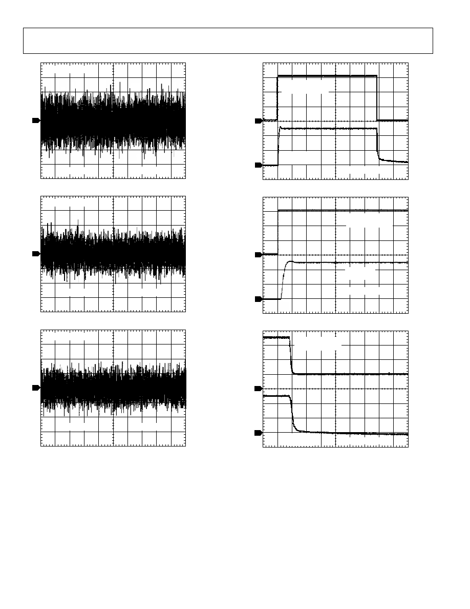
Figure 23. ADR127 0.1 Hz to 10 Hz Noise
05
72
5-
02
8
1
C
IN
= C
OUT
= 0.1µF
5µV/DIV
TIME (1s/DIV)
CH1 p-p
10.8µV
CH1 rms
1.75µV
Figure 24. ADR121 0.1 Hz to 10 Hz Noise
0
5725
-
0
29
1
C
IN
= C
OUT
= 0.1µF
10µV/DIV
TIME (1s/DIV)
CH1 p-p
20.6µV
CH1 rms
3.34µV
Figure 25. ADR125 0.1 Hz to 10 Hz Noise
ADR121/ADR125/ADR127
Rev. 0 | Page 12 of 20
0
5725
-
0
30
1
C
IN
= C
OUT
= 0.1µF
50µV/DIV
TIME (1s/DIV)
CH1 p-p
287µV
CH1 rms
38.8µV
Figure 26. ADR127 10 Hz to 10 KHz Noise
0
5725
-
0
31
1
C
IN
= C
OUT
= 0.1µF
100µV/DIV
TIME (1s/DIV)
CH1 p-p
450µV
CH1 rms
58.1µV
Figure 27. ADR121 10 Hz to 10 KHz Noise
05
72
5
-
03
2
1
C
IN
= C
OUT
= 0.1µF
200µV/DIV
TIME (1s/DIV)
CH1 p-p
788µV
CH1 rms
115µV
Figure 28. ADR125 10 Hz to 10 KHz Noise
05
72
5-
03
3
1
2
V
IN
1V/DIV
C
IN
= C
OUT
= 0.1µF
V
OUT
500mV/DIV
TIME (200µs/DIV)
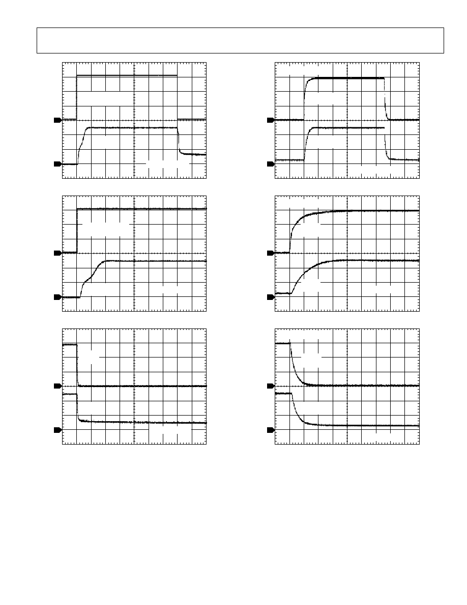
Figure 29. ADR127 Turn-On Response
05
72
5-
0
3
4
1
2
V
IN
1V/DIV
C
IN
= C
OUT
= 0.1µF
V
OUT
500mV/DIV
TIME (40µs/DIV)
Figure 30. ADR127 Turn-On Response
05
72
5-
03
5
1
2
V
IN
1V/DIV
C
IN
= C
OUT
= 0.1µF
V
OUT
500mV/DIV
TIME (100µs/DIV)
Figure 31. ADR127 Turn-Off Response
ADR121/ADR125/ADR127
Rev. 0 | Page 13 of 20
05
72
5-
03
6
1
2
V
IN
1V/DIV
C
IN
= C
OUT
= 0.1µF
V
OUT
1V/DIV
TIME (100µs/DIV)
Figure 32. ADR121 Turn-On Response
05
72
5-
0
3
7
1
2
V
IN
1V/DIV
C
IN
= C
OUT
= 0.1µF
V
OUT
1V/DIV
TIME (40µs/DIV)
Figure 33. ADR121 Turn-On Response
05
72
5-
0
3
8
1
2
V
IN
1V/DIV
V
OUT
1V/DIV
TIME (200µs/DIV)
Figure 34. ADR121 Turn-Off Response
05
72
5-
03
9
1
2
V
IN
2V/DIV
V
OUT
2V/DIV
TIME (100µs/DIV)
C
IN
= C
OUT
= 0.1µF
Figure 35. ADR125 Turn-On Response
05
72
5-
0
4
0
1
2
V
IN
2V/DIV
V
OUT
2V/DIV
TIME (20µs/DIV)
C
IN
= C
OUT
= 0.1µF
Figure 36. ADR125 Turn-On Response
05
72
5-
0
4
1
1
2
V
IN
2V/DIV
V
OUT
2V/DIV
TIME (20µs/DIV)
C
IN
= C
OUT
= 0.1µF
Figure 37. ADR125 Turn-Off Response
ADR121/ADR125/ADR127
Rev. 0 | Page 14 of 20
05
72
5-
04
2
1
2
V
IN
1V/DIV
LINE INTERRUPTION
V
OUT
500mV/DIV
TIME (200µs/DIV)
C
IN
= C
OUT
= 0.1µF
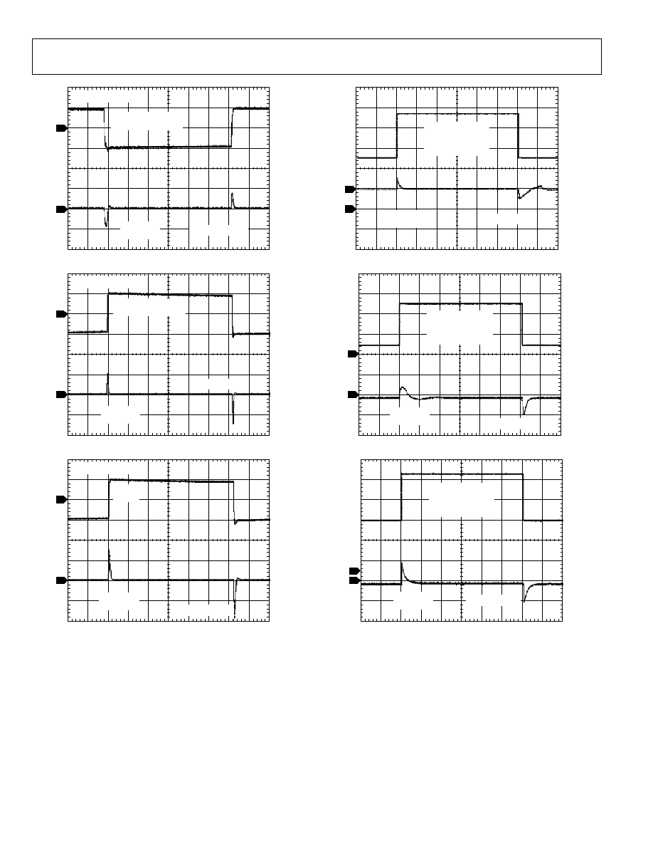
Figure 38. ADR127 Line Transient Response
05
72
5-
0
4
3
1
2
V
OUT
500mV/DIV
TIME (400µs/DIV)
LINE INTERRUPTION
1V/DIV
C
IN
= C
OUT
= 0.1µF
Figure 39. ADR121 Line Transient Response
05
72
5-
0
4
4
1
2
V
OUT
500mV/DIV
TIME (400µs/DIV)
V
IN
1V/DIV
C
IN
= C
OUT
= 0.1µF
Figure 40. ADR125 Line Transient Response
05
72
5-
04
5
2
1
V
OUT
20mV/DIV
TIME (40µs/DIV)
2.50V
1.25V
V
IN
500mV/DIV
C
IN
= C
OUT
= 0.1µF
625 LOAD
2mA SINKING
Figure 41. ADR127 Load Transient Response (Sinking)
05
72
5-
0
4
6
1
2
V
OUT
100mV/DIV
TIME (40µs/DIV)
1.25V
0V
V
IN
500mV/DIV
C
IN
= C
OUT
= 0.1µF
250 LOAD
5mA SOURCING
Figure 42. ADR127 Load Transient Response (Sourcing)
05
72
5-
0
4
7
1
2
V
OUT
10mV/DIV
TIME (40µs/DIV)
5V
2.5V
V
IN
1V/DIV
C
IN
= C
OUT
= 0.1µF
1250 LOAD
2mA SINKING
Figure 43. ADR121 Load Transient Response (Sinking)
ADR121/ADR125/ADR127
Rev. 0 | Page 15 of 20
05
72
5-
04
8
1
2
V
OUT
100mV/DIV
TIME (40µs/DIV)
2.5V
0V
V
IN
1V/DIV
C
IN
= C
OUT
= 0.1µF
500 LOAD
5mA SOURCING
Figure 44. ADR121 Load Transient Response (Sourcing)
05
72
5-
04
9
1
2
V
OUT
20mV/DIV
TIME (40µs/DIV)
10V
5V
V
IN
2V/DIV
C
IN
= C
OUT
= 0.1µF
2.5k LOAD
2mA SINKING
Figure 45. ADR125 Load Transient Response (Sinking)
05
72
5-
05
0
1
2
V
OUT
100mV/DIV
TIME (40µs/DIV)
5V
0V
V
IN
2V/DIV
C
IN
= C
OUT
= 0.1µF
1k LOAD
5mA SOURCING
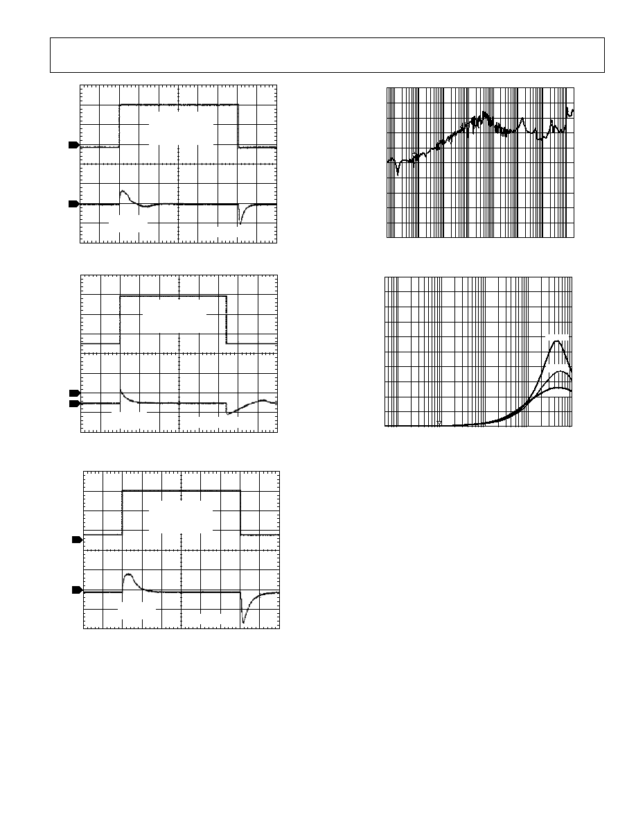
Figure 46. ADR125 Load Transient Response (Sourcing)
0
20
40
60
80
100
120
140
160
180
200
10
100M
(dB
)
05
72
5-
0
51
100
1k
10k
100k
1M
10M
1
Figure 47. ADR121/ADR125/ADR127 PSRR
10
O
UT
P
UT
I
M
P
E
DAN
CE
(
)
0
57
25
-
05
4
100
FREQUENCY (Hz)
1k
10k
100k
1
ADR121
ADR125
ADR127
50
45
40
35
30
25
20
15
10
5
0
Figure 48. ADR121/ADR125/ADR127 Output Impedance vs. Frequency

ADR121/ADR125/ADR127
Rev. 0 | Page 16 of 20
THEORY OF OPERATION
The ADR12x band gap references are the high performance
solution for low supply voltage and low power applications. The
uniqueness of these products lies in their architecture.
POWER DISSIPATION CONSIDERATIONS
The ADR12x family is capable of delivering load currents to
5 mA with an input range from 3.0 V to 18 V. When this device
is used in applications with large input voltages, care must be
taken to avoid exceeding the specified maximum power
dissipation or junction temperature, because this could result in
premature device failure.
Use the following formula to calculate a device's maximum
junction temperature or dissipation:
JA
A
J
D
T
T
P
-
=
where:
T
J
is the junction temperature.
T
A
is the ambient temperature.
P
D
is the device power dissipation.
JA
is the device package thermal resistance.
NOTES
Input Capacitor
Input capacitors are not required on the ADR12x. There is no
limit for the value of the capacitor used on the input, but a 1 F
to 10 F capacitor on the input improved transient response in
the applications where there is a sudden supply change. An
additional 0.1 F capacitor in parallel also helps reduce noise
from the supply.
Output Capacitor
The ADR12x requires a small 0.1 F capacitor for stability.
Additional 0.1 F to 10 F capacitance in parallel can improve
load transient response. This acts as a source of stored energy
for a sudden increase in load current. The only parameter
affected with the additional capacitance is turn-on time.
ADR121/ADR125/ADR127
Rev. 0 | Page 17 of 20
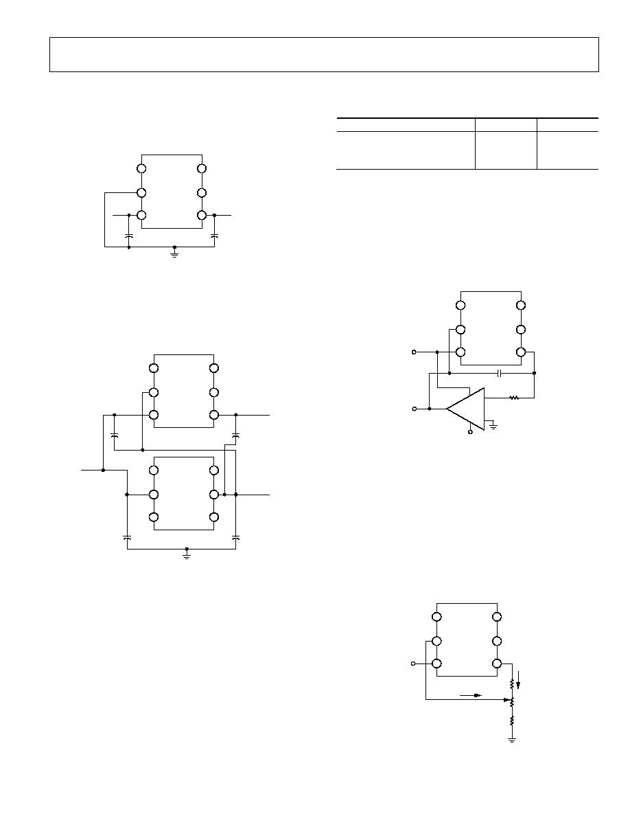
APPLICATIONS
BASIC VOLTAGE REFERENCE CONNECTION
The circuit in Figure 4 illustrates the basic configuration for the
ADR12x family voltage reference.
NC
V
OUT
NC
ADR12x
1
2
3
6
5
4
NC
GND
V
IN
0.1µF
0.1µF
OUTPUT
INPUT
+
+
05
72
5-
00
2
Figure 49. Basic Configuration for the ADR12x Family
STACKING REFERENCE ICs FOR ARBITRARY
OUTPUTS
Some applications may require two reference voltage sources
that are a combined sum of the standard outputs. Figure 50
shows how this stacked output reference can be implemented.
NC
V
OUT
NC
ADR12x
1
2
3
6
5
4
NC
GND
V
IN
0.1µF
0.1µF
OUTPUT1
+
+
NC
V
OUT
NC
ADR12x
1
2
3
6
5
4
NC
GND
V
IN
0.1µF
0.1µF
OUTPUT2
INPUT
+
+
05
72
5-
0
03
Figure 50. Stacking References with ADR12x
Two reference ICs are used and fed from an unregulated input,
V
IN
. The outputs of the individual ICs are connected in series,
which provide two output voltages, V
OUT1
and V
OUT2
. V
OUT1
is the
terminal voltage of U1, while V
OUT2
is the sum of this voltage
and the terminal of U2. U1 and U2 are chosen for the two
voltages that supply the required outputs (see Table 6). For
example, if U1 and U2 are ADR127 and V
IN
3.95 V, V
OUT1
is
1.25 V and V
OUT2
is 2.5 V.
Table 6. Required Outputs
U1/U2 V
OUT2
V
OUT1
ADR127/ADR121
1.25 V
3.75 V
ADR127/ADR125
1.25 V
6.25 V
ADR121/ADR125
2.5 V
7.5 V
NEGATIVE PRECISION REFERENCE WITHOUT
PRECISION RESISTORS
A negative reference is easily generated by adding an op amp,
A1, and is configured as shown in Figure 51. V
OUT1
is at virtual
ground and, therefore, the negative reference can be taken
directly from the output of the op amp. The op amp must be
dual-supply, low offset, and rail-to-rail if the negative supply
voltage is close to the reference output.
NC
V
OUT
NC
ADR127
AD8603
1
2
3
6
5
4
NC
GND
V+
V
3
2
+
V
IN
05
72
5-
0
55
0.1µF
+V
DD
V
REF
1k
V
DD
Figure 51. Negative Reference
GENERAL-PURPOSE CURRENT SOURCE
In low power applications, the need can arise for a precision
current source that can operate on low supply voltages. The
ADR12x can be configured as a precision current source (see
Figure 52). The circuit configuration shown is a floating current
source with a grounded load. The reference's output voltage is
bootstrapped across R
SET
, which sets the output current into the
load. With this configuration, circuit precision is maintained for
load currents ranging from the reference's supply current,
typically 85 A, to approximately 5 mA.
NC
V
OUT
NC
R1
ADR12x
1
2
3
6
5
4
NC
GND
V
IN
I
SY
+V
DD
RL
P1
I
SET
05
72
5-
0
05
Figure 52. ADR12x Trim Configuration
ADR121/ADR125/ADR127
Rev. 0 | Page 18 of 20
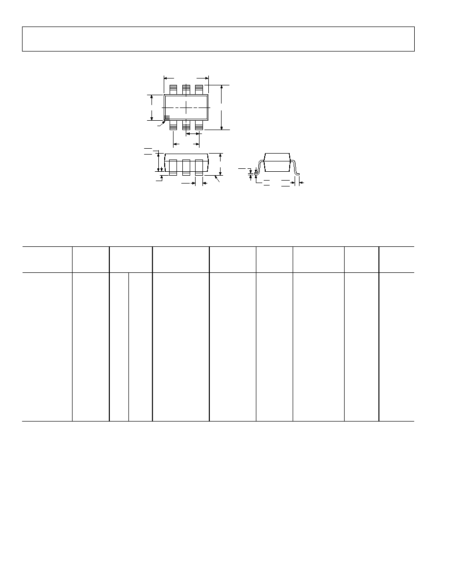
OUTLINE DIMENSIONS
1
3
4
5
2
6
2.90 BSC
1.60 BSC
2.80 BSC
1.90
BSC
0.95 BSC
0.20
0.08
8°
4°
0°
0.50
0.30
0.10 MAX
*0.90
0.87
0.84
SEATING
PLANE
*1.00 MAX
0.60
0.45
0.30
PIN 1
INDICATOR
*COMPLIANT TO JEDEC STANDARDS MO-193-AA WITH
THE EXCEPTION OF PACKAGE HEIGHT AND THICKNESS.
Figure 53. 6-Lead Thin Small Outline Transistor Package [TSOT]
(UJ-6)
Dimensions shown in millimeters
ORDERING GUIDE
Model
Output
Voltage
(V
O
)
Initial
Accuracy
(mV/%)
Temperature
Coefficient
(ppm/°C)
Package
Description
Package
Option
Temperature
Range (°C)
Ordering
Quantity
Branding
ADR121AUJZ-
REEL7
1
2.5 2.5
0.24
25
6-Lead
TSOT
UJ-6
-40°C to
+125°C
3000 R0N
ADR121AUJZ-
R2
1
2.5 2.5
0.24
25
6-Lead
TSOT
UJ-6
-40°C to
+125°C
250 R0N
ADR121BUJZ-
REEL7
1
2.5 2.5
0.12
9
6-Lead
TSOT
UJ-6
-40°C to
+125°C
3000 R0P
ADR125AUJZ-
REEL7
1
5.0 5.0
0.24
25
6-Lead
TSOT
UJ-6
-40°C to
+125°C
3000 R0Q
ADR125AUJZ-
R2
1
5.0 5.0
0.24
25
6-Lead
TSOT
UJ-6
-40°C to
+125°C
250 R0Q
ADR125BUJZ-
REEL7
1
5.0 5.0
0.12
9
6-Lead
TSOT
UJ-6
-40°C to
+125°C
3000 R0R
ADR127AUJZ-
REEL7
1
1.25 3
0.24
25
6-Lead
TSOT
UJ-6 -40°C to
+125°C
3000 R0S
ADR127AUJZ-
R2
1
1.25 3
0.24
25
6-Lead
TSOT
UJ-6 -40°C to
+125°C
250 R0S
ADR127BUJZ-
REEL7
1
1.25 1.5
0.12
9
6-Lead
TSOT
UJ-6 -40°C to
+125°C
3000 R0T
1
Z = Pb-free part.

ADR121/ADR125/ADR127
Rev. 0 | Page 19 of 20
NOTES

ADR121/ADR125/ADR127
Rev. 0 | Page 20 of 20
NOTES
©2006 Analog Devices, Inc. All rights reserved. Trademarks and
registered trademarks are the property of their respective owners.
D05725-0-6/06(0)
Document Outline
- þÿ
- þÿ
- PIN CONFIGURATION
- þÿ
- þÿ
- þÿ
- þÿ
- þÿ
- ADR125 ELECTRICAL CHARACTERISTICS
- ADR127 ELECTRICAL CHARACTERISTICS
- þÿ
- þÿ
- þÿ
- þÿ
- þÿ
- þÿ