 | ÐлекÑÑоннÑй компоненÑ: ADP3607 | СкаÑаÑÑ:  PDF PDF  ZIP ZIP |
Äîêóìåíòàöèÿ è îïèñàíèÿ www.docs.chipfind.ru
REV. 0
Information furnished by Analog Devices is believed to be accurate and
reliable. However, no responsibility is assumed by Analog Devices for its
use, nor for any infringements of patents or other rights of third parties
which may result from its use. No license is granted by implication or
otherwise under any patent or patent rights of Analog Devices.
a
ADP3607
One Technology Way, P.O. Box 9106, Norwood, MA 02062-9106, U.S.A.
Tel: 781/329-4700
World Wide Web Site: http://www.analog.com
Fax: 781/326-8703
© Analog Devices, Inc., 1999
50 mA Switched Capacitor
Voltage Boost with Regulated Output
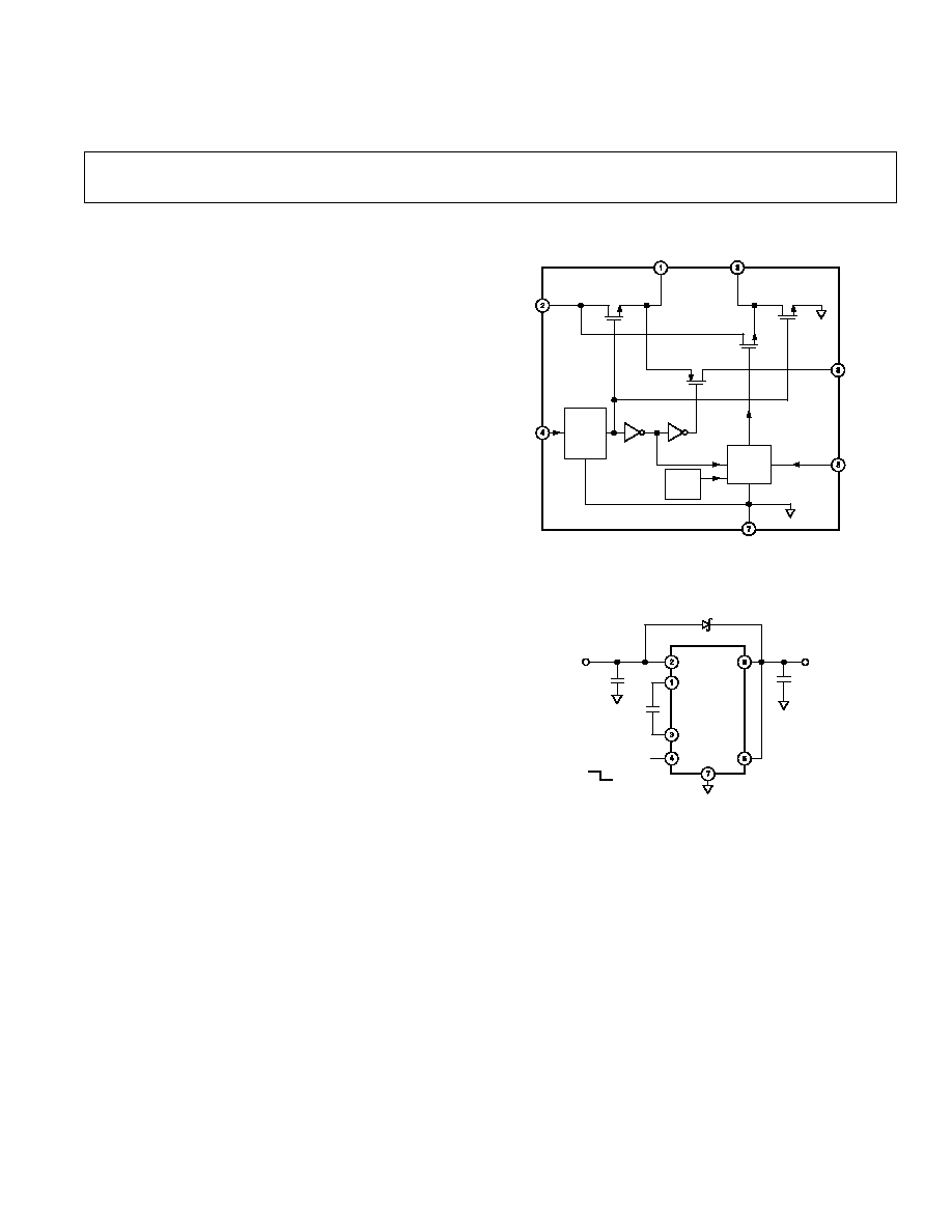
FUNCTIONAL BLOCK DIAGRAM
OSC
CLOCK
GEN
1.5 V
V
REF
S1
C
P
GND
C
P
+
V
OUT
S3
FB
V
SENSE
S2
S4
SD
V
IN
+
V
OUT
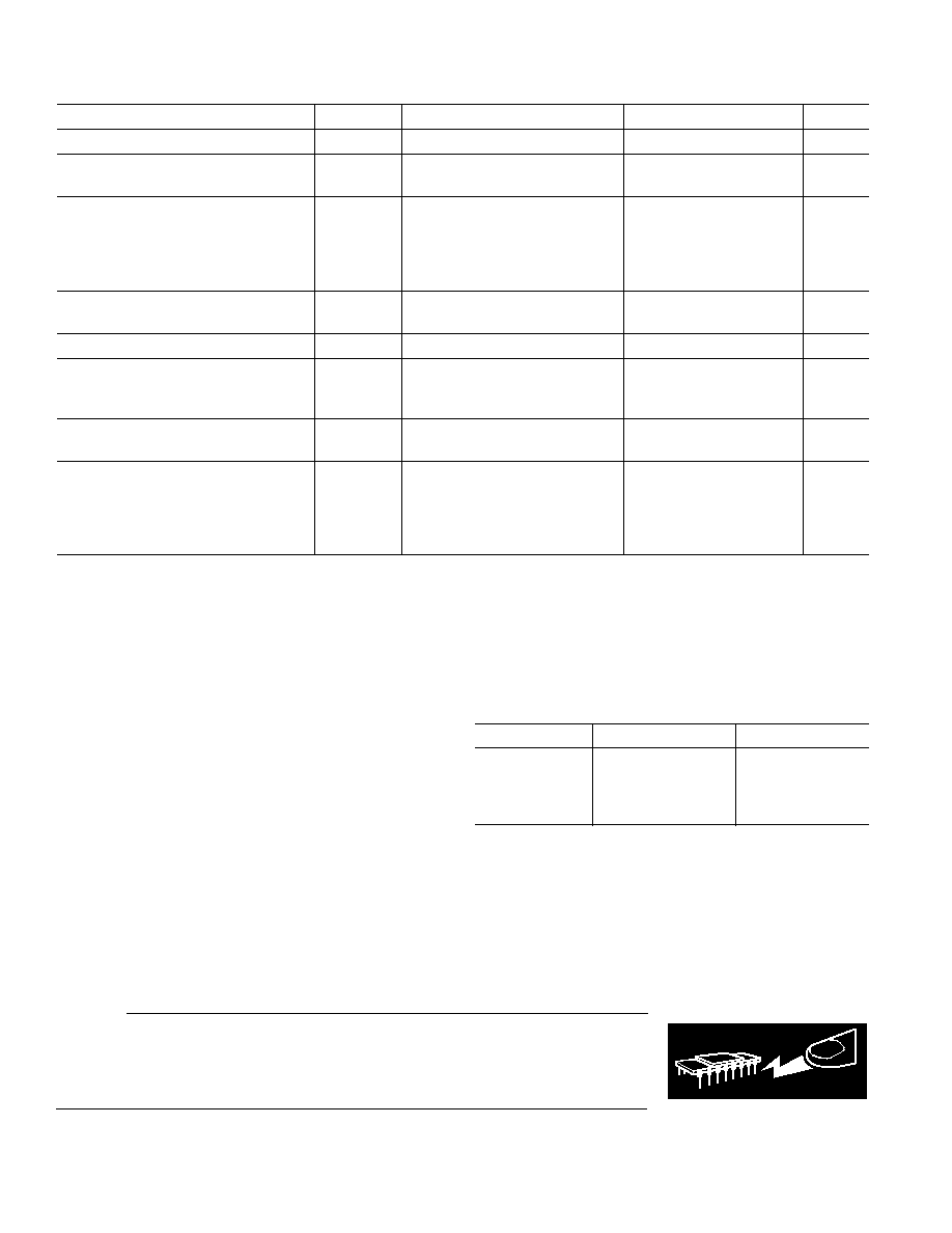
5.0V
V
IN
3.3V
*C
O
4.7 F
+
*C
IN
4.7 F
+
ADP3607-5
*C
P
4.7 F
OFF
ON
0
V
SENSE
V
IN
C
P
+
C
P
SD
V
OUT
*FOR BEST PERFORMANCE, 10 F IS RECOMMENDED
C
P
: SPRAGUE, 293D475X0010B2W
C
IN
, C
O
: TOKIN, 1E475ZY5UC205F
GND
D1
SD103
Figure 1. Typical Application Circuit
FEATURES
Fully Regulated Output Voltage (5 V and Adjustable)
Input Voltage Range From 3 V to 5 V
50 mA Output Current
Output Accuracy: 5%
High Switching Frequency: 250 kHz
SO-8 and TSSOP-8 Packages
40 C to +85 C Ambient Temperature Range
A P P L I C A T I O N S
Computer Peripherals and Add-On Cards
Portable Instruments
Battery Powered Devices
Pagers and Radio Control Receivers
Disk Drives
Mobile Phones
GENERAL DESCRIPTION
The ADP3607 is a 50 mA regulated output switched capacitor
voltage doubler. It provides a regulated output voltage with
minimum voltage loss and requires a minimum number of ex-
ternal components. In addition, the ADP3607 does not require
the use of an inductor.
The internal oscillator of the ADP3607 runs at 500 kHz nomi-
nal frequency, which produces an output switching frequency of
250 kHz. This allows for the use of smaller charge pump and
filter capacitors.
The ADP3607 provides an accuracy of
±
5% with a typical shut-
down current of 150
µ
A. It can also operate from a single posi-
tive input voltage as low as 3 V. The ADP3607 is offered with
the regulation fixed at 5 V, or adjustable via external resistors
over a 3 V to 9 V range.
REV. 0
2
ADP3607SPECIFICATIONS
1, 2, 3
Parameter
Symbol
Condition
Min
Typ
Max
Units
OPERATING SUPPLY RANGE
V
S
3.0
3.3
5
V
SUPPLY CURRENT
I
S
40
°
C < T
A
< +85
°
C
3.5
6
mA
Shutdown Mode
V
SD
= V
IN
, 40
°
C < T
A
< +85
°
C
150
200
µ
A
OUTPUT VOLTAGE
4
V
O
I
O
= 25 mA
4.85
5
5.15
V
V
O
I
O
= 10 mA to 50 mA
4.75
5
5.25
V
40
°
C
T
A
+85
°
C
3.0 V
V
S
3.6 V
LOAD REGULATION
V
O
/I
O
I
O
= 10 mA25 mA
0.3
mV/mA
I
O
= 10 mA50 mA
0.25
mV/mA
OUTPUT RESISTANCE (Open Loop)
R
O
11
OUTPUT RIPPLE VOLTAGE
V
RIPPLE
C
IN
= C
O
= 4.7
µ
F
I
LOAD
= 25 mA
16
mV
I
LOAD
= 50 mA
31
mV
SWITCHING FREQUENCY
f
S
V
IN
= 3.3 V
40
°
C < T
A
< +85
°
C
212
250
288
kHz
SHUTDOWN
Logic Input High
V
IH
2.4
V
Input Current
I
IH
1
µ
A
Logic Input Low
V
IL
0.4
V
Input Current
I
IL
1
µ
A
NOTES
1
Capacitors C
IN
, C
O
and C
P
in the test circuit are 4.7
µ
F with 0.1
ESR. Capacitors with higher ESR may reduce output voltage and efficiency.
2
See Figure 1 conditions.
3
All limits at temperature extremes are guaranteed via correlation using standard Statistical Quality Control (SQC) methods.
4
For the adjustable version, a 1% resistor should be used to maintain output voltage tolerance. For both device types, tolerances can be improved by >1% using larger
value and lower ESR capacitors for C
O
and C
P
.
Specifications subject to change without notice.
(V
IN
= 3.3 V @ T
A
= +25 C, C
P
= C
O
= 4.7 F unless otherwise noted.)
ABSOLUTE MAXIMUM RATINGS
1
(T
A
= +25
°
C unless otherwise noted)
Input Voltage (V
IN
to GND) . . . . . . . . . . . . . . . . . . . . +7.5 V
Output Voltage (V
OUT
to GND) . . . . . . . . . . . . . . . . . . +12 V
Output Short Circuit Protection . . . . . . . . . . . . . . . . . . . 1 sec
JA
,
SO-8 Package
2
. . . . . . . . . . . . . . . . . . . . . . . . . 150
°
C/W
JA
,
TSSOP-8 Package
2
. . . . . . . . . . . . . . . . . . . . . . 208
°
C/W
Operating Temperature Range . . . . . . . . . . . 40
°
C to +85
°
C
Storage Temperature Range . . . . . . . . . . . . 65
°
C to +150
°
C
Lead Temperature Range (Soldering 10 sec) . . . . . . . . +300
°
C
Vapor Phase (60 sec) . . . . . . . . . . . . . . . . . . . . . . . . +215
°
C
Infrared (15 sec) . . . . . . . . . . . . . . . . . . . . . . . . . . . +220
°
C
NOTES
1
This is a stress rating only, operation beyond these limits can cause the device to be
permanently damaged.
2
JA
is specified for worst case conditions with device soldered on a circuit board.
CAUTION
ESD (electrostatic discharge) sensitive device. Electrostatic charges as high as 4000 V readily
accumulate on the human body and test equipment and can discharge without detection.
Although the ADP3607 features proprietary ESD protection circuitry, permanent damage may
occur on devices subjected to high energy electrostatic discharges. Therefore, proper ESD
precautions are recommended to avoid performance degradation or loss of functionality.
WARNING!
ESD SENSITIVE DEVICE
ORDERING GUIDE
Model
Output Voltage
Package Option*
ADP3607AR-5
5 V, 50 mA
SO-8
ADP3607AR
Adjustable, 50 mA
SO-8
ADP3607ARU-5
5 V, 50 mA
RU-8
ADP3607ARU
Adjustable, 50 mA
RU-8
*SO = Small Outline Package; RU = Thin Small Outline Package.
Contact the factory for the availability of other output voltage options.
REV. 0
ADP3607
3
Table I. Other Members of ADP360x Family
1
Output
Package
Model
Current
Option
2
Comments
ADP3603AR
50 mA
SO-8
Nom. 3 V
±
3% Inverter
ADP3604AR
120 mA
SO-8
Nom. 3 V
±
3% Inverter
ADP3605AR-3 120 mA
SO-8
Nom. 3 V
±
5% Inverter
ADP3605AR
120 mA
SO-8
Adj. Output Inverter
NOTES
1
See individual data sheets for detailed ordering information.
2
SO = Small Outline package.
Table II. Alternative Capacitor Technologies
High
T
ype
Life
Freq
Temp
Size
Cost
Aluminum
Electrolytic
Capacitor
Fair
Fair
Fair
Small
Low
Multilayer
Ceramic
Capacitor
Long
Good
Poor
Fair
High
Solid
Tantalum
Capacitor
Above Avg
Avg
Avg
Avg
Avg
OS-CON
Capacitor
Above Avg
Good
Good
Good
Avg
Table III. Recommended Capacitor Manufacturers
Manufacturer
Capacitor
Capacitor Type
Sprague
672D, 673D,
674D, 678D
Aluminum Electrolytic
Sprague
675D, 173D,
199D
Tantalum
Nichicon
PF and PL
Aluminum Electrolytic
Mallory
TDC and TDL
Tantalum
TOKIN
MLCC
Multilayer Ceramic
MuRata
GRM
Multilayer Ceramic
PIN FUNCTION DESCRIPTIONS
Pin
Mnemonic
Function
1
C
P
+
Positive Terminal for the Pump Capacitor.
2
V
IN
Input Voltage. Connect a low ESR bypass
capacitor between this pin and device
ground to minimize supply transients.
3
C
P
Negative Terminal for the Pump Capacitor.
4
SD
Logic Level Shutdown. Apply a logic Hi or
connect to V
IN
to shut down the device. In
Shutdown mode, the charge pump is turned
off and quiescent current is reduced. Apply
a logic low or connect to ground for normal
operation.
5
V
SENSE
Output Voltage Sense Line. This is used to
improve load regulation by eliminating IR
drops on the high current carrying output
traces. For normal operation, connect
V
SENSE
to V
OUT
. See Application Informa-
tion section for more detail.
6
NC
No Connection.
7
GND
Ground.
8
V
OUT
Regulated Output Voltage. Connect a low
ESR, 4.7
µ
F or larger capacitor between
this pin and device GND.
PIN CONFIGURATION
TOP VIEW
(Not to Scale)
8
7
6
5
1
2
3
4
NC = NO CONNECT
C
P
+
V
IN
C
P
V
OUT
GND
NC
V
SENSE
SD
ADP3607
REV. 0
ADP3607
4
SUPPLY VOLTAGE Volts
OSCILLATOR FREQUENCY kHz
265
260
250
3.0
3.5
4.0
4.5
5.0
255
270
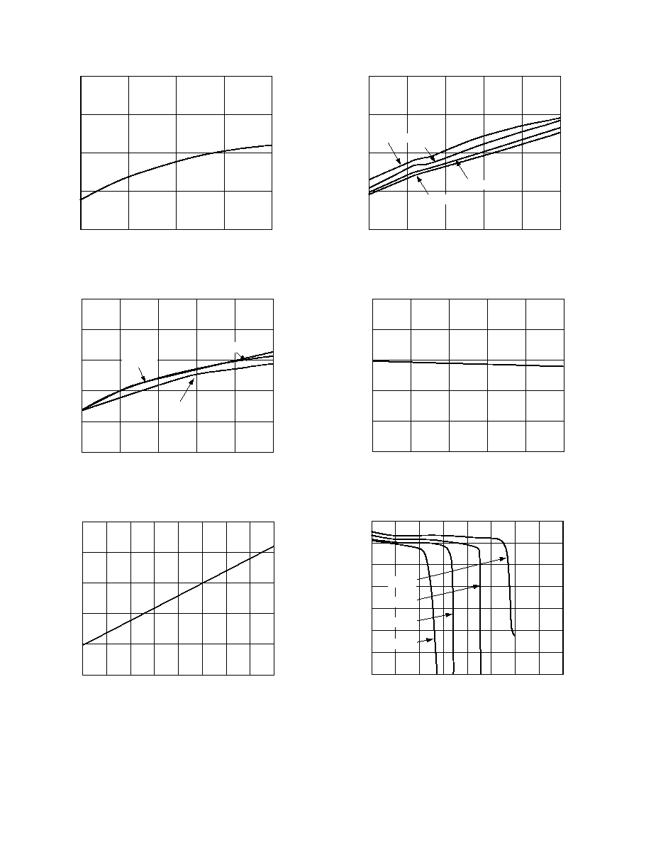
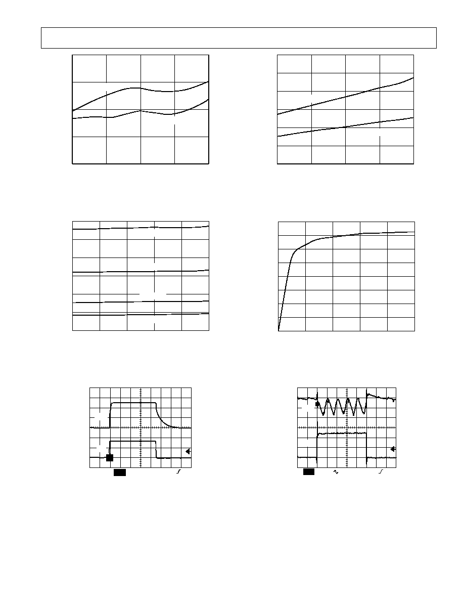
Figure 2. Oscillator Frequency vs. Supply Voltage
TEMPERATURE C
OUTPUT VOLTAGE Volts
4.95
40
15
85
10
35
60
5.03
5.01
4.99
4.97
5.05
I
L
= 50mA
I
L
= 25mA
I
L
= 10mA
Figure 3. Output Voltage vs. Temperature
OUTPUT CURRENT mA
AVERAGE INPUT CURRENT mA
0
10
15
100
75
50
25
125
20
25
30
35
40
45
50
Figure 4. Average Input Current vs. Output Current
4.00
3.75
3.00
40
15
10
35
60
85
TEMPERATURE C
V
IN
= +5.0V
SUPPLY CURRENT mA
3.50
3.25
V
IN
= +4.0V
V
IN
= +3.0V
V
IN
= +3.3V
Figure 5. Supply Current vs. Temperature in Normal Mode
TEMPERATURE C
OSCILLATOR FREQUENCY kHz
200
40
15
85
10
35
60
280
260
240
220
300
Figure 6. Oscillator Frequency vs. Temperature
LOAD CURRENT mA
0
200
100
150
175
OUTPUT VOLTAGE Volts
4.70
5.05
4.75
4.80
4.85
4.90
4.95
5.00
125
75
50
25
V
IN
= +5.0V
V
IN
= +3.3V
V
IN
= +3.0V
V
IN
= +4.0V
Figure 7. Output Voltage vs. Load Current
Typical Performance Characteristics
REV. 0
ADP3607
5
SUPPLY VOLTAGE Volts
SUPPLY CURRENT
A
100
0
3.0
3.5
4.0
4.5
5.0
50
FIXED VERSION
ADJUSTABLE VERSION
R = 38k
150
200
250
300
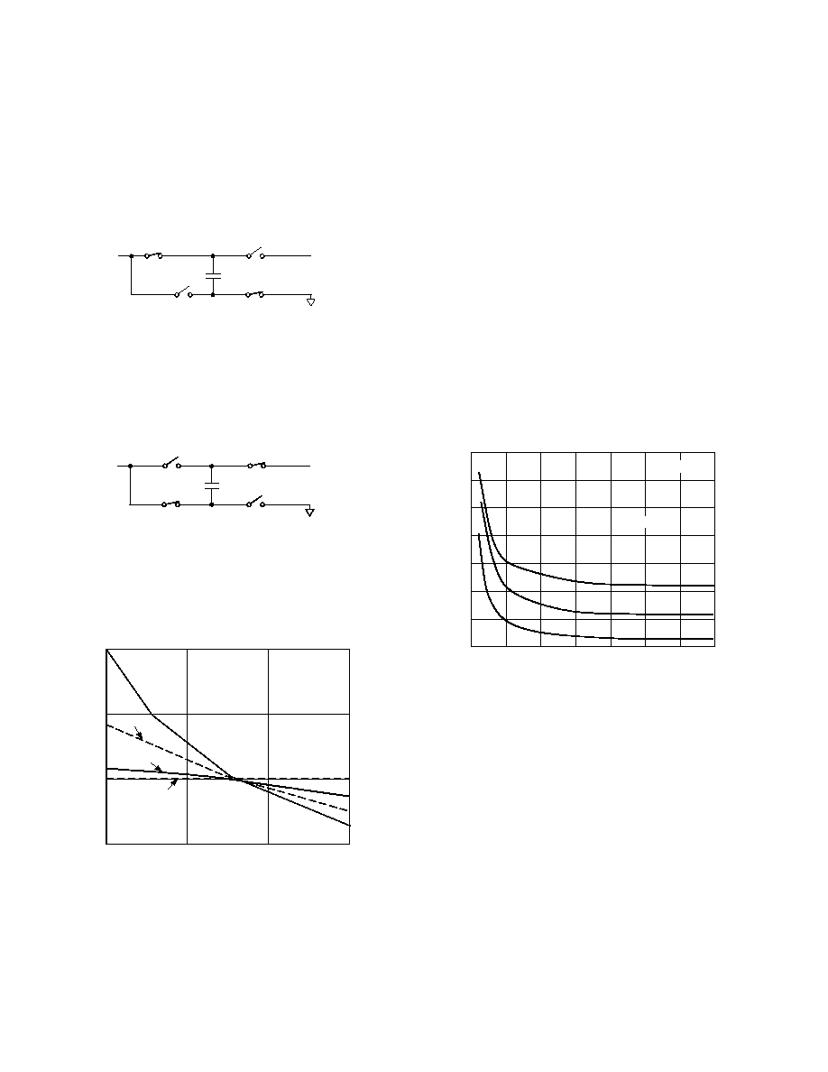
Figure 11. Supply Current vs. Supply Voltage in
Shutdown Mode
LOAD CURRENT mA
0
40
50
EFFICIENCY %
0
30
20
10
10
20
30
40
50
60
70
80
Figure 12. Efficiency vs. Load Current Based on Circuit of
Figure 1
CH2
CH4 10.0mV
20.0mV
CH4
9.0mV
V
O
= +5.0V
V
O
= +4.96V
I
O
= 50mA
I
O
= 1mA
V
OUT
I
L
M4.00 s
B
W
B
W
Figure 13. Load Transient Response Based on Circuit of
Figure 1
SUPPLY VOLTAGE Volts
SUPPLY CURRENT mA
3.6
3.5
3.3
3.0
3.5
4.0
4.5
5.0
3.4
3.7
FIXED VERSION
ADJUSTABLE VERSION
R = 38k
Figure 8. Supply Current vs. Supply Voltage in
Normal Mode
200
180
120
40
15
10
35
60
85
TEMPERATURE C
V
IN
= +5.0V
SUPPLY CURRENT
A
160
140
V
IN
= +4.0V
220
240
V
IN
= +3.3V
V
IN
= +3.0V
Figure 9. Supply Current vs. Temperature in
Shutdown Mode
CH2
CH1 2.00V
2.00V M2.00ms CH2
T
1.12V
V
O
= +5.0V
V
O
= 0V
V
IN
= +3.3V
V
IN
= 0V
V
OUT
V
IN
Figure 10. Start-up Under Full Load Based on Circuit of
Figure 1
REV. 0
ADP3607
6
THEORY OF OPERATION
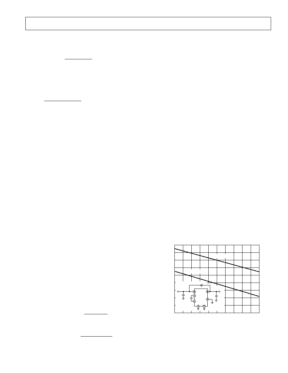
The ADP3607 uses a switched capacitor principle to generate
a regulated boost voltage from a positive input voltage. An
on-board oscillator generates a two-phase clock to control a
switching network that transfers charge between the storage
capacitors. The switches turn on and off at a 250 kHz rate that
is generated from an internal 500 kHz oscillator. The basic
principle behind the voltage conversion scheme is illustrated in
Figures 14 and 15.
S2
S1
V
IN
V
OUT
S3
S4
+
C
P
Figure 14. ADP3607 Switch Configuration Charging the
Pump Capacitor
During phase one, S1 and S3 are ON, charging the pump ca-
pacitor to the input voltage. Before the next phase begins, S1
and S3
are turned OFF, as are S2 and S4 to prevent any over-
lap. S2 and S4
are turned ON during the second phase (see
Figure 15) and charge stored in the pump capacitor is trans-
ferred to the output capacitor.
S2
S1
V
IN
V
OUT
S3
S4
+
C
P
Figure 15. ADP3607 Switch Configuration Charging the
Output Capacitor
During the second phase, the negative terminal of the pump
capacitor is connected to V
IN
through variable resistance switch
S4, and the positive terminal is connected to the output, result-
ing in a voltage shift at the output terminal. The ADP3607
block diagram is shown on the front page.
TEMPERATURE C
10
1.0
0.01
50
100
0
ESR
50
0.1
ALUMINUM
CERAMIC
TANTALUM
ORGANIC SEMIC
Figure 16. ESR vs. Temperature
APPLICATION INFORMATION
Capacitor Selection
The ADP3607's high internal oscillator frequency permits the
use of small capacitors for both the pump and the output ca-
pacitors. For a given load current, factors affecting the output
voltage performance are:
· Pump (C
P
) and output (C
O
) capacitance.
· ESR of the C
P
and C
O
.
When selecting the capacitors, keep in mind that not all manu-
facturers guarantee capacitor ESR in the range required by the
circuit. In general, the capacitor's ESR is inversely proportional
to its physical size, so larger capacitance values and higher volt-
age ratings tend to reduce ESR. Since the ESR is also a function
of the operating frequency, when selecting a capacitor make sure
its value is rated at the circuit's operating frequency. Another
factor affecting capacitor performance is temperature.
Figure 16 illustrates the temperature effect on various capaci-
tors. If the circuit has to operate at temperatures significantly
different from +25
°
C, the capacitance and ESR values must be
carefully selected to adequately compensate for the change.
Various capacitor technologies offer improved performance over
temperature; for example, certain tantalum capacitors provide
good low temperature ESR but at a higher cost. Table II pro-
vides the ratings for different types of capacitor technologies to
help the designer select the right capacitors for the application.
The exact values of C
IN
and C
O
are not critical. However, low
ESR capacitors such as solid tantalum and multilayer ceramic
capacitors are recommended to minimize voltage loss at high
currents. Table III shows a partial list of the recommended low
ESR capacitor manufacturers.
CAPACITANCE F
5
0
20
OUTPUT RIPPLE mV
40
60
80
100
120
140
40
10
ADP3607-5
150m
100m
50m
15
20
25
30
35
I
LOAD
= 50mA
Figure 17. Output Ripple Voltage (mV) vs. Capacitance
and ESR
Input Capacitor
A small 1
µ
F input bypass capacitor (preferably with low ESR)
such as tantalum or multilayer ceramic, is recommended to
reduce noise and supply transients, and supply part of the peak
input current drawn by the ADP3607. A large capacitor is rec-
ommended if the input supply is connected to the ADP3607
through long leads, or if the pulse current drawn by the device
might affect other circuitry through supply coupling.
Output Capacitor
The output capacitor (C
O
) is alternately charged to the C
P
volt-
age when C
P
is switched in parallel with C
O
. The ESR of C
O
introduces steps in the V
OUT
waveform whenever the charge
pump charges C
O
, which contributes to V
OUT
ripple. Thus,
ceramic or tantalum capacitors are recommended for C
O
to
minimize ripple on the output. Figure 17 illustrates the output
ripple voltage effect for various capacitance and ESR values.
Note that as the capacitor value increases beyond the point
where the dominant contribution to the output ripple is due to
the ESR, no significant reduction in V
OUT
ripple is achieved by
added capacitance. Since output current is supplied solely by
REV. 0
ADP3607
7
the output capacitor, C
O
, during one-half of the charge-pump
cycle, peak-to-peak output ripple voltage is calculated by using
the following formula.
V
I
F
C
I
ESR
RIPPLE
L
PUMP
O
L
CO
=
×
×
+ × ×
2
2
where
I
L
= Load Current
F
PUMP
= 250 kHz nominal switching frequency
C
O
= 10
µ
F with an ESR of 0.15
V
mA
kHz
F
mA
RIPPLE
=
×
×
+ ×
×
50
2 250
10
2 50
0 15
µ
.
= 25 mV
Multiple smaller capacitors can be connected in parallel to yield
lower ESR and potential cost savings. For lighter loads, propor-
tionally smaller capacitors are required. To reduce high frequency
noise, bypass the output with a 0.1
µ
F ceramic capacitor in parallel
with the output capacitor.
Pump Capacitor
The ADP3607 alternately charges C
P
to the input voltage when
C
P
is switched in parallel with the input supply, and then trans-
fers charge to C
O
when C
P
is switched in parallel with C
O
. Dur-
ing the time C
P
is charging, the peak current is approximately
two times the output current. During the time C
P
is delivering
charge to C
O
, the supply current drops down to about 3 mA.
A low ESR capacitor has much greater impact on performance
for C
P
than C
O
since current through C
P
is twice the C
O
cur-
rent. Therefore, the voltage drop due to C
P
is about four times
the ESR of C
P
times the load current. While the ESR of C
O
affects the output ripple voltage, the voltage drop generated by
the ESR of C
P
,
combined with the voltage drop due to the out-
put source resistance, determines the maximum available V
OUT
.
Improved Load Regulation
In most applications, IR drops due to printed circuit board
traces are not critical. V
SENSE
should be connected to the output
at a convenient pcb location close to the load. However, if a
reduction in IR drops, or improvement in load regulation is
desired, the sense line can be used to monitor the output voltage
at the load. To avoid excessive noise pickup, keep the V
SENSE
line as short as possible and away from any noisy line.
Shutdown Mode
The ADP3607's output can be disabled by pulling the SD Pin
to a TTL /CMOS logic high level which will stop the internal
oscillator. Applying a logic low will turn ON the oscillator. If
the shutdown feature is not used, the SD pin should be tied to
ground. The shutdown mode current is dominated by the resis-
tor divider connected to the V
SENSE
pin. This current can be
calculated using one of the following formulas.
5 V fixed output version:
I
V
V
k
SENSE SD
IN
(
)
(
.
)
.
=
0 3
23 75
Adjustable output version:
I
V
V
k
R
SENSE SD
IN
EXT
(
)
(
.
)
( .
)
=
+
0 3
9 5
where R
EXT
is in k
.
Because of the external Schottky diode between V
IN
and V
OUT
,
the output voltage will be held to a diode drop below V
IN
when
the ADP3607 is in shutdown mode.
Power Dissipation
The power dissipation of the ADP3607 circuit must be limited
such that the junction temperature of the device does not exceed
the maximum junction temperature rating. Total power dissipa-
tion is calculated as follows:
P = (2 V
IN
V
OUT
) I
OUT
+ (V
IN
) I
S
Where I
OUT
and I
S
are output current and supply current, V
IN
and V
OUT
are input and output voltages respectively.
For example: assuming worst case conditions, V
IN
= 5 V,
V
OUT
= 5 V, I
OUT
= 50 mA and I
S
= 6 mA. Calculated device
power dissipation is:
P
(2
×
5 V 5 V)(0.05 A) + (5 V)(0.006 A) = 280 mW
This is far below the 660 mW power dissipation capability of the
ADP3607.
General Board Layout Guidelines
Since the ADP3607's internal switches turn on and off very
quickly, good PC board layout practices are critical to ensure
optimal operation of the device. Improper layouts will result in
poor load regulation, especially with heavy loads. Following
these simple layout guidelines will improve output performance.
1. Use adequate ground and power traces or planes.
2. Use single point ground for device ground and input and
output capacitor grounds.
3. Keep external components as close to the device as possible.
4. Use short traces from the input and output capacitors
to the input and output pins respectively.
Maximum Output Voltage
Maximum unregulated output voltage can be obtained by con-
necting the V
SENSE
pin to ground instead of to the V
OUT
pin (see
Figure 18). Under this condition, the magnitude of the unregu-
lated output voltage depends on the load current. V
OUT
is
inversely proportional to the load current.
OUTPUT CURRENT mA
5.5
0
OUTPUT VOLTAGE Volts
10
50
5
40
45
35
30
25
20
15
5.7
5.9
6.1
6.3
6.5
6.7
6.9
7.1
7.3
V
IN
= 3.6V
V
IN
= 3.3V
+
V
O
V
IN
C
O
4.7 F
+
C
IN
4.7 F
+
C
P
4.7 F
V
SENSE
V
IN
C
P
+
C
P
V
OUT
GND
D1
IN5819
SD
Figure 18. Maximum Unregulated Output Voltage
REV. 0
ADP3607
8
C350088/99
PRINTED IN U.S.A.
Regulated Adjustable Output Voltage
For the adjustable version of the ADP3607, the regulated out-
put voltage is programmed by a resistor that is inserted between
the V
SENSE
and V
OUT
pins, as illustrated in Figure 19. The in-
herent limit of the output voltage of a single doubling charge
pump stage is two times the input voltage. The scaling factor of
2.00 is reduced somewhat due to losses that increase with out-
put current. To increase the scaling factor to attain a more
positive output voltage, an external pump stage can be added
with just passive components as shown in Figure 20. That single
stage increases the scaling factor to a limit of 3, although the
diode drops will limit the ability to noticeably attain that exact
3.00 scaling factor. Even further increases can be achieved
with more external pump stages. High accuracy on the adjust-
able output is achieved through the use of precision trimmed
internal resistors, which eliminates the need to trim the external
resistor or add a second resistor to form a divider. The adjust-
able output voltage is set using the following formula:
V
R
OUT
=
+
9 5
1
.
where V
OUT
is in volts and R is in k
s.
OUTPUT CURRENT mA
3.5
0
OUTPUT VOLTAGE Volts
10
50
+
V
O
V
IN
= 3.3V
C
O
4.7 F
+
C
IN
4.7 F
+
C
P
4.7 F
V
SENSE
V
IN
C
P
+
C
P
V
OUT
GND
D1
IN5819
SD
R
5
40
45
35
30
25
20
15
4.0
4.5
5.0
5.5
6.0
6.5
R = 47.5k
R = 24.9k
Figure 19. Regulated Adjustable Output Voltage
ADP3607
V
IN
C
P
+
C
P
SD
V
SENSE
V
OUT
GND
+
C
P
4.7 F
C
IN
4.7 F
V
IN
C
O
4.7 F
+
+
C1
4.7 F
D2
SD103
D1
1N5819
+
+
R1
104.5k
C
O2
4.7 F
12V
D3
IN5819
Figure 20. Regulated 12 V from a 5 V Input
Regulated Dual Supply System
The circuit in Figure 21 provides regulated positive and negative
voltages for systems that require dual supplies from a single
battery or power supply.
ADP3607-5
V
IN
C
P
+
C
P
SD
V
SENSE
V
OUT
GND
+
C
P1
10 F
10 F
C
O1
10 F
+
+
+5V
ADP3605
V
IN
C
P
+
C
P
SD
V
SENSE
V
OUT
GND
+
C
P2
10 F
C
O2
10 F
+
R1
16.5k
1%
SD103
V
IN
= +3.3V
2.6V
Figure 21. Regulated Dual Supply System
OUTLINE DIMENSIONS
Dimensions shown in inches and (mm).
8-Lead SOIC
(SO-8)
0.1968 (5.00)
0.1890 (4.80)
8
5
4
1
0.2440 (6.20)
0.2284 (5.80)
PIN 1
0.1574 (4.00)
0.1497 (3.80)
0.0688 (1.75)
0.0532 (1.35)
SEATING
PLANE
0.0098 (0.25)
0.0040 (0.10)
0.0192 (0.49)
0.0138 (0.35)
0.0500
(1.27)
BSC
0.0098 (0.25)
0.0075 (0.19)
0.0500 (1.27)
0.0160 (0.41)
8°
0°
0.0196 (0.50)
0.0099 (0.25)
x 45°
8-Lead TSSOP
(RU-8)
8
5
4
1
0.256 (6.50)
0.246 (6.25)
0.177 (4.50)
0.169 (4.30)
PIN 1
0.0256 (0.65)
BSC
0.122 (3.10)
0.114 (2.90)
SEATING
PLANE
0.006 (0.15)
0.002 (0.05)
0.0118 (0.30)
0.0075 (0.19)
0.0433
(1.10)
MAX
0.0079 (0.20)
0.0035 (0.090)
0.028 (0.70)
0.020 (0.50)
8
0