 | ÐлекÑÑоннÑй компоненÑ: ADP3604 | СкаÑаÑÑ:  PDF PDF  ZIP ZIP |
Äîêóìåíòàöèÿ è îïèñàíèÿ www.docs.chipfind.ru
REV. 0
Information furnished by Analog Devices is believed to be accurate and
reliable. However, no responsibility is assumed by Analog Devices for its
use, nor for any infringements of patents or other rights of third parties
which may result from its use. No license is granted by implication or
otherwise under any patent or patent rights of Analog Devices.
a
Switched Capacitor Voltage Converter
with Regulated Output
ADP3604*
© Analog Devices, Inc., 1996
One Technology Way, P.O. Box 9106, Norwood, MA 02062-9106, U.S.A.
Tel: 617/329-4700
Fax: 617/326-8703
GENERAL DESCRIPTION
The ADP3604 switched capacitor voltage converter provides a
regulated output voltage with minimum voltage loss and re-
quires a minimum number of external components. In addi-
tion, the ADP3604 does not require the use of an inductor.
The ADP3604 provides up to 120 mA of output current with
±
3% output accuracy.
The internal oscillator runs at 240 kHz nominal frequency
which produces an output switching frequency of 120 kHz, al-
lowing the use of small charge pump and filter capacitors.
The ADP3604 is primarily designed for use as a high fre-
quency negative voltage regulator/inverter. The output voltages
of the ADP3604 can range from 1.2 V to 4.0 V, nominally
3.0 V. For other output voltages, contact the factory.
The ADP3604 dissipates less than 350 mW of power and fea-
tures fast shutdown mode capability (<5 ms) that also drops the
quiescent current to 1.5 mA (typ). For a lower cost, 50 mA out-
put current version, see the ADP3603.
*Patent pending.
FEATURES
Fully Regulated Output
High Output Current: 120 mA
50 mA Version (ADP3603) Is Also Available
Outstanding Precision: 3% Output Accuracy
Input Voltage Range: +4.5 V to +6.0 V
Output Voltage: 3.0 V (Regulated)
High Switching Frequency: 120 kHz (240 kHz Internal
Oscillator)
Shutdown Capability
Small Outline 8-Pin SOIC Package
APPLICATIONS
Voltage Inverters
Voltage Regulators
Computer Peripherals and Add-On Cards
Portable Instruments
Battery Powered Devices
Pagers and Radio Control Receivers
Disk Drives
Mobile Phones
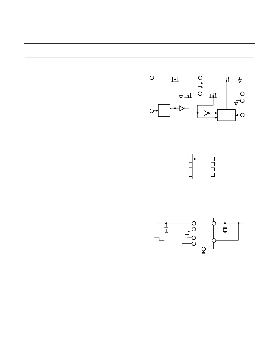
FUNCTIONAL BLOCK DIAGRAM
8
S P D
S1
S N D
S2
S
N
D
B
S3
S
N
D
7
3
V
IN
C
P
C
P
+
1
S4
2
V
OUT
GND
OSC
CLOCK
GEN
4
SD
FEEDBACK
CONTROL
LOOP
5
V
SENSE
PIN CONFIGURATION
8-Pin SOIC
(SO-8)
1
2
3
4
8
7
6
5
TOP VIEW
(Not to Scale)
NC = NO CONNECT
ADP3604
C
P
+
V
SENSE
NC
V
OUT
V
IN
GND
C
P
SHUTDOWN
ADP3604
8
7
3
C2
4.7µF
1
4
SHUTDOWN
0
OFF
ON
C1
4.7µF
V
IN
+4.5 +6V
V
OUT
3.0V
C3
4.7µF
2
5
V
SENSE
NOTE
C2: SPRAGUE, 293D105X0010B2W
C1, C3: TOKIN, 1E105ZY5UC205F
FOR BEST PERFORMANCE 10µF IS RECOMMENDED
Figure 1. Typical Application Circuit
PIN DESCRIPTION
Pin
Function
1
C
P
+, Pump Capacitor Positive Input.
2
Ground.
3
C
P
, Pump Capacitor Negative Input.
4
Shutdown, Logic Level Shutdown Pin. Application of a
logic low to this pin will place the regulator in normal
operation. The device will be put into shutdown mode
with the shutdown pin pulled to V
IN
. In Shutdown
mode the charge pump is turned off. Connect to ground
for normal operation.
5
V
SENSE
, Output Voltage Sense Line. This is used to im-
prove load regulation performance by eliminating IR
drop on the output traces. See application section for
more detail. For normal operation, connect Pin 5 to
V
OUT
(Pin 7).
6
NC, No Internal Electrical Connection.
7
V
OUT,
Output Pin. Regulated negative output voltage.
Connect a low ESR capacitor between this pin and de-
vice GND.
8
V
IN,
Positive Supply Input when 4.5 V
V
IN
6 V.
Connect a low-ESR bypass capacitor between this pin
and the device ground pin.
Parameter
Symbol
Condition
Min
Typ
Max
Units
OPERATING SUPPLY RANGE
V
S
4.5
5
6
V
SUPPLY CURRENT
I
S
2.9
3.5
mA
40
°
C < T
A
< +85
°
C
3
4
mA
Shutdown Mode
1.5
2.5
mA
40
°
C < T
A
< +85
°
C
1.6
3.0
mA
OUTPUT
Output Voltage
V
O
I
O
= 60 mA
3.1
3.0
2.91
V
V
O
I
O
= 10 mA to 120 mA, 4.5 V < V
IN
< 6 V
3.1
3
2.88
V
V
O
I
O
= 10 mA to 120 mA, 4.5 V < V
IN
< 6 V,
0
°
C < T
A
< +70
°
C
3.12
3
2.85
V
V
O
I
O
= 10 mA to 120 mA, 4.5 V < V
IN
< 6 V,
40
°
C < T
A
< +85
°
C
3.2
3
2.8
V
Load Regulation
V
O
/ I
O
I
O
= 10 mA60 mA
0.9
mV/mA
I
O
= 10 mA120 mA
1.5
mV/mA
Output Resistance
2
R
O
8
Output Ripple Voltage
3
V
RIPPLE
C1C3 = 10
µ
F, I
LOAD
= 80 mA
25
mV
C1C3 = 10
µ
F,
I
LOAD
= 120 mA
55
mV
SWITCHING FREQUENCY
F
S
100
120
135
kHz
40
°
C < T
A
< +85
°
C
96
120
140
kHz
SHUTDOWN
Logic Input High
V
IH
2.4
V
Input Current
I
IH
1
µ
A
Logic Input Low
V
IL
0.4
V
Input Current
I
IL
1
µ
A
Turn-On-Time
t
ON
Figure 1, I
L
= 120 mA
5
ms
Turn-Off-Time
t
OFF
Figure 1, I
L
= 120 mA
5
ms
NOTES
1
Capacitors C1 and C2 used in the test circuit are 10
µ
F with 0.1
ESR. Capacitors with higher ESR may reduce output voltage and efficiency.
2
Open-loop output resistance.
3
See Figure 1 conditions.
All limits at temperature extremes are guaranteed via correlation using standard Statistical Quality Control (SQC) methods.
Specifications subject to change without notice
.
REV. 0
2
ADP3604SPECIFICATIONS
WARNING!
ESD SENSITIVE DEVICE
CAUTION
ESD (electrostatic discharge) sensitive device. Electrostatic charges as high as 4000 V readily
accumulate on the human body and test equipment and can discharge without detection.
Although the ADP3604 features proprietary ESD protection circuitry, permanent damage may
occur on devices subjected to high energy electrostatic discharges. Therefore, proper ESD
precautions are recommended to avoid performance degradation or loss of functionality.
(V
IN
= 5.0 V @ T
A
= +25 C, C
P
= C
OUT
= 10 F unless otherwise noted)
ABSOLUTE MAXIMUM RATINGS
1
(T
A
= +25
°
C unless otherwise noted)
Input Voltage (V+ to GND, GND to OUT) . . . . . . . . . +7.5 V
Output Short Circuit Protection . . . . . . . . . . . . . . . . . . . . 1 sec
Power Dissipation, SO-8 . . . . . . . . . . . . . . . . . . . . . . . 660 mW
JA
2
. . . . . . . . . . . . . . . . . . . . . . . . . . . . . . . . . . . . . 150
°
C/W
JC
. . . . . . . . . . . . . . . . . . . . . . . . . . . . . . . . . . . . . . 41
°
C/W
Operating Temperature Range . . . . . . . . . . . . . 40
°
C to +85
°
C
Storage Temperature Range . . . . . . . . . . . . . 65
°
C to +150
°
C
Lead Temperature Range (Soldering 10 sec) . . . . . . . . +300
°
C
Vapor Phase (60 sec) . . . . . . . . . . . . . . . . . . . . . . . . +215
°
C
Infrared (15 sec) . . . . . . . . . . . . . . . . . . . . . . . . . . . . +220
°
C
NOTES
1
This is a stress rating only and functional operation of the device at these or any
other conditions above those indicated in the operation section of this specification
is not implied. Exposure to absolute maximum rating conditions for extended
periods may affect device reliability.
2
JA
is specified for worst case conditions with device soldered on a circuit board.
ORDERING GUIDE
Model
Temperature Range
Package Option*
ADP3604AR
40
°
C to +85
°
C
SO-8
*SO = Small Outline Package.
ADP3604
REV. 0
3
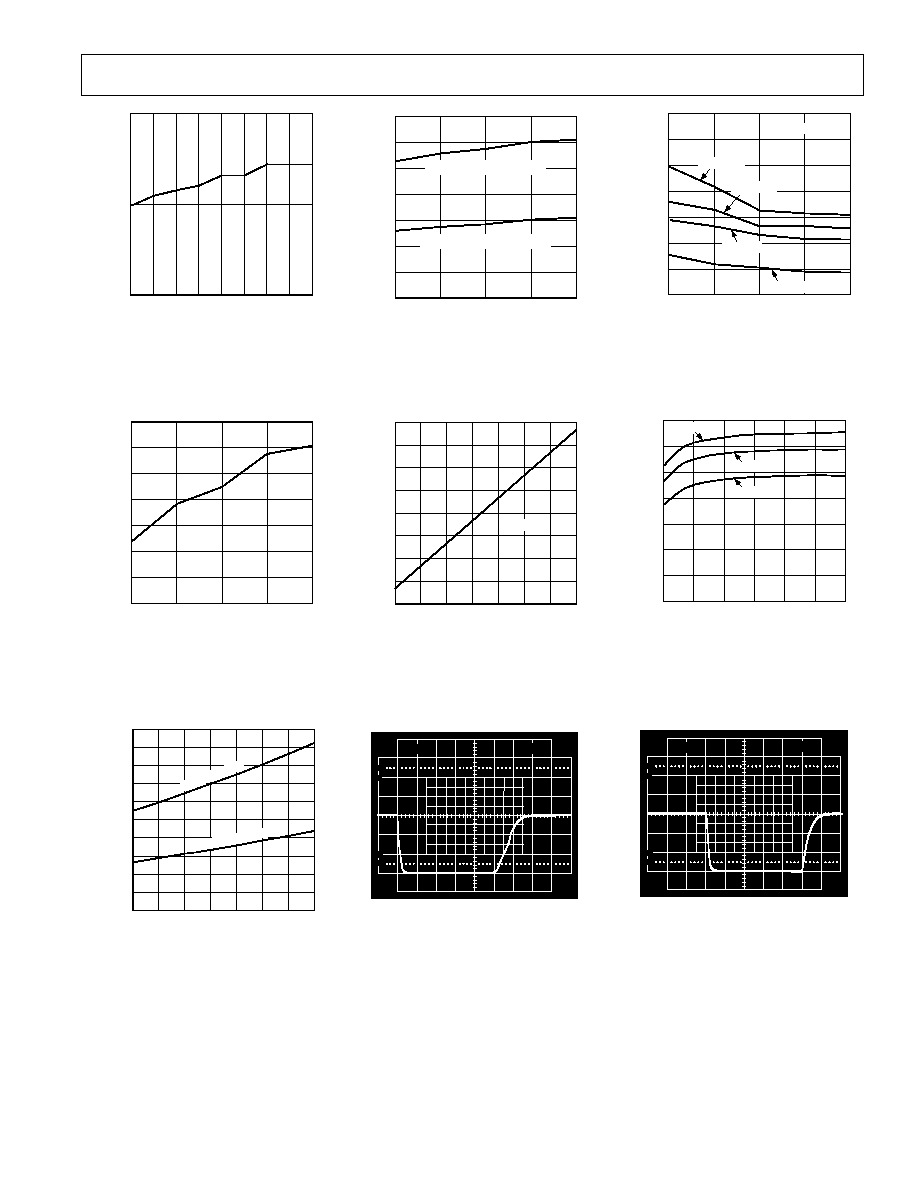
SUPPLY VOLTAGE V
OSCILLATOR FREQUENCY kHz
130
120
110
4.0
4.5
8.0
5.0
5.5
6.0
6.5
7.0
7.5
Figure 2. Oscillator Frequency vs.
Supply Voltage
TEMPERATURE
°
C
OSCILLATOR FREQUENCY kHz
126
112
40
85
0
25
70
124
122
120
118
116
114
V
IN
= 5V
Figure 5. Oscillator Frequency vs.
Temperature
SUPPLY VOLTAGE V
SUPPLY CURRENT mA
5.0
2.5
0
4.5
5.0
8.0
5.5
6.0
7.0
7.5
6.5
4.5
2.0
4.0
1.5
3.5
1.0
3.0
0.5
NORMAL MODE
SHUTDOWN MODE
Figure 8. Supply Current vs. Supply
Voltage
TEMPERATURE
°
C
SUPPLY CURRENT mA
3.5
3.0
0
40
85
0
25
70
2.5
2.0
1.5
1.0
0.5
NORMAL MODE @ V
IN
= 5V
SHUTDOWN MODE @ V
IN
= 5V
Figure 3. Supply Current vs.
Temperature
LOAD CURRENT mA
INPUT CURRENT mA
160
80
0
10
30
50
70
90
140
120
100
60
40
20
110
130
150
V
IN
= 5V
Figure 6. Average Input Current vs.
Load Current
100
90
10
0%
1V
2mS
0V
0V
Figure 9. Start-Up Under Full Load
TEMPERATURE
°
C
OUTPUT VOLTAGE V
2.9
3.04
40
85
0
25
70
2.92
2.94
2.96
2.98
3.00
3.02
V
IN
= 5V
I
L
= 150mA
I
L
= 120mA
I
L
= 60mA
I
L
= 10mA
Figure 4. Output Voltage vs.
Temperature
LOAD CURRENT mA
EFFICIENCY %
70
60
0
10
30
130
50
90
110
70
50
40
30
20
10
V
IN
= 4.5V
V
IN
= 5.0V
V
IN
= 6.0V
Figure 7. Efficiency vs. Load
Current and Input Voltage
100
90
10
0%
1V
2mS
0V
0V
Figure 10. Enable/Disable Time
Under Full Load
ADP3604
REV. 0
4
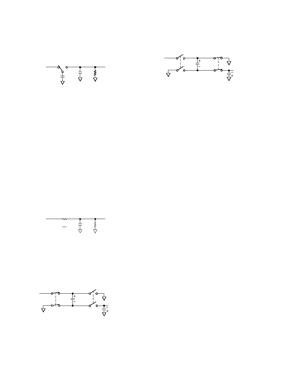
APPLICATION INFORMATION
The ADP3604 uses a charge pump to generate a negative out-
put voltage from a positive input supply. To understand the
operation of the ADP3604, a review of a basic switch capacitor
building block is helpful.
f
R
L
V1
V2
C1
C2
A
B
Figure 11. Basic Switch Capacitor Circuit
In Figure 11, when the switch is in the A position, capacitor C1
will be charged to voltage V1. The total charge on C1 will be
q1 = C1V1.
The switch then moves to the B position, discharging C1 to
voltage V2. After this discharge time, the charge on C1 is q2 =
C1V2. The amount of charge transferred from the source, V1,
to the output, V2 is:
q = q1 q2 = C1(V1 V2)
If the switch is cycled f times per second, the charge transfer
per unit time (i.e., current) is:
I = f
q = fC1(V1 V2)
To obtain an equivalent resistance for the switched-capacitor
network we can rewrite this equation in terms of voltage and
impedance equivalence:
I = (V1 V2)/(1/fC1) = (V1 V2)/R
EQUIV
where R
EQUIV
is defined as :
R
EQUIV
= 1/fC1
Figure 11 equivalent circuit now can be drawn as shown in
Figure 12.
R
L
V1
V2
C2
R
EQUIV
R
EQUIV =
1
fC1
Figure 12. Basic Switch Capacitor Equivalent Circuit
THEORY OF OPERATION
A switched capacitor principle is used in the ADP3604 to gener-
ate a negative voltage from a positive input voltage. An on-board
oscillator generates two phase clocks to control a switching net-
work which transfers charge between the storage capacitors.
The basic principle behind the voltage inversion scheme is illus-
trated in Figures 13 and 14.
V
IN
S2
C
P
S1
V
OUT
S3
S4
C
OUT
Figure 13. Switch Configuration Charging the Pump
Capacitor
During phase one, S1 and S2 are ON charging the pump ca-
pacitor to the input voltage. Before the next phase begins, S1
and S2
are turned OFF as well as S3 and S4 to prevent any
overlap. S3 and S4
are turned ON during the second phase (see
Figure 14) and charge stored in the pump capacitor is trans-
ferred to the output capacitor.
V
IN
S2
C
P
S1
V
OUT
S3
S4
C
OUT
Figure 14. Switch Configuration Charging the Output
Capacitor
During the second phase, the positive terminal of the pump
capacitor is connected to ground and the negative terminal is
connected to the output resulting in a voltage inversion at the
output terminal. Output regulation is done by adjusting the ON
resistance of the S3 through the feedback control loop.
The ADP3604 alternately charges C
P
to the input voltage when
C
P
is switched in parallel with the input supply, and then trans-
fers charge to C
OUT
when C
P
is switched in parallel with C
OUT
.
Switching occurs at 120 kHz rate. During the time that C
P
is
charging, the peak current is approximately 2 times the output
current. During the time that C
P
is delivering charge to C
OUT
,
the supply current drops down to about 2 mA. An input supply
bypass capacitor will supply part of the peak input current drawn
by the ADP3604, and average out the current drawn from the
supply. A minimum input supply bypass capacitor of 1
µ
f,
preferably a low ESR capacitor such as tantalum or multilayer
ceramic chip capacitor, is recommended. A large capacitor may
be desirable in some cases, for example when the input supply is
connected to the ADP3604 through long leads, or when the
pulse current drawn by the device might effect other circuitry
through supply coupling.
The output capacitor, C
OUT
, is alternately charged to the C
P
voltage when C
P
is switched in parallel with C
OUT
. The ESR of
the C
OUT
introduces steps in the V
OUT
waveform whenever the
charge pump charges C
OUT
. This tends to increase V
OUT
ripple.
Ceramic or tantalum capacitors are recommended for C
OUT
if
minimum ripple is desired. The ADP3604 can operate with a
range of capacitors from 1
µ
f to 100
µ
f and larger without any
stability problems. However, all tested parameters are obtained
using 10
µ
f multilayer ceramic capacitors.
In most applications, IR drops due to printed circuit board
traces do not present a problem. In this case, V
SENSE
is tied to
the output at a convenient pcb location not far from the V
OUT
.
However, if a reduction in IR drops or improvement in load
regulation is desired, the sense line can be used to monitor the
output voltage at the load. To avoid excessive noise pickup, the
V
SENSE
line should be as short as possible and away from any
noisy line.
While the exact values of the C
IN
and C
OUT
are not critical, good
quality, low ESR capacitors such as solid tantalum and multi-
layer ceramic capacitors are recommended to minimize voltage
losses at high currents. For a given load current, factors affecting
the output voltage performance in Figure 15 are:
· Pump (C2) and the output (C3) capacitance
· ESR of the C2 and C3
ADP3604
REV. 0
5
TEMPERATURE
°
C
ESR
10
1.0
0.01
50
100
0
50
0.1
ALUMINUM
CERAMIC
ORGANIC SEMIC
TANTALUM
ALUMINUM
CERAMIC
ORGANIC SEMIC
TANTALUM
Figure 16. ESR vs. Temperature
Table I. Alternative Capacitor Technologies
High
Type
Life
Freq
Temp
Size
Cost
Aluminum
Fair Fair
Fair
Small
Low
Electrolytic
Capacitor
Multilayer
Long
Good
Poor
Fair
High
Ceramic
Capacitor
Solid
Above
Avg
Avg
Avg
Avg
Tantalum
Avg
Capacitor
OS-CON
Above
Good
Good
Good
Avg
Capacitor
Avg
The following is a partial list of manufacturers providing low
ESR capacitors.
Table II. Recommended Capacitor Manufacturers
Manufacturer
Capacitor
Capacitor Type
Sprague
672D, 673D,
Aluminum Electrolytic
674D, 678D
Sprague
675D, 173D,
Tantalum
199D
Nichicon
PF & PL
Aluminum Electrolytic
Mallory
TDC & TDL
Tantalum
TOKIN
MLCC
Multilayer Ceramic
muRata
GRM
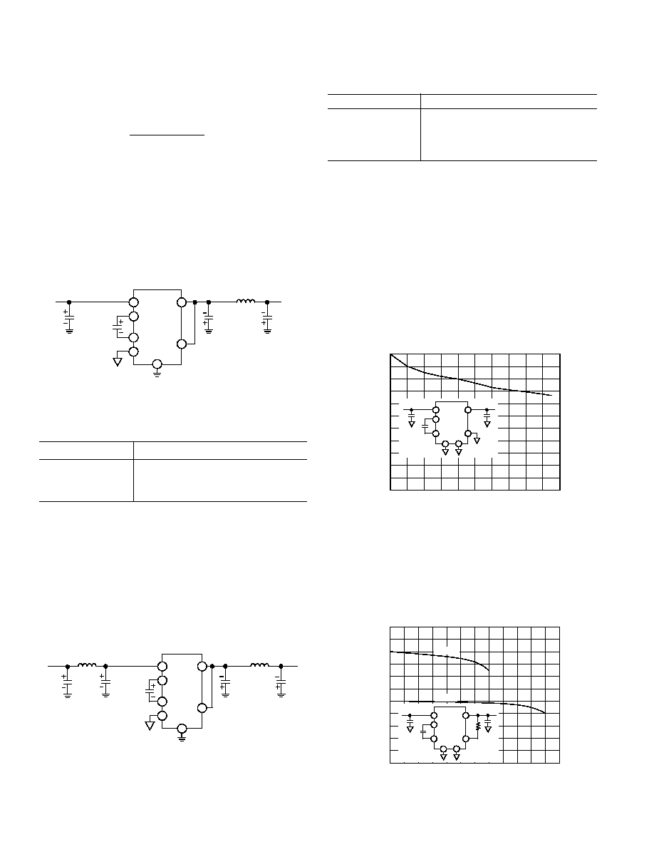
Multilayer Ceramic
EXTERNAL OUTPUT FILTERING
In applications requiring very low power supply ripple and
noise, the circuit in Figure 18 provides low noise and ripple of
less than 2% of the output voltage over the full load current and
temperature.
Since output current is supplied solely by the output capacitor
C3 during one-half of the charge-pump cycle, peak-to-peak
output ripple voltage is calculated by using the following
formula:
V
RIPPLE
=
I
OUT
2(F
PUMP
)(C2)
+
I
OUT
(ESR
C2
)
In Figure 15, output ripple voltage vs. capacitance and various
ESR are shown.
CAPACITANCE µF
OUTPUT RIPPLE mV
120
0
0
180
20
40
60
80
100
120
140
160
100
80
60
40
20
ESR
C
140mA
V
OUT
ADP3604
150m
100m
50m
Figure 15. Output Ripple Voltage (mV) vs. Capacitance
and ESR
Note that as the capacitor value increases beyond the point
where the dominant contribution to the output ripple is due to
the ESR, no significant reduction in V
OUT
ripple is achieved by
added capacitance.
A low ESR capacitor has much greater impact on performance
for C2 than C3 since current through C2 is twice the C3 cur-
rent. There is a voltage drop across C
P
's ESR during the charge
as well as during discharges. Therefore, the voltage drop due to
C2 is about 4 times C2's ESR times the load current. The volt-
age drop generated by C2's ESR combined with the voltage
drop due to the output source resistance, determines the maxi-
mum available V
OUT
, while C3's ESR affects the output voltage
ripple.
When selecting the capacitors, keep in mind that not all manu-
facturers guarantee capacitor ESR in the range required by the
circuit. In general, the capacitor's ESR is inversely proportional
to its physical size, so larger capacitance values and higher volt-
age ratings tend to reduce ESR.
ESR is also a function of the operating frequency. When select-
ing a capacitor, make sure its value is rated at the circuit's oper-
ating frequency. The other factor affecting the capacitor's
performance is temperature. If the circuit has to operate at tem-
peratures significantly different than 25
°
C, the capacitance and
ESR values must be carefully selected to adequately compen-
sate for the change. Various capacitor technologies offer im-
proved performance over temperature, for example, certain
tantalum capacitors provide good low-temperature ESR but at
a higher cost.
Figure 16 demonstrates the effect temperature has on various
capacitors. ADP3604's high internal oscillator frequency per-
mits the usage of smaller capacitance for both the pump and
the output capacitors.
ADP3604
REV. 0
6
The output current is supplied solely by the output capacitor
C3 during one-half of the charge-pump cycle. This introduces a
peak-to-peak ripple of:
V
RIPPLE
=
I
L
2
×
120 kHz
×
C3
+
I
L
×
ESR
C3
For a nominal F pump of 120 kHz (one-half the nominal 240 kHz
oscillator frequency) and C3 = 10
µ
F with an ESR of 0.15
,
ripple voltage is approximately 60 mV with a 120 mA load
current.
Multilayer Ceramic Capacitors (MLCC) offer great perfor-
mance and small size. Using multiple capacitors connected in
parallel yields lower ESR and a potential saving in cost. Lighter
loads require proportionally smaller capacitors. To reduce high
frequency noise, bypass the output with a 0.1
µ
F ceramic
capacitor.
ADP3604
8
7
3
C2
4.7µF
1
4
V
IN
+4.5 +6V
V
OUT
3.0V
C3
4.7µF
2
5
SENSE
INPUT
L1
10µH
C4
4.7µF
C1
4.7µF
Figure 17. Circuit with Improved Output Ripple & Noise
Voltage
Table III. Recommended Components for Circuit in Figure 17
Component
Manufacturer/Type
C2
Sprague, 293D475X0035D2W
C1, C3, C4
TOKIN, 1E475ZY5U-C205-F
L1
Coiltronics, CTX32CT
EXTERNAL INPUT FILTERING
If the ADP3604 is supplied from an high-impedance source,
connect an additional bypass capacitor from V+ to ground.
Low-ESR capacitors of up to 100
µ
F give best results. Place
external capacitors close to the supply pins of the device with
the ground connection made as close to the device ground as
possible. The same ground point should be used for the output
bypass capacitor.
Smaller bypass capacitors can be used in conjunction with a
-LC filter.
ADP3604
8
7
3
C3
4.7µF
1
4
V
IN
+4.5 +6V
V
OUT
3.0V
C4
4.7µF
2
5
SENSE
INPUT
L2
10µH
C5
4.7µF
C2
4.7µF
L1
1µH
C1
4.7µF
Figure 18. Circuit with Reduced Input and Output Ripple
& Noise Voltage
Table IV. Recommended Components for Circuit in Figure 18
Component
Manufacturer/Type
C3
Sprague, 293D475X0035D2W
C1, C2, C4, C5
TOKIN, 1E475ZY5UC205F
L1
Coiltronics, CTX32CT-1R0
L2
Coiltronics, CTX32CT-100
SHUTDOWN MODE
ADP3604's output can be turned off by utilizing the shutdown
pin, Pin 4. Pulling the shutdown pin high to a TTL/CMOS
logic compatible level will stop the internal oscillator and turn
OFF the output pass transistor. A digital low level will turn the
output ON. If the shutdown feature of the device is not used,
Pin 4 should be tied to the ground pin of the device.
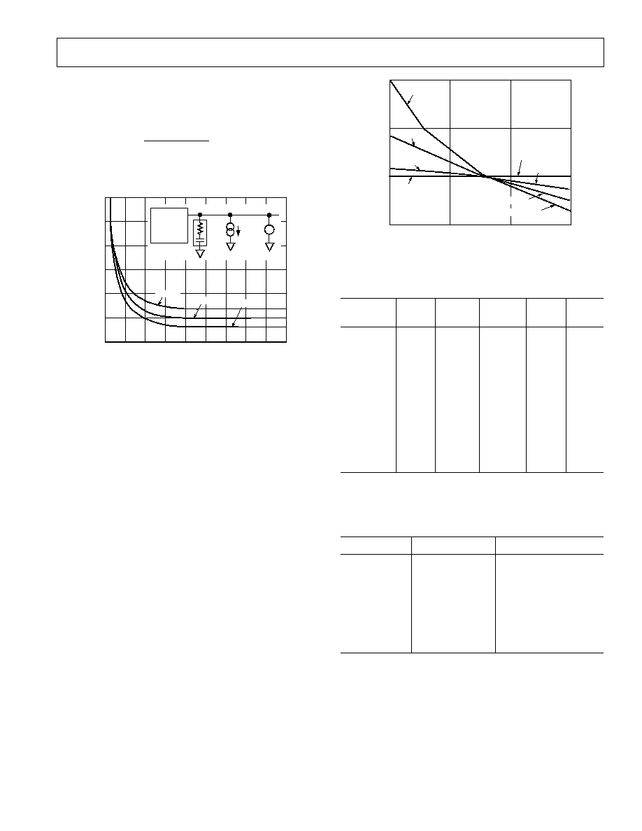
MAXIMUM OUTPUT VOLTAGE
Maximum unregulated output voltage can be obtained by con-
necting the sense pin to ground instead of the V
OUT
pin as
shown in Figure 19.
Under this condition, the magnitude of the unregulated output
voltage depends on the load current. V
OUT
is inversely propor-
tional to the load current as shown on the graph in Figure 19.
LOAD CURRENT mA
5.0
4.0
10
90
V
OUT
Volts
30
50
70
3.0
ADP3604
8
7
3
1
4
V
IN
= 5.0V
2
5
Figure 19. Maximum Unregulated Output Voltage
Under light loads, 30 mA < I
LOAD
, a regulated output voltage
between 3.0 V to V
IN
V is possible by inserting a resistor be-
tween the sense pin and the V
OUT
pin as shown in Figure 20.
The output voltage is approximated using the following formula:
V
OUT
= (3 +R/5)
where V
OUT
is in volts and R is in k
s.
LOAD CURRENT mA
5.0
4.0
10
90
V
OUT
Volts
30
50
70
3.0
ADP3604
8
7
3
1
4
V
IN
= 5.0V
2
5
V
OUT
R
R = 10k
R = 5k
110
Figure 20. Maximum Regulated Output Voltage
ADP3604
REV. 0
7
POWER DISSIPATION
The power dissipation of the ADP3604 circuit must be limited
such that the junction temperature of the device does not ex-
ceed the maximum junction temperature rating.
Power is dissipated in two components, power loss due to volt-
age drops in the switches, and the power loss due to MOSFET
drive current losses. Total power dissipation is calculated:
P
(V
IN
|V
OUT
|)(I
OUT
) + (V
IN
)(I
S
)
where both V
IN
and V
OUT
are referred to ground pin of the
ADP3604.
For example: Assuming the worst case conditions, V
IN
= 5.5 V,
V
OUT
= 2.8 V, and I
OUT
= 120 mA, calculated power dissipa-
tion is:
P
(5.5 V|2.8 V|)(0.12) + (5.5 V)(0.003 A) = 341 mW
This is far below the power dissipation capability of the
ADP3604 package which is 660 mW.
LAYOUT AND GROUNDING TIPS
The ADP3604 switches turn on and off very fast. Good PC
board layout practices will ensure the proper operation of the
device. Important layout considerations include:
Use adequate ground and power traces or planes.
Keep components as close as possible to the device.
Use short trace lengths from the input and output capacitors to
the input and output pins respectively.
Use single point ground for the device ground pins and the in-
put and output capacitors.
Improper layouts will result in poor load regulation, especially
with heavy loads.
APPLICATIONS
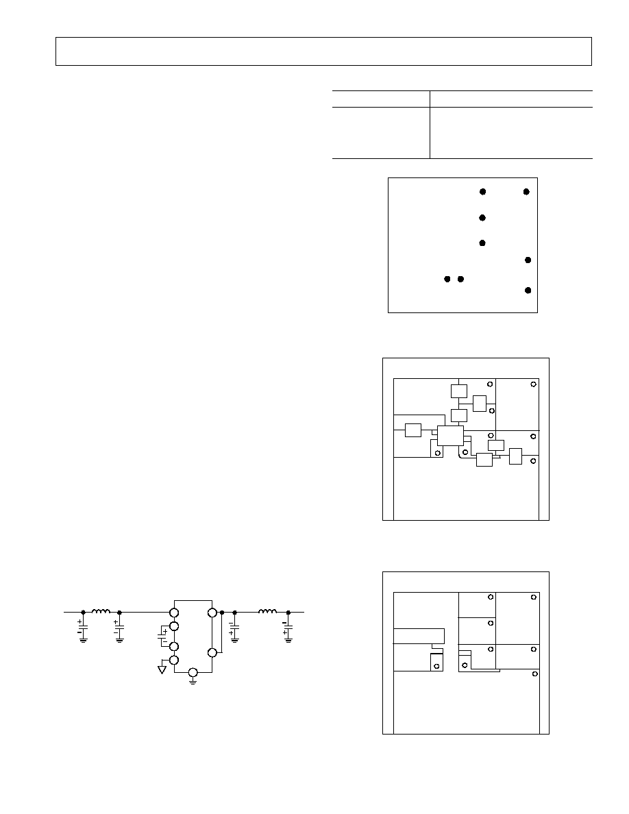
ADP3604 EVALUATION BOARD LAYOUT
The ADP3604 evaluation board is a general purpose circuit
board. Its flexible design allows the user to optimize the circuit
performance by external components selection and circuit con-
figuration. The circuit board can be configured as a basic charge
pump voltage inverter with one pump capacitor and two bypass
capacitors or as a more complex circuit with input and output
LC filters.
PC layout is designed for surface mount components and can
be easily configured for through hole components as well.
ADP3604
8
7
3
C3
4.7µF
1
4
V
IN
+4.5 +6V
V
OUT
3.0V
C4
4.7µF
2
5
SENSE
INPUT
L2
10µH
C5
4.7µF
C2
4.7µF
L1
1µH
C1
4.7µF
Figure 21. Evaluation Board Circuit Diagram
C2
C1
C4
C5
L1
C3
L2
Figure 23. Eight-Pin SOIC-Layout, Component Placement
Diagram (1
×
Scale)
Figure 24. Eight-Pin-SOIC Layout, Component Side
(1
×
Layout)
Table V. Recommended Components for Circuit in Figure 21
Component
Manufacturer/Type
C3
Sprague, 293D475X0035D2W
C1, C2, C4, C5
TOKIN, 1E475ZY5UC205F
L1
Coiltronics, CTX32CT-1R0
L2
Coiltronics, CTX32CT-100
FILTERED INPUT
INPUT
OUTPUT
FILTERED OUTPUT
SHDN
OUTPUT GND
Figure 22. Eight-Pin SOIC Layout, Wiring Connection
ADP3604
REV. 0
8
C2170129/96
PRINTED IN U.S.A.
OUTLINE DIMENSIONS
Dimensions shown in inches and (mm).
8-Pin SOIC
(SO-8)
0.1968 (5.00)
0.1890 (4.80)
8
5
4
1
0.2440 (6.20)
0.2284 (5.80)
PIN 1
0.1574 (4.00)
0.1497 (3.80)
0.0688 (1.75)
0.0532 (1.35)
SEATING
PLANE
0.0098 (0.25)
0.0040 (0.10)
0.0192 (0.49)
0.0138 (0.35)
0.0500
(1.27)
BSC
0.0098 (0.25)
0.0075 (0.19)
0.0500 (1.27)
0.0160 (0.41)
8
°
0
°
0.0196 (0.50)
0.0099 (0.25)
x 45
°