 | ÐлекÑÑоннÑй компоненÑ: ADP3402 | СкаÑаÑÑ:  PDF PDF  ZIP ZIP |
Äîêóìåíòàöèÿ è îïèñàíèÿ www.docs.chipfind.ru
REV. 0
Information furnished by Analog Devices is believed to be accurate and
reliable. However, no responsibility is assumed by Analog Devices for its
use, nor for any infringements of patents or other rights of third parties
which may result from its use. No license is granted by implication or
otherwise under any patent or patent rights of Analog Devices.
a
ADP3402
One Technology Way, P.O. Box 9106, Norwood, MA 02062-9106, U.S.A.
Tel: 781/329-4700
World Wide Web Site: http://www.analog.com
Fax: 781/326-8703
© Analog Devices, Inc., 2000
FEATURES
Handles all GSM Baseband Power Management
Functions
Four LDOs Optimized for Specific GSM Subsystems
Charges Back-Up Capacitor for Real-Time Clock
Charge Pump and Logic Level Translators for 3 V and 5 V
GSM SIM Modules
Thermally Enhanced 6.1 mm 28-Lead TSSOP Package
APPLICATIONS
GSM/DCS/PCS Handsets
TeleMatic Systems
ICO/Iridium Terminals
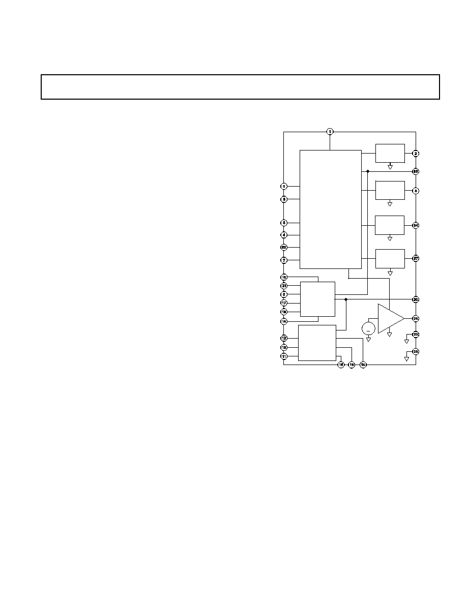
GSM Power Management System
FUNCTIONAL BLOCK DIAGRAM
DIGITAL
LDO
VCC
VRTC
VTCXO
PWRONKEY
ROWX
PWRONIN
RESET
ANALOGON
POWER-UP
SEQUENCING
AND
PROTECTION
LOGIC
ADP3402
VBAT
REFOUT
AGND
VCCA
RESCAP
CHRON
SIMBAT
CAP+
CAP
SIMPROG
SIMON
SIMGND
RESETIN
CLKIN
DATAIO
CHARGE
PUMP
LOGIC LEVEL
TRANSLATION
BUFFER
REF
+
I/O
RST
CLK
VSIM
RTC LDO
XTAL OSC
LDO
ANALOG
LDO
DGND
GENERAL DESCRIPTION
The ADP3402 is a multifunction power management system IC
optimized for GSM cell phones. The wide input voltage range of
3.0 V to 7.0 V makes the ADP3402 ideal for both single cell
Li-Ion and three cell NiMH designs. The current consumption of
the ADP3402 has been optimized for maximum battery life,
featuring a ground current of only 230
µ
A when the phone is in
standby (digital LDO, analog LDO, and SIM card supply active).
An undervoltage lockout (UVLO) prevents the startup when
there is not enough energy in the battery. All four integrated
LDOs are optimized to power one of the critical sub-blocks of the
phone. Their novel anyCAPTM architecture requires only very
small output capacitors for stability, and the LDOs are insensitive
to the capacitors' equivalent series resistance (ESR). This makes
them stable with any capacitor, including ceramic (MLCC) types
for space-restricted applications.
A step-up converter is implemented to supply both the SIM
module and the level translation circuitry to adapt logic signals
for 3 V and 5 V SIM modules. Sophisticated controls are avail-
able for power-up during battery charging, keypad interface and
charging of an auxiliary back-up capacitor for the real-time clock.
These allow an easy interface between ADP3402, GSM proces-
sor, charger, and keypad. The 28-lead TSSOP package has been
thermally enhanced to maximize power dissipation capability.
Furthermore, a reset circuit and a thermal shutdown function
have been implemented to support reliable system design.
anyCAP is a trademark of Analog Devices, Inc.

2
REV. 0
ADP3402SPECIFICATIONS
ELECTRICAL CHARACTERISTICS
1
Parameter
Symbol
Conditions
Min
Typ
Max
Unit
SHUTDOWN SUPPLY CURRENT
I
BAT
VBAT = Low (UVLO Low)
VBAT = 2.7 V
3
20
µ
A
VBAT = High (UVLO High)
VBAT
= 3.6 V, VRTC On
12
30
µ
A
OPERATING GROUND CURRENT
I
GND
VCC, VRTC, VCCA, REFOUT On
Minimum Loads, VBAT
= 3.6 V
175
240
µ
A
VCC, VRTC, VCCA, REFOUT
and VSIM On
Minimum Loads, VBAT
= 3.6 V
230
340
µ
A
All LDOs and VSIM On
Minimum Loads, VBAT
= 3.6 V
260
400
µ
A
All LDOs and VSIM On
Maximum Loads, VBAT
= 3.6 V
15
mA
UVLO CHARACTERISTICS
UVLO On Threshold
VBAT
UVLO
3.2
3.3
V
UVLO Hysteresis
200
mV
INPUT CHARACTERISTICS
Input High Voltage
V
IH
PWRONIN and ANALOGON
2
V
PWRONKEY
0.7 VBAT
V
Input Low Voltage
V
IL
PWRONIN and ANALOGON
0.4
V
PWRONKEY
0.3 VBAT
V
PWRONKEY INPUT PULLUP
RESISTANCE TO VBAT
15
20
25
k
CHRON CHARACTERISTICS
CHRON Threshold
V
T
2.38
2.48
2.58
V
CHRON Hysteresis Resistance
R
IN
2.38 < CHRON < V
T
108
125
138
k
CHRON Input Bias Current
I
B
CHRON > V
T
0.5
µ
A
ROWX CHARACTERISTICS
ROWX Output Low Voltage
V
OL
PWRONKEY = Low
0.4
V
I
OL
= 200
µ
A
ROWX Output High Leakage
I
IH
PWRONKEY = High
1
µ
A
Current
V(ROWX) = 5 V
SHUTDOWN
Thermal Shutdown Threshold
2
Junction Temperature
160
ºC
Thermal Shutdown Hysteresis
Junction Temperature
35
ºC
DIGITAL LDO (VCC)
Output Voltage
VCC
Line, Load, Temp
2.400
2.450 2.500
V
Line Regulation
VCC
3 V < VBAT < 7 V, Min Load
2
mV
Load Regulation
VCC
50
µ
A < I
LOAD
< 100 mA,
15
mV
VBAT = 3.6 V
Output Capacitor
3
C
O
2.2
µ
F
ANALOG LDO (VCCA)
Output Voltage
VCCA
Line, Load, Temp
2.710
2.765 2.820
V
Line Regulation
VCCA
3 V < VBAT < 7 V, Min Load
2
mV
Load Regulation
VCCA
200
µ
A < I
LOAD
< 130 mA,
15
mV
VBAT = 3.6 V
Output Capacitor
3
C
O
2.2
µ
F
Dropout Voltage
V
DO
V
O
= V
INITIAL
100 mV
215
mV
I
LOAD
= 130 mA
Ripple Rejection
VBAT/
f = 217 Hz (t = 4.6 ms)
65
70
dB
VCCA
VBAT = 3.6 V
Output Noise Voltage
V
NOISE
f = 10 Hz to 100 kHz
75
µ
V rms
I
LOAD
= 130 mA, VBAT = 3.6 V
(20
°
C
T
A
+85
°
C, VBAT = 3 V to 7 V, C
VBAT
= C
SIMBAT
= C
VSIM
= 10 F,
C
VCC
= C
VCCA
= 2.2 F, C
VRTC
= 0.1 F, C
VTCXO
= 0.22 F, C
VCAP
= 0.1 F, minimum loads
applied on all outputs, unless otherwise noted)

3
REV. 0
ADP3402
Parameter
Symbol
Conditions
Min
Typ
Max
Unit
CRYSTAL OSCILLATOR LDO (VTCXO)
Output Voltage
VTCXO
Line, Load, Temp
2.710
2.765
2.820
V
Line Regulation
VTCXO
3 V < VBAT < 7 V, Min Load
2
mV
Load Regulation
VTCXO
100
µ
A < I
LOAD
< 5 mA,
1
mV
VBAT = 3.6 V
Output Capacitor
3
C
O
0.22
µ
F
Dropout Voltage
V
DO
V
O
= V
INITIAL
100 mV
150
mV
I
LOAD
= 5 mA
Ripple Rejection
VBAT/
f = 217 Hz (t = 4.6 ms)
65
72
dB
VTCXO
VBAT = 3.6 V
Output Noise Voltage
V
NOISE
f = 10 Hz to 100 kHz
80
µ
V rms
I
LOAD
= 5 mA, VBAT = 3.6 V
VOLTAGE REFERENCE (REFOUT)
Output Voltage
V
REFOUT
Line, Load, Temp
1.192
1.210
1.228
V
Line Regulation
V
REFOUT
3 V < VBAT < 7 V, Min Load
2
mV
Load Regulation
V
REFOUT
0
µ
A < I
LOAD
< 50
µ
A,
0.5
mV
VBAT = 3.6 V
Ripple Rejection
VBAT/
f = 217 Hz (t = 4.6 ms),
65
75
dB
V
REFOUT
VBAT = 3.6 V
Maximum Capacitive Load
C
O
100
pF
Output Noise Voltage
V
NOISE
f = 10 Hz to 100 kHz
40
µ
V rms
VBAT = 3.6 V
REAL-TIME CLOCK LDO/BATTERY
CHARGER (VRTC)
Maximum Output Voltage
VRTC
I
LOAD
10
µ
A
2.400
2.450
2.500
V
Current Limit
I
MAX
175
µ
A
Off Reverse Leakage Current
I
L
2.0 V < VBAT < UVLO
1
µ
A
SIM CHARGE PUMP (VSIM)
Output Voltage for 5 V SIM Modules
VSIM
0 mA
I
LOAD
10 mA
4.70
5.00
5.30
V
SIMPROG = High
Output Voltage for 3 V SIM Modules
VSIM
0 mA
I
LOAD
6 mA
2.82
3.00
3.18
V
SIMPROG = Low
GSM/SIM LOGIC TRANSLATION
(GSM INTERFACE)
Input High Voltage (SIMPROG, SIMON,
V
IH
VCC 0.6
V
RESETIN, CLKIN)
Input Low Voltage (SIMPROG, SIMON,
V
IL
0.6
V
RESETIN, CLKIN)
DATAIO
V
IL
V
OL
(I/O) = 0.4 V,
0.230
V
I
OL
(I/O) = 1 mA
V
OL
(I/O) = 0.4 V,
0.335
V
I
OL
(I/O ) = 0 mA
V
IH
, V
OH
I
IH
, I
OH
=
±
10
µ
A
VCC
0.4
V
I
IL
V
IL
= 0 V
0.9
mA
V
OL
V
IL
(I/O) = 0.4 V
0.420
V
DATAIO Pull-Up Resistance to VCC
R
IN
16
20
24
k

4
REV. 0
ADP3402SPECIFICATIONS
Parameter
Symbol
Conditions
Min
Typ
Max
Unit
SIM INTERFACE
VSIM = 5 V
RST
V
OL
I = +200
µ
A
0.6
V
RST
V
OH
I = 20
µ
A
VSIM
0.7
V
CLK
V
OL
I = +200
µ
A
0.5
V
CLK
V
OH
I = 20
µ
A
0.7
VSIM
V
I/O
V
IL
0.4
V
I/O
V
IH
, V
OH
I
IH
, I
OH
=
±
20
µ
A
VSIM 0.4
V
I/O
I
IL
V
IL
= 0 V
0.9
mA
I/O
V
OL
I
OL
= 1 mA
0.4
V
DATAIO
0.23 V
VSIM = 3 V
RST
V
OL
I = +200
µ
A
0.2
VSIM
V
RST
V
OH
I = 20
µ
A
0.8
VSIM
V
CLK
V
OL
I = +20
µ
A
0.2 VSIM
V
CLK
V
OH
I = 20
µ
A
0.7
VSIM
V
I/O
V
IL
0.4
V
I/O
V
IH
, V
OH
I
IH
, I
OH
=
±
20
µ
A
VSIM 0.4
V
I/O
I
IL
V
IL
= 0 V
0.9
mA
I/O
V
OL
I
OL
= 1 mA
0.4
V
DATAIO
0.23 V
I/O Pull-Up Resistance to VSIM
R
IN
8
10
12
k
Max Frequency (CLK)
f
MAX
C
L
= 30 pF
5
MHz
Prop Delay (CLK)
t
D
30
50
ns
Output Rise/Fall Times (CLK)
t
R
, t
F
C
L
= 30 pF
9
18
ns
Output Rise/Fall Times (I/O, RST)
t
R
, t
F
C
L
= 30 pF
1
µ
s
Duty Cycle (CLK)
D
D CLKIN = 50%
47
53
%
f = 5 MHz
RESET GENERATOR (RESET)
Output High Voltage
V
OH
I
OH
= 15
µ
A
VCC 0.3
V
Output Low Voltage
V
OL
I
OL
= 15
µ
A
0.3
V
Delay Time per Unit Capacitance
t
D
1.0
ms/nF
Applied to RESCAP Pin
NOTES
1
All limits at temperature extremes are guaranteed via correlation using standard Statistical Quality Control (SQC) methods .
2
This feature is intended to protect against catastrophic failure of the device. Maximum allowed operating junction temperature is 125ºC. Operation beyond 125ºC
could cause permanent damage to the device.
3
Required for stability.
Specifications subject to change without notice.
ADP3402
5
REV. 0
ABSOLUTE MAXIMUM RATINGS
*
Voltage on Any Pin with Respect to Any
GND Pin . . . . . . . . . . . . . . . . . . . . . . . . . . . . 0.3 V, +10 V
Voltage on Any Pin May Not Exceed VBAT,
with the Following Exceptions: VRTC,
VSIM, CAP+, PWRONIN, I/O, CLK, RST
Storage Temperature Range . . . . . . . . . . . . 65
°
C to +150
°
C
Operating Temperature Range . . . . . . . . . . . 20
°
C to +85
°
C
Maximum Junction Temperature . . . . . . . . . . . . . . . . . 125
°
C
JA
, Thermal Impedance (TSSOP-28) . . 2-Layer Board 90
°
C/W
JA
, Thermal Impedance (TSSOP-28) . . 4-Layer Board 60
°
C/W
Lead Temperature Range (Soldering, 60 sec) . . . . . . . . 300
°
C
*This is a stress rating only, operation beyond these limits can cause the device to
be permanently damaged.
CAUTION
ESD (electrostatic discharge) sensitive device. Electrostatic charges as high as 4000 V readily
accumulate on the human body and test equipment and can discharge without detection.
Although the ADP3402 features proprietary ESD protection circuitry, permanent damage may
occur on devices subjected to high energy electrostatic discharges. Therefore, proper ESD
precautions are recommended to avoid performance degradation or loss of functionality.
WARNING!
ESD SENSITIVE DEVICE
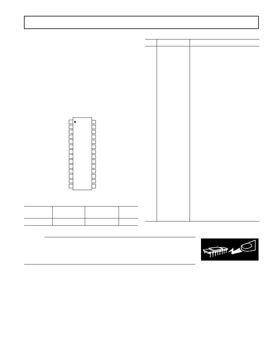
PIN CONFIGURATION
28
27
26
25
24
23
22
21
20
19
18
17
16
15
1
2
3
4
5
6
7
8
9
10
11
12
13
14
ADP3402
SIMGND
CLKIN
RESETIN
DATAIO
SIMBAT
CAP
VRTC
VBAT
VCC
PWRONKEY
ANALOGON
CHRON
ROWX
PWRONIN
I/O
RST
SIMPROG
SIMON
CLK
VSIM
CAP+
AGND
VCCA
REFOUT
RESET
RESCAP
DGND
VTCXO
PIN FUNCTION DESCRIPTIONS
Pin
Mnemonic
Function
1
VBAT
Battery Input Voltage
2
VCC
Digital Low Dropout Regulator
3
PWRONKEY
Power On/Off Key
4
ANALOGON
VTCXO Enable
5
PWRONIN
Power On/Off Signal from
Microprocessor
6
ROWX
Microprocessor Keyboard Output
7
CHRON
Charger On/Off Input
8
VRTC
Real-Time Clock Supply/Coin
Cell Battery Charger
9
CAP
Negative Side of Boost Capacitor
10
SIMBAT
Battery Input for the SIM
Charge Pump
11
DATAIO
Non-Level-Shifted Bidirectional
Data I/O
12
RESETIN
Non-Level-Shifted SIM Reset
13
CLKIN
Non-Level-Shifted Clock
14
SIMGND
Charge Pump Ground
15
I/O
Level-Shifted Bidirectional SIM
Data Input/Output
16
RST
Level-Shifted SIM Reset
17
SIMPROG
VSIM Programming:
Low = 3 V, High = 5 V
18
SIMON
VSIM Enable
19
CLK
Level-Shifted SIM Clock
20
VSIM
SIM Supply
21
CAP+
Positive Side of Boost Capacitor
22
RESCAP
Reset Delay Timing Cap
23
DGND
Digital Ground
24
VTCXO
Crystal Oscillator Low Dropout
Regulator
25
RESET
Main Reset
26
REFOUT
Reference Output
27
VCCA
Analog Low Dropout Regulator
28
AGND
Analog Ground
ORDERING GUIDE
Temperature
Package
Package
Model
Range
Description
Option
ADP3402ARU 20
°
C to +85
°
C
28-Lead TSSOP
RU-28A
ADP3402
6
REV. 0
Table I. LDO Control Logic
INPUTS
OUTPUTS
UVLO
CHRON
PWRONKEY
PWRONIN
ANALOGON
VRTC
VCC
VCCA
REFOUT
VTCXO
L
X
X
X
X
Off
Off
Off
Off
Off
H
H
X
X
X
On
On
On
On
On
H
X
L
X
X
On
On
On
On
On
H
L
H
L
X
On
Off
Off
Off
Off
H
L
H
H
L
On
On
On
On
Off
H
L
H
H
H
On
On
On
On
On
X = Don't care
Bold denotes the active control signal.
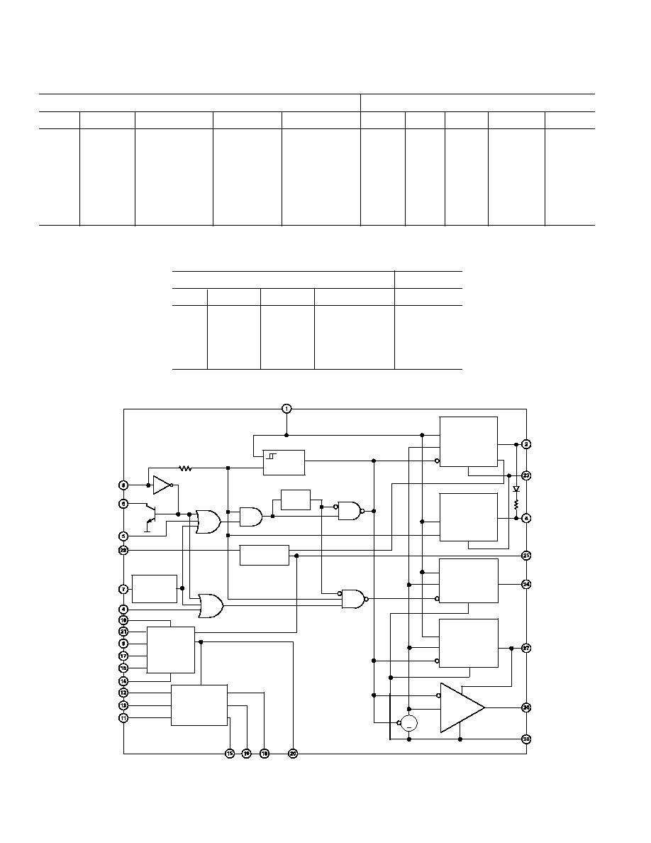
CHARGER
ON
THRESHOLD
OVER
TEMP
EN
REF
BUFFER
VBAT
VREF
EN
GND
PG
OUT
DIGITAL LDO
VCC
2.45V
DGND
VRTC
2.45V
VBAT
EN
GND
OUT
VBAT
VREF
EN
GND
OUT
POWER GOOD
RTC LDO
XTAL OSC LDO
ANALOG LDO
VBAT
VREF
EN
GND
OUT
REFOUT
AGND
VCCA
2.765V
VTCXO
2.765V
+
1.210V
UVLO
ADJ
UVLO
VBAT
PWRONKEY
ROWX
PWRONIN
RESCAP
RESET
CHRON
ANALOGON
SIMBAT
CAP+
CAP
SIMPROG
SIMON
SIMGND
RESETIN
CLKIN
DATAIO
CHARGE
PUMP
LOGIC
LEVEL
TRANSLATION
VSIM
RST
CLK
I/O
EN
3V/5V
20k
EN
ADP3402
RESET
GENERATOR
Figure 1. Functional Block Diagram
Table II. VSIM Control Logic
INPUTS
OUTPUTS
VCC
RESET
SIMON
SIMPROG
VSIM
Off
L
X
X
Off
On
L
X
X
Off
On
H
L
X
Off
On
H
H
L
3 V
On
H
H
H
5 V
X = Don't care
ADP3402
7
REV. 0
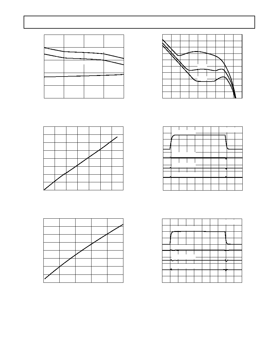
VBAT V
350
300
100
3
7
4
I
GND
A
5
6
250
200
150
PWRONIN, SIMON, AND ANALOGON
PWRONIN AND SIMON
PWRONIN
Figure 2. Ground Current vs. Battery Voltage
LOAD CURRENT mA
0
140
20
40
60
80
100
120
160
0
DROPOUT VOLTAGE mV
140
80
60
40
20
120
100
Figure 3. VCCA Dropout Voltage vs. Load Current
LOAD CURRENT mA
80
0
DROPOUT VOLTAGE mV
70
40
30
20
10
60
50
0
1
2
3
4
5
Figure 4. VTCXO Dropout Voltage vs. Load Current
VRTC V
200
0
0
2.7
0.3
I
RTC
A
0.6
0.9
1.2
1.5
1.8
2.1
2.4
180
100
60
40
20
160
140
80
120
+85 C
+25 C
20 C
Figure 5. RTC I/V Characteristic
VOLTAGE
TIME 100 s/DIV
VBAT 100 mV/DIV
3.2
3.0
MLCC CAPS
VCC 10 mV/DIV
VCCA 10 mV/DIV
VTCXO 10 mV/DIV
Figure 6. Line Transient Response, Maximum Loads
VOLTAGE
TIME 100 s/DIV
3.2
3.0
MLCC CAPS
VBAT (100 mV/DIV)
VCC (10 mV/DIV)
VCCA (10 mV/DIV)
VTCXO (10 mV/DIV)
Figure 7. Line Transient Response, Minimum Loads
ADP3402
8
REV. 0
VOLTAGE 20mV/DIV
TIME 200 s/DIV
I
LOAD
I = 100mA
MLCC CAPS
VCC
I = 200 A
Figure 8. VCC Load Step
VOLTAGE 20mV/DIV
TIME 100 s/DIV
I = 50 A
I
LOAD
I = 130mA
MLCC CAPS
VCCA
Figure 9. VCCA Load Step
VOLTAGE
TIME 50 s/DIV
PWRONIN AND ANALOGON (2V/DIV)
VCCA (100mV/DIV)
VTCXO (100mV/DIV)
VCC (100mV/DIV)
Figure 10. Turn-On Transients, Minimum Loads
VOLTAGE
TIME 50 s/DIV
PWRONIN AND ANALOGON (2V/DIV)
VCCA (100mV/DIV)
REFOUT (100mV/DIV)
VCC (100mV/DIV)
VTCXO (100mV/DIV)
Figure 11. Turn-On Transients, Maximum Loads
FREQUENCY Hz
80
70
0
4
100k
10
RIPPLE REJECTION dB
100
1k
10k
60
50
10
40
30
20
VTCXO
VCCA
VCC
REFOUT
MLCC OUTPUT CAPS
VBAT = 3.2V, FULL LOADS
Figure 12. Ripple Rejection vs. Frequency
VBAT V
80
0
2.5
3.3
2.6
RIPPLE REJECTION dB
2.7
2.8
2.9
3.0
3.1
3.2
70
40
30
20
10
60
50
FREQUENCY = 217Hz
MAX LOADS
VTCXO
VCCA
REFOUT
VCC
Figure 13. Ripple Rejection vs. Battery Voltage
ADP3402
9
REV. 0
ANALOG GND
DIGITAL AND
SIM GND
1
2
3
4
5
6
7
8
9
10
11
12
13
14
2.2 F
100nF
28
27
26
25
23
22
21
20
19
18
17
16
15
ADP3402
100
10 F
R1
CHARGER INPUT
R2
CAPACITOR-TYPE
BACKUP COIN CELL
10 F
SIM PIN OF
GSM PROCESSOR
2.2 F
10 F
24
0.22 F
100nF
10 F
CLK TO SIMCARD
RST TO SIMCARD
I/O TO SIM CARD
100nF
1 Li-ION OR
3 NiMH
CELLS
GSM
PROCESSOR
GSM
PROCESSOR
VBAT
VCC
PWRONKEY
ANALOGON
PWRONIN
ROWX
CHRON
VRTC
CAP
SIMBAT
DATAIO
RESETIN
CLKIN
SIMGND
AGND
VCCA
REFOUT
VTCXO
DGND
RESCAP
CAP+
VSIM
CLK
SIMON
SIMPROG
RST
I/O
RESET
Figure 15. Typical Application Circuit
FREQUENCY Hz
600
500
0
10
100k
100
VOLTAGE SPECTRAL NOISE DENSITY nV/ Hz
1k
10k
400
300
200
100
FULL LOAD
MLCC CAPS
VCCA
TCXO
REF
Figure 14. Output Noise Density
THEORY OF OPERATION
The ADP3402 is a power management chip optimized for use
with GSM baseband chipsets in handset applications. Figure 1
shows a block diagram of the ADP3402.
The ADP3402 contains several blocks:
· Four Low Dropout Regulators (Digital, Analog, Crystal
Oscillator, Real-Time Clock)
· Reset Generator
· Buffered Precision Reference
· SIM Interface Logic Level Translation (3 V/5 V)
· SIM Voltage Supply
· Power On/Off Logic
· Undervoltage Lockout
These functions have traditionally been done either as a discrete
implementation or as a custom ASIC design. ADP3402 combines
the benefits of both worlds by providing an integrated standard
product solution where every block is optimized to operate in a
GSM environment while maintaining a cost competitive solution.
Figure 15 shows the external circuitry associated with the ADP3402.
Only a few support components, mainly decoupling capacitors,
are required.
Input Voltage
The input voltage range for ADP3402 is 3 V to 7 V and optimized
for a single Li-Ion cell or three NiMH/NiCd cells. The ADP3402
uses Analog Devices' patented package thermal enhancement tech-
nology, which allows 15% improvement in power handling capabil-
ity over standard plastic packages. The thermal impedance (
JA
) of
the ADP3402 is 60
°
C/W. The charging voltage for a high capacity
NiMH cell can be as high as 5.5 V. Power dissipation should be
calculated at maximum ambient temperatures and battery voltage in
order not to exceed the 125
°
C maximum allowable junction tem-
perature. Figure 16 shows the maximum total LDO output current
as a function of ambient temperature and battery voltage.
However, high battery voltages normally occur only when the
battery is being charged and the handset is not in conversation
mode. In this mode there is a relatively light load on the LDOs.
A fully charged Li-Ion battery is 4.25 V, where the LDOs deliver
the maximum 240 mA up to the max 85
°
C ambient temperature.
ADP3402
10
REV. 0
AMBIENT TEMPERATURE C
300
0
20
0
TOTAL LDO CURRENT mA
20
40
60
80
250
200
150
100
50
85
VBAT = 5.5V
VBAT = 7V
VBAT = 6V
VBAT = 5V
4-LAYER BOARD
JA
= 60 C/W
Figure 16. Total LDO Load Current vs. Temperature and VBAT
Low Dropout Regulators (LDOs)
The ADP3402 high-performance LDOs are optimized for their
given functions by balancing quiescent current, dropout voltage,
line/load regulation, ripple rejection, and output noise. 2.2
µ
F
tantalum or MLCC ceramic capacitors are recommended for
use with the digital and analog LDOs, and 0.22
µ
F for the
TCXO LDO.
Digital LDO (VCC)
The digital LDO (VCC) supplies all the digital circuitry in the
handset (baseband processor, baseband converter, external
memory, display, etc). The LDO has been optimized for very
low quiescent current (30
µ
A maximum) at light loads as this
LDO is on at all times.
Analog LDO (VCCA)
This LDO has the same features as the digital LDO. It has further-
more been optimized for good low frequency ripple rejection for use
with analog sections in order to reject the ripple coming from the RF
power amplifier. VCCA is rated to 130 mA load which is sufficient
to supply the complete analog section of a baseband converter such
as the AD6421/AD6425, including a 32
earpiece.
TCXO LDO (VTCXO)
The TCXO LDO is intended as a supply for temperature com-
pensated crystal oscillator, which needs its own ultralow noise
supply. The output current is rated to 5 mA for the TCXO LDO.
RTC LDO (VRTC)
The RTC LDO charges a capacitor-type backup coin cell to run
the real-time clock module. It has been targeted to charge elec-
tric double layer capacitors such as the PAS621 from Kanebo.
The PAS621 has a small physical size (6.8 mm diameter) and a
nominal capacity of 0.3 F, giving many hours of backup time.
ADP3402
GSM PROCESSOR
VRTC
PWRON
PWRONIN
COIN
CELL
VRTC
RTC
MODULE
Figure 17. Connecting VRTC and POWERONIN to the Chipset
The ADP3402 supplies current both for charging the coin cell and
for the RTC module when the digital supply is off. The nominal
charging voltage is 2.45 V, which ensures long cell life while obtain-
ing in excess of 90% of the nominal capacity. In addition, it features
a very low quiescent current (10
µ
A) since this LDO is running all
the time, even when the handset is switched off. It also has reverse
current protection with low leakage which is needed when the main
battery is removed and the coin cell supplies the RTC module.
Reference Output (REFOUT)
The reference output is a low noise, high precision reference with a
guaranteed accuracy of 1.5% over temperature. The reference can
be fed to the baseband converter, such as the AD6425, improving
the absolute accuracy of the converters from 5% to 1.5%. This
significantly reduces calibration time needed for the baseband
converter during production.
SIM Interface
The SIM interface generates the needed SIM voltage--either 3 V
or 5 V, dependent on SIM type, and also performs the needed
logic level translation. Quiescent current is low, as the SIM card
will be powered all the time. Note that DATAIO and I/O have
integrated pull-up resistors as shown in Figure 18. See Table II for
the control logic of the charge pump output, VSIM.
RESETIN
CLKIN
DATAIO
RST
CLK
I/O
LEVEL
SHIFT
VCC
VSIM
ADP3402
LEVEL
SHIFT
VCC
VCC
VSIM
VSIM
Figure 18. Schematic for Level Translators
Power-On/-Off
ADP3402 handles all issues regarding power-on/-off of the hand-
set. It is possible to turn on the ADP3402 in three different ways:
· Pulling PWRONKEY Low
· Pulling PWRONIN High
· CHRON exceeds threshold
Pulling PWRONKEY key low is the normal way of turning on the
handset. This will turn on all the LDOs as long as PWRONKEY is
held low. The microprocessor then starts and pulls PWRONIN
high after which PWRONKEY can be released. PWRONIN going
high will also turn on the handset. This is the case when the alarm
in the RTC module expires.
An external charger can also turn on the phone. The turn-on
threshold and hysteresis can be programmed via external resistors
to allow full flexibility with any external charger and battery chem-
istry. These resistors are referred to as R1 and R2 in Figure 15.
Undervoltage Lockout (ULVO)
The UVLO function in the ADP3402 prevents startup when the
initial voltage of the main battery is below the 3.2 V threshold.
If the battery is this low with no load, there will be little or no
capacity left. When the battery is greater than 3.2 V, as with the
insertion of a fresh battery, the UVLO comparator trips, the

ADP3402
11
REV. 0
RTC LDO is enabled, and the threshold is reduced to 3.0 V.
This allows the handset to start normally until the battery volt-
age decays to 3.0 V open circuit. Once the 3.2 V threshold is
exceeded, the RTC LDO is enabled. If, however, if the backup
coin cell is not connected, or is damaged or discharged below
1.5 V, the RTC LDO will not start on its own. In this situation,
the RTC LDO will be started by enabling the VCC LDO.
Once the system is started, i.e., the phone is turned on and the
VCC LDO is up and running, the UVLO function is entirely
disabled. The ADP3402 is then allowed to run down to very low
battery voltages, typically around 2 V. The battery voltage is
normally monitored by the microprocessor and usually shuts the
phone off at around 3.0 V.
If the phone is off, i.e., the VCC LDO is off, and the battery
voltage drops below 3.0 V, the UVLO circuit disables startup
and the RTC LDO. This is implemented with very low quies-
cent current, typically 3
µ
A, to protect the main battery against
any damage. NiMH batteries can reverse polarity if the 3-cell
battery voltage drops below 3.0 V and a current of more than
about 40
µ
A continues to flow. Lithium ion batteries will lose
their capacity, although the built-in safety circuits normally
present in these cells will most likely prevent any damage.
RESET
ADP3402 contains reset circuitry that is active both at power-up
and at power-down. RESET is held low at power-up. An inter-
nal power-good signal starts the reset delay. The delay is set by
an external capacitor on RESCAP:
t
C
RESET
RESCAP
=
×
1 0
. ms/nF
A 100 nF capacitor will produce a 100 ms reset time. At power-
off, RESET will be kept low to prevent any spurious microproces-
sor starts. The current capability of RESET is low (a few hundred
nA) when VCC is off, to minimize power consumption. There-
fore, RESET should only be used to drive a single CMOS input.
When VCC is on, RESET will drive about 15
µ
A.
Overtemperature Protection
The maximum die temperature for ADP3402 is 125
°
C. If the die
temperature exceeds 160
°
C, the ADP3402 will disable all the LDOs
except the RTC LDO, which has very limited current capabilities.
The LDOs will not be re-enabled before the die temperature is
below 125
°
C, regardless of the state of PWRONKEY, PWRONIN,
and CHRON. This ensures that the handset will always power-off
before the ADP3402 exceeds its absolute maximum thermal ratings.
APPLICATIONS INFORMATION
Input Capacitor Selection
For the input voltage, VBAT, of the ADP3402, a local bypass
capacitor is recommended. Use a 5
µ
F to 10
µ
F, low ESR capaci-
tor. Multilayer ceramic chip capacitors provide the best combina-
tion of low ESR and small size, but may not be cost effective. A
lower cost alternative may be to use a 5
µ
F to 10
µ
F tantalum
capacitor with a small (1
µ
F to 2
µ
F) ceramic in parallel.
LDO Capacitor Selection
The performance of any LDO is a function of the output capaci-
tor. The digital and analog LDOs require a 2.2
µ
F capacitor and
the TCXO LDO requires a 0.22
µ
F capacitor. Larger values
may be used, but the overshoot at startup will increase slightly.
If a larger output capacitor is desired, be sure to check that the
overshoot and settling time are acceptable for the application.
All the LDOs are stable with a wide range of capacitor types and
ESR due to Analog Devices' anyCAP technology. The ADP3402
is stable with extremely low ESR capacitors (ESR ~ 0), such as
multilayer ceramic capacitors, but care should be taken in their
selection. Note that the capacitance of some capacitor types show
wide variations over temperature or with dc voltage. A good quality
dielectric, X7R or better, is recommended.
The RTC LDO has a rechargeable coin cell or an electric double-
layer capacitor as a load, but a 0.1
µ
F ceramic capacitor is recom-
mended for stability and best performance.
Charge Pump Capacitor Selection
For the input (SIMBAT) and output (VSIM) of the SIM charge
pump, use 10
µ
F low ESR capacitors. The use of low ESR capaci-
tors improves the noise and efficiency of the SIM charge pump.
Multilayer ceramic chip capacitors provide the best combination of
low ESR and small size but may not be cost effective. A lower cost
alternative may be to use a 10
µ
F tantalum capacitor with a small
(1
µ
F to 2
µ
F) ceramic capacitor in parallel.
For the lowest ripple and best efficiency, use a 0.1
µ
F, ceramic
capacitor for the charge pump flying capacitor (CAP+ and CAP).
A good quality dielectric, such as X7R is recommended.
Setting the Charger Turn-On Threshold
The ADP3402 can be turned on when the charger input exceeds
a programmable threshold voltage. The charger's threshold and
hysteresis are set by selecting the values for R1 and R2 shown in
Figure 15.
The turn-on threshold for the charger is calculated using:
V
R
R
R
R
R
V
CHR
HYS
HYS
T
=
+
×
×
+
×
2
2
1
1
Where V
T
is the CHRON threshold voltage and R
HYS
is the
CHRON hysteresis resistance.
The hysteresis is determined using:
V
V
R
R
HYS
T
HYS
=
×
1
Combining the above equations and solving for R1 and R2 gives
the following formulas:
R
R
V
V
HYS
T
HYS
1
=
×
R
R
R
V
V
R
R
HYS
CHR
T
HYS
2
1
1
1
=
×
-
×
-
Example: R1 = 10 k
and R2 = 30.2 k
gives a charger thresh-
old (not counting the drop in the power Schottky diode) of
3.5 V
±
160 mV with a 200 mV
±
30 mV hysteresis.
Charger Diode Selection
The diode shown in Figure 15 is used to prevent the battery from
discharging into the charger turn-on setting resistors, R1 and R2. A
Schottky diode is recommended to minimize the voltage difference
from the charger to the battery and the power dissipation. Choose
a diode with a current rating high enough to handle both the bat-
tery charging current and the current the ADP3402 will draw if
powered up during charging. The battery charging current is de-
pendent on the battery chemistry, and the charger circuit. The
ADP3402 current will be dependent on the loading.
12
REV. 0
C376281/00 (rev. 0)
PRINTED IN U.S.A.
ADP3402
Printed Circuit Board Layout Considerations
Use the following general guidelines when designing printed
circuit boards:
1. Split the battery connection to the VBAT and SIMBAT pins
of the ADP3402. Use separate traces for each connection
and locate the input capacitors as close to the pins as possible.
2. SIM input and output capacitors should be returned to the
SIMGND and kept as close as possible to the ADP3402 to
minimize noise. Traces to the SIM charge pump capacitor
should be kept as short as possible to minimize noise.
3. VCCA and VTCXO capacitors should be returned to
AGND.
4. VCC and VRTC capacitors should be returned to DGND.
5. Split the ground connections. Use separate traces or planes for
the analog, digital, and power grounds, and tie them together
at a single point, preferably close to the battery return.
OUTLINE DIMENSIONS
Dimensions shown in inches and (mm).
28-Lead Thin Shrink Small Outline (TSSOP)
(RU-28A)
0.244 (6.20)
0.236 (6.00)
28
15
14
1
0.386 (9.80)
0.378 (9.60)
0.325 (8.25)
0.313 (7.95)
PIN 1
SEATING
PLANE
0.006 (0.15)
0.002 (0.05)
0.0118 (0.30)
0.0075 (0.19)
0.0256
(0.65)
BSC
0.0433 (1.10)
MAX
0.0374 (0.95)
0.0335 (0.85)
0.0078 (0.200)
0.0035 (0.090)
0.030 (0.75)
0.020 (0.50)
8
0