 | –≠–ª–µ–∫—Ç—Ä–æ–Ω–Ω—ã–π –∫–æ–º–ø–æ–Ω–µ–Ω—Ç: ADP3206 | –°–∫–∞—á–∞—Ç—å:  PDF PDF  ZIP ZIP |
Document Outline
- FEATURES
- APPLICATIONS
- GENERAL DESCRIPTION
- FUNCTIONAL BLOCK DIAGRAM
- ˛ˇ
- ˛ˇ
- ˛ˇ
- ˛ˇ
- ˛ˇ
- ˛ˇ
- ˛ˇ
- ˛ˇ
- ˛ˇ

2-/3-/4-Phase Synchronous Buck
Controller for IMVP-5 CPUs
ADP3206
Rev. 0
Information furnished by Analog Devices is believed to be accurate and reliable.
However, no responsibility is assumed by Analog Devices for its use, nor for any
infringements of patents or other rights of third parties that may result from its use.
Specifications subject to change without notice. No license is granted by implication
or otherwise under any patent or patent rights of Analog Devices. Trademarks and
registered trademarks are the property of their respective owners.
One Technology Way, P.O. Box 9106, Norwood, MA 02062-9106, U.S.A.
Tel: 781.329.4700
www.analog.com
Fax: 781.326.8703
© 2004 Analog Devices, Inc. All rights reserved.
FEATURES
Selectable 2-, 3-, or 4-phase operation at up to
1 MHz per phase
6-bit digitally programmable 0.8375 V to 1.6 V output
±10 mV DAC accuracy over temperature
Logic-level PWM outputs for interface to
external high power drivers
Active current/thermal balancing between phases
Built-in power good/crowbar blanking supports
on-the-fly VID code changes
Programmable deep sleep offset and deeper sleep
reference voltage
Programmable soft transient control to minimize
inrush currents during output voltage changes
Programmable short circuit protection with
programmable latch-off delay
APPLICATIONS
Desk-note and notebook PC power supplies for IMVP-5
compliant IntelÆ processors
GENERAL DESCRIPTION
The ADP3206 is a highly efficient multiphase synchronous
buck-switching regulator controller optimized for converting
the notebook main supply into the core supply voltage required
by IMVP-5 Intel processors. It uses an internal 6-bit DAC to
read a voltage identification (VID) code directly from the
processor, which is used to set the output voltage between
0.8375 V and 1.6 V, and uses a multimode PWM architecture
to drive the logic-level outputs at a programmable switching
frequency that can be optimized for VR size and efficiency. The
phase relationship of the output signals can be programmed to
provide 2-, 3-, or 4-phase operation.
The ADP3206 includes programmable no-load offset and slope
functions to adjust the output voltage as a function of the load
current so that it is always optimally positioned for a system
transient. The ADP3206 also provides accurate and reliable
short circuit protection, adjustable current limiting, deep sleep
and deeper sleep programming inputs, and a delayed power
good output that accommodates on-the-fly output voltage
changes requested by the CPU.
ADP3206 is specified over the commercial temperature range of
0∞C to 100∞C and is available in a 40-lead LFCSP package.
FUNCTIONAL BLOCK DIAGRAM
DPSLP
SD
12
24
22
21
13
35
16
15
23
14
17
4
2
7
40
39
38
37
36
1
6
30
29
5
8
9
10
11
3
20
18
19
25
26
27
28
31
32
33
34
OD2
OD1
SOFT
START
DELAY
THERMAL
THROTTLING
CONTROL
OSCILLATOR
GND
VCC
RAMPADJ RT
ADP3206
DELAY
PWRGD
ILIMIT
TTMASK
TTSENSE
VRTT
PWM2
FB
DPRSLP
DPSET
DPRSET
PGMASK
STSET
04651-0-001
PWM3
PWM4
SW1
CSSUM
CSCOMP
SW2
SW3
SW4
CSREF
PWM1
VID0 VID1 VID2 VID3
VID5
VID4
FBRTN REF
COMP
CSREF
CURRENT-
LIMITING
CIRCUIT
CROWBAR
CURRENT LIMIT
CURRENT-
BALANCING
CIRCUIT
2-/3-/4-PHASE
DRIVER LOGIC
EN
SET
RESET
RESET
RESET
RESET
DEEP/
DEEPER
SLEEP
CONTROL
PRECISION
REFERENCE
UVLO
SHUTDOWN
AND BIAS
CMP
CMP
CMP
CMP
VID
DAC
Figure 1.

ADP3206
Rev. 0| Page 2 of 32
TABLE OF CONTENTS
Specifications..................................................................................... 3
Test Circuits....................................................................................... 6
Absolute Maximum Ratings............................................................ 7
Pin Configuration and Function Descriptions............................. 8
Typical Performance Characteristics ........................................... 10
Theory of Operation ...................................................................... 11
Number of Phases ...................................................................... 11
Master Clock Frequency............................................................ 11
Output Voltage Differential Sensing ........................................ 11
Output Current Sensing ............................................................ 11
Active Impedance Control Mode............................................. 12
Current Control Mode and Thermal Balance ........................ 12
Voltage Control Mode................................................................ 12
Deep Sleep and Deeper Sleep Settings..................................... 13
Soft-Start...................................................................................... 14
Current Limit, Short Circuit, and Latch-Off Protection ....... 14
Dynamic VID.............................................................................. 15
Power Good Monitoring ........................................................... 15
Output Crowbar ......................................................................... 15
Output Enable and UVLO ........................................................ 15
Thermal Throttling Control...................................................... 15
Application Information................................................................ 18
Setting the Clock Frequency ..................................................... 18
Soft-Start, Power Good, and Current Limit Latch-Off
Delay Times................................................................................. 18
Inductor Selection ...................................................................... 18
Selecting a Standard Inductor................................................... 19
Output Droop Resistance.......................................................... 19
Inductor DCR Temperature Correction ................................. 20
Output Offset .............................................................................. 20
C
OUT
Selection ............................................................................. 21
Power MOSFETS........................................................................ 21
Ramp Resistor Selection............................................................ 22
COMP Pin Ramp ....................................................................... 22
Current Limit SetPoint .............................................................. 22
Feedback Loop Compensation Design.................................... 23
C
IN
Selection and Input Current di/dt Reduction.................. 23
Deepersleep Voltage and Transient Setting............................. 24
Deepsleep Offset Voltage Setting ............................................. 25
PWRGD Mask Timer Setting ................................................... 25
Selecting Thermal Monitor Components ............................... 25
Tuning Procedure for ADP3206............................................... 26
Layout and Component Placement ............................................. 28
General Recommendations....................................................... 28
Power Circuitry .......................................................................... 28
Signal Circuitry........................................................................... 28
Outline Dimensions ....................................................................... 29
Ordering Guide .......................................................................... 30
REVISION HISTORY
4/04--Revision 0: Initial Version

ADP3206
Rev. 0| Page 3 of 32
SPECIFICATIONS
Table 1. VCC = 5 V, FBRTN = DPRSLP = GND, SD = 1.2 V, DPSLP = 3.3 V, T
A
= 0
o
C to 100
o
C, unless otherwise noted.
1
Parameter Symbol
Conditions Min
Typ
Max
Unit
REFERENCE and VID DAC
Reference Output Voltage
V
REF
I
REF
= 100
µA
2.95 3.0
3.05 V
I
REF
= 4 mA
2.93
3.0
3.07
V
Output Current Range
I
REF
0
4
mA
Normal Mode Output Accuracy
V
FB
Relative to nominal DAC output,
referenced to FBRTN, DPRSLP = 0 V
-10
+10
mV
Deeper Sleep Output Accuracy
V
STSET
Relative to DPRSET input, referenced
to FBRTN, DPRSLP = 3.3 V
-5
+5
mV
Input Low Voltage
V
IL(VID)
0.4
V
Input High Voltage
V
IH(VID)
0.8
V
Input Current, Input Voltage Low
I
IL(VID)
VID(X) = 0 V
-20
-30
µA
Input Current, Input Voltage High
I
IH(VID)
VID(X) = 1.25 V
5
15
µA
Pull-up resistance
R
VID
35
60
k
Internal Pull-up Voltage
0.9
1.1
1.25
V
VID Transition Delay Time
1
VID change to DACREF change
400
ns
No CPU Detection Turn-off Delay
Time
2
VID change to 1111 to PWM going
low
400
ns
DEEPSLEEP/DEEPERSLEEP
CONTROL
DPSLP,
DPRSLP
Input Low Voltage
V
IL
0.8
V
Input High Voltage
V
IH
2.0
V
Input Current
-1
1
µA
OD1,
OD2
Output Voltage Low
V
OL
I
ODX
(SINK)
= 400
µA
80 500
mV
Output Voltage High
V
OH
I
ODX
(SOURCE)
= 400
µA
4.0 5.0
V
DPSET
Output Voltage
V
DPSET
DPSET ≠ Nominal VID output
-70
+70
mV
Output Current Range
I
DPSET
0
100
µA
DPRSET
Input Voltage Range
V
DPRSET
0.5
1.0
V
Input Current
I
DPRSET
-1
1
µA
STSET
Minimum Capacitance
C
STET
100
pF
Transient Time
DPSET = 0.75 V
100
µs
Nominal VID output = 1.55 V,
C
STSET
= 1.5 nF
Output Voltage Range
0.5
3
V
Output Current
I
STSET
DPSET = 0.75 V, DPRSLP ≠ 3.3 V
V
STSET
= 2 V
-19
-16
-13
µA
V
STSET
= 0.5 V
13
16
19
µA
THERMAL
THROTTLING
CONTROL
TTSENSE Voltage Range
0
2
V
TTSENSE Threshold Voltage
1.46
1.5
1.54
V
TTSENSE Bias Current
-1
1
µA
TTMASK Threshold Voltage
1.45
1.5
1.55
V
TTMASK Output Low Voltage
TTSENSE static, I
TTMASK(SINK)
= 1 mA
200
mV
VRTT Output Voltage Low
V
OL
I
VRTT(SINK)
= 200
µA
100 500 mV
VRTT Output Voltage High
V
OH
I
VRTT(SOURCE)
= 200
µA
4.0 5.0
V

ADP3206
Rev. 0| Page 4 of 32
Parameter Symbol
Conditions Min
Typ
Max
Unit
ERROR
AMPLIFIER
Output Voltage Range
V
COMP
0.8
3.3
V
Line Regulation
V
FB
VCC = 4.5 V to 5.5 V
0.05
%
FB Input Bias Current
I
FB
DPSLP = 3.3 V
14
16
18
µA
DPSLP = DRSLP = 0 V, I
DPSET
= 60
µA
70 75 80
µA
FBRTN Current
I
FBRTN
85
120
µA
Output Current
I
O(ERR)
FB Forced to V
OUT
= 3%
500
µA
Gain Bandwidth Product
GBW
(ERR)
COMP = FB
20
MHz
Slew Rate
C
COMP
= 10 pF
50
V/
µs
OSCILLATOR
Frequency Range
2
f
OSC
0.25
4
MHz
Frequency Variation
f
PHASE
T
A
= +25
∞
C, R
T
= 250 k
, 4-Phase
155
200 245 kHz
T
A
= +25
∞
C, R
T
= 115 k
, 4-Phase
400
kHz
T
A
= +25
∞
C, R
T
= 75 k
, 4-Phase
600
kHz
Output Voltage
VRT
R
T
= 100 k
to GND
1.9
2.0 2.1 V
RAMPADJ Output Voltage
V
RAMPADJ
RAMPADJ = FB
-50
+50
mV
RAMPADJ Input Current Range
I
RAMPADJ
100
µA
CURRENT SENSE AMPLIFIER
Offset Voltage
V
OS(CSA)
CSSUM ≠ CSREF, see Figure 1
-1.5
+1.5
mV
Gain Bandwidth Product
GBW(
CSA)
10
MHz
Slew Rate
C
CSCOMP
= 10 pF
25
V/
µs
Input Common Mode Range
CSSUM and CSREF
0
3
V
Positioning Accuracy
V
FB
FB ≠ V
VID
, see Figure 2
-75
-80
-85
mV
CSSUM Bias Current
I
CSSUM
20
100
nA
CSREF Bias Current
I
CSREF
0.5
5
µA
Output Current
2
I
CSCOMP
CSAMP unity gain
Sourcing
500
µA
Sinking
-300
µA
CURRENT BALANCE CIRCUIT
Common Mode Range
V
SW(X)CM
-600
+200
mV
Input Resistant
R
SW(X)
S
W(X)
= 0 V
22
32
42
k
Input Current
I
SW(X)
S
W(X)
= 0 V
4
7
10
µA
Input Current Matching
I
SW(X)
S
W(X)
= 0 V
-5
+5
%
CURRENT
LIMIT
COMPARATOR
Output Voltage
V
ILIMIT
R
ILIMIT
= 200 k
0.95 1
1.05 V
Output Current
I
ILIMIT
R
ILIMIT
= 200 k
5
µA
Current Limit Threshold Voltage
V
CL
V
CSREF
≠ V
CSCOMP
, R
ILIMIT
= 200 k
4 Phase
DPRSLP = 0 V
105
120
145
mV
DPRSLP = 3.3 V
15
30
45
mV
Latch-Off Delay Threshold
V
DELAY
In current limit
1.7
1.8
1.9
V
Latch-Off Delay Time
t
DELAY
R
DELAY
= 250 k
C
DELAY
= 4.7 nF
1.2
ms
SOFT
START
Output Current, Soft-Start Mode
I
DELAY(SS)
During start-up, delay < 2.8 V
15
20
25
µA
Output Voltage
V
DELAY
3
V
Soft-Start Delay Time
t
DELAY(SS)
R
DELAY
= 250 k
, C
DELAY
= 4.7 nF,
VID code = 011111
600
µs

ADP3206
Rev. 0| Page 5 of 32
Parameter Symbol
Conditions Min
Typ
Max
Unit
SHUTDOWN
INPUT
Input Low Voltage
V
IL(
SD
)
0.4
V
Input High Voltage
V
IH(
SD
)
0.8
V
Input Current, Input Voltage Low
I
IL(
SD
)
SD = 0 V
-1
1
µA
Input Current, Input Voltage High
I
IH(
SD
)
SD = 1.25 V
10 25
µA
POWER GOOD COMPARATOR
Undervoltage Threshold
V
PWRGD(UV)
Relative to nominal output
-200
-250
-300
mV
Overvoltage Threshold
V
PWRGD(OV)
Relative to nominal output
100
150
200
mV
Output Low Voltage
V
OL(PWRGD)
I
PWRGD(SINK)
= 4 mA
150
400
mV
Power Good Delay Time
VID Code Changing
C
PGMASK
= 150 pF
90
µs
VID Code Static
200
ns
Crowbar Trip Point
V
CROWBAR
Relative to nominal output
100
150
200
mV
Crowbar Reset Point
350
450
550
mV
Crowbar Delay Time
t
CROWBAR
Overvoltage to PWM going low
VID Code Changing
C
PGMASK
= 150 pF
90
µs
VID Code Static
400
ns
POWER GOOD MASKING
Threshold Voltage
2.85
3
3.15
V
Output Current
DPRSLP or VID changing,
3.5
5
6.5
µA
V
PGMASK
= 0 V
DPRSLP or VID static,
500
µA
V
PGMASK
= 0.5 V
PWM
OUTPUTS
Output Voltage Low
V
OL(PWM)
I
PWM(SINK)
= 400
µA
100 500 mV
Output Voltage High
V
OH(PWM)
I
PWM(SOURCE)
= 400
µA
4.0
5.0
V
SUPPLY
Supply Voltage Range
V
CC
4.5
5.5
V
Supply Current
I
CC
3.5 6 mA
UVLO Threshold Voltage
V
UVLO
VCC
Rising
3.6
3.8 4.1 V
UVLO Hysteresis
V
UVLO
50
100 150 mV
1
All limits at temperature extremes are guaranteed via correlation using Standard Statistical Quality Control (SQC).
2
Guaranteed by design or bench characterization, not production tested.

ADP3206
Rev. 0| Page 6 of 32
TEST CIRCUITS
250k
5V
1.25V
1
µ
F
+
100nF
100nF
6-BIT CODE
250k
20k
1k
4.7nF
ADP3206
TOP VIEW
PIN 1
INDICATOR
1
2
3
4
5
6
7
8
9
10
30
29
28
27
26
25
24
23
22
21
40
39
38
37
36
35
34
33
32
31
11
12
13
14
15
16
17
18
19
20
04651-0-002
Figure 2. Closed-Loop Output Voltage Accuracy
+
≠
CSSUM
20
CSCOMP
19
35
VCC
CSREF
18
GND
21
39k
100nF
1k
1.0V
ADP3206
5V
V
OS
=
CSCOMP ≠ 1V
40
04651-0-003
Figure 3. Current Sense Amplifier V
OS
+
≠
CSSUM
20
CSCOMP
19
35
VCC
CSREF
18
COMP
3
FB
4
GND
21
200k
10k
200k
1.0V
ADP3206
V
5V
100nF
V
FB
= FB
V = 80mV
≠ FB
V = 0mV
04651-0-004
Figure 4. Positioning Voltage

ADP3206
Rev. 0| Page 7 of 32
ABSOLUTE MAXIMUM RATINGS
Table 2.
Parameter Rating
VCC
≠0.3 V to + 6 V
FBRTN
≠0.3 V to + 0.3 V
SW1 ≠ SW4
≠5 V to + 25 V
All other Inputs & Outputs
≠0.3 V to + 6 V
Operating Ambient Temperature
Range
0∞C to +100∞C
Operating Junction Temperature
125∞C
Storage Temperature Range
≠65∞C to +150∞C
JA
100∞C/W
Lead Temperature Range
(Soldering 10 sec)
300∞C
Infrared (15 sec)
260∞C
Stresses above those listed under Absolute Maximum Ratings
may cause permanent damage to the device. This is a stress
rating only; functional operation of the device at these or any
other conditions above those indicated in the operational
section of this specification is not implied. Exposure to absolute
maximum rating conditions for extended periods may affect
device reliability. Absolute maximum ratings apply individually
only, not in combination. Unless otherwise specified all other
voltages are referenced to GND.
ESD CAUTION
ESD (electrostatic discharge) sensitive device. Electrostatic charges as high as 4000 V readily accumulate on
the human body and test equipment and can discharge without detection. Although this product features
proprietary ESD protection circuitry, permanent damage may occur on devices subjected to high energy
electrostatic discharges. Therefore, proper ESD precautions are recommended to avoid performance
degradation or loss of functionality.

ADP3206
Rev. 0| Page 8 of 32
PIN CONFIGURATION AND FUNCTION DESCRIPTIONS
PIN
INDICATOR
TOP VIEW
04651-0-005
28 SW1
27 SW2
26 SW3
25 SW4
24 VRTT
23 TTSENSE
22 TTMASK
21 GND
FBRTN 2
FB 3
COMP 4
PGMASK 5
STSET 6
REF 7
DPRSET 8
DPSET 10
DPRSLP 9
VID5 1
37 VID
3
P
W
RGD 1
2
DE
LAY
1
4
CS
RE
F 1
8
C
SSU
M
19
CS
COMP
2
0
RT 1
5
D
PSSLP 11
SD
13
36 VID
4
35 VC
C
34 PW
M
1
39 VID
1
33 PW
M
2
32 PW
M
3
31 PW
M
4
ADP3206
RAMP
ADJ
1
6
ILIMIT 17
29 OD2
30 OD1
38 VID
2
40 VID
0
Figure 5. Pin Configuration
Table 3. Pin Function Descriptions
Pin No.
Mnemonic
Description
1, 36 to 40
VID5, VID4 to
VID0
Voltage Identification DAC Inputs. These six pins are pulled up to an internal reference, providing a Logic 1 if
left open. When in normal operation mode, the DAC output programs the FB regulation voltage from 0.8375
V to 1.6 V. Leaving all VID4 through VID0 open results in the ADP3206 going into a "No CPU" mode, shutting
off its PWM outputs.
2
FBRTN
Feedback Return. VID DAC and error amplifier reference for remote sensing of the output voltage.
3 FB Feedback Input. Error amplifier input for remote sensing of the output voltage. An external resistor between
this pin and the output voltage sets the no-load offset point.
4 COMP
Error
Amplifier
Output and Compensation Point.
5 PGMASK
Power Good Masking. A capacitor connected between this pin and GND sets the Power Good Comparator
masking time during DPRSLP and VID pin transitions.
6 STSET
Soft Transient Setting Input. A capacitor connected between this pin and GND controls the slew rate of the
output voltage during transitions between various operating modes.
7
REF
Internal 3 V Reference Output.
8
DPRSET
Deeper Sleep Voltage Setting Input used as the DAC reference voltage when DPRSLP is asserted.
9
DPRSLP
Deeper Sleep Control Input.
10 DPSET Deep Sleep Offset Voltage Setting Input. The offset programmed by a resistor connected between this pin
and GND is activated when DPSLP is asserted.
11
DPSLP
Deep Sleep Control Input.
12 PWRGD
Power Good Output. Open drain output that signals when the output voltage is outside of the proper
operating range.
13
SD
Power Supply Enable Input. Pulling this pin to GND disables the PWM outputs.
14 DELAY Soft-start Delay and Current Limit Latch-off Delay Setting Input. An external resistor/capacitor connected
between this pin and GND sets the soft-start ramp-up time and the overcurrent latch-off delay time.
15 RT
Frequency Setting Resistor Input. An external resistor connected between this pin and GND sets the oscillator
frequency of the device.
16 RAMPADJ
PWM Ramp Current Input. An external resistor from the converter input voltage to this pin sets the internal
PWM ramp.
17 ILIMIT Current Limit Set Point. An external resistor from this pin to GND sets the current limit threshold of the
converter.
18 CSREF Current Sense Reference Voltage Input. The voltage on this pin is used as the reference for the current sense
amplifier and the power good and crowbar functions. This pin should be connected to the common point of
the output inductors.
19 CSSUM
Current Sense Summing Node. External resistors from each switch node to this pin sum the average inductor
currents together to measure the total output current.

ADP3206
Rev. 0| Page 9 of 32
Pin No.
Mnemonic
Description
20 CSCOMP
Current Sense Compensation Point. A resistor and capacitor from this pin to CSSUM determines the slope of
the load line and the positioning loop response time.
21
GND
Ground. All internal biasing and the logic output signals of the device are referenced to this ground.
22 TTMASK
Thermal Throttling Masking Time Setting Input. An external resistor from this pin to VCC and an external
capacitor to GND set the delay time during which the VRTT output is masked. This delay is triggered by the
assertion or de-assertion of VRTT.
23 TTSENSE
VR Hot Thermal Throttling Sense Input. This pin monitors the common tap point of an external resistor-
thermistor voltage divider network and causes VRTT output signal to go high if the remotely sensed hot spot
temperature exceeds the programmed temperature threshold.
24 VRTT Voltage Regulator Thermal Throttling Output. This logic output alerts the CPU that the temperature at one of
the designated monitoring points has exceeded the programmed temperature threshold.
25-28
SW4 ≠ SW1
Current Balance Inputs. Inputs for measuring the current level in each phase. The SW pins of unused phases
should be left open.
29
OD2
This pin is actively pulled low under the same conditions as those of OD1. In addition, this pin is actively
pulled low when DPRSLP is asserted. This pin is normally connected to the SD input of the drivers for phases
2 through 4.
30
OD1
This pin is actively pulled low when the ADP3206 SD input is low, or when VCC is below its UVLO threshold
to signal to the driver IC that the driver high-side and low-side outputs should go low. This pin is normally
connected to the SD input of the phase 1 driver.
31-34 PWM4
≠
PWM1
Logic-level PWM Outputs. Each output connects to the input of an external MOSFET driver. Connecting the
PWM3 and/or PWM4 outputs to GND causes that phase to turn off, allowing the ADP3206 to operate as a
2-, 3-, or 4-phase controller.
35
VCC
Supply Voltage for the device.

ADP3206
Rev. 0| Page 10 of 32
TYPICAL PERFORMANCE CHARACTERISTICS
4
3
2
1
0
MASTER CLOCK FREQUENCY (MHz)
R
T
VALUE (k
)
0
50
100
150
200
250
300
04651-0-006
Figure 6. Master Clock Frequency vs. R
T
0
0.5
1.0
1.5
2.0
2.5
3.0
3.5
4.0
3.9
3.8
3.7
3.6
3.5
3.4
3.3
3.2
S
U
P
P
L
Y
CURRE
NT (mA)
MASTER CLOCK FREQUENCY (MHz)
TA = 25∞C
4-PHASE OPERATION
04651-0-007
Figure 7. Supply Current vs. Oscillator Frequency

ADP3206
Rev. 0| Page 11 of 32
THEORY OF OPERATION
The ADP3206 combines a multimode, fixed frequency PWM
control with multiphase logic outputs for use in 2-, 3-, and
4-phase synchronous buck CPU core supply power converters.
The internal 6-bit VID DAC conforms to Intel's IMVP-5
specifications. Multiphase operation is important for producing
the high currents and low voltages demanded by today's
microprocessors. Handling the high currents in a single-phase
converter would place high thermal demands on the
components in the system such as the inductors and MOSFETs.
The multimode control of the ADP3206 ensures a stable, high
performance topology for
∑
Balancing currents and thermals between phases
∑
High speed response at the lowest possible switching
frequency and output decoupling
∑
Minimizing thermal switching losses due to lower
frequency operation
∑
Tight load line regulation and accuracy
∑
High current output from having up to 4 phase operation
∑
Reduced output ripple due to multiphase cancellation
∑
PC board layout noise immunity
∑
Ease of use and design due to independent component
selection
∑
Flexibility in operation for tailoring design to low cost or
high performance
NUMBER OF PHASES
The number of operational phases and their phase relationship
is determined by internal circuitry that monitors the PWM
outputs. Normally, the ADP3206 operates as a 4-phase PWM
controller. Grounding the PWM4 pin programs 3-phase
operation, and grounding the PWM3 and PWM4 pins
programs 2-phase operation.
When the ADP3206 is enabled, the controller outputs a voltage
on PWM3 and PWM4 that is approximately 550 mV. An
internal comparator checks each pin's voltage versus a threshold
of 300 mV. If the pin is grounded, then it is below the threshold
and the phase is disabled. The output impedance of the PWM
pin is approximately 5 k during the phase detect. Any external
pull-down resistance connected to the PWM pin should not be
less than 25 k to ensure proper phase detection. The phase
detection is made during the first two clock cycles of the
internal oscillator. After this time, if the PWM output was not
grounded, then it switches between 0 V and 5 V. If the PWM
output was grounded, then switching to the pin remains off.
The PWM outputs are logic-level devices intended for driving
external gate drivers such as the ADP3419. Because each phase
is monitored independently, operation approaching 100% duty
cycle is possible. Also, more than one output can be on at a time
for overlapping phases.
MASTER CLOCK FREQUENCY
The clock frequency of the ADP3206 is set with an external
resistor connected from the RT pin to ground. The frequency
follows the graph in Figure 6. To determine the frequency per
phase, the clock is to be divided by the number of phases in use.
If PWM4 is grounded, then divide the master clock by 3 for the
frequency of the remaining phases. If PWM3 and 4 are
grounded, then divide by 2. If all phases are in use, divide by 4.
OUTPUT VOLTAGE DIFFERENTIAL SENSING
The ADP3206 combines differential sensing with a high
accuracy VID DAC, precision REF output, and a low offset error
amplifier to meet Intel's IMVP-5 specification. During normal
mode, the VID DAC and error amplifier maintain a worst-case
specification of ±10 mV over the full operating output voltage
and temperature range. For Deeper Sleep operation, an external
resistor divider from the REF pin to FBRTN creates the
DPRSET voltage. This voltage is buffered by a low offset, slew
rate limited amplifier that is used to drive the noninverting
input of the error amplifier.
The core output voltage is sensed between the FB and FBRTN
pins. FB should be connected through a resistor to the
regulation point, usually the remote sense pin of the
microprocessor. FBRTN should be connected directly to the
remote sense ground point. The internal VID DAC, DPRSET
voltage, and precision REF output are referenced to FBRTN,
which has a minimal current of 100 µA to allow accurate
remote sensing.
OUTPUT CURRENT SENSING
The ADP3206 provides a dedicated current sense amplifier
(CSA) to monitor the total output current for proper voltage
positioning versus load current and for current limit detection.
Sensing the load current at the output gives the total average
current being delivered to the load, which is an inherently more
accurate method then peak current detection or sampling the
current across a sense element such as the low side MOSFET.
This amplifier can be configured several ways depending on the
objectives of the system:
∑
Output inductor ESR sensing without thermistor for
lowest cost
∑
Output inductor ESR sensing with thermistor to
improve accuracy for tracking inductor temperature
∑
Sense resistors for highest accuracy measurements

ADP3206
Rev. 0| Page 12 of 32
The positive input of the CSA is connected to the CSREF pin,
which is connected to the output voltage. The inputs to the
amplifier are summed together through resistors from the
sensing element (such as the switch node side of the output in-
ductors) to the inverting input, CSSUM. The feedback resistor
between CSCOMP and CSSUM sets the gain of the amplifier,
and a filter capacitor is placed in parallel with this resistor.
The gain of the amplifier is programmable by adjusting the
feedback resistor to set the load line required by the micro-
processor. The current information is then given as the
difference of CSREF - CSCOMP. This difference signal is used
internally to offset the error amplifier for voltage positioning
and as a differential input for the current limit comparator.
To provide the best accuracy for current sensing, the CSA has
been designed to have a low offset input voltage. Also, the
sensing gain is determined by external resistors so that it can be
made extremely accurate.
ACTIVE IMPEDANCE CONTROL MODE
For controlling the dynamic output voltage droop as a function
of output current, a signal proportional to the total output
current at the CSCOMP pin can be scaled to be equal to the
droop impedance of the regulator times the output current. This
droop voltage is then used to set the input control voltage to the
system. The droop voltage is subtracted from the error amplifier
offset voltage to tell the error amplifier where the output voltage
should be. This differs from previous implementations and
allows enhanced feed-forward response
CURRENT CONTROL MODE AND THERMAL
BALANCE
The ADP3206 has individual inputs for each phase which are
used for monitoring the current in each phase. This information
is combined with an internal ramp to create a current balancing
feedback system that has been optimized for initial current
balance accuracy and dynamic thermal balancing during
operation. This current balance information is independent of
the average output current information used for positioning
described previously.
The magnitude of the internal ramp can be set to optimize the
transient response of the system. It is also monitors the supply
voltage for feed-forward control for changes in the supply. A
resistor connected from the power input voltage to the
RAMPADJ pin determines the slope of the internal PWM ramp.
Detailed information about programming the ramp is given in
the applications section.
External resistors can be placed in series with individual phases
to create an intentional current imbalance if desired, such as
when one phase may have better cooling and can support
higher currents. Resistors R
SW1
through R
SW4
(see the typical
application circuit in Figure 1) can be used for adjusting
thermal balance. It is best to have the ability to add these
resistors during the initial design, so make sure placeholders are
provided in the layout.
To increase the current in any given phase, make R
SW
for that
phase larger (make R
SW
= 0 for the hottest phase and do not
change during balancing). Increasing R
SW
to only 500 makes
a substantial increase in phase current. Increase each R
SW
value
by small amounts to achieve balance, starting with the coolest
phase first.
VOLTAGE CONTROL MODE
A high gain-bandwidth error amplifier is used for the voltage-
mode control loop. During normal mode, the noninverting
input voltage is set via the 6-bit VID logic code listed in Table 4,
while during Deeper Sleep operation, it is set to track the
buffered DPRSET voltage. The noninverting input voltage is
also offset by the droop voltage for offsetting the output voltage
as a function of current, commonly known as active voltage
positioning. The output of the amplifier is the COMP pin,
which sets the termination voltage for the internal PWM ramps.
The negative input (FB) is tied to the output sense location with
a resistor R
B
and is used for sensing and controlling the output
voltage at this point. During normal mode, a current source
from the FB pin flowing through R
B
is used for setting the no-
load offset voltage from the VID voltage. The no-load voltage is
negative with respect to the VID DAC. The main loop
compensation is incorporated in the feedback network between
FB and COMP.

ADP3206
Rev. 0| Page 13 of 32
Table 4. Output Voltage vs. VID Code (X = Don't Care)
VID4 VID3 VID2 VID1 VID0 VID5 V
OUT(NOM)
0 1 0 1 0 0 0.8375
V
0 1 0 0 1 1 0.850
V
0 1 0 0 1 0 0.8625
V
0 1 0 0 0 1 0.875
V
0 1 0 0 0 0 0.8875
V
0 0 1 1 1 1 0.900
V
0 0 1 1 1 0 0.9125
V
0 0 1 1 0 1 0.925
V
0 0 1 1 0 0 0.9375
V
0 0 1 0 1 1 0.950
V
0 0 1 0 1 0 0.9625
V
0 0 1 0 0 1 0.975
V
0 0 1 0 0 0 0.9875
V
0 0 0 1 1 1 1.000
V
0 0 0 1 1 0 1.0125
V
0 0 0 1 0 1 1.025
V
0 0 0 1 0 0 1.0375
V
0 0 0 0 1 1 1.050
V
0 0 0 0 1 0 1.0625
V
0 0 0 0 0 1 1.075
V
0 0 0 0 0 0 1.0875
V
1 1 1 1 0 1 1.100
V
1 1 1 1 0 0 1.1125
V
1 1 1 0 1 1 1.125
V
1 1 1 0 1 0 1.1375
V
1 1 1 0 0 1 1.150
V
1 1 1 0 0 0 1.1625
V
1 1 0 1 1 1 1.175
V
1 1 0 1 1 0 1.1875
V
1 1 0 1 0 1 1.200
V
1 1 0 1 0 0 1.2125
V
1 1 0 0 1 1 1.225
V
VID4 VID3 VID2 VID1 VID0 VID5 V
OUT(NOM)
1 1 0 0 1 0 1.2375
V
1 1 0 0 0 1 1.250
V
1 1 0 0 0 0 1.2625
V
1 0 1 1 1 1 1.275
V
1 0 1 1 1 0 1.2875
V
1 0 1 1 0 1 1.300
V
1 0 1 1 0 0 1.3125
V
1 0 1 0 1 1 1.325
V
1 0 1 0 1 0 1.3375
V
1 0 1 0 0 1 1.350
V
1 0 1 0 0 0 1.3625
V
1 0 0 1 1 1 1.375
V
1 0 0 1 1 0 1.3875
V
1 0 0 1 0 1 1.400
V
1 0 0 1 0 0 1.4125
V
1 0 0 0 1 1 1.425
V
1 0 0 0 1 0 1.4375
V
1 0 0 0 0 1 1.450
V
1 0 0 0 0 0 1.4625
V
0 1 1 1 1 1 1.475
V
0 1 1 1 1 0 1.4875
V
0 1 1 1 0 1 1.500
V
0 1 1 1 0 0 1.5125
V
0 1 1 0 1 1 1.525
V
0 1 1 0 1 0 1.5375
V
0 1 1 0 0 1 1.550
V
0 1 1 0 0 0 1.5625
V
0 1 0 1 1 1 1.575
V
0 1 0 1 1 0 1.5875
V
0 1 0 1 0 1 1.600
V
1 1 1 1 1 X No
CPU
DEEP SLEEP AND DEEPER SLEEP SETTINGS
The ADP3206 includes circuitry to perform both Deep Sleep
and Deeper Sleep functions. During Deep Sleep, the IMVP-5
specification requires that the core output voltage be decreased
by a fixed percentage. This decrease is user programmable. The
ADP3206 accomplishes this function by forcing the
programmed DAC voltage on the DPSET pin. An external
resistor between this pin and ground generates a current that is
proportional to the DAC voltage. This Deep Sleep offset current
is then mirrored and forced out of the FB pin along with the no-
load offset current. This causes the core output voltage to be
negative with respect to the VID DAC. To enter Deep Sleep
operation, DPSLP and DPRSLP must be low.
The ADP3206 also provides a soft transient function to reduce
inrush current during transitions into and out of Deeper Sleep.
Reducing the inrush current helps decrease the acoustic noise
generated by the MLCC input capacitors and inductors due to
added stress. The slew rate for the soft transient is set by the
external capacitor on the STSET pin and the 15 µA output
current of the low offset buffer. During normal and Deep Sleep
modes, the output of the VID DAC is connected to the buffer,
thereby forcing the STSET voltage to the nominal DAC voltage.
When the DPRSLP signal is forced high, the ADP3206 enters
into Deeper Sleep mode. First, the Deep Sleep offset current is
shut off. Next, the VID DAC output is disconnected from the
noninverting input of the Error Amplifier, while the STSET pin
is connected. The DPRSET pin is then connected to the input of
the buffer, which causes the STSET voltage to slew from the
nominal DAC voltage to the DPRSET voltage. Because the core
voltage follows the noninverting input of the error amplifier, the
output voltage transitions to the Deeper Sleep voltage. To exit
Deeper Sleep, the DPRSLP pin must be forced low. The
DPRSET pin is then disconnected from the buffer and the VID
DAC signal is connected. This causes the STSET voltage to slew
from the DPRSET voltage to the programmed DAC voltage.
The core voltage follows this transition. After the STSET voltage

ADP3206
Rev. 0| Page 14 of 32
reaches the programmed DAC voltage, the STSET pin is dis-
connected from noninverting input of the error amplifier, while
the VID DAC output is connected.
During transitions into/out of Deeper Sleep, the Power Good
circuit is masked to prevent false triggering of the PWRGD
signal. The masking time is set by an external capacitor, which is
placed between the PGMASK pin and ground. This capacitor is
discharged to ground during normal operation. During a
transition of the DPRSLP pin, the masking time begins and the
capacitor is charged up by a current source. Once the voltage on
the PGMASK pin reaches 3V, the masking time has ended and
the PGMASK capacitor is reset to ground. If a DPRSLP
transition occurs during a masking event, the capacitor on
PGMASK is reset to ground to restart the masking time.
To minimize power dissipation during Deeper Sleep, the
ADP3206 switches over to single-phase operation. This is
accomplished by taking the OD2 and PWM2, 3, and 4 outputs
low upon the completion of the Power Good masking time.
This allows for all phases to aid in discharging the core output
during the soft transient into Deeper Sleep. When DPRSLP goes
low, the OD2 signal immediately goes high, followed by the
normal operation of the PWM2 through PWM4 signals. This
allows all phases to aid in the charging of the core output back
to the Deep Sleep voltage.
SOFT-START
The power-on ramp up time of the output voltage is set with a
capacitor and resistor in parallel from the DELAY pin to
ground. The RC time constant also determines the current limit
latch-off time as explained in the following section. In UVLO or
when SD is a logic low, the DELAY pin is held at ground. After
the UVLO threshold is reached and SD is asserted, the DELAY
cap is charged up with an internal 20 µA current source. The
output voltage follows the ramping voltage on the DELAY pin,
limiting the inrush current. The soft-start time depends on the
value of VID DAC and C
DLY
, with a secondary effect from R
DLY
.
Refer to the applications section for detailed information on
setting C
DLY
.
When the PWRGD threshold is reached, the soft-start cycle is
stopped and the DELAY pin is pulled up to 3 V. This ensures
that the output voltage is at the VID voltage when the PWRGD
signals to the system that the output voltage is good. If either SD
is taken low or VCC drops below UVLO, the DELAY cap is reset
to ground to be ready for another soft-start cycle.
04651-0-008
Figure 8. Typical Start-Up Waveforms
Channel 1: PWRGD, Channel 2: V
CORE
,
Channel 3: Phase 2 Switch Node, Channel 4: SD
CURRENT LIMIT, SHORT CIRCUIT, AND LATCH-OFF
PROTECTION
The ADP3206 compares a programmable current limit set point
to the voltage from the output of the current sense amplifier.
The nominal voltage on the ILIMIT pin is 1 V. The level of
current limit is set with a resistor from the ILIMIT pin to
ground. For four-phase operation during normal mode, the
current through the external resistor is internally scaled to give
a current limit threshold of 24 mV/µA. During Deeper Sleep
mode, the current limit threshold is scaled down to a fraction of
the normal mode threshold where the scaling factor is the
number of operational phases. For example, a four-phase design
scales the current limit threshold to 6 mV/µA. During any
mode of operation, if the difference in voltage between CSREF
and CSCOMP rises above the current limit threshold, the
internal current limit amplifier controls the internal COMP
voltage to maintain the average output current at the limit.
After the limit is reached, the 3 V pull-up on the DELAY pin is
disconnected, and the external delay capacitor is discharged
through the external resistor. A comparator monitors the
DELAY voltage and shuts off the controller when the voltage
drops below 1.8 V. The current limit latch-off delay time is
therefore set by the RC time constant discharging from 3 V to
1.8 V.
Because the controller continues to cycle the phases during the
latch-off delay time, if the current limit is removed before the
1.8 V threshold is reached, the controller returns to normal
operation. The recovery characteristic depends on the state of
PWRGD. If the output voltage is within the PWRGD window,
the controller resumes normal operation. However, if current
limit has caused the output voltage to drop below the PWRGD
threshold, then a soft-start cycle is initiated.

ADP3206
Rev. 0| Page 15 of 32
The latch-off function can be reset by both removing and
reapplying VCC to the ADP3206, or by pulling the SD pin low
for a short time. To disable the current limit latch-off function,
the external resistor on the DELAY pin to ground should be left
open. This prevents the DELAY capacitor from discharging so
the 1.8 V threshold is never reached.
During start-up when the output voltage is below 200 mV, a
secondary current limit is active because the voltage swing of
CSCOMP cannot go below ground. This secondary current
limit controls the internal COMP voltage to the PWM
comparators to 2 V. This limits the voltage drop across the low
side MOSFETs through the current balance circuitry.
There is also an inherent per phase current limit that protects
individual phases in the case where one or more phases may
stop functioning because of a faulty component. This limit is
based on the maximum normal-mode COMP voltage.
04651-0-009
Figure 9. Overcurrent Latch-Off Waveforms
Channel 1: PWRGD, Channel 2: V
CORE
,
Channel 3: Delay, Channel 4: Phase 2 Switch Node
DYNAMIC VID
The ADP3206 incorporates the ability to dynamically change
the VID input while the controller is running. This allows the
output voltage to change while the supply is running and
supplying current to the load. This is commonly referred to as
VID-on-the-fly (OTF). A VID-OTF can occur under either light
load or heavy load conditions. The processor signals the
controller by changing the VID inputs in multiple steps from
the start code to the finish code. This change can be either
positive or negative.
When a VID input changes state, the ADP3206 detects the
change and ignores the DAC inputs for a minimum of 400 ns.
This time is to prevent a false code due to logic skew while the6
VID inputs are changing. Additionally, the first VID change
initiates the PWRGD and CROWBAR masking functions to
prevent a false PWRGD or CROWBAR event. Each VID change
resets the voltage on the PGMASK capacitor.
POWER GOOD MONITORING
The power good comparator monitors the output voltage via
the CSREF pin. The PWRGD pin is an open drain output whose
high level (i.e., when it is connected to a pull-up resistor)
indicates that the output voltage is within the nominal limits
based on the VID voltage setting. PWRGD goes low if the
output voltage is outside of this specified range. PWRGD is
masked during a VID-OTF event for a period determined by
the PGMASK capacitor.
OUTPUT CROWBAR
As part of the protection for the load and output components of
the supply, the PWM outputs are driven low (turning on the
low-side MOSFETs) when the output voltage exceeds the upper
power good threshold. This crowbar action stops once the
output voltage has fallen below the release threshold of
approximately 450 mV.
Turning on the low-side MOSFETs pulls down the output as the
reverse current builds up in the inductors. If the output
overvoltage is due to a short of the high side MOSFET, this
action current limits the input supply or blows its fuse,
protecting the microprocessor from destruction.
OUTPUT ENABLE AND UVLO
The input supply (VCC) to the controller must be higher than
the UVLO threshold and the SD pin must be higher than its
logic threshold for the ADP3206 to begin switching. If UVLO is
less than the threshold or the SD pin is a logic low, the ADP3206
is disabled. This holds the PWM outputs at ground, shorts the
DELAY capacitor to ground, and holds the OD1and OD2 pins
at ground.
Proper power supply sequencing must be adhered to during
start-up and shutdown of the ADP3206. All input pins must be
at ground prior to applying VCC. During the power down
sequence, all input pins must be forced to ground prior to VCC
ramping down to ground. All output pins should be left in a
high impedance state when VCC is off.
THERMAL THROTTLING CONTROL
The ADP3206 includes a thermal monitoring and masking
circuit to detect when a point on the VR has exceeded a user-
defined temperature. The thermal monitoring circuit requires
an external resistor divider connected between the REF pin and
GND. This divider uses a NTC thermistor and a resistor. The
midpoint of the divider is connected to the TTSENSE pin in
order to generate a voltage that is proportional to temperature.
An internal circuit compares this voltage to a 1.5 V threshold
and outputs a logic level signal at the VRTT output. The VRTT
output is designed to drive an external transistor. This transistor
should be connected to the processors thermal control circuit.

ADP3206
Rev. 0| Page 16 of 32
In order to provide temperature hysteresis, a timer is provided
to mask the VRTT output. The time is programmed with an
external series RC circuit connected between REF and GND.
The midpoint of the RC circuit is connected to the TTMASK
pin. During shutdown, the TTMASK voltage is forced to ground
while the VRTT output is forced low.
Once SD goes high, the voltage on TTSENSE is compared to an
internal threshold of 1.5 V. If the voltage on TTSENSE rises
above the threshold, the VRTT output goes high. During this
transition, the masking timer starts. The TTMASK voltage now
increases based upon the RC time constant. During this
charging time, the VRTT signal is latched and remains high
regardless of changes in the TTSENSE voltage. Once the
TTMASK voltage reaches the 1.5 V threshold, the TTMASK pin
is forced to ground to reset the timer and complete the masking
time. In the event that the TTSENSE voltage goes below the
threshold, the above masking time and latching of the new
VRTT signal occurs again.

ADP3206
Rev. 0| Page 17 of 32
21
GN
D
22
TTMAS
K
23
T
T
SEN
SE
24
VR
T
T
25
SW4
26
SW3
27
SW2
28
SW1
29
OD
2
30
OD
1
10
D
PSET
9
DP
RS
LP
8
DP
RS
E
T
7
RE
F
6
ST
SET
5
PGM
A
SK
4
CO
MP
3
FB
2
FBRTN
1
VI
D
5
31
PWM4
32
PWM3
33
PWM2
34
PWM1
35
VCC
36
VID4
37
VID3
38
VID2
39
VID1
40
VID0
VR_VID4
VR_VID3
VR_VID2
VR_VID1
VR_VID0
20
CSCOMP
19
CSSUM
18
CSREF
17
ILIMIT
16
RAMPADJ
15
RT
14
DELAY
13
SD
12
PWRGD
11
DPSLP
ADP3206
RS
W1
*
RS
W2
*
RS
W3
*
RS
W4
*
RLIM 154k
1%
RR 280k
1%
RT 169k
1%
RDLY 390k
1%
R4 4.7
R
A
16.
2k
1%
R
B
1.
58k
1%
RCS
1
35.
7k
1%
RTTMAS
K
62k
CTTMAS
K
47n
F
+V5S
RTH1
N
T
C
100k
5%
R5
1
6.
81k
1%
VR
_VI
D
5
DP
RS
LP
V
R
ST
PC
PU
+V3.
3S
CO
RE
P
W
RG
D
VR
ON
P
RO
CHO
T
CC3 3.
3n
F
C
A
470p
F
C
PG
MASK
C
STSET
2.
2n
F
C
B
1200p
F
RCS
2
73.
2K
1%
RP
H1
130K
1%
RP
H2
130K
1%
RP
H3
130K
1%
RP
H4
130K
1%
IN
1
SD
2
DRV
LS
D
3
CRO
WBAR
4
VC
C
5
BS
T
DRV
H
SW
GN
D
DRV
L
10
9
8
7
6
ADP3419
R1
3
0
C1
2
4.
7
µ
F
+V5S
C1
3
0.
1
µ
F
Q13
SI
7886D
P
Q14
SI
7886D
P
Q11
SI
7860D
P
D1
1
BAR4
3
S
Q12
SI
7860D
P
C1
4
0.
1
µ
F
C1
5
... C1
7
3
◊
10
µ
F
+VDC
L1
0.
56
µ
H
D1
2
C1
1
0.
1
µ
F
IN
1
SD
2
DRV
LS
D
3
CRO
WBAR
4
VC
C
5
BS
T
DRV
H
SW
GN
D
DRV
L
10
9
8
7
6
ADP3419
R2
3
0
C2
2
4.
7
µ
F
+V5S
C2
3
0.
1
µ
F
Q23
SI
7886D
P
Q24
SI
7886D
P
Q21
SI
7860D
P
D2
1
BAR4
3
S
Q22
SI
7860D
P
C2
4
0.
1
µ
F
C2
5
... C2
7
3
◊
10
µ
F
+VDC
L2
0.
56
µ
H
D2
2
C2
1
1
µ
F
IN
1
SD
2
DRV
LS
D
3
CRO
WBAR
4
VC
C
5
BS
T
DRV
H
SW
GN
D
DRV
L
10
9
8
7
6
ADP3419
R3
3
0
C3
2
4.
7
µ
F
+V5S
C3
3
0.
1
µ
F
Q33
SI
7886D
P
Q34
SI
7886D
P
Q31
SI
7860D
P
D1
1
BAR4
3
S
Q32
SI
7860D
P
C3
4
0.
1
µ
F
C3
5
... C3
7
3
◊
10
µ
F
+VDC
L3
0.
56
µ
H
D3
2
C3
1
0.
1
µ
F
IN
1
SD
2
DRV
LS
D
3
CRO
WBAR
4
VC
C
5
BS
T
DRV
H
SW
GN
D
DRV
L
10
9
8
7
6
ADP3419
R4
3
0
C4
2
4.
7
µ
F
C4
3
0.
1
µ
F
Q43
SI
7886D
P
Q44
SI
7886D
P
Q41
SI
7860D
P
D4
1
BAR4
3
S
Q42
SI
7860D
P
C4
4
0.
1
µ
F
C4
5
... C4
7
3
◊
10
µ
F
+VDC
L4
0.
56
µ
H
D4
2
C4
1
0.
1
µ
F
RTH NTC 100k
5%
*FO
R A DE
S
CRIP
TIO
N O
F O
P
TIO
NAL R
SW
R
ESI
ST
OR
S,
SEE T
H
E T
H
EOR
Y OF
OPER
A
T
I
ON
SEC
T
I
ON
.
(
RTH1
IS
LO
CATE
D CLO
S
E
TO
HO
T S
P
O
T O
F THE
V
R CIRCUIT)
C1
10
µ
F
+V5S
CFB 4
7
pF
R
D
PSET
1
43.
2k
1%
R
D
PSET
2
16.
5k
1%
R3
3
k
R
D
PSET
97.
6k
1%
C3
1000p
F
150p
F
CDLY 56n
F
+VDC
C6
1
... C9
0
30
◊
10
µ
F
C6 10n
F
C5
1
... C5
6
6
◊
330
µ
F
04651-0-
010
Figure 10. Typical IMVP-5 Application Circuit

ADP3206
Rev. 0| Page 18 of 32
APPLICATION INFORMATION
The design parameters for a typical Intel IMVP5-compliant
CPU Core VR application are as follows:
∑
Maximum input voltage (V
INMAX
) = 19 V
∑
Minimum input voltage (V
INMIN
) = 8 V
∑
Output voltage by VID setting (V
VID
) = 1.350 V
∑
Nominal output voltage at No Load (V
ONL
) = 1.325 V
∑
Offset voltage (V
OFFSET
) = 1.350 V-1.325 V = 0.025 V
∑
Nominal output voltage at 80 A Load (V
OFL
) = 1.221 V
∑
Duty cycle at maximum input voltage (D
MIN
) = 0.070
∑
Duty cycle at minimum input voltage (D
MAX
) = 0.166
∑
Load line slope (R
O
) = 1.3 m
∑
Static output voltage drop from no load to full load
(V
) = V
ONL
- V
OFL
= 1.325 V - 1.221 V = 104 mV
∑
Maximum output current (I
O
) = 80 A
∑
Maximum output current step (I
O
) = 56 A
∑
Number of phases (n) = 4
∑
Switching frequency per phase (f
SW
) = 280 kHz
∑
Deepersleep voltage at no load (V
DPRSLP
) = 0.8V
∑
Deepsleep offset percentage (k
OS
%) = -1.7%
SETTING THE CLOCK FREQUENCY
The ADP3206 uses a fixed-frequency control architecture. The
frequency is set by an external timing resistor (R
T
). The clock
frequency and the number of phases determine the switching
frequency per phase, which relates directly to switching losses
and the sizes of the inductors and input and output capacitors.
In case of a four-phase design, a clock frequency of 1.12 MHz
sets the switching frequency to 280 kHz per phase. This
selection represents trade-off between the switching losses and
the minimum sizes of the output filter components. Figure 6
shows that to achieve a 1.12 MHz oscillator frequency, R
T
has to
be 169 k. Alternatively, the value for R
T
can be calculated
using:
(
)
-
◊
◊
=
M
5
.
1
1
pF
83
.
5
1
SW
T
f
n
R
(1)
where 5.83 pF and 1.5 M are internal IC component values.
For good initial accuracy and frequency stability, it is
recommended to use a 1% resistor.
SOFT-START, POWER GOOD, AND CURRENT LIMIT
LATCH-OFF DELAY TIMES
The soft-start and current limit latch-off delay functions share
the DELAY pin, consequently, these two parameters must be
considered together. The first step is to set C
DLY
for the soft-start
ramp. This ramp is generated with a 20 µA internal current
source. The value of R
DLY
has a second-order impact on the soft-
start time by sinking a portion of the current to ground.
However, as long as R
DLY
is kept greater than 200 k, this effect
is negligible. The value for C
DLY
can be approximated using:
VID
DLY
VID
DLY
V
t
R
V
C
SS
◊
◊
-
=
2
mA
20
(2)
Where t
SS
is the desired soft-start time. Assuming an R
DLY
of
390 k and a desired a soft-start time of 2.2 ms, C
DLY
is 56 nF.
Once C
DLY
has been chosen, R
DLY
can be recalculated for the
current limit latch off time using:
DLY
DELAY
DLY
C
t
R
◊
=
96
.
1
(3)
If the result for R
DLY
is less than 200 k, then a smaller soft-start
time or longer latch-off time should be considered when C
DLY
is
recalculated. In no case should R
DLY
be less than 200 k. In this
example, a delay time of 10 ms gives R
DLY
= 371 k. The closest
standard 5% value is 390 k.
The PWRGD delay, defined as the time period between the
V
CORE
voltage reaching VID voltage and the assertion of
PWRGD signal, is also controlled by the DELAY pin. The
ADP3206 does not assert the PWRGD signal until DELAY pin
voltage reaches about 2.2 V. Given the previously calculated
values for R
DELAY
and C
DELAY
, the PWRGD delay is in the range
of 2.4 ms to 4 ms. This satisfies the specification range of 1 ms
to 10 ms.
INDUCTOR SELECTION
The choice of inductance determines the ripple current in the
inductor. Less inductance leads to more ripple current, which
increases the output ripple voltage and also the conduction
losses in the MOSFETs. However, this allows the use of smaller-
size inductors, and for a specified peak-to-peak transient
deviation, it allows less total output capacitance. Conversely, a
higher inductance means lower ripple current and reduced
conduction losses, but requires larger-size inductors and more
output capacitance for the same peak-to-peak transient
deviation. In multiphase converter, the practical value for peak-
to-peak inductor ripple current is less than 50% of the
maximum DC current in the same inductor. Equation 4 shows
the relationship between the inductance, oscillator frequency,

ADP3206
Rev. 0| Page 19 of 32
and peak-to-peak ripple current. Equation 5 can be used to
determine the minimum inductance based on a given output
ripple voltage:
L
f
D
V
I
SW
MIN
VID
R
◊
-
◊
=
)
1
(
(4)
RIPPLE
SW
MIN
MIN
O
VID
V
f
D
D
n
R
V
L
◊
-
◊
◊
-
◊
◊
)
1
(
))
(
1
(
(5)
Solving Equation 5 for a 10 mV peak-to-peak output ripple
voltage yields
nH
417
mV
10
kHz
280
)
07
.
0
1
(
))
07
.
0
4
(
1
(
m
3
.
1
V
350
.
1
=
◊
-
◊
◊
-
◊
◊
L
If the ripple voltage ends up being less than the initially selected
value was, then the inductor can be changed to a smaller value
until the ripple value is met. This iteration allows optimal
transient response and minimum output decoupling.
The smallest possible inductor should be used to minimize the
number of output capacitors. Choosing a 560 nH inductor is a
good choice for a starting point, and it gives a calculated ripple
current of 8.0 A. The inductor should not saturate at the peak
current of 24 A, and should be able to handle the sum of the
power dissipation caused by the average current of 20 A in the
winding and also the AC core loss.
Another important factor in regarding the inductor design is
the DCR, which is used for measuring the phase currents. A
large DCR causes excessive power losses, while too small of a
value leads to increased measurement error. A good rule of
thumb is to have the DCR to be about 1 to 1Ω times of the
droop resistance (R
O
). For our example, we are using an
inductor with a DCR of 1.7 m.
SELECTING A STANDARD INDUCTOR
Once the inductance and DCR are known, the next step is to
select a standard inductor that comes as close as possible to
meeting the overall design goals. It is also important to have the
inductance and DCR tolerance specified to keep the accuracy of
the system controlled. Using 20% tolerance for the inductance
and 8% for the DCR (at room temperature) are reasonable
assumptions that most manufacturers can meet.
POWER INDUCTOR MANUFACTURERS
The following companies provide surface mount power
inductors optimized for high power applications upon request.
∑
Vishay Dale Electronics, Inc.
(605) 665-9301
http://www.vishay.com
∑
Panasonic
(714) 373-7334
http://www.panasonic.com
∑
Sumida Electric Company
(847) 545-6700
http://www.sumida.com
∑
NEC Tokin Corporation
(510) 324-4110
http://www.nec-tokin.com/
OUTPUT DROOP RESISTANCE
The design requires that the regulator output voltage measured
at the CPU pins drops when the output current increases. The
specified voltage drop corresponds to a DC output resistance
(R
O
).
The output current is measured by summing the currents of the
resistors monitoring the voltage across each inductor and by
passing the signal through a low-pass filter. This summer-filter
is implemented by the CS amplifier that is configured with
resistors R
PH(X)
(summers), and R
CS
and C
CS
(filter). The output
resistance of the regulator is set by the following equations,
where R
L
is the DCR of the output inductors:
L
X
PH
CS
O
R
R
R
R
◊
=
)
(
(6)
CS
L
CS
R
R
L
C
◊
=
(7)
One has the flexibility of choosing either
R
CS
or
R
PH(X)
. Due to
the current drive ability of CSCOMP pin, the
R
CS
resistance
should be larger than 100 k. For example, select
R
CS
to be
equal to 100 k, then solve for
R
PH(X)
by rearranging Equation 6.
( )
k
196
k
150
m
3
.
1
m
7
.
1
=
◊
=
X
PH
R
Next, use Equation 7 to solve for C
CS
:
nF
2
.
2
k
150
m
7
.
1
nH
560
=
◊
=
CS
C
ADP3206
Rev. 0| Page 20 of 32
For this example, C
CS
calculates to 3.3 nF, which is a standard
capacitance. In case that the calculated C
CS
is not a standard
value, adjust R
CS
until standard C
CS
capacitor value is achieved.
For best accuracy, C
CS
should be a 5% NPO capacitor. The
standard 1% value for R
PH(X)
is 130 k.
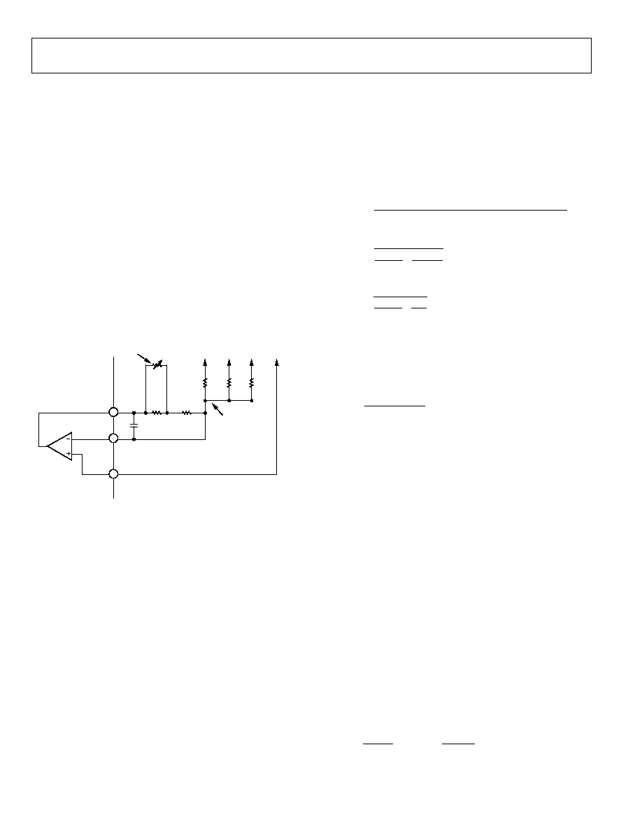
INDUCTOR DCR TEMPERATURE CORRECTION
With the inductor's DCR being used as sense element, and
copper wire being the source of the DCR, one needs to
compensate for temperature changes of the inductor's winding.
Fortunately, copper has a well-known temperature coefficient
(TC) of 0.39%/∞C.
If R
CS
is designed to have an opposite sign but equal percentage
change in resistance, it cancels the temperature variation of the
inductor's DCR. Due to the nonlinear nature of NTC
thermistors, series resistors, R
CS1
and R
CS2
(see Figure 11) are
needed to linearize the NTC and produce the desired
temperature coefficient tracking.
18
CSCOMP
ADP3206
CSSUM
C
CS
R
CS1
R
CS2
R
PH1
R
TH
R
PH2
TO SWITCH
NODES
PLACE AS CLOSE AS POSSIBLE
TO NEAREST INDUCTOR
OR LOW-SIDE MOSFET
TO
V
OUT
SENSE
R
PH3
CSREF
04651-0-011
17
16
KEEP THIS PATH
AS SHORT AS
POSSIBLE AND
WELL AWAY FROM
SWITCH NODE LINES
Figure 11. Temperature Compensation Circuit Values
The following procedure and expressions yield values for
R
CS1
, R
CS2
, and R
TH
(the thermistor value at 25∞C) for a given
R
CS
value.
1.
Select an NTC to be used based on type and value. Because
we do not have a value yet, start with a thermistor with a
value close to R
CS
. The NTC should also have an initial
tolerance of better than 5%.
2.
Based on the type of NTC, find its relative resistance value
at two temperatures. The temperatures to use that work
well are 50∞C and 90∞C. We call these resistance values A
(A is R
TH
(50∞C)/R
TH
(25∞C)) and B (B is
R
TH
(90∞C)/R
TH
(25∞C)). Note that the NTC's relative value
is always 1 at 25∞C.
3.
Next, find the relative value of R
CS
required for each
of these temperatures. This is based on the percentage
change needed, which we initially make 0.39%/∞C.
We call these r
1
(r
1
is 1/(1+ TC ◊ (T
1
- 25))) and
r
2
(r
2
is 1/(1 + TC ◊ (T
2
- 25))), where TC=0.0039,
T1 = 50∞C and T2 = 90∞C.
4.
Compute the relative values for R
CS1
, R
CS2
, and R
TH
using:
)
(
)
1
(
)
1
(
)
1
(
)
1
(
)
(
B
A
r
A
B
r
B
A
r
A
B
r
B
A
r
r
B
A
r
2
1
1
2
2
1
CS2
-
-
◊
-
◊
-
◊
-
◊
◊
-
◊
+
◊
-
◊
-
◊
◊
-
=
CS2
1
CS2
CS1
r
r
A
r
A
r
-
-
-
-
=
1
1
)
1
(
CS1
CS2
TH
r
r
r
1
1
1
1
-
-
=
(8)
5.
Calculate R
TH
= r
TH
◊
R
CS
, then select the closest value of
thermistor available. Also compute a scaling factor k based
on the ratio of the actual thermistor value used relative to
the computed one:
(
)
(
)
CALCULATED
TH
ACTUAL
TH
R
R
k =
(9)
6.
Finally, calculate values for R
CS1
and R
CS2
using:
CS1
CS
CS1
r
k
R
R
◊
◊
=
))
(
)
1
((
CS2
CS
CS2
r
k
k
R
R
◊
+
-
◊
=
(10)
For this example, we start with a thermistor value of 100 k.
Looking through available 0603 size thermistors, we can find
a Vishay NTHS0603N01N1003JR NTC thermistor with
A = 0.3602 and B = 0.09174. From these data we compute
r
CS1
= 0.3796, r
CS2
= 0.7195 and r
TH
= 1.0751. Solving for R
TH
yields 107.5 k, so we choose 100 k, making k = 0.9302.
Finally, we find R
CS1
and R
CS2
to be 35.3 k and 73.9 k.
Choosing the closest 1% resistor values yields a choice of
35.7 k and 73.2 k.
OUTPUT OFFSET
Intel's specification requires that at no load the nominal output
voltage of the regulator to be offset to a lower value than the
nominal voltage corresponding to the VID code. The offset is
set by a constant current source flowing out of the FB pin (I
FB
)
and flowing through R
B
. The value of R
B
can be found using the
following equation. The closest standard 1% resistor value is
1.58 k.
FB
OFFSET
B
I
V
R =
(11)
k
67
.
1
A
15
V
025
.
0
=
=
B
R

ADP3206
Rev. 0| Page 21 of 32
C
OUT
SELECTION
The required output decoupling for processors and platforms is
typically recommended by Intel. The following guidelines can
also be used if there are both bulk and ceramic capacitors in
the system.
The first thing is to select the total amount of ceramic
capacitance. This is based on the number and type of capacitor
to be used. The best location for ceramics is inside the socket;
12 to 18 pieces of size 1206 being the physical limit. Others can
be placed along the outer edge of the socket as well.
Combined ceramic values of 200 to 300 µF are recommended,
and are usually made up of multiple 10 µF or 22 µF capacitors.
Select the number of ceramics and find the total ceramic
capacitance (C
Z
).
Next, there is an upper limit imposed on the total amount of
bulk capacitance (C
X
) when one considers the VID on-the-fly
output voltage stepping (voltage step V
V
in time t
V
with error of
V
ERR
), and also a lower limit based on meeting the critical
capacitance for load release at a given maximum load step I
O
.
The IMVP-5 specification allows a maximum Vcore overshoot
(V
OSMAX
) of 50 mV over VID voltage for a step-off load current.
Z
O
OFFSET
OSMAX
O
VID
O
MIN
X
C
I
V
V
R
V
n
I
L
C
-
+
+
◊
◊
◊
)
(
(12)
(
)
MAX
X
C
Z
O
V
VID
V
VID
V
2
O
2
C
L
nkR
V
V
t
V
V
R
nK
L
-
-
◊
+
◊
◊
1
1
2
=
V
VERR
V
V
n
K
1
where
To meet the conditions of these expressions and transient
response, the ESR of the bulk capacitor bank (R
X
) should be less
than two times the droop resistance, R
O
. If the C
X(MIN)
is larger
than C
X(MAX)
, the system does not meet the VID on-the-fly
and/or Deepersleep exit specification and may require a smaller
inductor or more phases (the switching frequency may also
have to be increased to keep the output ripple the same).
For our example, we use thirty pieces of 10 µF 0805 MLC
capacitors (C
Z
= 300 µF). The largest VID voltage change is the
exit of Deepersleep, V
CORE
change is 525 mV in 100 µs with a
setting error of 20 mV. Where K = 3.3, solving for the bulk
capacitance yields:
mF
9
.
1
F
300
A
56
mV
25
mV
50
m
3
.
1
350
.
1
4
A
56
nH
560
)
(
=
µ
-
+
+
◊
◊
◊
MIN
X
C
Using six 330 µF Panasonic SP capacitors with a typical ESR of
7 m each yields C
X
= 1.98 mF with an R
X
= 1.2 m.
One last check should be made to ensure that the ESL of the
bulk capacitors (L
X
) is low enough to limit the initial high-
frequency transient spike. This is tested using:
pH
507
)
m
3
.
1
(
F
300
2
2
=
◊
◊
X
O
Z
X
L
R
C
L
(14)
In this example, L
X
is about 150 pH for the six SP cap capacitors,
which satisfies this limitation. If the L
X
of the chosen bulk
capacitor bank is too large, the number of capacitors must be
increased. One should note, for this multimode control
technique, an all-ceramic capacitor design can be used as long
as the conditions of Equations 12, 13 and 14 are satisfied.
POWER MOSFETS
For normal 20 A per phase application, the N-channel power
MOSFETs are selected for two high-side switches and two or
three low-side switches per phase. The main selection param-
eters for the power MOSFETs are V
GS(TH)
, Q
G
, C
ISS
, C
RSS
and
R
DS(ON)
. Because the gate drive voltage (the supply voltage to the
ADP3419) is 5 V, logic-level threshold MOSFETs must be used.
The maximum output current I
O
determines the R
DS(ON)
requirement for the low-side (synchronous) MOSFETs. In the
ADP3206, currents are balanced between phases; the current in
each low-side MOSFET is the output current divided by the
total number of MOSFETs (n
SF
). With conduction losses being
dominant, the following expression shows the total power being
dissipated in each synchronous MOSFET in terms of the ripple
current per phase (I
R
) and average total output current (I
O
):
(
)
( )
SF
DS
SF
R
SF
O
SF
R
n
I
n
n
I
D
P
◊
◊
+
◊
-
=
2
2
12
1
1
(15)
Knowing the maximum output current and the maximum
allowed power dissipation, one can find the required R
DS(ON)
for
the MOSFET. For SO-8 or SO-8 compatible packaged
MOSFETs, the junction to ambient (PCB) thermal impedance is
50∞C/W. In worst case, the PCB temperature is 70∞C to 80∞C
during heavy load operation of the notebook, a safe limit for P
SF
is 0.8 W~1.0 W at 120∞C junction temperature. Thus, for our
example (80 A maximum), we find R
DS(SF)
(per MOSFET) <
8.5m for two pieces of low-side MOSFET. This R
DS(SF
)
is also at
a junction temperature of about 120∞C, therefore, the R
DS(SF)
(per MOSFET) should be lower than 6 m at room
temperature, which gives 8.5 m at high temperature.
Another important factor for the synchronous MOSFET is the
input capacitance and feedback capacitance. The ratio of the
feedback to input needs to be small (less than 10% is
recommended) to prevent accidental turn-on of the
synchronous MOSFETs when the switch node goes high.

ADP3206
Rev. 0| Page 22 of 32
The high-side (main) MOSFET has to be able to handle two
main power dissipation components; conduction and switching
losses. The switching loss is related to the amount of time it
takes for the main MOSFET to turn on and off, and to the
current and voltage that are being switched. Basing the
switching speed on the rise and fall time of the gate driver
impedance and MOSFET input capacitance, the following
expression provides an approximate value for the switching loss
per main MOSFET, where n
MF
is the total number of main
MOSFETs:
(
)
ISS
MF
G
MF
O
CC
SW
MF
S
C
n
n
R
n
I
V
f
P
◊
◊
◊
◊
◊
◊
= 2
(16)
Here, R
G
is the total gate resistance (1.5 for the ADP3419
and about 0.5 for two pieces of typical high speed switching
MOSFETs, making R
G
= 2 ) and C
ISS
is the input capacitance
of the main MOSFET. The best thing to reduce switching loss is
to use lower gate capacitance devices.
The conduction loss of the main MOSFET is given by the
following, where
R
DS(MF)
is the ON-resistance of the MOSFET:
(
)
(
)
MF
DS
MF
R
MF
MF
C
R
n
I
n
n
D
P
◊
◊
◊
+
◊
=
2
2
O
12
1
I
(17)
Typically, for main MOSFETs, one wants the highest speed (low
C
ISS
) device, but these usually have higher ON-resistance. One
must select a device that meets the total power dissipation
(0.8~1.0 W for a single SO-8 package) when combining the
switching and conduction losses.
For our example, we have selected a Vishay SI7860 device as the
main MOSFET (eight in total; i.e., n
MF
= 8), with about C
ISS
=
1560 pF (max) and R
DS(MF)
= 15 m (max at Tj = 120∞C) and a
Vishay SI7889 device as the synchronous MOSFET (eight in
total; i.e., n
SF
= 8), R
DS(SF)
= 7.9 m (max at Tj = 120∞C). Solving
for the power dissipation per MOSFET at I
O
= 80 A and I
R
=
8.0 A yields 700 mW for each synchronous MOSFET and
730 mW for each main MOSFET. A 3rd synchronous MOSFET
is an option to further increase the conversion efficiency and
reduce thermal stress.
One last thing to look at is the power dissipation in the driver
for each phase. This is best described in terms of the Q
G
for the
MOSFETs and is given by the following, where Q
GMF
is the total
gate charge for each main MOSFET and Q
GSF
is the total gate
charge for each synchronous MOSFET:
(
)
SW
DRV
MF
GMF
SF
GSF
CC
CC
f
P
=
n
Q
+n
Q
+I
V
n
2
◊
◊
◊
◊
◊
(18)
Also shown is the standby dissipation (I
CC
times the V
CC
) of the
driver. For the ADP3419, the maximum dissipation should be
less than 300 mW, considering its thermal impedance 220∞C/W
and the maximum temperature increase is 50∞C. For our
example, with I
CC
= 2 mA, Q
GMF
= 22.8 nC and Q
GSF
= 84 nC, we
find 160 mW dissipation in each driver, which is below the 300
mW dissipation limit. See the ADP3419 data sheet for details.
RAMP RESISTOR SELECTION
The ramp resistor (R
R
) is used for setting the size of the internal
PWM ramp. The value of this resistor is chosen to provide the
best combination of thermal balance, stability, and transient
response. Use this expression to determine a starting value:
k
81
3
pF
5
m
2
.
4
5
3
nH
0
60
0.2
3
=
◊
◊
◊
◊
=
◊
◊
◊
◊
=
R
R
DS
D
R
R
R
C
R
A
L
A
R
(19)
where A
R
is the internal ramp amplifier gain, A
D
is the current
balancing amplifier gain, R
DS
is the total low-side MOSFET
ON-resistance, and C
R
is the internal ramp capacitor value.
Another consideration in the selection of R
R
is the size of the
internal ramp voltage (see Equation 20). For stability and noise
immunity, keep this ramp size larger than 0.5 V. Taking this into
consideration, the value of R
R
is selected as 280 k.
The internal ramp voltage magnitude can be calculated using:
(
)
(
)
V
m
51
.
0
kHz
267
pF
5
k
83
3
V
5
1.
125
0.
1
0.2
1
=
◊
◊
◊
-
◊
=
◊
◊
◊
-
◊
=
R
SW
R
R
VID
R
R
V
f
C
R
V
D
A
V
(20)
The size of the internal ramp can be made larger or smaller. If it
is made larger, stability and transient response improves, but
thermal balance degrades. Likewise, if the ramp is made smaller,
thermal balance improves at the sacrifice of transient response
and stability. The factor of three in the denominator of equation
19 sets a minimum ramp size that gives an optimal balance for
good stability, transient response, and thermal balance.
COMP PIN RAMP
There is a ramp signal on the COMP pin due to the droop
voltage and output voltage ramps. This ramp amplitude adds to
the internal ramp to produce the following overall ramp signal
at the PWM input.
(
)
◊
◊
◊
◊
-
◊
-
=
O
X
SW
R
RT
R
C
f
n
D
n
V
V
1
2
1
(21)
For this example, the overall ramp signal is found to be 1.1V.

ADP3206
Rev. 0| Page 23 of 32
CURRENT LIMIT SETPOINT
To select the current limit set point, we need to find the resistor
value for R
LIM
. The current limit threshold for the ADP3206 is
set with a 1 V source (V
LIM
) across R
LIM
with a gain of 6 mV/µA
per phase. R
LIM
can be found using the following:
O
LIM
LIM
LIM
LIM
R
I
n
V
A
R
◊
◊
◊
=
(22)
For values of R
LIM
greater than 500 k, the current limit may be
lower than expected, so some adjustment of R
LIM
may be
needed. Here, I
LIM
is the average current limit for the output of
the supply. For our example, choosing 120 A for I
LIM
, we find
R
LIM
to be 154 k, which is a standard 1% resistance.
The per phase current limit described earlier has its limit
determined by the following:
(
)
(
)
2
R
MAX
DS
D
BIAS
R
MAX
COMP
PHLIM
I
R
A
V
V
V
I
-
◊
-
-
(23)
For the ADP3206, the maximum COMP voltage (V
COMP(MAX)
) is
3.3 V, the COMP pin bias voltage (V
BIAS
) is 1.2 V, and the
current balancing amplifier gain (A
D
) is 5. Using V
R
of 1.1 V,
and R
DS(MAX)
of 4.2 m (low-side ON-resistance at 150∞C), we
find a per-phase limit of 66 A.
This limit can be adjusted by changing the ramp voltage V
R
. But
make sure not to set the per-phase limit lower than the average
per-phase current (I
LIM
/n).
The per phase initial duty cycle limit at maximum input voltage
is:
(
)
RT
BIAS
MAX
COMP
MIN
LIM
V
V
V
D
D
D
-
◊
=
=
(24)
For this example, the duty cycle limit at maximum input voltage
is found to be 0.23 when D is 0.07.
FEEDBACK LOOP COMPENSATION DESIGN
Optimized compensation of the ADP3206 allows the best
possible response of the regulator's output to a load change. The
basis for determining the optimum compensation is to make
the regulator and output decoupling appear as an output
impedance that is entirely resistive over the widest possible
frequency range, including dc, and equal to the droop resistance
(R
O
). With the resistive output impedance, the output voltage
droops in proportion with the load current at any load current
slew rate; this ensures the optimal positioning and allows the
minimization of the output decoupling.
With the multimode feedback structure of the ADP3206, one
needs to set the feedback compensation to make the converter's
output impedance work in parallel with the output decoupling.
There are several poles and zeros created by the output inductor
and decoupling capacitors (output filter) that need to be
compensated for.
A type-three compensator on the voltage feedback is adequate
for proper compensation of the output filter. The expressions
given below are intended to yield an optimal starting point for
the design; some adjustments may be necessary to account for
PCB and component parasitic effects.(See Tuning Guide)
The first step is to compute the time constants for all of the
poles and zeros in the system:
(
)
VID
O
X
RT
VID
RT
L
DS
D
O
E
V
R
C
n
V
D
n
L
V
V
R
R
A
R
n
R
◊
◊
◊
◊
◊
-
◊
◊
+
◊
+
◊
+
◊
=
1
2
(25)
(
)
X
O
O
X
O
X
A
R
R
R
R
L
R
R
C
T
'
'
-
◊
+
-
◊
=
(26)
(
)
X
O
X
B
C
R
R
R
T
◊
-
+
=
'
(27)
E
VID
SW
DS
D
RT
C
R
V
f
R
A
L
V
T
◊
◊
◊
-
◊
=
2
(28)
(
)
O
Z
O
X
O
Z
X
D
R
C
R
R
C
R
C
C
T
◊
+
-
◊
◊
◊
=
'
2
(29)
where, for the ADP3206, R' is the PCB resistance from the bulk
capacitors to the ceramics and where R
DS
is the total low-side
MOSFET ON-resistance per phase. For this example, A
D
is 5,
V
RT
equals 1.1V, R' is approximately 0.4 m (assuming an
8-layer motherboard) and L
X
is 150 pH for the six Panasonic SP
capacitors.
The compensation values can be solved using the following:
B
E
A
O
A
R
R
T
R
n
C
◊
◊
◊
=
(30)
A
C
A
C
T
R =
(31)
B
B
B
R
T
C =
(32)
A
D
FB
R
T
C
=
(33)
The standard values for these components are subject to the
tuning procedure, as introduced in the next section.

ADP3206
Rev. 0| Page 24 of 32
C
IN
SELECTION AND INPUT CURRENT DI/DT
REDUCTION
In continuous inductor-current mode, the source current of the
high-side MOSFET is approximately a square wave with a duty
ratio equal to n ◊ V
OUT
/V
IN
and an amplitude of one-nth of the
maximum output current. To prevent large voltage transients, a
low ESR input capacitor sized for the maximum rms current
must be used. The maximum rms capacitor current happens at
the lowest input voltage, and is given by
A
4
.
9
1
166
.
0
4
1
A
80
66
.
01
1
1
=
-
◊
◊
◊
=
-
◊
◊
◊
=
CRMS
MAX
O
MAX
CRMS
I
D
N
I
D
I
(34)
In a typical notebook system, the battery rail decouplings are
MLCC capacitors or a mixture of MLCC capacitors and bulk
capacitors. In this example, the input capacitor bank is formed
by 12 pieces of 10 µF, 25 V MLCC capacitors with a ripple
current rating of about 1A each.
90
E
FFICIE
NCY
(%)
LOAD CURRENT (A)
75
80
85
10
20
30
40
50
60
70
80
90
VDC = 8V
VDC = 19V
04651-0-012
VDC = 12V
Figure 12. Efficiency of Power Conversion vs. Output Current and Input
Voltage
DEEPERSLEEP VOLTAGE AND TRANSIENT SETTING
The Deepersleep voltage is set on the DPRSET pin via a resistor
divider from V
REF
voltage, which is 3.0 V. The voltage set on the
DPRSET pin is used as the reference voltage for the error
amplifier when DPRSLP is asserted. Considering there is a zero
load offset voltage, the voltage on the DPRSET pin should be
V
DPRSET
= V
OFFSET
+V
DPRSLP
(35)
With
V
DPRSLP
= 0.8 V and
V
OFFSET
= 25 mV,
V
DPRSET
= 0.825 V.
The suggested current for the DPRSET pin resistor divider is
I
DPRSET
=50 µA. Therefore, the divider resistors are:
k
5
.
43
=
-
=
DPRSLP
DPRSET
REF
DPRSET1
I
V
V
R
(36)
k
5
.
16
=
=
DPRSLP
DPRSET
DPRSET2
I
V
R
(37)
The closest 1% resistors are 43.2 k and 16.5 k.
During the transient of entering and exiting Deepersleep, the
slew-rate of V
CORE
reference voltage change is controlled by the
STSET pin capacitance, which can be calculated as below.
DPRSLP
OFFSET
VIDHFM
STSET
DPRSLP
STSET
V
V
V
I
T
C
-
-
◊
◊
=
8
.
0
(38)
T
DPRSLP
is the longest duration of Deepersleep exit, specified as
100 µs in IMVP-5. I
STSET
is the charge and discharge current of
the STSET pin, and has a value of ±15 µA. V
VIDHFM
is the highest
possible VID voltage the system returns when it exits from
Deepersleep. It is specified as 1.350 V in IMVP-5. Therefore,
C
STSET
is calculated as 2.4 nF, with the closest standard
capacitance 2.2 nF.
Figure 4 shows the transition from active mode to Deepersleep
mode. As soon as DPRSLP is asserted, the V
CORE
voltage is
gradually discharged to Deepersleep voltage (0.8 V). Once the
transition is completed, the PWM outputs of phase 2, 3, and 4
are disabled, switching the converter to single-phase operation.
04651-0-013
Figure 13. Transient to Deepersleep Mode
Channel 1≠DPRSLP, Channel 2≠VCORE (with 1 V Offset),
Channel 3≠Switch Node of Phase 2, Channel 4≠SW node of Phase 1.
Figure 5 shows the power conversion efficiency improvement of
single-phase operation during Deepersleep.

ADP3206
Rev. 0| Page 25 of 32
E
FFICIE
NCY
(%)
LOAD CURRENT (A)
04651-0-014
90
30
50
70
3
4
5
6
2
1
0
1-PHASE OPERATION
4-PHASE OPERATION
Figure 14. Efficiency Improvement in Deepersleep Mode
DEEPSLEEP OFFSET VOLTAGE SETTING
The Deepsleep offset voltage is programmed by a resistor on the
DPSET pin. The voltage on the DPSET pin is equal to the VID
voltage. When DPSLP is asserted, the current programmed on
the DPSET pin is sourced on the FB pin, resulting in an
additional negative offset voltage. The DPSET pin resistor
should be:
FB
OS
OFFSET
DPSET
I
V
V
R
%
=
(39)
where V
OS%
is the Deepsleep offset percentage, specified as 1.7%
in IMVP-5. The V
OFFSET
over
I
FB
term is actually the R
B
resistance (see Output Offset section). Thus,
R
DPSET
is calculated
as 98 k, with the closest standard resistance 97.6 k.
PWRGD MASK TIMER SETTING
The PWRGD (Power Good) mask is programmed by the
capacitance on the PGMASK pin. During the period of
PWRGD masking, there is a source current (I
PGMASK
= 5 µA) out
of the PGMASK pin, to charge a capacitor, C
PGMASK
. PWRGD
masking is terminated when the voltage on the PGMASK pin
reaches V
PGMASK
= 3.0 V.
Thus, the capacitance on the PGMASK pin can be calculated as:
PGMASK
PGMASK
PGMASK
PGMASK
V
I
T
C
◊
=
(40)
In IMVP-5, the PWRGD mask time is defined as
T
PGMASK
= 100 µs
resulting in C
PGMASK
= 167 pF. Because the specified T
PGMASK
is
the maximum length of masking time, please select the next
lower standard capacitance: 150 pF.
SELECTING THERMAL MONITOR COMPONENTS
For single-point hot spot thermal monitoring, simply set R
TTSET1
equal to the NTC thermistor's resistance at the alarm tempera-
ture. For example, if VRTT alarm temperature is 100∞C and we
use a Vishay thermistor (NTHS-0603N011003J), whose resis-
tance is 100 k at 25∞C, and 6.8 k at 100∞C, then we simply
can set R
TTSET1
= R
TH1
(100∞C) to 6.8 k.
ADP3206
REFERENCE VOLTAGE (3.0V)
REF
T
TSENSE
C
TT
R
TH1
R
TTSET1
R
R
04651-0-015
Figure 15. Single-Point Thermal Monitoring
Multiple-point hot spots thermal monitoring can be
implemented as shown in Figure 16. If any of the monitored hot
spots reaches alarm temperature, VRTT signal is asserted. The
following calculation sets the alarm temperature:
e
Temperatur
Alarm
TH1
REF
FD
REF
FD
TTSET1
R
V
V
V
V
R
-
+
=
2
1
2
1
(41)
where V
FD
is the forward drop voltage of the parallel diode.
Because the forward current is very small, the forward drop
voltage is very low, i.e., 100 mV. Assuming the same 100∞C
alarm temperature used in the single-spot thermal monitoring
example, and the same Vishay thermistor, then the above
formula leads to R
TTSET
= 7.8 k, whose closest standard resistor
is 7.87 k (1%).
ADP3206
REFERENCE
VOLTAGE (3.0V)
REF
C
TT
R
R
VRTT
T
TSENSE
R
TTSET1
R
TTSET2
R
TTSETn
R
THn
R
TH2
R
TH1
V
FD
04651-0-016
Figure 16. Multiple-Point Thermal Monitoring
The number of hot spots monitored is not limited as long as the
current limit of REF pin (4 mA) is not exceeded. The alarm
temperature of each hot spot can be set differently by playing
different RTTSET1, RTTSET2, ...RTTSET
n
.

ADP3206
Rev. 0| Page 26 of 32
According to IMVP-5, the shortest duration of assertion and
de-assertion of VRTT single is 1 ms (T
VRTT
= 1 ms). This VRTT
duration is programmed by the RC timer (R
TTMASK
, C
TTMASK
) on
the TTMASK pin. If the RC timer is charged by the VCC
voltage (5.0 V), then the RC timer can be set according to the
following formula:
R
TTMASK
◊
C
TTMASK
=
2.8 ◊
T
VRTT
(42)
Select a standard capacitance
C
TTMASK
= 47 nF, and then the
above formula leads to
R
TTMASK
= 59.6 k, whose next larger
standard resistor is 62 k (5%).
TUNING PROCEDURE FOR ADP3206
1.
Build circuit based on compensation values computed
from design spreadsheet.
2.
Hook-up dc load to circuit, turn on and verify operation.
Check for jitter at no-load and full-load.
DC Loadline Setting
3.
Measure output voltage at no-load (V
NL
). Verify it is within
tolerance.
4.
Measure output voltage at full-load and at cold (V
FLCOLD
).
Let board set for ~10 minutes at full-load and measure
output (V
FLHOT
). If there is a change of more than a few
millivolts, adjust
R
CS1
and
R
CS2
using Equations 43 and 44.
(
)
(
)
)
(
)
(
FLHOT
NL
FLCOLD
NL
OLD
CS2
NEW
CS2
V
V
V
V
R
R
-
-
◊
=
(43)
5.
Repeat Step 4 until cold and hot voltage measurements
remain the same.
6.
Measure output voltage from no-load to full-load using 5 A
steps. Compute the load line slope for each change and
then average to get overall load line slope (R
OMEAS
).
7.
If R
OMEAS
is off from R
O
by more than 0.05 m, use the
following to adjust the R
PH
values;
(
)
(
)
O
OMEAS
OLD
PH
NEW
PH
R
R
R
R
◊
=
(45)
8.
Repeat steps 6-7 to check load line and repeat adjustments
if necessary.
9.
Once complete with dc load line adjustment, do not change
R
PH
, R
CS1
, R
CS2
, or R
TH
for rest of procedure.
10.
Measure output ripple at no-load and full-load with scope
and make sure it is within spec.
AC Loadline Setting
11.
Remove dc load from circuit and hook up dynamic load.
12.
Hook up scope to output voltage and set to dc coupling
with time scale at 100 µs/div.
13.
Set dynamic load for a transient step of about 40 A at
1 kHz with 50% duty cycle.
14.
Measure output waveform (may have to use dc offset on
scope to see waveform). Try to use vertical scale of
100 mV/div or finer.
15.
You see a waveform that looks something like Figure 17.
Use the horizontal cursors to measure V
ACDRP
and V
DCDRP
as shown. Do not measure the undershoot or overshoot
that happens immediately after the step.
V
ACDRP
V
DCDRP
04835-0-012
Figure 17. AC Loadline Waveform
16.
If the V
ACDRP
and V
DCDRP
are different by more than a
couple of millivolts, use the following to adjust C
CS
. You
may need to parallel different values to get the right one
because there are limited standard capacitor values
available (it is a good idea to have locations for two
capacitors in the layout for this).
(
)
(
)
DCDRP
ACDRP
OLD
CS
NEW
CS
V
V
C
C
◊
=
(46)
17.
Repeat steps 15-16 and repeat adjustments if necessary.
Once complete, do not change C
CS
for the rest of the
procedure.
18.
Set dynamic load step to maximum step size (do not use a
step size larger than you need) and verify output waveform
is square (which means V
ACDRP
and V
DCDRP
are equal).
Note: Makes sure load step slew rate and turn-on are set for a
slew rate of ~150-250 A/µs (for example, a load step of 50 A
should take 200-300 ns) with no overshoot.
Some dynamic
loads have an excessive turn-on overshoot if a minimum
current is not set properly (this is an issue if you are using a
VTT tool).

ADP3206
Rev. 0| Page 27 of 32
Initial Transient Setting
19.
With dynamic load still set at maximum step size, expand
scope time scale to see 2-5 µs/div. You see a waveform that
may have two overshoots and one minor undershoot (see
Figure 18). Here, V
DROOP
is the final desired value.
V
DROOP
V
TRAN1
V
TRAN2
04835-0-013
Figure 18. Transient Setting Waveform, Load Step
20.
If both overshoots are larger than desired, try making the
following adjustments in this order (NOTE--if these
adjustments do not change the response, you are limited by
the output decoupling). Check the output response each
time you make a change as well as the switching nodes (to
make sure it is still stable).
a.
Make ramp resistor larger by 25% (R
RAMP
).
b.
For V
TRAN1
, increase C
B
or increase switching
frequency.
c.
For V
TRAN2
, increase R
A
and decrease C
A
both by 25%.
21.
For load release (see Figure 19), if V
TRANREL
is larger than
the IMVP-5 specification, you do not have enough output
capacitance. You either need more capacitance or to make
the inductor values smaller (if you change inductors, you
need to start the design over using the spreadsheet and this
tuning guide).
V
DROOP
V
TRANREL
04835-0-014
Figure 19. Transient Setting Waveform, Load Release
Figure 20 shows the typical transient response using these
compensation values.
04651-0-020
(a)
04651-0-021
(b)
Figure 20. Typical Transient Response for Design Example
(a) Load Step, (b) Load Release

ADP3206
Rev. 0| Page 28 of 32
LAYOUT AND COMPONENT PLACEMENT
The following guidelines are recommended for optimal
performance of a switching regulator in a PC system.
GENERAL RECOMMENDATIONS
For good results, at least a four-layer PCB is recommended. This
should allow the needed versatility for control circuitry
interconnections with optimal placement, power planes for
ground, input, and output power, and wide interconnection
traces in the rest of the power delivery current paths. Keep in
mind that each square unit of 1 ounce copper trace has a
resistance of ~0.53 m at room temperature.
Whenever high currents must be routed between PCB layers,
vias should be used liberally to create several parallel current
paths so that the resistance and inductance introduced by these
current paths is minimized and the via current rating is not
exceeded.
If critical signal lines (including the output voltage sense lines of
the ADP3206) must cross through power circuitry, it is best if a
signal ground plane can be interposed between those signal
lines and the traces of the power circuitry. This serves as a
shield to minimize noise injection into the signals at the
expense of making signal ground a bit noisier.
An analog ground plane should be used around and under the
ADP3206 for referencing the components associated with the
controller. This plane should be tied to the nearest output de-
coupling capacitor ground and should not be tied to any other
power circuitry to prevent power currents from flowing in it.
The components around the ADP3206 should be located close
to the controller with short traces. The most important traces to
keep short and away from other traces are the FB and CSSUM
pins. See Figure 2 for details on layout for the CSSUM node.
The output capacitors should be connected as closely as possible
to the load (or connector) that receives the power (e.g., a
microprocessor core). If the load is distributed, the capacitors
should also be distributed, and generally in proportion to where
the load tends to be more dynamic.
Avoid crossing any signal lines over the switching power path
loop, described below.
POWER CIRCUITRY
The switching power path should be routed on the PCB to
encompass the shortest possible length in order to minimize
radiated switching noise energy (i.e., EMI) and conduction
losses in the board. Failure to take proper precautions often
results in EMI problems for the entire PC system as well as
noise-related operational problems in the power converter
control circuitry. The switching power path is the loop formed
by the current path through the input capacitors and the power
MOSFETs including all interconnecting PCB traces and planes.
The use of short and wide interconnection traces is especially
critical in this path for two reasons: it minimizes the inductance
in the switching loop, which can cause high-energy ringing, and
it accommodates the high current demand with minimal
voltage loss.
Whenever a power dissipating component (for example, a
power MOSFET) is soldered to a PCB, the liberal use of vias,
both directly on the mounting pad and immediately
surrounding it, is recommended. Two important reasons for this
are: improved current rating through the vias, and improved
thermal performance from vias extended to the opposite side of
the PCB where a plane can more readily transfer the heat to the
air. Make a mirror image of any pad being used to heat sink the
MOSFETs on the opposite side of the PCB to achieve the best
thermal dissipation to the air around the board. To further
improve thermal performance, the largest possible pad area
should be used.
The output power path should also be routed to encompass a
short distance. The output power path is formed by the current
path through the inductor, the output capacitors, and the load.
For best EMI containment, a solid power ground plane should
be used as one of the inner layers extending fully under all the
power components.
SIGNAL CIRCUITRY
The output voltage is sensed and regulated between the FB pin
and the FBRTN pin (which connects to the signal ground at the
load). In order to avoid differential mode noise pickup in the
sensed signal, the loop area should be small. Thus the FB and
FBRTN traces should be routed adjacent to each other atop the
power ground plane back to the controller.
The feedback traces from the switch nodes should be connected
as close as possible to the inductor. The CSREF signal should be
Kelvin connected to the center point of the copper bar which is
the V
CORE
common node for the inductors of all the phases.
The ADP3206 has a metal pad in the back side of the package.
This metal pad is not a ground node. Do not ground this metal
pad. In addition, vias under the ADP3206 are not
recommended, because the metal pad may short between vias.

ADP3206
Rev. 0| Page 29 of 32
OUTLINE DIMENSIONS
1
40
10
11
31
30
21
20
BOTTOM
VIEW
4.25
4.10 SQ
3.95
TOP
VIEW
6.00
BSC SQ
PIN 1
INDICATOR
5.75
BSC SQ
12∞ MAX
0.30
0.23
0.18
0.20 REF
SEATING
PLANE
1.00
0.85
0.80
0.05 MAX
0.02 NOM
COPLANARITY
0.08
0.80 MAX
0.65 TYP
4.50
REF
0.50
0.40
0.30
0.50
BSC
PIN 1
INDICATOR
0.60 MAX
0.60 MAX
0.25 MIN
COMPLIANT TO JEDEC STANDARDS MO-220-VJJD-2
Figure 21. 40-Lead Frame Chip Scale Package [LFCSP]
(CP-40)
Dimensions shown in millimeters

ADP3206
Rev. 0| Page 30 of 32
ORDERING GUIDE
Model
Temperature Package
Package Description
Package Option
ADP3206JCPZ-REEL
1
0∞C to +100∞C
Lead Frame Chip Scale Package
CP-40
1
Z = Pb-free part.

ADP3206
Rev. 0| Page 31 of 32
NOTES

ADP3206
Rev. 0| Page 32 of 32
NOTES
© 2004 Analog Devices, Inc. All rights reserved. Trademarks and
registered trademarks are the property of their respective owners.
D04651-0-4/04(0)