 | –≠–Ľ–Ķ–ļ—ā—Ä–ĺ–Ĺ–Ĺ—č–Ļ –ļ–ĺ–ľ–Ņ–ĺ–Ĺ–Ķ–Ĺ—ā: ADP3155 | –°–ļ–į—á–į—ā—Ć:  PDF PDF  ZIP ZIP |
REV. A
Information furnished by Analog Devices is believed to be accurate and
reliable. However, no responsibility is assumed by Analog Devices for its
use, nor for any infringements of patents or other rights of third parties
which may result from its use. No license is granted by implication or
otherwise under any patent or patent rights of Analog Devices.
a
ADP3155
One Technology Way, P.O. Box 9106, Norwood, MA 02062-9106, U.S.A.
Tel: 781/329-4700
World Wide Web Site: http://www.analog.com
Fax: 781/326-8703
© Analog Devices, Inc., 1999
5-Bit Programmable Triple Power Supply
Controller for Pentium
ģ
III Processors
FEATURES
Active Voltage Positioning with Gain and Offset
Adjustment
Optimal Compensation for Superior Load Transient
Response
VRM 8.2, VRM 8.3 and VRM 8.4-Compliant
5-Bit Digitally Programmable 1.3 V to 3.5 V Output
Dual N-Channel Synchronous Driver
Two Onboard Linear Regulator Controllers
Total Output Accuracy 1% Over Temperature
High Efficiency, Current-Mode Operation
Short Circuit Protection
Overvoltage Protection Crowbar Protects Micro-
processors, with No Additional External Components
Power Good Output
TSSOP-20 Package
APPLICATIONS
Desktop PC Power Supplies for:
Pentium II and Pentium III Processor Families
AMD-K6 Processors
VRM Modules
Pentium is a registered trademark of Intel Corporation.
All other trademarks are the property of their respective holders.
GENERAL DESCRIPTION
The ADP3155 is a highly efficient synchronous buck switching
regulator controller optimized for converting the 5 V main sup-
ply into the core supply voltage required by the Pentium III and
other high performance processors. The ADP3155 uses an
internal 5-bit DAC to read a voltage identification (VID) code
directly from the processor, which is used to set the output
voltage between 1.3 V and 3.5 V. The ADP3155 uses a current-
mode, constant off-time architecture to drive two external N-
channel MOSFETs at a programmable switching frequency that
can be optimized for size and efficiency. It also uses a unique
supplemental regulation technique called active voltage position-
ing to enhance load transient performance.
Active voltage positioning results in a dc/dc converter that meets
the stringent output voltage specifications for Pentium II and
Pentium III processors, with the minimum number of output
capacitors and the smallest footprint. Unlike voltage-mode and
standard current-mode architectures, active voltage positioning
adjusts the output voltage as a function of the load current so
that it is always optimally positioned for a system transient.
The ADP3155 provides accurate and reliable short circuit pro-
tection and adjustable current limiting. It also includes an inte-
grated overvoltage crowbar function to protect the microprocessor
from destruction in case the core supply exceeds the nominal
programmed voltage by more than 15%.
The ADP3155 contains two linear regulator controllers that are
designed to drive external N-channel MOSFETs. These linear
regulators are used to generate the auxiliary voltages (AGP,
GTL, etc.) required in most motherboard designs, and have
been designed to provide a high bandwidth load-transient re-
sponse. A pair of external feedback resistors sets each linear
regulator output voltage.
R4
20k
V
OLDO1
1 F
V
INLDO1
Q
LDO1
R3
V
CC
+12V
1 F
22 F
V
IN
+5V
+
C
IN
L
+
C
O
V
O
1.3V TO
3.5V
R
SENSE
1nF
C
COMP
CMP
R2
R1
150pF
V
CC
SD
DRIVE1
SENSE+
SENSE≠
DRIVE2
PGND
AGND
C
T
ADP3155
FB1
V
LDO1
VID0≠VID4
5-BIT CODE
Q1
Q2
R6
20k
V
OLDO2
1 F
V
INLDO2
Q
LDO2
FB2
V
LDO2
R5
CMP
Figure 1. Typical Application
FUNCTIONAL BLOCK DIAGRAM
CMPI
V
T1
V
REF
+5%
V
REF
≠5%
DELAY
V
REF
+15%
PWRGD
SENSE+
CROWBAR
OFF
IN
NONOVERLAP
DRIVE
Q
S
R
DRIVE1 DRIVE2 PGND
2R
SENSE≠
VLDO1
REFERENCE
FB1
VLDO2
FB2
V
REF
V
CC
SD
V
T2
CMPT
C
T
g
m
R
DAC
OFF-TIME
CONTROL
V
IN
SENSE≠
1.20V
CMP
VID0
VID2
VID3
VID4
ADP3155
AGND
VID1

REV. A
≠2≠
ADP3155≠SPECIFICATIONS
(0 C
T
A
+70 C, V
CC
= 12 V, V
IN
= 5 V, unless otherwise noted)
1
Parameter
Symbol
Conditions
Min
Typ
Max
Units
OUTPUT ACCURACY
1.3 V Output Voltage
V
O
(Figure 13)
1.283 1.3
1.317
V
2.0 V Output Voltage
1.980 2.0
2.020
V
3.5 V Output Voltage
3.465 3.5
3.535
V
OUTPUT VOLTAGE LINE
V
O
I
LOAD
= 10 A (Figure 2)
REGULATION
V
IN
= 4.75 V to 5.25 V
0.05
%
INPUT DC SUPPLY CURRENT
2
Normal Mode
I
Q
V
SD
= 0.6 V
4.1
5.5
mA
Shutdown
T
A
= +25
į
C, VID Pins Floating
140
250
Ķ
A
CURRENT SENSE THRESHOLD
VOLTAGE
V
SENSE(TH)
V
SENSE≠
Forced to V
OUT
≠ 3%
125
145
165
mV
VID0≠VID4 THRESHOLD
VID
(TH)
Low
0.6
V
High
2.0
V
VID0≠VID4 INPUT CURRENT
I
VID
VID = 0 V
110
220
Ķ
A
VID0≠VID4 PULL-UP RESISTANCE
R
VID
20
30
k
C
T
PIN DISCHARGE CURRENT
I
11
T
A
= +25
į
C
V
OUT
in Regulation
65
Ķ
A
V
OUT
= 0 V
2
10
Ķ
A
OFF-TIME
t
OFF
C
T
= 150 pF
1.8
2.45
3.2
Ķ
s
DRIVER OUTPUT TRANSITION
t
R
, t
F
C
L
= 7000 pF (Pins 17, 18)
TIME
T
A
= +25
į
C
120
200
ns
POSITIVE POWER GOOD TRIP POINT
3
V
PWRGD
% Above Output Voltage
5
8
%
NEGATIVE POWER GOOD TRIP POINT
3
V
PWRGD
% Below Output Voltage
≠8
≠5
%
POWER GOOD RESPONSE TIME
t
PWRGD
500
Ķ
s
CROWBAR TRIP POINT
V
CROWBAR
% Above Output Voltage
9
15
24
%
ERROR AMPLIFIER
OUTPUT IMPEDANCE
RO
ERR
275
k
ERROR AMPLIFIER
TRANSCONDUCTANCE
g
m(ERR)
2.2
mmho
ERROR AMPLIFIER MINIMUM
OUTPUT VOLTAGE
V
CMPMIN
V
SENSE+
Forced to V
OUT
+ 3%
0.8
V
ERROR AMPLIFIER MAXIMUM
OUTPUT VOLTAGE
V
CMPMAX
V
SENSE+
Forced to V
OUT
≠ 3%
2.4
V
ERROR AMPLIFIER BANDWIDTH ≠3 dB
BW
ERR
CMP = Open
500
kHz
LINEAR REGULATOR FEEDBACK
CURRENT
I
FB
0.35
1
Ķ
A
LINEAR REGULATOR
V
OLDO1
,
Figure 2, R3 = R5 = 20 k
OUTPUT VOLTAGE
V
OLDO2
R4 = R6 = 35 k
, I
O
= 1 A
3.24
3.30
3.38
V
SHUTDOWN (SD) PIN
Low Threshold
SD
L
Part Active
0.6
V
High Threshold
SD
H
Part in Shutdown
2.0
V
Input Current
SD
IC
10
Ķ
A
NOTES
1
All limits at temperature extremes are guaranteed via correlation using standard Statistical Quality Control (SQC) methods.
2
Dynamic supply current is higher due to the gate charge being delivered to the external MOSFETs.
3
The trip point is for the output voltage coming into regulation.
Specifications subject to change without notice.
REV. A
ADP3155
≠3≠
PIN FUNCTION DESCRIPTIONS
Pin No.
Mnemonic
Function
1≠4, 20
VID1≠VID4,
Voltage Identification DAC Inputs. These pins are pulled up to an internal reference, providing a
VID0
Logic 1 if left open. The DAC output programs the SENSE≠ regulation voltage from 1.3 V to 3.5 V.
Leaving all five DAC inputs open results in placing the ADP3155 into shutdown.
5
AGND
Analog Ground. All internal signals of the ADP3155 are referenced to this ground.
6
SD
Shutdown. A logic high will place the ADP3155 in shutdown and disable both outputs. This pin is
internally pulled down.
7, 14
FB1, FB2
These pin are the feedback connections for the linear controllers. Connect each pin to the resistor
divider from each respective linear regulator output to set its output voltage.
8, 13
V
LDO1
, V
LDO2
Gate drives for the respective linear regulator N-channel MOSFETs.
9
SENSE≠
Connects to the internal resistor divider that senses the output voltage. This pin is also the reference
input for the current comparator.
10
SENSE+
The (+) input for the current comparator. The output current is sensed as a voltage at this pin with
respect to SENSE≠.
11
C
T
External capacitor C
T
connection to ground sets the off time of the device.
12
CMP
Error Amplifier output and compensation point. The voltage at this output programs the output cur-
rent control level between the SENSE pins.
15
PWRGD
Power Good. An open drain signal indicates that the output voltage is within a
Ī
5% regulation band.
16
V
CC
Supply Voltage to ADP3155.
17
DRIVE2
Gate Drive for the (bottom) synchronous rectifier N-channel MOSFET. The voltage at DRIVE2
swings from ground to V
CC
.
18
DRIVE1
Gate Drive for the buck switch N-channel MOSFET. The voltage at DRIVE1 swings from ground to
V
CC
.
19
PGND
Power Ground. The drivers turn off the buck and synchronous MOSFETs by discharging their gate
capacitances to this pin. PGND should have a low impedance path to the source of the synchronous
MOSFET.
PIN CONFIGURATION
TOP VIEW
(Not to Scale)
20
19
18
17
16
15
14
13
12
11
1
2
3
4
5
6
7
8
9
10
ADP3155
SENSE+
SENSE≠
V
LDO1
VID2
VID3
VID4
FB1
SD
AGND
C
T
CMP
V
LDO2
PGND
DRIVE1
DRIVE2
FB2
PWRGD
V
CC
VID1
VID0
ABSOLUTE MAXIMUM RATINGS*
Input Supply Voltage (V
CC
) . . . . . . . . . . . . . . ≠0.3 V to +16 V
Shutdown Input Voltage . . . . . . . . . . . . . . . . ≠0.3 V to +16 V
Operating Ambient Temperature Range . . . . . 0
į
C to +70
į
C
Junction Temperature Range . . . . . . . . . . . . . 0
į
C to +150
į
C
JA
. . . . . . . . . . . . . . . . . . . . . . . . . . . . . . . . . . . . 110
į
C/W
Storage Temperature Range . . . . . . . . . . . . ≠65
į
C to +150
į
C
Lead Temperature (Soldering, 10 sec) . . . . . . . . . . . +300
į
C
*This is a stress rating only; operation beyond these limits can cause the device to
be permanently damaged.
ORDERING GUIDE
Temperature
Package
Package
Model
Range
Description
Option
ADP3155JRU
0
į
C to +70
į
C
Thin Shrink Small RU-20
Outline (TSSOP)
CAUTION
ESD (electrostatic discharge) sensitive device. Electrostatic charges as high as 4000 V readily
accumulate on the human body and test equipment and can discharge without detection.
Although the ADP3155 features proprietary ESD protection circuitry, permanent damage may
occur on devices subjected to high energy electrostatic discharges. Therefore, proper ESD
precautions are recommended to avoid performance degradation or loss of functionality.
WARNING!
ESD SENSITIVE DEVICE
REV. A
ADP3155
≠4≠
P
SYSTEM
R1
150k
R2
39k
C
T
200pF
22 F
1 F
10BQ015
1 F
ESR = 25m
EACH
2200 F 3
L2
1 H
L1
1.7 H
R
SENSE
5m
ESR = 25m
EACH
2200 F
6
V
O
2V
0≠19A
RTN
220
100k
V
IN
+5V
+5V RTN
+12V RTN
C
COMP
2nF
1000 F
IRF3103
1nF
R4
5k
RTN
220
V
IN
+12V
2k
470pF
R3
20k
V
LDO1
+1.5V
4A
V
IN
+1.8V
Q4
IRLR3703
1000 F
R6
21.7k
R5
20k
1 F
V
INLDO2
+3.3V
V
LDO2
+2.5V
0≠2A
RTN
Q1
IRL3803
Q2
IRL3803
2k
470pF
1 F
22
ADP3155
SENSE+
SENSE≠
V
LDO1
VID2
VID3
VID4
FB1
SD
AGND
VID1
C
T
CMP
V
LDO2
PGND
DRIVE1
DRIVE2
FB2
PWRGD
V
CC
VID0
1
2
3
4
5
6
7
8
9
10
20
19
18
17
16
15
14
13
12
11
Figure 2. Typical VRM8.2/8.3/8.4 Compliant Core DC/DC Converter Circuit
g
m
NONOVERLAP
DRIVE
IN
CROWBAR
15
16
SD
V
CC
DRIVE1 DRIVE2 PGND
V
REF
+ 15%
5
AGND
PWRGD
SENSE+
DELAY
V
REF
+ 5% V
REF
≠ 5%
SENSE≠
2R
ADP3155
CMPI
DAC
CMP
1.20V
VID0
1
VID1
2
VID2
3
VID3
4
VID4
V
REF
V
T1
CMPT
V
T2
C
T
SENSE≠
6
REFERENCE
R
9
10
S
R
Q
OFF-TIME
CONTROL
V
IN
12
11
8
V
LDO1
FB1
OFF
18
17
13
V
LDO2
FB2
14
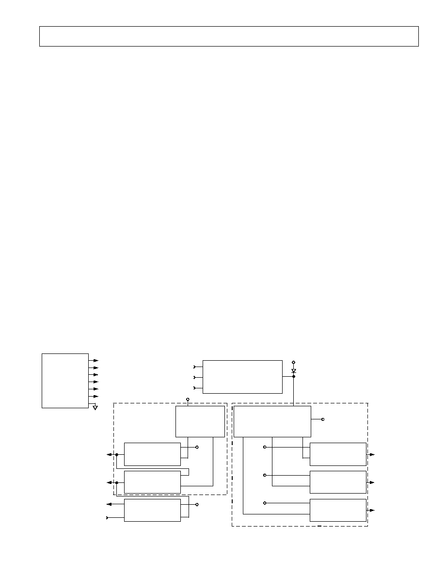
Figure 3. Functional Block Diagram
REV. A
ADP3155
≠5≠
OUTPUT CURRENT ≠ Amps
EFFICIENCY ≠ %
100
65
1.4
2.8
14
4.2
5.6
7
9.8 11.2 12.6
8.4
95
85
80
75
70
90
V
OUT
= 2.0V
V
OUT
= 2.8V
V
OUT
= 3.5V
SEE FIGURE 2
V
OUT
= 1.3V
Figure 4. Efficiency vs. Output
Current
I
OUT
= 10A
2
500ns/DIV
1
PRIMARY
N-DRIVE
DRIVER OUTPUT
SECONDARY
N-DRIVE
DRIVER OUTPUT
DRIVE 1 AND 2 = 5V/DIV
SEE FIGURE 2
Figure 7. Gate Switching Waveforms
OUTPUT CURRENT
1A TO 19A
OUTPUT VOLTAGE
20mV/DIV
10 s/DIV
Figure 10. Transient Response,
1 A≠19 A of Figure 2 Circuit
TIMING CAPACITOR ≠ pF
50
100
800
200
300
400
500
600
700
FREQUENCY ≠ kHz
450
400
0
200
150
100
50
350
250
300
Figure 5. Frequency vs. Timing
Capacitor
100ns/DIV
SEE FIGURE 2
V
CC
= +12V
V
IN
= +5V
I
OUT
= 10A
Figure 8. Driver Transition
Waveforms
3
4
10ms/DIV
REGULATOR
OUTPUT VOLTAGE
1V/DIV
V
CC
VOLTAGE
5V/DIV
Figure 11. Power-On Start-Up
Waveform
OPERATING FREQUENCY ≠ kHz
45
397
58
83
134
SUPPLY CURRENT ≠ mA
45
40
0
20
15
10
5
35
25
30
Q
GATE(TOTAL)
= 100nC
Figure 6. Supply Current vs.
Operating Frequency
10 s/DIV
OUTPUT CURRENT
19A TO 1A
OUTPUT VOLTAGE
20mV/DIV
Figure 9. Transient Response,
19 A≠1 A of Figure 2 Circuit
OUTPUT ACCURACY ≠ %
NUMBER OF PARTS
15
0
≠0.55
≠0.5
≠0.45
25
20
10
5
≠0.4
≠0.35
≠0.3
≠0.25
≠0.2
≠0.15
≠0.1
≠0.05
0
0.05
0.1
0.15
0.2
0.25
0.3
0.35
0.4
0.45
0.5
T
A
= +25 C
SEE FIGURE 13
Figure 12. Output Accuracy
Distribution, V
OUT
= 2.0 V
Typical Performance Characteristics≠
REV. A
ADP3155
≠6≠
V
CC
SD
DRIVE1
SENSE+
SENSE≠
DRIVE2
PGND
AGND
C
T
CMP
12V
1k
1 F
4700pF
0.1 F
V
OUT
1.2V
100k
0.1 F
ADP3155
OP27
VID0≠
VID4
5-BIT CODE
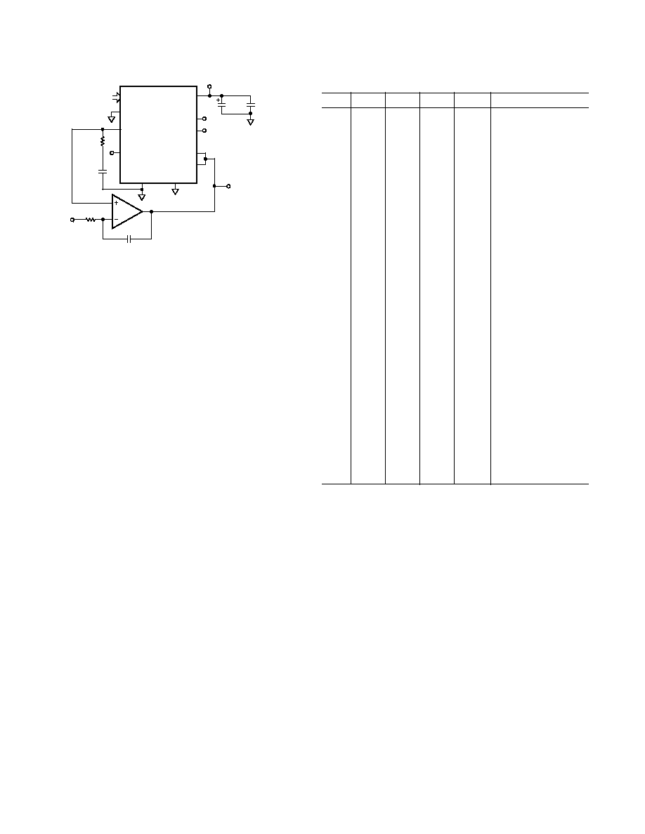
Figure 13. Closed-Loop Test Circuit for Accuracy
THEORY OF OPERATION
The ADP3155 uses a current-mode, constant-off-time control
technique to switch a pair of external N-channel MOSFETs in
a synchronous buck topology. Constant off-time operation
offers several performance advantages, including that no slope
compensation is required for stable operation. A unique feature
of the constant-off-time control technique is that since the off-
time is fixed, the converter's switching frequency is a function
of the ratio of input voltage to output voltage. The fixed off-
time is programmed by the value of an external capacitor con-
nected to the C
T
pin. The on-time varies in such a way that a
regulated output voltage is maintained as described below in the
cycle-by-cycle operation. Under fixed operating conditions the
on-time does not vary, and it varies only slightly as a function of
load. This means that switching frequency is fairly constant in
standard VRM applications. In order to maintain a ripple cur-
rent in the inductor that is independent of the output voltage
(which also helps control losses and simplify the inductor de-
sign), the off-time is made proportional to the value of the out-
put voltage. Normally, the output voltage is constant and,
therefore, the off-time is constant as well.
Active Voltage Positioning
The output voltage is sensed at the SENSE≠ pin. A voltage-
error amplifier, (g
m
), amplifies the difference between the output
voltage and a programmable reference voltage. The reference
voltage is programmed to between 1.3 V and 3.5 V by an inter-
nal 5-bit DAC, which reads the code at the voltage identifica-
tion (VID) pins. (Refer to Table I for output voltage vs. VID pin
code information.) A unique supplemental regulation technique
called active voltage positioning with optimal compensation
adjusts the output voltage as a function of the load current so
that it is always optimally positioned for a load transient. Stan-
dard (passive) voltage positioning, sometimes recommended for
use with other architectures, has poor dynamic performance
which renders it ineffective under the stringent repetitive tran-
sient conditions specified in Intel VRM documents. Conse-
quently, such techniques do not allow the minimum possible
number of output capacitors to be used. Optimally compen-
sated active voltage positioning as used in the ADP3155 pro-
vides a bandwidth for transient response that is limited only by
parasitic output inductance. This yields optimal load transient
response with the minimum number of output capacitors.
Table I. Output Voltage vs. VID Code
VID4
VID3
VID2
VID1
VID0
V
OUT
0
1
1
1
1
1.30
0
1
1
1
0
1.35
0
1
1
0
1
1.40
0
1
1
0
0
1.45
0
1
0
1
1
1.50
0
1
0
1
0
1.55
0
1
0
0
1
1.60
0
1
0
0
0
1.65
0
0
1
1
1
1.70
0
0
1
1
0
1.75
0
0
1
0
1
1.80
0
0
1
0
0
1.85
0
0
0
1
1
1.90
0
0
0
1
0
1.95
0
0
0
0
1
2.00
0
0
0
0
0
2.05
1
1
1
1
1
No CPU≠Shutdown
1
1
1
1
0
2.10
1
1
1
0
1
2.20
1
1
1
0
0
2.30
1
1
0
1
1
2.40
1
1
0
1
0
2.50
1
1
0
0
1
2.60
1
1
0
0
0
2.70
1
0
1
1
1
2.80
1
0
1
1
0
2.90
1
0
1
0
1
3.00
1
0
1
0
0
3.10
1
0
0
1
1
3.20
1
0
0
1
0
3.30
1
0
0
0
1
3.40
1
0
0
0
0
3.50
Cycle-by-Cycle Operation
During normal operation (when the output voltage is regulated),
the voltage-error amplifier and the current comparator (CMPI)
are the main control elements. (See the block diagram of Figure
3.) During the on-time of the high side MOSFET, CMPI moni-
tors the voltage between the SENSE+ and SENSE≠ pins. When
the voltage level between the two pins reaches the threshold level
V
T1
, the high side drive output is switched to ground, which
turns off the high side MOSFET. The timing capacitor C
T
is
then discharged at a rate determined by the off-time controller.
While the timing capacitor is discharging, the low side drive
output goes high, turning on the low side MOSFET. When the
voltage level on the timing capacitor has discharged to the thresh-
old voltage level V
T2
, comparator CMPT resets the SR flip-flop.
The output of the flip-flop forces the low side drive output to go
low and the high side drive output to go high. As a result, the low
side switch is turned off and the high side switch is turned on.
The sequence is then repeated. As the load current increases, the
output voltage starts to decrease. This causes an increase in the
output of the voltage-error amplifier, which, in turn, leads to an
increase in the current comparator threshold V
T1
, thus tracking
the load current. To prevent cross conduction of the external
MOSFETs, feedback is incorporated to sense the state of the driver
output pins. Before the low side drive output can go high, the
high side drive output must be low. Likewise, the high side drive
output is unable to go high while the low side drive output is high.
REV. A
ADP3155
≠7≠
Power Good
The ADP3155 has an internal monitor that senses the output
voltage and drives the PWRGD pin of the device. This pin is an
open drain output whose high level (when connected to a pull-
up resistor) indicates that the output voltage has been within a
Ī
5% regulation band of the targeted value for more than 500
Ķ
s.
The PWRGD pin will go low if the output is outside the regula-
tion band for more than 500
Ķ
s.
Output Crowbar
An added feature of using an N-channel MOSFET as the syn-
chronous switch is the ability to crowbar the output with the
same MOSFET. If the output voltage is 15% greater than the
targeted value, the ADP3155 will turn on the lower MOSFET,
which will current-limit the source power supply or blow its
fuse, pull down the output voltage, and thus save the micropro-
cessor from destruction. The crowbar function releases at ap-
proximately 50% of the nominal output voltage. For example, if
the output is programmed to 2.0 V, but is pulled up to 2.3 V or
above, the crowbar will turn on the lower MOSFET. If in this
case the output is pulled down to less than 1.0 V, the crowbar
will release, allowing the output voltage to recover to 2.0 V if
the fault condition has been removed.
Shutdown
The ADP3155 has a shutdown (SD) pin that is pulled down by
an internal resistor. In this condition the device functions nor-
mally. This pin should be pulled high to disable the output drives.
APPLICATION INFORMATION
A number of power conversion requirements must be consid-
ered when designing an ACPI compliant system. In normal
operating mode, 12 V, 5 V and 3.3 V are available from the
main supply. These voltages need to be converted into the
appropriate supply voltages for the Northbridge core, the
Southbridge core and RAMBUS memory, as well as supplies for
GTL and I/O drivers, CMOS memory and clock and graphics
(AGP) circuits.
During the standby operating state, the 12 V, 5 V and 3.3 V
power supply outputs are disabled, and only a low power 5 V
rail (5VSB) is available. The circuits that must remain active in
standby must be able to run from 5VSB. To accomplish this,
power routing is required to allow switching between normal
and standby supplies. Lack of a 12 V rail in standby makes control
of linear outputs difficult, and with up to 8 A demand from the
1.5 V and 1.8 V rails, an all-linear solution is inefficient.
Figure 14 shows a typical ACPI-compliant Pentium III/chipset
power management system using the ADP3155 and ADP3156.
The ADP3155 provides VID switched output and two linear
regulators for standby operation. A charge-pump-doubled 5VSB is
ORed into the supply rail to supply the linear regulators during
standby operation. The VID output collapses when the main
5 V rail collapses, but the N-channel MOSFET linear regu-
lators can continue to supply current from the ~9 V supply.
The ADP3156 provides 1.8 V via its main switching regulator,
and allows efficient linear regulation of 1.5 V rail by using the
1.8 V output as its source.
Specifications for a Design Example
The design parameters for a typical 300 MHz Pentium II appli-
cation (Figure 2) are as follows:
Input Voltage: V
IN
= 5 V
Auxiliary Input: V
CC
= 12 V
Output Voltage: V
O
= 2.8 V
Maximum Output Current:
I
OMAX
= 14.2 A dc
Minimum Output Current:
I
OMIN
= 0.8 A dc
Static tolerance of the supply voltage for the processor core:
V
OST+
= 100 mV
V
OST≠
= ≠60 mV
5V_PM
POWER
MANAGEMENT
FUNCTIONS
V
CC
12V
POWER MANAGEMENT
STATE COMMAND
5V_PM
ATX_POWER GOOD
PMSC
5V_PM
ATXPG
V
CC
ADP3155
VID_4:0
LIN#2_
CTRLS
LIN#1_
CTRLS
MAIN_
CTRLS
SWITCHER
IN
CTRLS
OUT
LINEAR#1
IN
CTRLS
OUT
LINEAR#2
IN
CTRLS
OUT
5V
5V_PM
CPU
V
CORE
@ VID
3.3V_PM
FOR POWER
MANAGEMENT
2.5V_PM
FOR CMOS,
CLOCK, MEMORY
TRIPLE
OUTPUT
SUPPLY
VID
V
CC
ADP3156
LIN_
CTRLS
MAIN_
CTRLS
12V
DUAL
OUTPUT
SUPPLY
IN
CTRLS
OUT
SWITCHER
5V
IN
CTRLS
OUT
LINEAR
3.3V_IN
1.5V_IN
VDDQ
POWER ROUTING
SELECT
3.3V
1.8V FOR
SB CORE,
MEM, ETC
1.5V VTT
FOR GTL
1.5V OR 3.3V
VDDQ FOR AGP
TYPEDET# FOR
AGP SELECT
ATX
(OR NLX)
POWER
SUPPLY
12V
5V
3.3V
5V_ALWAYS
ATX_PGOOD
ATX_SHUTDOWN
GND
12V
5V
3.3V
5V_PM
ATX_POWERGOOD
ATX_SHUTDOWN
Figure 14. ACPI-Compliant Pentium III System Block Diagram

REV. A
ADP3155
≠8≠
Transient tolerance (for less than 2
Ķ
s) of the supply voltage for
the processor core when the load changes between the mini-
mum and maximum values with a di/dt of 30 A/
Ķ
s:
V
OTR+
= 130 mV
V
OTR≠
= ≠130 mV
Input current di/dt when the load changes between the mini-
mum and maximum values: less than 0.1 A/
Ķ
s
The above requirements correspond to Intel's published power
supply requirements based on VRM 8.2 guidelines.
C
T
Selection for Operating Frequency
The ADP3155 uses a constant-off-time architecture with t
OFF
determined by an external timing capacitor C
T
. Each time the
high side N-channel MOSFET switch turns on, the voltage
across C
T
is reset to approximately 3.3 V. During the off time,
C
T
is discharged by a constant current of 65
Ķ
A. Once C
T
reaches 2.3 V, a new on-time cycle is initiated. The value of the
off-time is calculated using the continuous-mode operating
frequency. Assuming a nominal operating frequency of f
NOM
=
200 kHz at an output voltage of 2.8 V, the corresponding off
time is:
t
V
V
f
s
OFF
O
IN
NOM
=
=
1
1
2 2
≠
.
Ķ
The timing capacitor can be calculated from the equation:
C
t
A
V
pF
T
OFF
=
◊
=
65
1
143
Ķ
The converter operates at the nominal operating frequency only
at the above specified V
OUT
and at light load. At higher V
OUT
or
heavy load, the operating frequency decreases due to the para-
sitic voltage drops across the power devices. The actual mini-
mum frequency at V
OUT
= 2.8 V is calculated to be 160 kHz (see
Equation 1), where:
I
IN
is the input dc current
(assuming an efficiency of 90%, I
IN
= 9 A)
R
IN
is the resistance of the input filter
(estimated value: 7 m
)
R
DS(ON)HSF
is the resistance of the high side MOSFET
(estimated value: 10 m
)
R
DS(ON)LSF
is the resistance of the low side MOSFET
(estimated value: 10 m
)
R
SENSE
is the resistance of the sense resistor
(estimated value: 7 m
)
R
L
is the resistance of the inductor
(estimated value: 6 m
)
f
t
V
I
R
I
R
R
R
V
V
I
R
I
R
R
R
R
kHz
MIN
OFF
IN
IN
IN
OMAX
DS ON HSF
SENSE
L
O
IN
IN
IN
OMAX
DS ON HSF
SENSE
L
DS ON LSF
=
◊
+
+
+
+
=
1
160
≠
≠
(
)≠
≠
≠
(
≠
)
(
)
(
)
(
)
(1)
C
OUT
Selection--Determining the ESR
The required ESR and capacitance drive the selection of the
type and quantity of the output capacitors. The ESR must be
small enough that both the resistive voltage deviation due to a
step change in the load current and the output ripple voltage
stay below the values defined in the specification of the supplied
microprocessor. The capacitance must be large enough that the
output is held up while the inductor current ramps up or down
to the value corresponding to the new load current.
The total static tolerance of the Pentium II processor is 160 mV.
Taking into account the
Ī
1% setpoint accuracy of the ADP3155,
and assuming a 0.5% (or 14 mV) peak-to-peak ripple, the allowed
static voltage deviation of the output voltage when the load
changes between the minimum and maximum values is 80 mV.
Assuming a step change of
I = I
OMAX
≠I
OMIN
= 13.4 A, and
allocating all of the total allowed static deviation to the contri-
bution of the ESR sets the following limit:
R
ESR
mV
A
m
E MAX
MAX
(
)
.
.
=
=
=
1
80
13 4
5 9
The output filter capacitor must have an ESR of less than 5.9 m
.
One can use, for example, six FA-type capacitors from
Panasonic, with 2700
Ķ
F capacitance, 10 V voltage rating, and
34 m
ESR. The six capacitors have a total ESR of 5.7 m
when
connected in parallel, which gives adequate margin.
Inductor Selection
The minimum inductor value can be calculated from ESR, off-
time, dc output voltage and allowed peak-to-peak ripple voltage.
L
V t
R
V
V
s
m
mV
H
MIN
O OFF
E MAX
RIPPLE p
p
1
2 8
2 2
5 9
14
2 6
=
=
◊
◊
=
-
(
)
,
.
.
.
.
Ķ
Ķ
The minimum inductance gives a peak-to-peak ripple current of
2.15 A, or 15% of the maximum dc output current I
OMAX
.
The inductor peak current in normal operation is:
I
LPEAK
= I
OMAX
+ I
RPP
/2 = 15.3 A
The inductor valley current is:
I
LVALLEY
= I
LPEAK
≠ I
RPP
= 13 A
The inductor for this application should have an inductance
of 2.6
Ķ
H at full load current and should not saturate at the
worst-case overload or short circuit current at the maximum
specified ambient temperature. A suitable inductor is the
CTX12-13855 from Coiltronics, which is 4.4
Ķ
H at 1 A and
about 2.5
Ķ
H at 14.2 A.

REV. A
ADP3155
≠9≠
Tips for Selecting the Inductor Core
Ferrite designs have very low core loss, so the design should
focus on copper loss and on preventing saturation. Molypermalloy,
or MPP, is a low loss core material for toroids, and it yields the
smallest size inductor, but MPP cores are more expensive than
ferrite cores or the Kool M
Ķ
ģ
cores from Magnetics, Inc. The
lowest cost core is made of powdered iron, for example the #52
material from Micrometals, Inc., but yields the largest size
inductor.
C
OUT
Selection--Determining the Capacitance
The minimum capacitance of the output capacitor is determined
from the requirement that the output be held up while the in-
ductor current ramps up (or down) to the new value. The mini-
mum capacitance should produce an initial dv/dt that is equal
(but opposite in sign) to the dv/dt obtained by multiplying the
di/dt in the inductor and the ESR of the capacitor:
C
I
I
R
di dt
A
A
m
A
H
mF
MIN
OMAX
OMIN
E
=
=
-
◊
(
)
=
≠
(
/
)
.
.
.
.
/ .
.
14 2
0 8
5 9
2 2
4 4
4 5
Ķ
In the above equation the value of di/dt is calculated as the
smaller voltage across the inductor (i.e., V
IN
≠V
OUT
rather than
V
OUT
) divided by the maximum inductance (4.4
Ķ
H) of the
Coiltronics CTX12-13855 inductor. The six parallel-connected
2700
Ķ
F capacitors have a total capacitance of 16,200
Ķ
F, so the
minimum capacitance requirement is met with ample margin.
R
SENSE
The value of R
SENSE
is based on the required output current.
The current comparator of the ADP3155 has a threshold range
that extends from 0 mV to 125 mV (minimum). Note that the
full 125 mV range cannot be used for the maximum specified
nominal current, as headroom is needed for current ripple and
transients.
The current comparator threshold sets the peak of the inductor
current yielding a maximum output current, I
OMAX
, which equals
the peak value less half of the peak-to-peak ripple current. Solv-
ing for R
SENSE
allowing a 20% margin for overhead, and using
the minimum current sense threshold of 125 mV yields:
R
SENSE
= (125 mV)/[1.2(I
OMAX
+ I
RPP
/2)] = 6.8 m
Once R
SENSE
has been chosen, the peak short-circuit current
I
SC(PK)
can be predicted from the following equation:
I
SC(PK)
= (145 mV)/R
SENSE
= (145 mV)/(6.7 m
) = 21.5 A
The actual short-circuit current is less than the above calculated
I
SC(PK)
value because the off-time rapidly increases when the
output voltage drops below 1 V. The relationship between the
off-time and the output voltage is:
t
C
V
V
k
A
OFF
T
O
◊
+
1
360
2
Ķ
With a short circuit across the output, the off-time will be about
70
Ķ
s. During that time the inductor current gradually decays.
The amount of decay depends on the L/R time constant in the
output circuit. With an inductance of 2.5
Ķ
H and total resis-
tance of 23 m
, the time constant will be 108
Ķ
s. This yields a
valley current of 11.3 A and an average short-circuit current of
about 16.3 A. To safely carry the short-circuit current, the sense
resistor must have a power rating of at least 16.3 A
2
◊
6.8 m
=
1.8 W.
Current Transformer Option
An alternative to using a low value and high power current sense
resistor is to reduce the sensed current by using a low cost cur-
rent transformer and a diode. The current can then be sensed
with a small-size, low cost SMT resistor. Using a transformer
with one primary and 50 secondary turns reduces the worst-case
resistor dissipation to a few mW. Another advantage of using
this option is the separation of the current and voltage sensing,
which makes the voltage sensing more accurate.
Power MOSFETs
Two external N-channel power MOSFETs must be selected for
use with the ADP3155, one for the main switch and an identical
one for the synchronous switch. The main selection parameters
for the power MOSFETs are the threshold voltage V
GS(TH)
and
the on resistance R
DS(ON)
.
The minimum input voltage dictates whether standard threshold
or logic-level threshold MOSFETs must be used. For V
IN
> 8 V,
standard threshold MOSFETs (V
GS(TH)
< 4 V) may be used. If
V
IN
is expected to drop below 8 V, logic-level threshold MOSFETs
(V
GS(TH)
< 2.5 V) are strongly recommended. Only logic-level
MOSFETs with V
GS
ratings higher than the absolute maximum
of V
CC
should be used.
The maximum output current I
OMAX
determines the R
DS(ON)
requirement for the two power MOSFETs. When the ADP3155
is operating in continuous mode, the simplifying assumption can
be made that one of the two MOSFETs is always conducting
the average load current. For V
IN
= 5 V and V
OUT
= 2.8 V, the
maximum duty ratio of the high side FET is:
D
MAXHF
= (1 ≠ f
MIN
◊
t
OFF
) = (1 kHz≠160 kHz
◊
2.2
Ķ
s) = 65%
The maximum duty ratio of the low side (synchronous rectifier)
FET is:
D
MAXLF
= 1 ≠ D
MAXHF
= 35%
The maximum rms current of the high side FET is:
I
RMSHS
= [D
MAXHF
(I
LVALLEY
2 + I
LPEAK
2 + I
LVALLEY
I
LPEAK
)/3]
0.5
= 13.1 A rms
The maximum rms current of the low side FET is:
I
RMSLS
= [D
MAXLF
(I
LVALLEY
2 + I
LPEAK
2
+ I
LVALLEY
I
LPEAK
)/3]
0.5
= 8.41 A rms
The R
DS(ON)
for each FET can be derived from the allowable
dissipation. If 5% of the maximum output power is allowed for
FET dissipation, the total dissipation will be:
P
FETALL
= 0.05 V
O
I
OMAX
= 2 W
Allocating half of the total dissipation for the high side FET and
half for the low side FET, the required minimum FET resis-
tances will be:
R
DS(ON)HSF(MIN)
= 1.33 W/(11.5 A)
2
= 10 m
R
DS(ON)LSF(MIN)
= 0.67 W/(8.41 A)
2
= 9.5 m
Note that there is a trade-off between converter efficiency and
cost. Larger FETs reduce the conduction losses and allow
higher efficiency, but increase the system cost. If efficiency is
not a major concern, the International Rectifier IRL3103 is an
economical choice for both the high side and low side positions.
Those devices have an R
DS(ON)
of 14 m
at V
GS
= 10 V and at
+25
į
C. The low side FET is turned on with at least 10 V. The

REV. A
ADP3155
≠10≠
high side FET, however, is turned on with only 12 V ≠ 5 V = 7 V.
Checking the typical output characteristics of the device in the
data sheet shows that for an output current of 10 A, and at a
V
GS
of 7 V, the V
DS
is 0.15 V. This gives an R
DS(ON)
only slightly
above the one specified at a V
GS
of 10 V, so the resistance in-
crease due to the reduced gate drive can be neglected. The
specified R
DS(ON)
at the expected highest FET junction tempera-
ture of +140
į
C must be modified by an R
DS(ON)
multiplier,
using the graph in the data sheet. In this case:
R
DS(ON)MULT
= 1.7
Using this multiplier, the expected R
DS(ON)
at +140
į
C is 1.7
◊
14 m
= 24 m
.
The high side FET dissipation is:
P
DFETHS
= I
RMSHS
2
R
DS(ON)
+ 0.5 V
IN
I
LPEAK
Q
G
f
MIN
/I
G
~ 3.72 W
where the second term represents the turn-off loss of the FET.
(In the second term, Q
G
is the gate charge to be removed from
the gate for turn-off and I
G
is the gate current. From the data
sheet, Q
G
is about 50 nC≠70 nC and the gate drive current
provided by the ADP3155 is about 1 A.)
The low side FET dissipation is:
P
DFETLS
= I
RMSLS
2
R
DS(ON)
= 1.7 W
(Note that there are no switching losses in the low side FET.)
To maintain an acceptable MOSFET junction temperature,
proper heat sinks should be used. The Thermalloy 6030 heat
sink has a thermal impedance of 13
į
C/W with convection cool-
ing. With this heat sink, the junction-to-ambient thermal imped-
ance of the chosen high side FET
JAHS
will be 13
į
C/W (heat
sink-to-ambient) + 2
į
C/W (junction-to-case) + 0.5
į
C/W (case-
to-heat sink) = 15.5
į
C/W.
At full load, and at +50
į
C ambient temperature, the junction
temperature of the high side FET is:
T
JHSMAX
= T
A
+
JAHS
P
DFETHS
= +105
į
C
The same heat sink may be used for the low side FET, e.g., the
Thermalloy type 7141 (
= 20.3
į
C/W). With this heat sink, the
junction temperature of the low side FET is:
T
JLSMAX
= T
A
+
JALS
P
DFETLS
= +106
į
C
All of the above-calculated junction temperatures are safely
below the +175
į
C maximum specified junction temperature of
the selected FETs.
The maximum operating junction temperature of the ADP3155
is calculated as follows:
T
JICMAX
= T
A
+
JA
(I
IC
V
CC
+ P
DR
)
where
JA
is the junction-to-ambient thermal impedance of the
ADP3155 and P
DR
is the drive power. From the data sheet,
JA
is equal to 110
į
C/W and I
IC
= 2.7 mA. P
DR
can be calculated as
follows:
P
DR
= (C
RSS
+ C
ISS
)V
CC
2
f
MAX
= 307 mW
The result is:
T
JICMAX
= +86
į
C
C
IN
Selection and Input Current di/dt Reduction
In continuous inductor-current mode, the source current of the
high side MOSFET is a square wave with a duty ratio of V
OUT
/
V
lN
. To keep the input ripple voltage at a low value, one or more
capacitors with low equivalent series resistance (ESR) and ad-
equate ripple-current rating must be connected across the input
terminals. The maximum rms current of the input bypass
capacitors is:
I
CINRMS
= 0.5 I
OMAX
= 7 A rms
For an FA-type capacitor with 2700
Ķ
F capacitance and
10 V voltage rating, the ESR is 34 m
and the allowed ripple
current at 100 kHz is 1.94 A. At +105
į
C, at least four such
capacitors must be connected in parallel to handle the calculated
ripple current. At +50
į
C ambient, however, a higher ripple
current can be tolerated, so three capacitors in parallel are
adequate.
The ripple voltage across the three paralleled capacitors is:
V
CINRPL
= I
OMAX
[ESR
IN
/3 +D
MAXHF
/(3 C
IN
f
MIN
)] =
140 mV p-p
To further reduce the effect of the ripple voltage on the system
supply voltage bus and to reduce the input-current di/dt to
below the recommended maximum of 0.1 A/
Ķ
s, an additional
small inductor (L > 1.7
Ķ
H @ 10 A) should be inserted between
the converter and the supply bus (see Figure 2).
Feedback Loop Compensation Design for Active Voltage
Positioning
Optimized compensation of the ADP3155 allows the best pos-
sible containment of the peak-to-peak output voltage deviation.
Any practical switching power converter is inherently limited by
the inductor in its output current slew rate to a value much less
than the slew rate of the load. Therefore, any sudden change of
load current will initially flow through the output capacitors,
and this will produce an output voltage deviation equal to the
ESR of the output capacitor array times the load current change.
To correctly implement active voltage positioning, the low fre-
quency output impedance (i.e., the output resistance) of the
converter should be made equal to the maximum ESR of the
output capacitor array. This can be achieved by having a single
pole roll-off of the voltage gain of the g
m
error amplifier, where
the pole frequency coincides with the ESR zero of the output
capacitor. A gain with single pole roll-off requires that the g
m
amplifier output pin be terminated by the parallel combination
of a resistor and capacitor. The required resistor value can be
calculated from the equation:
R
k
Rt
k
Rt
C
TOTAL
TOTAL
=
◊
275
275
≠
where:
Rt
k
R
I
V
V
TOTAL
CS
OMAX
HI
LO
=
◊
◊
16 4
.
≠
and where the quantities 16.4 k
and 275 k
are characteristic
of the ADP3155 and the value of the current sense resistor, R
CS
,
has already been determined as above.
Although a single termination resistor equal to R
C
would yield
the proper voltage positioning gain, the dc biasing of that resis-
tor would determine how the regulation band is centered (i.e.,
offset). Note that sometimes the specified regulation band is
asymmetrical with respect to the nominal VID voltage. With the
ADP3155, the offset is already considered part of the design
procedure--no special provision is required. To accomplish the

REV. A
ADP3155
≠11≠
dc biasing, it is simplest to use two resistors to terminate the g
m
amplifier output, with the lower resistor tied to ground and the
upper resistor to the 12 V supply of the IC. The values of these
resistors can be calculated using:
R
R
V
V
UPPER
C
DIV
OS
=
◊
and:
R
R
V
V
V
LOWER
C
OS
DIV
OS
=
◊
≠
where V
DIV
is the resistor divider supply voltage (e.g., the rec-
ommended 12 V), and V
OS
is the offset voltage required on the
amplifier to produce the desired offset at the output. V
OS
is
calculated using Equation 2, where V
OUT(OS)
is the offset from
the nominal VID-programmed value to the center of the speci-
fied regulation window for the output voltage. (Note this may be
either positive or negative.) For clarification, that offset is given
by:
V
V
V
VID
OUT OS
HI
LO
(
)
(
)≠
=
+
1
2
where V
HI
and V
LO
are the respective upper and lower limits
allowed for regulation.
Finally, the compensating capacitance is determined from the
equality of the pole frequency of the error amplifier gain and the
zero frequency of the impedance of the output capacitor:
C
C
ESR
Rt
COMP
O
TOTAL
=
◊
Trade-Offs Between DC Load Regulation and AC Load
Regulation
Casual observation of the circuit operation--e.g., with a voltmeter
--would make it appear that the dc load regulation appears
to be rather poor compared to a conventional regulator. This
would be especially noticeable under very light or very heavy
loads where the voltage is "positioned" near one of the extremes
of the regulation window rather than near the nominal center
value. It must be noted and understood that this low gain char-
acteristic (i.e., loose dc load regulation) is inherently required to
allow improved transient containment (i.e., to achieve tighter ac
load regulation). That is, the dc load regulation is intentionally
sacrificed (but kept within specification) in order to minimize
the number of capacitors required to contain the load transients
produced by the CPU.
Linear Regulators
The two ADP3155 linear regulators provide a low cost, conve-
nient and versatile solution for generating additional lower sup-
ply rails that can be programmed in the range 1.2 V≠5 V. The
maximum output load current is determined by the size and
thermal impedance of the external N-channel power MOSFET
that is placed in series with the supply and controlled by the
ADP3155. The output voltage, V
OLDO1, 2
in Figure 14, is sensed
at the FB pin of the ADP3155 and compared to an internal
1.2 V reference in a negative feedback loop which keeps the
output voltage in regulation. If the load is being reduced or
increased, the FET drive will also be reduced or increased by the
ADP3155 to provide a well regulated
Ī
1% accurate output
voltage. The output voltage is programmed by adjusting the
value of the external resistor R
PROG
, shown in Figure 15.
Efficiency of the Linear Regulators
The efficiency and corresponding power dissipation of each of
the linear regulators are not determined by the ADP3155.
Rather, these are a function of input and output voltage and
load current. Efficiency is approximated by the formula:
= 100%
◊
(V
OUT
V
IN
)
The corresponding power dissipation in the MOSFET, together
with any resistance added in series from input to output is given
by:
P
LDO
= (V
IN(LDO)
≠ V
OUT(LDO)
)
◊
I
OUT(LDO)
Minimum power dissipation and maximum efficiency are ac-
complished by choosing the lowest available input voltage that
exceeds the desired output voltage. However, if the chosen
input source is itself generated by a linear regulator, its power
dissipation will be increased in proportion to the additional
current it must now provide. For most PC systems, the lowest
available input source for the linear regulators, which is not
itself generated by a linear regulator, is 3.3 V from the main
power supply.
Assuming that the 3.3 V supply is used to provide input power
for a 1.5 V linear regulator output, the efficiency will inherently
be 1.5 V 3.3 V, which is less than 50%. The total current
demand in all of the low voltage power rails (e.g., 1.5 V, 1.8 V
and 2.5 V) can produce unacceptable dissipation and junction
temperatures in the linear regulators. For such systems, Analog
Devices recommends the ADP3156--a switching regulator that
generates one of the lower voltage outputs (e.g., 1.8 V), which can
also be used as a power source to the lower voltage outputs
(e.g., 1.5 V). This results is a highly efficient and reliable power
conversion system that can readily handle the combined loading
specifications for the lower system voltages, with room to spare
for the higher current demands and lower voltages of next gen-
eration PC systems.
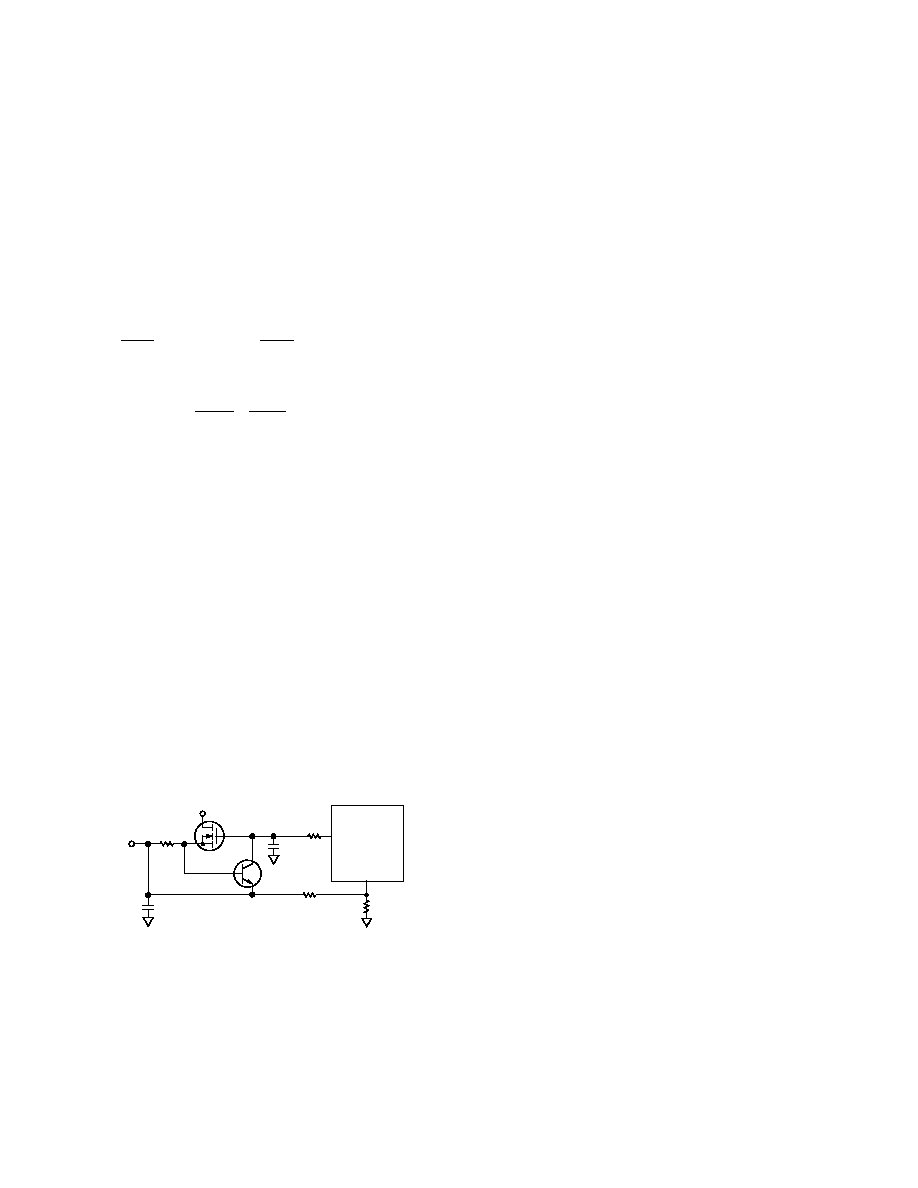
Features
∑ Tight DC Regulation Due to 1% Reference and High Gain
∑ Output Voltage Stays Within Specified Limits at Load
Current Step with 30 A/
Ķ
s Slope
∑ Fast Response to Input Voltage or Load Current Transients
Overcurrent protection may be provided by the addition of an
external NPN transistor and an external resistor R
S2
. The design
specification and procedure is given below.
V
R
Rt
V
V
Rt
k
V
Rt
k
R I
OS
C
TOTAL
OUT OS
TOTAL
TOTAL
CS OMAX
=
◊
+
+
0 8
1 36
1 7
275
6
.
.
≠ .
(
)
(2)
REV. A
ADP3155
≠12≠
Linear Regulator Design Example
Maximum Ambient Temperature . . . . . . . . . . . . T
A
= +50
į
C
Input Voltage . . . . . . . . . . . . . . . . . . . . . . . . . . . . . . V
IN
= 5 V
Output Voltage . . . . . . . . . . . . . . . . . . . . . . . . . . V
O2
= 3.3 V
Maximum Output Current . . . . . . . . . . . . . . . I
O2MAX
= 0.5 A
Maximum Output Load Transient Allowed . . . V
TR2
= 0.036 V
Chosen MOSFET . . . . . . . . . . . . . . . . . . . . . . . . . IRLR2703
Junction-to-Ambient Thermal Impedance (MOSFET)
1
JA
. . . . . . . . . . . . . . . . . . . . . . . . . . . . . . . . . . . . . 40
į
C/W
1
Uses 1-inch square PCB cu-foil as heat sink.
The output voltage may be programmed by the R
PROG
resistor
as follows:
R
V
V
k
V
V
k
k
PROG
O
=
◊
=
◊
=
2
1 2
1
20
3 3
1 2
1
20
35
.
≠
.
.
≠
The current sense resistor may be calculated as follows:
R
V
I
V
A
S
O MAX
2
2
0 54
0 54
0 5
1 1
=
=
=
.
.
.
.
The power rating is:
P
S2
= R
S2
◊
(I
O2MAX
◊
1.1)
2
= 0.33 W
Use a 0.5 W resistor.
The maximum FET junction temperature at shorted output is:
T
FETMAX
= T
A
+
(
JA
◊
V
IN
◊
I
O2MAX
◊
1.1) =
+50
į
C + (40
į
C/W
◊
5 V
◊
0.5 A
◊
1.1) = +160
į
C
which is within the maximum allowed by the FET's data sheet.
The maximum FET junction temperature at nominal output is:
T
FETMAX
= T
A
+ (
JA
◊
(V
IN
≠ V
O2
)
◊
I
O2MAX
)
=
+50
į
C + (40
į
C/W
◊
(5 V ≠ 3.3 V )
◊
0.5 A) = +84
į
C
The output filter capacitor maximum allowed ESR is:
ESR ~ V
TR2
/I
OMAX
= 0.036 V/0.5 A = 0.072
This requirement is met using a 1000
Ķ
F/10 V LXV series
capacitor from United Chemicon. For applications requiring
higher output current, a heat sink and/or a larger MOSFET
should be used to reduce the MOSFET's junction-to-ambient
thermal impedance.
R
S2
1.1
470pF
2N2222
V
IN
2k
1000 F/10V
V
OLDO1, 2
I
OLDO1, 2
V
LDO1, 2
ADP3155
FB1, 2
20k
R
PROG
35k
Figure 15. Linear Regulator with Overcurrent Protection
LAYOUT AND COMPONENT PLACEMENT GUIDELINES
The following guidelines are recommended for optimal perfor-
mance of a switching regulator in a PC system:
General Recommendations
1.
For best results, a four-layer (minimum) PCB is recom-
mended. This should allow the needed versatility for con-
trol circuitry interconnections with optimal placement, a
signal ground plane, power planes for both power ground
and the input power (e.g., 5 V), and wide interconnection
traces in the rest of the power delivery current paths. Each
square unit of 1 ounce copper trace has a resistance of
~0.53 m
at room temperature.
2.
Whenever high currents must be routed between PCB
layers, vias should be used liberally to create several parallel
current paths so that the resistance and inductance intro-
duced by these current paths is minimized and the via cur-
rent rating is not exceeded.
3.
The power and ground planes should overlap each other as
little as possible. It is generally easiest (although not neces-
sary) to have the power and signal ground planes on the
same PCB layer. The planes should be connected nearest
to the first input capacitor where the input ground current
flows from the converter back to the power source (e.g.,
5 V).
4.
If critical signal lines (including the voltage and current
sense lines of the ADP3155) must cross through power
circuitry, it is best if a signal ground plane can be inter-
posed between those signal lines and the traces of the
power circuitry. This serves as a shield to minimize noise
injection into the signals at the expense of making signal
ground a bit noisier.
5.
The PGND pin of the ADP3155 should connect first to a
ceramic bypass capacitor (on the V
CC
pin) and then into the
power ground plane using the shortest possible trace. How-
ever, the power ground plane should not extend under
other signal components, including the ADP3155 itself. If
necessary, follow the preceding guideline to use the signal
plane as a shield between the power ground plane and the
signal circuitry.
6.
The AGND pin of the ADP3155 should connect first to the
timing capacitor (on the C
T
pin), and then into the signal
ground plane. In cases where no signal ground plane can be
used, short interconnections to other signal ground cir-
cuitry in the power converter should be used--the compen-
sation capacitor being the next most critical.
7.
The output capacitors of the power converter should be
connected to the signal ground plane even though power
current flows in the ground of these capacitors. For this
reason, it is advised to avoid critical ground connections (e.g.,
the signal circuitry of the power converter) in the signal
ground plane between the input and output capacitors. It is
also advised to keep the planar interconnection path short
(i.e., have input and output capacitors close together).

REV. A
ADP3155
≠13≠
8.
The output capacitors should also be connected as closely
as possible to the load (or connector) that receives the
power (e.g., a microprocessor core). If the load is distrib-
uted, the capacitors also should be distributed, and gen-
erally in proportion to where the load tends to be more
dynamic.
9.
Absolutely avoid crossing any signal lines over the switching
power path loop, described below.
Power Circuitry
10. The switching power path should be routed on the PCB to
encompass the smallest possible area in order to minimize
radiated switching noise energy (i.e., EMI). Failure to take
proper precaution often results in EMI problems for the
entire PC system as well as noise-related operational prob-
lems in the power converter control circuitry. The switching
power path is the loop formed by the current path through
the input capacitors, the two FETs and the power Schottky
diode, if used, including all interconnecting PCB traces and
planes. The use of short and wide interconnection traces is
especially critical in this path for two reasons: it minimizes
the inductance in the switching loop, which can cause high-
energy ringing, and it accommodates the high current de-
mand with minimal voltage loss.
11. A power Schottky diode (1 ~ 2 A dc rating) placed from the
lower FET's source (anode) to drain (cathode) will help to
minimize switching power dissipation in the upper FET. In
the absence of an effective Schottky diode, this dissipation
occurs through the following sequence of switching events.
The lower FET turns off in advance of the upper FET
turning on (necessary to prevent cross-conduction). The
circulating current in the power converter, no longer find-
ing a path for current through the channel of the lower
FET, draws current through the inherent body-drain diode
of the FET. The upper FET turns on, and the reverse
recovery characteristic of the lower FET's body-drain diode
prevents the drain voltage from being pulled high quickly.
The upper FET then conducts very large current while it
momentarily has a high voltage forced across it, which
translates into added power dissipation in the upper FET.
The Schottky diode minimizes this problem by carrying a
majority of the circulating current when the lower FET is
turned off, and by virtue of its essentially nonexistent re-
verse recovery time.
12. A small ferrite bead inductor placed in series with the drain
of the lower FET can also help to reduce this previously
described source of switching power loss.
13. Whenever a power dissipating component (e.g., a power
MOSFET) is soldered to a PCB, the liberal use of vias,
both directly on the mounting pad and immediately sur-
rounding it, is recommended. Two important reasons for
this are: improved current rating through the vias (if it is a
current path), and improved thermal performance--espe-
cially if the vias extended to the opposite side of the PCB
where a plane can more readily transfer the heat to the air.
14. The output power path, though not as critical as the switch-
ing power path, should also be routed to encompass a small
area. The output power path is formed by the current path
through the inductor, the current sensing resistor, the out-
put capacitors, and back to the input capacitors.
15. For best EMI containment, the power ground plane should
extend fully under all the power components except the
output capacitors. These are: the input capacitors, the
power MOSFETs and Schottky diode, the inductor, the
current sense resistor and any snubbing elements that
might be added to dampen ringing. Avoid extending the
power ground under any other circuitry or signal lines,
including the voltage and current sense lines.
Signal Circuitry
16. The output voltage is sensed and regulated between the
AGND pin (which connects to the signal ground plane)
and the SENSE≠ pin. The output current is sensed (as a
voltage) and regulated between the SENSE≠ pin and the
SENSE+ pin. In order to avoid differential mode noise
pickup in those sensed signals, their loop areas should be
small. Thus the SENSE≠ trace should be routed atop the
signal ground plane, and the SENSE+ and SENSE≠ traces
should be routed as a closely coupled pair (SENSE+ should
be over the signal ground plane as well).
17. The SENSE+ and SENSE≠ traces should be Kelvin con-
nected to the current sense resistor so that the additional
voltage drop due to current flow on the PCB at the current
sense resistor connections does not affect the sensed volt-
age. It is desirable to have the ADP3155 close to the output
capacitor bank and not in the output power path, so that
any voltage drop between the output capacitors and the
AGND pin is minimized, and voltage regulation is not
compromised.
REV. A
ADP3155
≠14≠
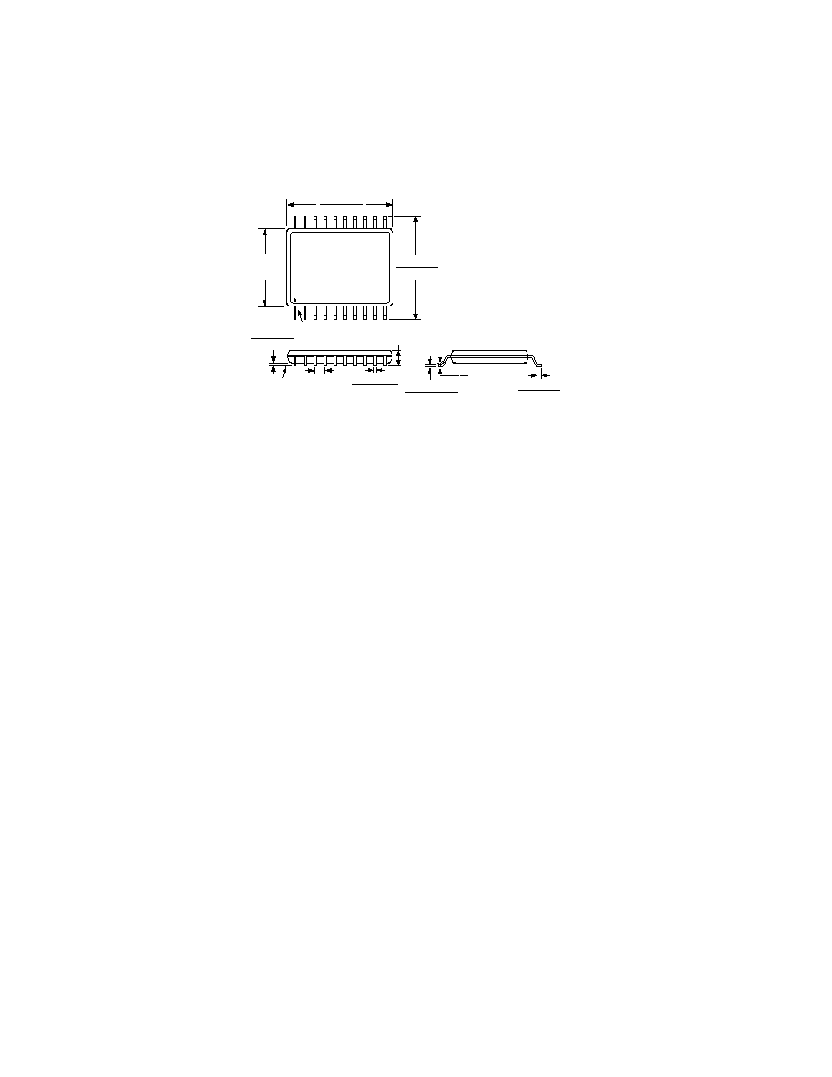
20-Lead Thin Shrink Small Outline (TSSOP)
RU-20
0.260 (6.60)
0.252 (6.40)
20
11
10
1
0.256 (6.50)
0.246 (6.25)
0.177 (4.50)
0.169 (4.30)
PIN 1
SEATING
PLANE
0.006 (0.15)
0.002 (0.05)
0.0118 (0.30)
0.0075 (0.19)
0.0256 (0.65)
BSC
0.0433 (1.10)
MAX
0.0079 (0.20)
0.0035 (0.090)
0.028 (0.70)
0.020 (0.50)
8
0
OUTLINE DIMENSIONS
Dimensions shown in inches and (mm).
C3579a≠2≠6/99
PRINTED IN U.S.A.