 | ÐлекÑÑоннÑй компоненÑ: ADM1175 | СкаÑаÑÑ:  PDF PDF  ZIP ZIP |
Äîêóìåíòàöèÿ è îïèñàíèÿ www.docs.chipfind.ru
Hot Swap Controller and
Digital Power Monitor with Convert Pin
ADM1175
Rev. 0
Information furnished by Analog Devices is believed to be accurate and reliable. However, no
responsibility is assumed by Analog Devices for its use, nor for any infringements of patents or other
rights of third parties that may result from its use. Specifications subject to change without notice. No
license is granted by implication or otherwise under any patent or patent rights of Analog Devices.
Trademarks and registered trademarks are the property of their respective owners.
One Technology Way, P.O. Box 9106, Norwood, MA 02062-9106, U.S.A.
Tel: 781.329.4700
www.analog.com
Fax: 781.461.3113
©2006 Analog Devices, Inc. All rights reserved.
FEATURES
Allows safe board insertion and removal from a live backplane
Controls supply voltages from 3.15 V to 16.5 V
Precision current sense amplifier
Precision voltage input
12-bit ADC for current and voltage readback
Charge pumped gate drive for external N-channel FET
Adjustable analog current limit with circuit breaker
±3% accurate hot swap current limit level
Fast response limits peak fault current
Automatic retry or latch-off on current fault
Programmable hot swap timing via TIMER pin
Active-high and active-low ON/ONB pin options
Convert start pin (CONV)
I
2
C® fast mode-compliant interface (400 kHz maximum)
10-lead MSOP
APPLICATIONS
Power monitoring/power budgeting
Central office equipment
Telecommunication and data communication equipment
PCs/servers
GENERAL DESCRIPTION
The ADM1175 is an integrated hot swap controller and current
sense amplifier that offers digital current and voltage monitoring
via an on-chip, 12-bit analog-to-digital converter (ADC),
communicated through an I
2
C interface.
An internal current sense amplifier senses voltage across the sense
resistor in the power path via the VCC pin and the SENSE pin.
The ADM1175 limits the current through this resistor by control-
ling the gate voltage of an external N-channel FET in the power
path, via the GATE pin. The sense voltage (and, therefore, the
inrush current) is kept below a preset maximum.
The ADM1175 protects the external FET by limiting the time
that it spends with maximum current running through it. This
current limit period is set by the choice of capacitor attached to
the TIMER pin. Additionally, the device provides protection from
overcurrent events that may occur once the hot swap event is
complete. In the case of a short-circuit event, the current in the
sense resistor exceeds an overcurrent trip threshold, and the
FET is switched off immediately by pulling down the GATE pin.
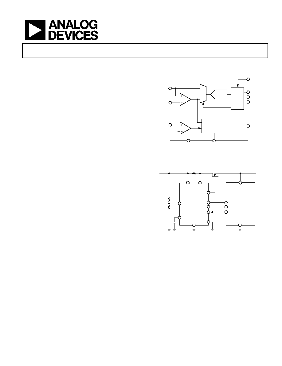
FUNCTIONAL BLOCK DIAGRAM
V
I
0
1
ADM1175-1
SENSE
ON
VCC
CONV
1.3V
MUX
I
2
C
12-BIT
ADC
FET DRIVE
CONTROLLER
GND
CURRENT
SENSE
AMPLIFIER
UV COMPARATOR
A
SDA
SCL
ADR
GATE
TIMER
05
64
7-
0
01
Figure 1.
R
SENSE
N-CHANNEL FET
P = VI
CONTROLLER
ADM1175-1
SENSE
VCC
SDA
SCL
SDA
SCL
GND
GATE
CONV
CONV
ADR
TIMER
3.15V TO 16.5V
ON
05
64
7-
0
02
Figure 2. Applications Diagram
A 12-bit ADC can measure the current seen in the sense resistor,
as well as the supply voltage on the VCC pin. An industry-standard
I
2
C interface allows a controller to read current and voltage data
from the ADC. Measurements can be initiated by an I
2
C command
or via the convert (CONV) pin. The CONV pin is especially
useful for synchronizing reads on multiple ADM1175 devices.
Alternatively, the ADC can run continuously, and the user can
read the latest conversion data whenever it is required. Up to four
unique I
2
C addresses can be created, depending on the way the
ADR pin is connected.
The ADM1175 is packaged in a 10-lead MSOP.

ADM1175
Rev. 0 | Page 2 of 24
TABLE OF CONTENTS
Features .............................................................................................. 1
Applications....................................................................................... 1
General Description ......................................................................... 1
Functional Block Diagram .............................................................. 1
Revision History ............................................................................... 2
Specifications..................................................................................... 3
Absolute Maximum Ratings............................................................ 6
ESD Caution.................................................................................. 6
Pin Configuration and Function Descriptions............................. 7
Typical Performance Characteristics ............................................. 8
Overview of the Hot Swap Function............................................ 13
Undervoltage Lockout ............................................................... 13
ON/ONB Function..................................................................... 13
TIMER Function ........................................................................ 13
GATE and TIMER Functions During a Hot Swap ................ 14
Calculating Current Limits and Fault Current Limit Time .. 14
Initial Timing Cycle ................................................................... 14
Hot Swap Retry Cycle on the ADM1175-1 and the
ADM1175-3 ................................................................................ 15
Voltage and Current Readback ..................................................... 16
Serial Bus Interface..................................................................... 16
Identifying the ADM1175 on the I
2
C Bus............................... 16
General I
2
C Timing.................................................................... 16
Write and Read Operations ...................................................... 18
Quick Command........................................................................ 18
Write Command Byte ................................................................ 18
Write Extended Byte .................................................................. 19
Read Voltage and/or Current Data Bytes ................................ 20
Applications Waveforms................................................................ 22
Kelvin Sense Resistor Connection ........................................... 23
Outline Dimensions ....................................................................... 24
Ordering Guide .......................................................................... 24
REVISION HISTORY
9/06--Revision 0: Initial Version

ADM1175
Rev. 0 | Page 3 of 24
SPECIFICATIONS
V
CC
= 3.15 V to 16.5 V; T
A
= -40°C to +85°C; typical values at T
A
= 25°C, unless otherwise noted.
Table 1.
Parameter Min
Typ
Max
Unit
Conditions
VCC PIN
Operating Voltage Range, V
VCC
3.15
16.5
V
Supply Current, I
CC
1.7
2.5
mA
Undervoltage Lockout, V
UVLO
2.8
V
V
CC
rising
Undervoltage Lockout Hysteresis, V
UVLOHYST
80
mV
ON/ONB PIN
Input Current, I
INON
-100
+100
nA
ON/ONB < 1.5 V
-2
+2
A
Rising Threshold, V
ONTH
1.26
1.3
1.34 V
ON/ONB rising
Trip Threshold Hysteresis, V
ONHYST
35
50
65 mV
Glitch Filter Time
3
s
CONV PIN
Input Current, I
INCONV
-1
+1
A
V
CONV(MAX)
= 3.6 V
Trip Threshold Low, V
CONVL
1.2 V
Trip Threshold High, V
CONVH
1.4
V
SENSE PIN
Input Leakage, I
SENSE
-1
+1
A
V
SENSE
= V
VCC
Overcurrent Fault Timing Threshold, V
OCTIM
92
mV
V
OCTRIM
= (V
VCC
- V
SENSE
), fault timing starts on the
TIMER pin
Overcurrent Limit Threshold, V
LIM
97
100
103
mV
V
LIM
= (V
VCC
- V
SENSE
), closed-loop regulation to
a current limit
Fast Overcurrent Trip Threshold, V
OCFAST
115
mV
V
OCFAST
= (V
VCC
- V
SENSE
), gate pull-down current
turned on
GATE PIN
Drive Voltage, V
GATE
3
6 9 V
V
GATE
- V
VCC
, V
VCC
= 3.15 V
9
11
13
V
V
GATE
- V
VCC
, V
VCC
= 5 V
7
10 13 V
V
GATE
- V
VCC
, V
VCC
= 16.5 V
Pull-Up Current
8
12.5
17
A
V
GATE
= 0 V
Pull-Down Current
1.5
mA
V
GATE
= 3 V, V
VCC
= 3.15 V
5
mA
V
GATE
= 3 V, V
VCC
= 5 V
7
mA
V
GATE
= 3 V, V
VCC
= 16.5 V
TIMER PIN
Pull-Up Current (Power On Reset), I
TIMERUPPOR
-3.5
-5
-6.5
A
Initial cycle, V
TIMER
= 1 V
Pull-Up Current (Fault Mode), I
TIMERUPFAULT
-40
-60
-80
A
During current fault, V
TIMER
= 1 V
Pull-Down Current (Retry Mode), I
TIMERDNRETRY
2
3
A
After current fault and during a cool-down
period on a retry device, V
TIMER
= 1 V
Pull-Down Current, I
TIMERDN
100
A
Normal operation, V
TIMER
= 1 V
Trip Threshold High, V
TIMERH
1.26
1.3
1.34
V
TIMER rising
Trip Threshold Low, V
TIMERL
0.175
0.2
0.225
V
TIMER falling
ADR PIN
Set Address to 00, V
ADRLOWV
0
0.8
V
Low state
Set Address to 01, R
ADRLOWZ
135
150
165
k
Resistor to ground state, load pin with specified
resistance for 01 decode
Set Address to 10, I
ADRHIGHZ
-1
+1
A
Open state, maximum load allowed on ADR pin
for 10 decode
Set Address to 11, V
ADRHIGHV
2
5.5
V
High state
Input Current for 11 Decode, I
ADRLOW
3
10
A
V
ADR
= 2.0 V to 5.5 V
Input Current for 00 Decode, I
ADRHIGH
-40
-22
A
V
ADR
= 0 V to 0.8 V

ADM1175
Rev. 0 | Page 4 of 24
Parameter Min
Typ
Max
Unit
Conditions
MONITORING ACCURACY
1
Current Sense Absolute Accuracy
-1.45
+1.45 %
V
SENSE
= 75 mV
0°C to +70°C
-1.8
+1.8
%
V
SENSE
= 50 mV
0°C to +70°C
-2.8
+2.8 %
V
SENSE
= 25 mV
0°C to +70°C
-5.7
+5.7
%
V
SENSE
= 12.5 mV
0°C to +70°C
-1.5
+1.5 %
V
SENSE
= 75 mV
0°C to +85°C
-1.8
+1.8 %
V
SENSE
= 50 mV
0°C to +85°C
-2.95
+2.95 %
V
SENSE
= 25 mV
0°C to +85°C
-6.1
+6.1 %
V
SENSE
= 12.5 mV
0°C to +85°C
-1.95
+1.95 %
V
SENSE
= 75 mV
-40°C to +85°C
-2.45
+2.45 %
V
SENSE
= 50 mV
-40°C to +85°C
-3.85
+3.85 %
V
SENSE
= 25 mV
-40°C to +85°C
-6.7
+6.7 %
V
SENSE
= 12.5 mV
-40°C to +85°C
V
SENSE
for ADC Full Scale
105.84
mV
This is an absolute value to be used when
converting ADC codes to current readings;
any inaccuracy in this value is factored into
absolute current accuracy values (see specs
for Current Sense Absolute Accuracy)
Voltage Accuracy
-0.85
+0.85
%
V
CC
= 3 V minimum
(low range)
0°C to +70°C
-0.9
+0.9
%
V
CC
= 6 V minimum
(high range)
0°C to +70°C
-0.85
+0.85
%
V
CC
= 3 V minimum
(low range)
0°C to +85°C
-0.9
+0.9
%
V
CC
= 6 V minimum
(high range)
0°C to +85°C
-0.9
+0.9
%
V
CC
= 3 V minimum
(low range)
-40°C to +85°C
-1.15
+1.15
%
V
CC
= 6 V minimum
(high range)
-40°C to +85°C
V
CC
for ADC Full Scale,
Low Range (VRANGE = 1)
6.65
V
V
CC
for ADC Full Scale,
High Range (VRANGE = 0)
26.35
V
These are absolute values to be used when
converting ADC codes to voltage readings;
any inaccuracy in these values is factored into
voltage accuracy values (see specs for Voltage
Accuracy)
I
2
C TIMING
Low Level Input Voltage, V
IL
0.3
V
BUS
V
High Level Input Voltage, V
IH
0.7 V
BUS
V
Low Level Output Voltage on SDA, V
OL
0.4
V
I
OL
= 3 mA
Output Fall Time on SDA from V
IHMIN
to V
ILMAX
20 +
0.1 C
B
250
ns
C
B
= bus capacitance from SDA to GND
Maximum Width of Spikes Suppressed by
Input Filtering on SDA and SCL Pins
50
250
ns
Input Current, I
I
, on SDA/SCL When Not
Driving Out a Logic Low
-10
+10 A
Input Capacitance on SDA/SCL
5
pF
SCL Clock Frequency, f
SCL
400
kHz
Low Period of the SCL Clock
600
ns
High Period of the SCL Clock
1300
ns

ADM1175
Rev. 0 | Page 5 of 24
Parameter Min
Typ
Max
Unit
Conditions
Setup Time for a Repeated Start Condition,
t
SU;STA
600
ns
SDA Output Data Hold Time, t
HD;DAT
100
900 ns
Setup Time for a Stop Condition, t
SU;STO
600
ns
Bus Free Time Between a Stop and a Start
Condition, t
BUF
1300
ns
Capacitive Load for Each Bus Line
400
pF
1
Monitoring accuracy is a measure of the error in a code that is read back for a particular voltage/current. This is a combination of amplifier error, reference error,
ADC error, and error in ADC full-scale code conversion factor.
ADM1175
Rev. 0 | Page 6 of 24
ABSOLUTE MAXIMUM RATINGS
Table 2.
Parameter Rating
VCC Pin
20 V
SENSE Pin
20 V
TIMER Pin
-0.3 V to +6 V
ON/ONB Pin
-0.3 V to +20 V
CONV Pin
-0.3 V to +6 V
GATE Pin
30 V
SDA Pin, SCL Pin
-0.3 V to +7 V
ADR Pin
-0.3 V to +6 V
Storage Temperature Range
-65°C to +125°C
Operating Temperature Range
-40°C to +85°C
Lead Temperature (Soldering
, 10 sec)
300°C
Junction Temperature
150°C
Stresses above those listed under Absolute Maximum Ratings
may cause permanent damage to the device. This is a stress
rating only; functional operation of the device at these or any
other conditions above those indicated in the operational
section of this specification is not implied. Exposure to absolute
maximum rating conditions for extended periods may affect
device reliability.
Table 3. Thermal Resistance
Package Type
JA
Unit
10-Lead MSOP
137.5
°C/W
ESD CAUTION

ADM1175
Rev. 0 | Page 7 of 24
PIN CONFIGURATION AND FUNCTION DESCRIPTIONS
VCC
1
SENSE
2
ON/ONB
3
GND
4
TIMER
5
GATE
10
CONV
9
ADR
8
SDA
7
SCL
6
ADM1175
TOP VIEW
(Not to Scale)
05
64
7-
0
0
3
Figure 3. Pin Configuration
Table 4. Pin Function Descriptions
Pin No.
Mnemonic
Description
1 VCC
Positive Supply Input Pin. The operating supply voltage range is from 3.15 V to 16.5 V. An undervoltage
lockout (UVLO) circuit resets the ADM1175 when a low supply voltage is detected.
2 SENSE
Current Sense Input Pin. A sense resistor between the VCC pin and the SENSE pin sets the analog current
limit. The hot swap operation of the ADM1175 controls the external FET gate to maintain the (V
VCC
- V
SENSE
)
voltage at 100 mV or below.
3 ON/ONB Undervoltage or Overvoltage Input Pin. This pin is active high on the ADM1175-1 and ADM1175-2 and
active-low on the ADM1175-3 and ADM1175-4. An internal ON comparator has a trip threshold of 1.3 V,
and the output of this comparator is used as an enable for the hot swap operation. For the ON pin variants
with an external resistor divider from VCC to GND, this pin can be used to enable the hot swap operation
on a specific voltage on VCC, giving an undervoltage function. Similarly, for the ONB pin variants, an external
resistor divider can be used to create an overvoltage function, where the divider sets a voltage on VCC at
which the hot swap operation is switched off, pulling the GATE to ground.
4
GND
Chip Ground Pin.
5 TIMER
Timer Pin. An external capacitor, C
TIMER
, sets a 270 ms/F initial timing cycle delay and a 21.7 ms/F fault delay.
The GATE pin turns off when the TIMER pin is pulled beyond the upper threshold. An overvoltage detection
with an external Zener can be used to force this pin high.
6 SCL
I
2
C Clock Pin. Open-drain input requires an external resistive pull-up.
7 SDA
I
2
C Data I/O Pin. Open-drain input/output. Requires an external resistive pull-up.
8 ADR
I
2
C Address Pin. This pin can be tied low, tied high, left floating, or tied low through a resistor to set four
different I
2
C addresses.
9 CONV
Convert Start Pin. A high level on this pin enables an ADC conversion. The state of an internal control register,
which is set through the I
2
C interface, configures the part to convert current only, voltage only, or both
channels when the convert pin is asserted.
10 GATE
GATE Output Pin. This pin is the high-side gate drive of an external N-channel FET. This pin is driven by the
FET drive controller, which utilizes a charge pump to provide a 12.5 A pull-up current to charge the FET
GATE pin. The FET drive controller regulates to a maximum load current (100 mV through the sense resistor)
by modulating the GATE pin.
ADM1175
Rev. 0 | Page 8 of 24
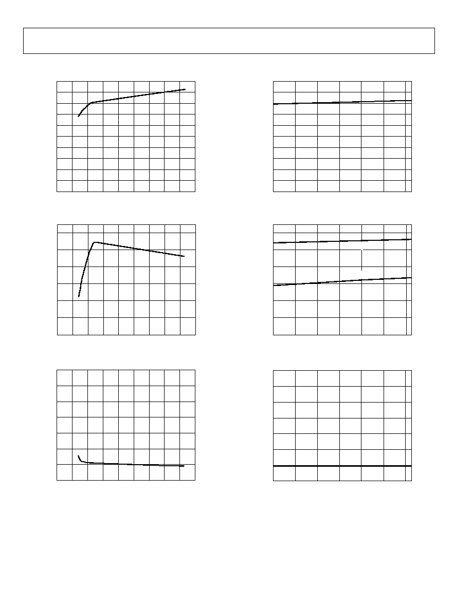
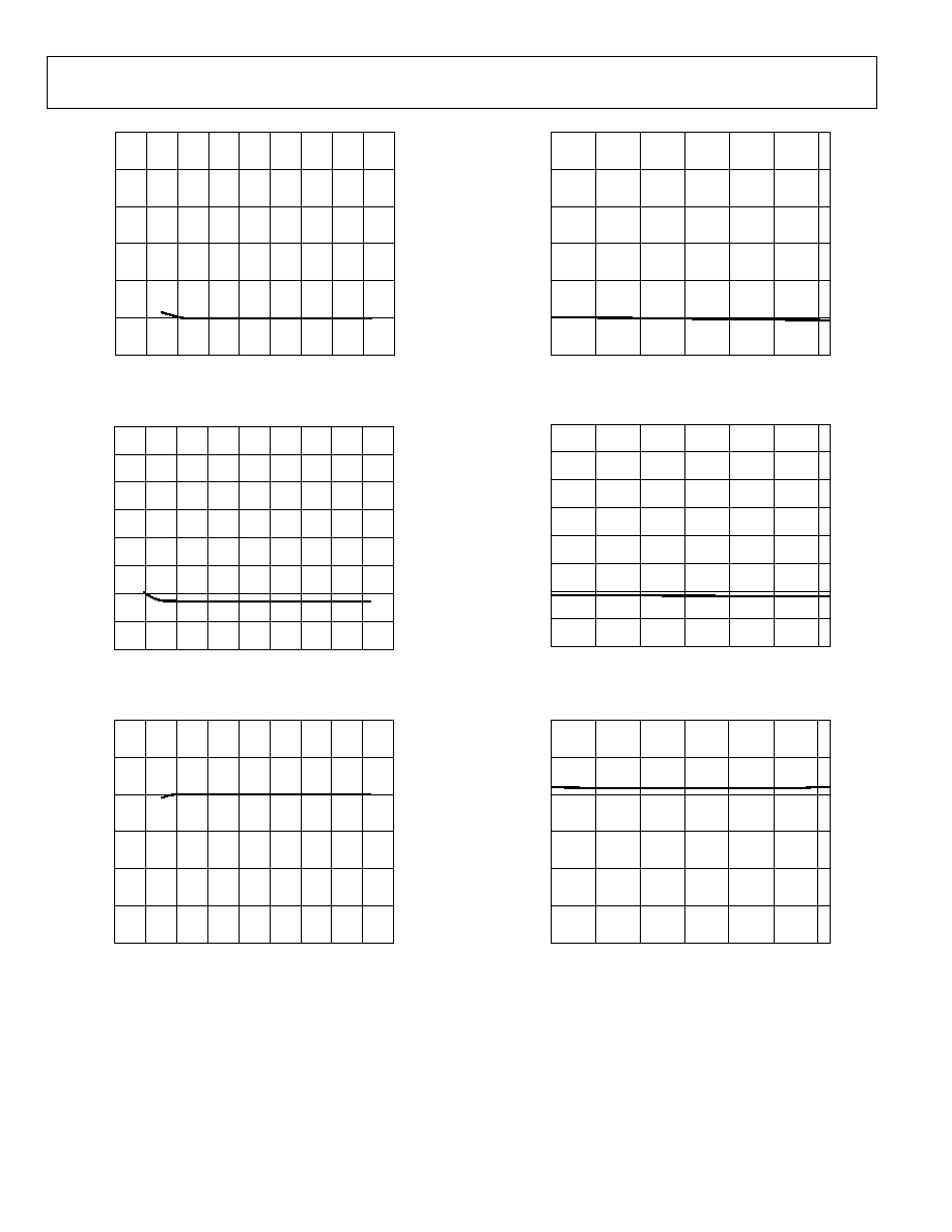
TYPICAL PERFORMANCE CHARACTERISTICS
05
64
7-
0
21
2.0
1.8
1.6
1.4
1.2
1.0
0.8
0.6
0.4
0.2
0
0
2
4
6
8
10
14
1
12
16
I
CC
(m
A
)
V
CC
(V)
8
Figure 4. Supply Current vs. Supply Voltage
12
10
8
6
4
2
0
0
18
16
14
12
10
8
6
4
2
D
R
I
VE VO
L
T
A
G
E
(V
)
V
CC
(V)
05
64
7-
0
29
10
12
16
14
8
6
4
2
I
GA
T
E
(µ
A
)
V
CC
(V)
Figure 5. Drive Voltage (V
GATE
- V
CC
) vs. Supply Voltage
0
14
12
10
8
6
4
2
0
18
05
64
7-
0
27
Figure 6. Gate Pull-Up Current vs. Supply Voltage
2.0
1.8
1.6
1.4
1.2
1.0
0.8
0.6
0.4
0.2
0
40
80
60
40
20
0
20
I
CC
(m
A
)
TEMPERATURE (°C)
05
64
7-
02
2
Figure 7. Supply Current vs. Temperature (Gate On)
12
10
8
6
4
2
0
40
80
60
40
20
0
20
DR
I
V
E
V
O
L
T
AG
E
(
V
)
TEMPERATURE (°C)
5V V
CC
3.15V V
CC
05
64
7-
03
0
0
2
4
6
8
10
12
14
40
80
60
40
20
0
20
I
GA
T
E
(µ
A
)
TEMPERATURE (°C)
Figure 8. Drive Voltage (V
GATE
- V
CC
) vs. Temperature
05
64
7-
02
8
Figure 9. Gate Pull-Up Current vs. Temperature
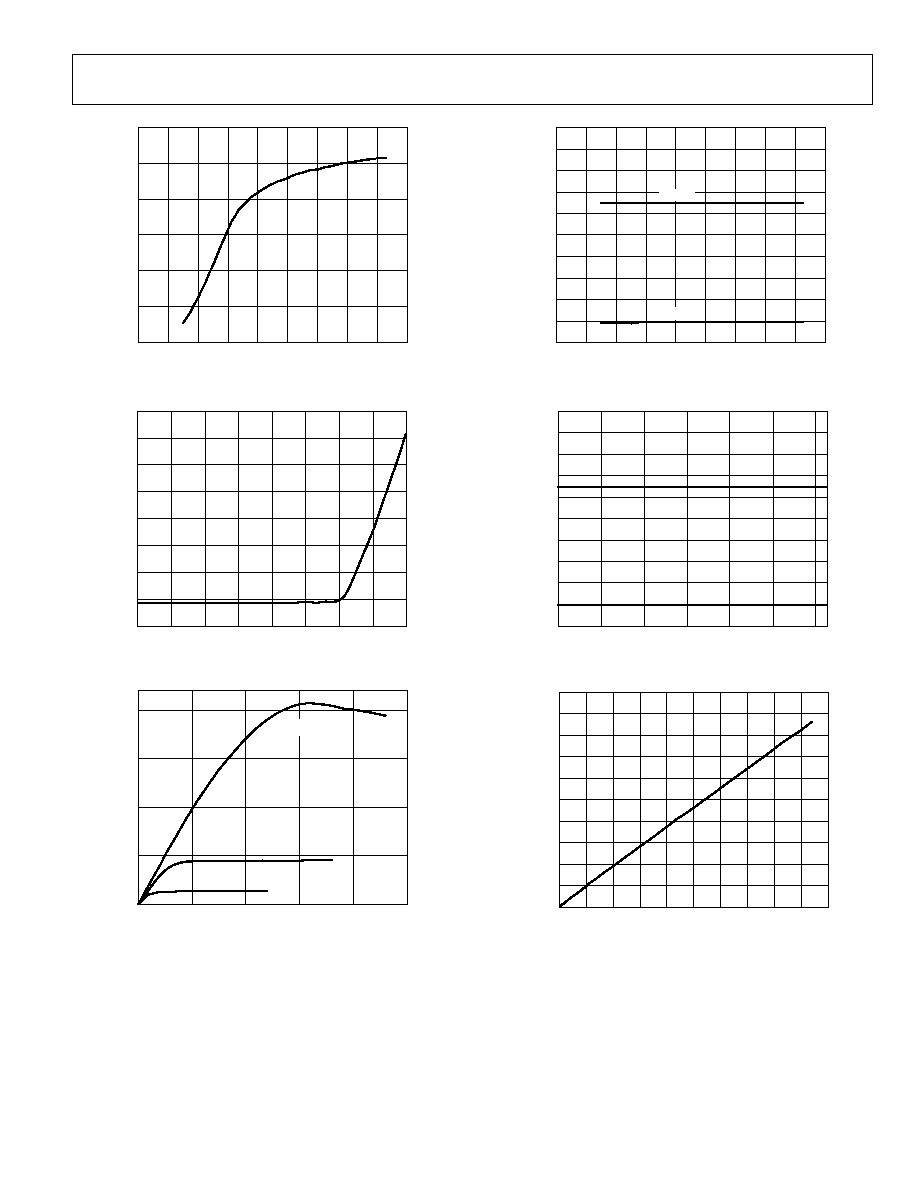
ADM1175
Rev. 0 | Page 9 of 24
16
14
12
10
8
6
4
2
I
GA
T
E
(m
A
)
V
CC
(V)
12
10
8
6
4
2
0
0
18
05
64
7-
0
38
2.0
1.8
1.6
1.4
1.2
1.0
0.8
0.6
0.4
0.2
0
T
I
M
E
R T
H
RE
S
H
O
L
D (
V
)
V
CC
(V)
05
64
7-
0
31
14
12
10
8
6
4
2
I
GA
T
E
(µ
A
)
V
GATE
(V)
0
18
10
12
16
14
8
6
4
2
Figure 10. Gate Pull-Down Current vs. V
CC
at V
GATE
= 5 V
2
14
12
10
8
6
4
2
0
0
16
HIGH
LOW
2.0
1.8
1.6
1.4
1.2
1.0
0.8
0.6
0.4
0.2
0
40
80
HIGH
LOW
60
40
20
0
20
T
I
M
E
R HI
G
H T
HR
E
S
H
O
L
D (
V
)
TEMPERATURE (°C)
05
64
7-
0
40
20
15
10
5
I
GA
T
E
(m
A
)
V
GATE
(V)
Figure 11. Gate Pull-Up Current vs. Gate Voltage at V
CC
= 5 V
0
5
10
15
20
0
25
V
CC
= 3V
V
CC
= 5V
V
CC
= 12V
05
64
7-
0
43
Figure 12. Gate Pull-Down Current vs. Gate Voltage
Figure 13. Timer Threshold vs. Supply Voltage
05
64
7-
03
9
0
100
80
60
40
20
90
70
50
30
10
0
5.0
4.5
4.0
3.5
3.0
2.5
2.0
1.5
1.0
0.5
GA
T
E
ON
T
IM
E
(
m
s
)
C
TIMER
(µF)
05
64
7-
0
50
Figure 14. Timer Threshold vs. Temperature
Figure 15. Current Limit On Time vs. Timer Capacitance
ADM1175
Rev. 0 | Page 10 of 24
0
18
10
12
16
14
8
6
4
2
0
1
2
3
4
5
6
I
TI
M
E
R
(µ
A
)
V
CC
(V)
05
64
7-
0
32
Figure 16.Timer Pull-Up Current (Initial Cycle) vs. Supply Voltage
0
80
70
60
50
40
30
20
10
I
TI
M
E
R
(µ
A
)
V
CC
(V)
05
64
7-
0
34
0
18
10
12
16
14
8
6
4
2
Figure 17. Timer Pull-Up Current (C. B. Delay) vs. Supply Voltage
3.0
2.5
2.0
1.5
1.0
0.5
0
I
TI
M
E
R
(µ
A
)
V
CC
(V)
05
64
7-
0
36
0
18
10
12
16
14
8
6
4
2
Figure 18. Timer Pull-Down Current (Cool-Off Cycle) vs. Supply Voltage
0
1
2
3
4
5
6
40
80
60
40
20
0
20
I
TI
M
E
R
(µ
A
)
TEMPERATURE (°C)
05
64
7-
03
3
Figure 19. Timer Pull-Up Current (Initial Cycle) vs. Temperature
0
10
20
30
40
50
80
70
60
40
80
60
40
20
0
20
I
TI
M
E
R
(µ
A
)
TEMPERATURE (°C)
05
64
7-
03
5
Figure 20. Timer Pull-Up Current (C. B. Delay) vs. Temperature
3.0
2.5
2.0
1.5
1.0
0.5
0
40
80
60
40
20
0
20
I
TI
M
E
R
(µ
A
)
TEMPERATURE (°C)
05
64
7-
03
7
Figure 21. Timer Pull-Down Current (Cool-Off Cycle) vs. Temperature
ADM1175
Rev. 0 | Page 11 of 24
120
80
85
90
95
100
105
110
115
2
18
16
14
12
10
8
6
4
V
LI
M
(m
V
)
V
CC
(V)
05
64
7-
0
41
Figure 22. Circuit Breaker Limit Voltage vs. Supply Voltage
110
90
92
94
96
98
100
102
104
106
108
40
80
60
40
20
0
20
V (
m
V
)
TEMPERATURE (°C)
V
OCTIM
V
LIM
V
OCFAST
05
64
7-
04
2
Figure 23. V
OCTIM
, V
LIM
, V
OCFAST
vs. Temperature
05
64
7-
02
6
3.2
3.0
2.8
2.6
2.4
2.2
2.0
1.8
1.6
1.4
1.2
1.0
0.8
0.6
0.4
0.2
0
35
30
25
20
15
10
5
0
5
10
V
AD
R
I
ADR
(µA)
11 DECODE
10 DECODE
01 DECODE 00 DECODE
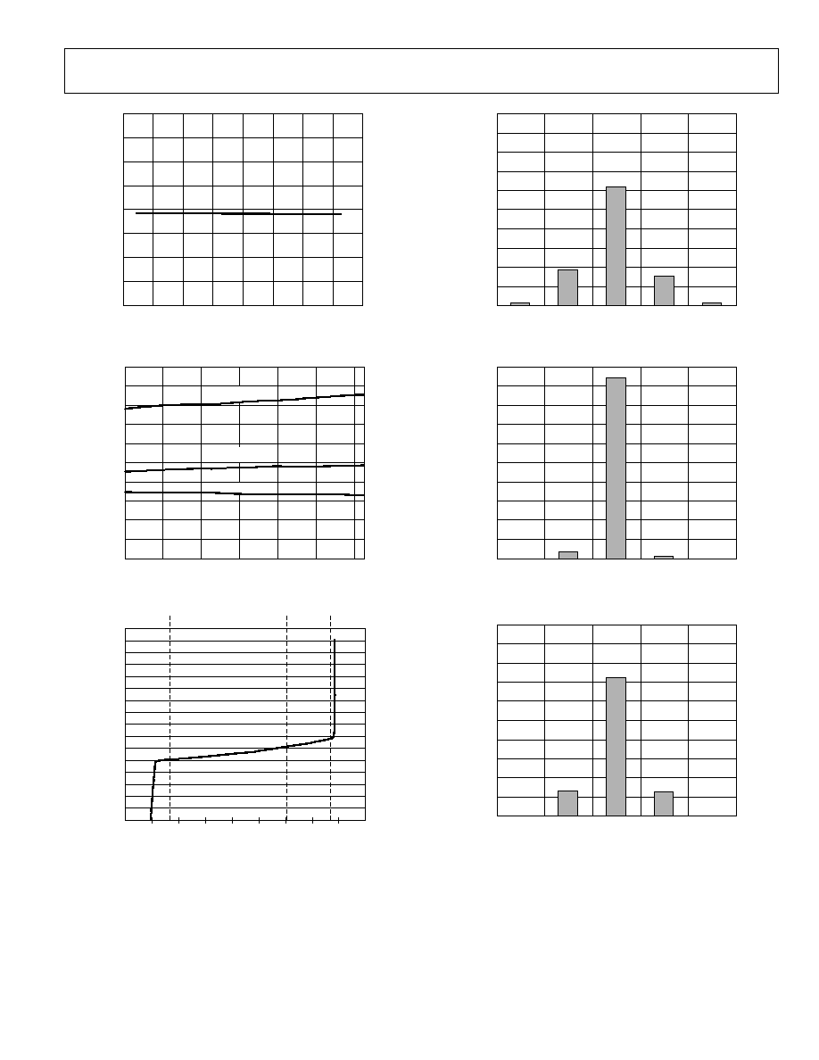
Figure 24. Address Pin Voltage vs. Address Pin Current
for Four Addressing Options
0
1000
900
800
700
600
500
400
300
200
100
HI
T
S
P
E
R
CO
DE
(
1000 R
E
ADS
)
CODE
05
64
7-
0
60
2047
2048
2049
2050
2046
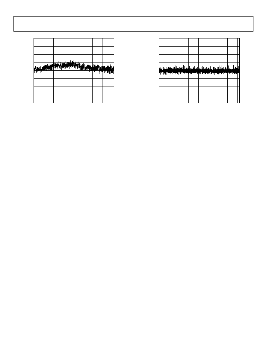
Figure 25. ADC Noise, Current Channel, Midcode Input, 1000 Reads
0
1000
900
800
700
600
500
400
300
200
100
HI
T
S
P
E
R
CO
DE
(
1000 R
E
ADS
)
CODE
05
64
7-
0
61
780
781
782
783
779
Figure 26. ADC Noise, 14:1 Voltage Channel, 5 V Input, 1000 Reads
0
1000
900
800
700
600
500
400
300
200
100
HI
T
S
P
E
R CO
DE
(
1000
R
E
ADS
)
CODE
05
64
7-
0
62
3079
3080
3081
3082
3078
Figure 27. ADC Noise, 7:1 Voltage Channel, 5 V Input, 1000 Reads
ADM1175
Rev. 0 | Page 12 of 24
4
3
2
1
0
1
2
3
4
0
4000
2500
3000
3500
2000
1500
1000
500
IN
L (
L
S
B
)
CODE
05
64
7-
02
3
Figure 28. INL for ADC
4
3
2
1
0
1
2
3
4
0
4000
2500
3000
3500
2000
1500
1000
500
DN
L
(
L
S
B
)
CODE
05
64
7-
02
4
Figure 29. DNL for ADC

ADM1175
Rev. 0 | Page 13 of 24
OVERVIEW OF THE HOT SWAP FUNCTION
When circuit boards are inserted into a live backplane, discharged
supply bypass capacitors draw large transient currents from the
backplane power bus as they charge. Such transient currents can
cause permanent damage to connector pins, as well as dips on
the backplane supply that can reset other boards in the system.
The ADM1175 is designed to turn a circuit board supply voltage
on and off in a controlled manner, allowing the circuit board to
be safely inserted into or removed from a live backplane. The
ADM1175 can reside either on the backplane or on the circuit
board itself.
The ADM1175 controls the inrush current to a fixed maximum
level by modulating the gate of an external N-channel FET placed
between the live supply rail and the load. This hot swap function
protects the card connectors and the FET itself from damage
and limits any problems that can be caused by high current loads
on the live supply rail.
The ADM1175 holds the GATE pin down (and, thus, the FET is
held off) until a number of conditions are met. An undervoltage
lockout circuit ensures that the device is provided with an adequate
input supply voltage. Once the input supply voltage has been
successfully detected, the device goes through an initial timing
cycle to provide a delay before it attempts to hot swap. This delay
ensures that the board is fully seated in the backplane before the
board is powered up.
Once the initial timing cycle is complete, the hot swap function
is switched on under control of the ON/ONB pin. When ON/ONB
is asserted (high for the ADM1175-1 and ADM1175-2, low for
the ADM1175-3 and ADM1175-4), the hot swap operation starts.
The ADM1175 charges up the gate of the FET to turn on the
load. It continues to charge up the GATE pin until the linear
current limit (set to 100 mV/R
SENSE
) is reached. For some combi-
nations of low load capacitance and high current limit, this limit
may not be reached before the load is fully charged up. If current
limit is reached, the ADM1175 regulates the GATE pin to keep
the current at this limit. For currents above the overcurrent fault
timing threshold, nominally 100 mV/R
SENSE
, the current fault is
timed by sourcing a current out to the TIMER pin. If the load
becomes fully charged before the fault current limit time is
reached (when the TIMER pin reaches 1.3 V), the current drops
below the overcurrent fault timing threshold. The ADM1175
then charges the GATE pin higher to fully enhance the FET for
lowest R
ON
, and the TIMER pin is pulled down again.
If the fault current limit time is reached before the load drops
below the current limit, a fault has been detected, and the hot
swap operation is aborted by pulling down on the GATE pin to
turn off the FET. The ADM1175-2 and ADM1175-4 are latched
off. They attempt to hot swap again only when the ON/ONB pin is
deasserted and then asserted again.
The ADM1175-1 and ADM1175-3 retry the hot swap operation
indefinitely, keeping the FET in its safe operating area (SOA) by
using the TIMER pin to time a cool-down period in between
hot swap attempts. The current and voltage threshold combinations
on the TIMER pin set the retry duty cycle to 3.8%.
The ADM1175 is designed to operate over a range of supplies
from 3.15 V to 16.5 V.
UNDERVOLTAGE LOCKOUT
An internal undervoltage lockout (UVLO) circuit resets the
ADM1175 if the VCC
supply is too low for normal operation.
The UVLO has a low-to-high threshold of 2.8 V, with 80 mV
hysteresis. Above 2.8 V supply voltage, the ADM1175 starts the
initial timing cycle.
ON/ONB FUNCTION
The ADM1175-1 and ADM1175-2 have an active high ON pin.
The ON pin is the input to a comparator that has a low-to-high
threshold of 1.3 V, a 50 mV hysteresis, and a glitch filter of 3 s.
A low input on the ON pin turns off the hot swap operation by
pulling the GATE pin to ground, turning off the external FET.
The TIMER pin is also reset by turning on a pull-down current
on this pin. A low-to-high transition on the ON pin starts the
hot swap operation. A 10 k pull-up resistor connecting the
ON pin to the supply is recommended.
Alternatively, an external resistor divider at the ON pin can be
used to program an undervoltage lockout value higher than the
internal UVLO circuit, thereby setting a voltage level at the
VCC supply, where the hot swap operation is to start. An RC
filter can be added at the ON pin to increase the delay time at
card insertion if the initial timing cycle delay is insufficient.
The ADM1175-3 and ADM1175-4 have an active low ONB pin.
This pin operates exactly as described above for the ON pin,
but the polarity is reversed. This allows this pin to function as
an overvoltage detector that can use the external FET as a circuit
breaker for overvoltage conditions on the monitored supply.
TIMER FUNCTION
The TIMER pin handles several timing functions with an
external capacitor, C
TIMER
. There are two comparator thresholds:
V
TIMERH
(0.2 V) and V
TIMERL
(1.3 V). The four timing current
sources are a 5 A pull-up, a 60 A pull-up, a 2 A pull-down,
and a 100 A pull-down. The 100 A pull-down is a non-ideal
current source, approximating a 7 k resistor below 0.4 V.
These current and voltage levels, together with the value of C
TIMER
chosen by the user, determine the initial timing cycle time, the
fault current limit time, and the hot swap retry duty cycle.

ADM1175
Rev. 0 | Page 14 of 24
GATE AND TIMER FUNCTIONS
DURING A HOT SWAP
During hot insertion of a board onto a live supply rail at VCC,
the abrupt application of supply voltage charges the external FET
drain/gate capacitance, which can cause an unwanted gate voltage
spike. An internal circuit holds GATE low before the internal
circuitry wakes up. This reduces the FET current surges substan-
tially at insertion. The GATE pin is also held low during the
initial timing cycle and until the ON pin has been taken high
to start the hot swap operation.
During hot swap operation, the GATE pin is first pulled up by
a 12 A current source. If the current through the sense resistor
reaches the overcurrent fault timing threshold, V
OCTIM
, a pull-up
current of 60 A on the TIMER pin, is turned on, and this pin
starts charging up. At a slightly higher voltage in the sense resistor,
the error amplifier servos the GATE pin to maintain a constant
current to the load by controlling the voltage across the sense
resistor to the linear current limit, V
LIM
.
A normal hot swap is complete when the board supply capaci-
tors near full charge, and the current through the sense resistor
drops to eventually reach the level of the board load current.
As soon as the current drops below the overcurrent fault timing
threshold, the current into the TIMER pin switches from being
a 60 A pull-up to a 100 A pull-down. The ADM1175 then
drives the GATE voltage as high as it can to fully enhance the
FET and reduce R
ON
losses to a minimum.
A hot swap fails if the load current does not drop below the
overcurrent fault timing threshold, V
OCTIM
, before the TIMER
pin has charged up to 1.3 V. In this case, the GATE pin is then
pulled down with a 2 mA current sink. The GATE pull-down
stays on until a hot swap retry starts, which can be forced by
deasserting and then reasserting the ON/ONB pin. On the
ADM1175-1 and ADM1175-3, the device retries automatically
after a cool-down period.
The ADM1175 also features a method of protection from
sudden load current surges, such as a low impedance fault,
when the current seen across the sense resistor may go well
beyond the linear current limit. If the fast overcurrent trip
threshold, V
OCFAST
, is exceeded, the 2 mA GATE pull-down is
turned on immediately. This pulls the GATE voltage down
quickly to enable the ADM1175 to limit the length of the current
spike that gets through, and also to bring the current through
the sense resistor back into linear regulation as quickly as
possible. This process protects the backplane supply from
sustained overcurrent conditions that can otherwise cause the
backplane supply to droop during the overcurrent event.
CALCULATING CURRENT LIMITS AND
FAULT CURRENT LIMIT TIME
The nominal linear current limit is determined by a sense resistor
connected between the VCC pin and the SENSE pin, as given
by Equation 1.
I
LIMIT(NOM)
= V
LIM(NOM)
/R
SENSE
= 100 mV/R
SENSE
(1)
The minimum linear fault current is given by Equation 2.
I
LIMIT(MIN)
= V
LIM(MIN)
/R
SENSE(MAX)
= 90 mV/R
SENSE(MAX)
(2)
The maximum linear fault current is given by Equation 3.
I
LIMIT(MAX)
= V
LIM(MAX)
/R
SENSE(MIN)
= 110 mV/R
SENSE(MIN)
(3)
The power rating of the sense resistor should be rated at the
maximum linear fault current level.
The minimum overcurrent fault timing threshold current is
given by Equation 4.
I
OCTIM(MIN)
= V
OCTIM(MIN)
/R
SENSE(MAX)
= 85 mV/R
SENSE(MAX)
(4)
The maximum fast overcurrent trip threshold current is given by
Equation 5.
I
OCFAST(MAX)
= V
OCFAST(MAX)
/R
SENSE(MIN)
= 115 mV/R
SENSE(MIN)
(5)
The fault current limit time is the time that a device spends
timing an overcurrent fault, and is given by Equation 6.
t
FAULT
21.7 × C
TIMER
ms/F (6)
INITIAL TIMING CYCLE
When VCC is first connected to the backplane supply, the
internal supply (Time Point (1) in Figure 30) of the ADM1175
must be charged up. A very short time later (significantly less
than 1 ms), the internal supply is fully up and, because the
undervoltage lockout voltage has been exceeded at VCC, the
device comes out of reset. During this first short reset period,
the GATE pin is held down with a 25 mA pull-down current,
and the TIMER pin is pulled down with a 100 A current sink.
The ADM1175 then goes through an initial timing cycle. At
Time Point (2), the TIMER pin is pulled high with 5 A. At
Time Point (3), the TIMER reaches the V
TIMERL
threshold, and
the first portion of the initial cycle ends. The 100 A current
source then pulls down the TIMER pin until it reaches 0.2 V
at Time Point (4). The initial cycle delay (Time Point (2) to
Time Point (4)) is related to C
TIMER
by Equation 7.
t
INITIAL
270 × C
TIMER
ms/F
(7)
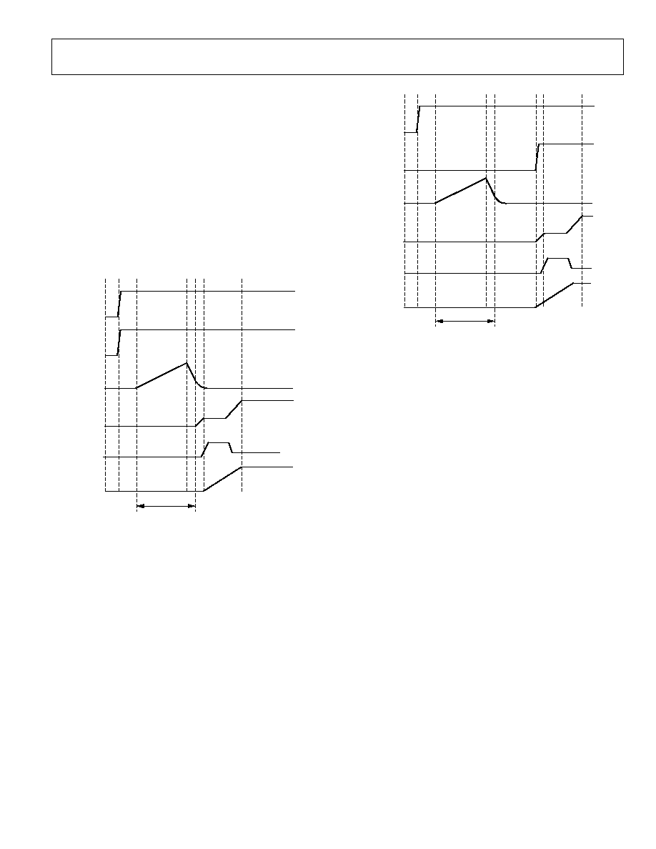
ADM1175
Rev. 0 | Page 15 of 24
When the initial timing cycle terminates, the device is ready to
start a hot swap operation (assuming the ON/ONB pin is asserted).
In the example shown in Figure 30, the ON pin is asserted at the
same time that V
CC
is applied, so the hot swap operation starts
immediately after Time Point (4). At this point, the FET gate is
charged up with a 12 A current source. At Time Point (5), the
threshold voltage of the FET is reached, and the load current
begins to flow. The FET is controlled to keep the sense voltage
at 100 mV (this corresponds to a maximum load current level
defined by the value of R
SENSE
). At Time Point (6), V
GATE
and
V
OUT
have reached their full potential, and the load current has
settled to its nominal level. Figure 31 illustrates the situation
where the ON pin is asserted after V
CC
is applied.
V
VCC
(1)
INITIAL TIMING
CYCLE
(2)
(3)(4) (5)
(6)
V
ON
V
TIMER
V
GATE
V
SENSE
V
OUT
05
64
7-
0
04
Figure 30. Startup (ON Asserts as Power Is Applied)
INITIAL TIMING
CYCLE
V
VCC
V
ON
V
TIMER
V
GATE
V
SENSE
V
OUT
(1)
(2)
(3)(4)
(5)(6)
(7)
05
64
7-
00
5
Figure 31. Startup (ON Asserts After Power Is Applied)
HOT SWAP RETRY CYCLE ON THE ADM1175-1
AND THE ADM1175-3
With the ADM1175-1 and the ADM1175-3, the device turns off
the FET after an overcurrent fault and then uses the TIMER pin
to time a delay before automatically retrying to hot swap.
As with all ADM1175 devices, on overcurrent fault is timed by
charging the TIMER cap with a 60 A pull-up current. When
the TIMER pin reaches 1.3 V, the fault current limit time has
been reached, and the GATE pin is pulled down. On the
ADM1175-1 and the ADM1175-3, the TIMER pin is then
pulled down with a 2 A current sink. When the TIMER pin
reaches 0.2 V, it automatically restarts the hot swap operation.
The cool-down period is related to C
TIMER
by Equation 8.
t
COOL
550 × C
TIMER
ms/F (8)
Thus, the retry duty cycle is given by Equation 9.
t
FAULT
/(t
COOL
+ t
FAULT
) × 100% = 3.8%
(9)

ADM1175
Rev. 0 | Page 16 of 24
VOLTAGE AND CURRENT READBACK
In addition to providing hot swap functionality, the ADM1175
also contains the components to allow voltage and current
readback over an Inter-IC (I
2
C) bus. The voltage output of the
current sense amplifier and the voltage on the VCC pin are fed
into a 12-bit ADC via a multiplexer. The device can be
instructed to convert voltage and/or current at any time during
operation via an I
2
C command or an assertion on the convert
start (CONV) pin. When all conversions are complete, the voltage
and/or current values can be read out to 12-bit accuracy in two
or three bytes.
SERIAL BUS INTERFACE
Control of the ADM1175 is carried out via the I
2
C bus. This
interface is compatible with I
2
C fast mode (400 kHz maximum).
The ADM1175 is connected to this bus as a slave device, under
the control of a master device.
IDENTIFYING THE ADM1175 ON THE I
2
C BUS
The ADM1175 has a 7-bit serial bus slave address. When the
device powers up, it does so with a default serial bus address. The
five MSBs of the address are set to 11010; the two LSBs are deter-
mined by the state of the ADR pin. There are four different
configurations available on the ADR pin that correspond to four
different I
2
C addresses for the two LSBs (see Table 5). This scheme
allows four ADM1175 devices to operate on a single I
2
C bus.
Table 5. Setting I
2
C Addresses via the ADR Pin
ADR Configuration
Address
Low State
0xD0
Resistor to GND
0xD2
Floating (Unconnected)
0xD4
High State
0xD6
GENERAL I
2
C TIMING
Figure 32 and Figure 33 show timing diagrams for general read
and write operations using the I
2
C. The I
2
C specification defines
conditions for different types of read and write operations, which
are discussed later. The general I
2
C protocol operates as follows:
1.
The master initiates data transfer by establishing a start
condition, defined as a high-to-low transition on the serial
data line, SDA, while the serial clock line SCL remains
high. This indicates that a data stream follows.
All slave peripherals connected to the serial bus respond
to the start condition and shift in the next eight bits,
consisting of a 7-bit slave address (MSB first), plus an
R/W bit that determines the direction of the data transfer,
that is, whether data is written to or read from the slave
device (0 = write, 1 = read).
The peripheral whose address corresponds to the transmitted
address responds by pulling the data line low during the
low period before the ninth clock pulse, known as the
acknowledge bit, and holding it low during the high period
of this clock pulse. All other devices on the bus remain idle,
while the selected device waits for data to be read from it
or written to it. If the R/W bit is 0, the master writes to the
slave device. If the R/W bit is 1, the master reads from the
slave device.
2.
Data is sent over the serial bus in sequences of nine clock
pulses: eight bits of data followed by an acknowledge bit
from the slave device. Data transitions on the data line
must occur during the low period of the clock signal and
remain stable during the high period, because a low-to-
high transition when the clock is high can be interpreted
as a stop signal.
If the operation is a write operation, the first data byte
after the slave address is a command byte. This tells the
slave device what to expect next. It can be an instruction,
such as telling the slave device to expect a block write; or
it can be a register address that tells the slave where subse-
quent data is to be written.
Because data can flow in only one direction, as defined by
the R/W bit, it is not possible to send a command to a
slave device during a read operation. Before doing a read
operation, it may first be necessary to do a write operation
to tell the slave what sort of read operation to expect and/or
the address from which data is to be read.
3.
When all data bytes have been read or written, stop
conditions are established. In write mode, the master pulls
the data line high during the 10th clock pulse to assert a
stop condition. In read mode, the master device releases
the SDA line during the low period before the ninth clock
pulse, but the slave device does not pull it low. This is
known as a no acknowledge. The master then takes the
data line low during the low period before the 10th clock
pulse, then high during the 10th clock pulse to assert a stop
condition.
ADM1175
Rev. 0 | Page 17 of 24
SCL
SDA
START BY MASTER
1
9
1
9
A1
A0
R/W
1
D7
D6
D5
D4
D3
D2
D1
D0
1
1
0
0
ACKNOWLEDGE BY
SLAVE
ACKNOWLEDGE BY
SLAVE
ACKNOWLEDGE BY
SLAVE
ACKNOWLEDGE BY
SLAVE
FRAME 1
SLAVE ADDRESS
FRAME 2
COMMAND CODE
SCL
(CONTINUED)
D7
D6
D5
D4
D3
D2
D1
D0
D7
D6
D5
D4
D3
D2
D1
D0
1
9
1
9
STOP
BY
MASTER
SDA
(CONTINUED)
FRAME 3
DATA BYTE
FRAME N
DATA BYTE
05
64
7-
0
06
Figure 32. General I
2
C Write Timing Diagram
SCL
SDA
START BY MASTER
1
9
1
9
A1
A0
R/W
1
D7
D6
D5
D4
D3
D2
D1
D0
1
1
0
0
ACKNOWLEDGE BY
SLAVE
ACKNOWLEDGE BY
MASTER
NO ACKNOWLEDGE
ACKNOWLEDGE BY
MASTER
FRAME 1
SLAVE ADDRESS
FRAME 2
DATA BYTE
SCL
(CONTINUED)
D7
D6
D5
D4
D3
D2
D1
D0
D7
D6
D5
D4
D3
D2
D1
D0
1
9
1
9
STOP
BY
MASTER
SDA
(CONTINUED)
FRAME 3
DATA BYTE
FRAME N
DATA BYTE
05
64
7-
0
07
Figure 33. General I
2
C Read Timing Diagram
SCL
SCL
SDA
P
S
t
HD;STA
t
HD;DAT
t
HIGH
t
SU;DAT
t
SU;STA
t
HD;STA
t
F
t
R
t
LOW
t
BUF
t
SU;STO
P
S
05
64
7-
00
8
Figure 34. Serial Bus Timing Diagram
ADM1175
Rev. 0 | Page 18 of 24
WRITE AND READ OPERATIONS
The I
2
C specification defines several protocols for different
types of read and write operations. The operations used in the
ADM1175 are discussed in the sections that follow. Table 6 shows
the abbreviations used in the command diagrams.
Table 6. I
2
C Abbreviations
Abbreviation Condition
S Start
P Stop
R Read
W Write
A Acknowledge
N No
acknowledge
QUICK COMMAND
The quick command operation allows the master to check if the
slave is present on the bus, as follows:
1.
The master device asserts a start condition on SDA.
2.
The master sends the 7-bit slave address, followed by the
write bit (low).
3.
The addressed slave device asserts an acknowledge on SDA.
S
SLAVE
ADDRESS W A
1
2
3
05
64
7-
00
9
Figure 35. Quick Command
WRITE COMMAND BYTE
In the write command byte operation the master device sends a
command byte to the slave device, as follows:
1.
The master device asserts a start condition on SDA.
2.
The master sends the 7-bit slave address, followed by the
write bit (low).
3.
The addressed slave device asserts an acknowledge on SDA.
4.
The master sends the command byte. The command byte
is identified by an MSB = 0. An MSB = 1 indicates an
extended register write (see the Write Extended Byte
section).
5.
The slave asserts an acknowledge on SDA.
6.
The master asserts a stop condition on SDA to end the
transaction.
S
SLAVE
ADDRESS W A
COMMAND
BYTE
A P
1
2
3
4
5 6
05
64
7-
01
0
Figure 36. Write Command Byte
The seven LSBs of the command byte are used to configure and
control the ADM1175. Table 7 provides details of the function
of each bit.
Table 7. Command Byte Operations
Bit Default Name
Function
C0 0
V_CONT
Set to convert voltage continuously. If readback is attempted before the first conversion is complete,
the ADM1175 asserts an acknowledge and returns all 0s in the returned data.
C1 0
V_ONCE
Set to convert voltage once. Self-clears. I
2
C asserts a no acknowledge on attempted reads until the ADC
conversion is complete.
C2 0
I_CONT
Set to convert voltage continuously. If readback is attempted before the first conversion is complete,
the ADM1175 asserts an acknowledge and returns all 0s in the returned data.
C3 0
I_ONCE
Set to convert current once. Self-clears. I
2
C asserts a no acknowledge on attempted reads until ADC
conversion is complete.
C4 0
VRANGE
Selects different internal attenuation resistor networks for voltage readback. A 0 in C4 selects a 14:1 voltage
divider. A 1 in C4 selects a 7:2 voltage divider. With an ADC full scale of 1.902 V, the voltage at the VCC pin for
an ADC full-scale result is 26.35 V for VRANGE = 0 and 6.65 V for VRANGE = 1.
C5 0
N/A
Unused.
C6 0
STATUS_RD Status read. When this bit is set, the data byte read back from the ADM1175 is the STATUS byte. It contains
the status of the device alerts. See Table 15 for full details of the STATUS byte.
ADM1175
Rev. 0 | Page 19 of 24
WRITE EXTENDED BYTE
In the write extended byte operation, the master device writes
to one of the three extended registers of the slave device, as follows:
1.
The master device asserts a start condition on SDA.
2.
The master sends the 7-bit slave address, followed by the
write bit (low).
3.
The addressed slave device asserts an acknowledge on SDA.
4.
The master sends the register address byte. The MSB of
this byte is set to 1 to indicate an extended register write.
The two LSBs indicate which of the three extended
registers are to be written to (see Table 8). All other bits
should be set to 0.
5.
The slave asserts an acknowledge on SDA.
6.
The master sends the command byte. The command byte
is identified by an MSB = 0. An MSB = 1 indicates an
extended register write.
7.
The slave asserts an acknowledge on SDA.
8.
The master asserts a stop condition on SDA to end the
transaction.
S
SLAVE
ADDRESS W A
REGISTER
ADDRESS
A P
REGISTER
DATA
A
1
2
3
4
5
6
7 8
05
64
7-
01
1
Figure 37. Write Extended Byte
Table 9, Table 10, and Table 11 give details of each extended
register.
Table 8. Extended Register Addresses
A6 A5 A4 A3 A2 A1 A0 Extended
Register
0 0 0 0 0 0 1 ALERT_EN
0 0 0 0 0 1 0 ALERT_TH
0 0 0 0 0 1 1 CONTROL
Table 9. ALERT_EN Register Operations
Bit Default Name
Function
0 0
EN_ADC_OC1 Enabled if a single ADC conversion on the I channel has exceeded the threshold set in the ALERT_TH
register.
1 0
EN_ADC_OC4 Enabled if four consecutive ADC conversions on the I channel have exceeded the threshold set in the
ALERT_TH register.
2 1
EN_HS_ALERT Enabled if the hot swap has either latched off or entered a cool-down cycle because of an overcurrent
event.
3 0
EN_OFF_ALERT
Enables an alert if the HS operation is turned off by a transition that deasserts the ON/ONB pin or by an
operation that writes the SWOFF bit high.
4 0
CLEAR
Clears the ON_ALERT, HS_ALERT and ADC_ALERT status bits in the STATUS register. These can
immediately reset if the source of the alert has not been cleared or disabled with the other bits in this
register. This bit self-clears to 0 after the STATUS register bits have been cleared.
Table 10. ALERT_TH Register Operations
Bit Default Function
7:0 FF
The ALERT_TH register sets the current level at which an alert occurs. Defaults to ADC full scale. The ALERT_TH 8-bit
number corresponds to the top eight bits of the current channel data.
Table 11. CONTROL Register Operations
Bit Default Name
Function
0
0
SWOFF
Forces hot swap off. Equivalent to deasserting the ON/ONB pin.
ADM1175
Rev. 0 | Page 20 of 24
READ VOLTAGE AND/OR CURRENT DATA BYTES
The ADM1175 can be set up to provide information in three
different ways (see the Write Command Byte section). Depending
on how the device is configured, the following data can be read
out of the device after a conversion (or conversions).
Voltage and Current Readback
The ADM1175 digitizes both voltage and current. Three bytes
are read out of the device in the format shown in Table 12.
Table 12. Voltage and Current Readback Format
Byte Contents B7 B6 B5 B4
B3 B2 B1 B0
1
Voltage
MSBs
V11 V10 V9 V8 V7 V6 V5 V4
2
Current
MSBs
I11 I10 I9 I8 I7 I6 I5 I4
3
LSBs
V3 V2 V1 V0 I3 I2 I1 I0
Voltage Readback
The ADM1175 digitizes voltage only. Two bytes are read out of
the device in the format shown in Table 13.
Table 13. Voltage Only Readback Format
Byte
Contents
B7 B6 B5 B4
B3 B2 B1 B0
1
Voltage MSBs
V11 V10 V9 V8 V7 V6 V5 V4
2
Voltage LSBs
V3
V2
V1 V0 0
0
0
0
Current Readback
The ADM1175 digitizes current only. Two bytes are read out of
the device in the format shown in Table 14.
Table 14. Current Only Readback Format
Byte
Contents
B7 B6 B5 B4
B3 B2 B1 B0
1
Current MSBs
I11 I10 I9 I8 I7 I6 I5 I4
2
Current LSBs
I3
I2
I1
I0
0
0
0
0
The following series of events occurs when the master receives
three bytes (voltage and current data) from the slave device:
1.
The master device asserts a start condition on SDA.
2.
The master sends the 7-bit slave address, followed by the
read bit (high).
3.
The addressed slave device asserts an acknowledge on SDA.
4.
The master receives the first data byte.
5.
The master asserts acknowledge on SDA.
6.
The master receives the second data byte.
7.
The master asserts an acknowledge on SDA.
8.
The master receives the third data byte.
9.
The master asserts a no acknowledge on SDA.
10. The master asserts a stop condition on SDA, and the
transaction ends.
For cases where the master is reading voltage only or current
only, only two data bytes are read. Step 7 and Step 8 are not
required.
S
SLAVE
ADDRESS R A DATA 1
DATA 2
N P
DATA 3
A
A
1
2
3
4
5
6
7
8
9 10
05
64
7-
01
2
Figure 38. Three-Byte Read from ADM1175
S
SLAVE
ADDRESS R A
REGISTER
ADDRESS
N P
REGISTER
DATA
A
1
2
3
4
5
6
7 8
05
64
7-
01
3
Figure 39. Two-Byte Read from ADM1175
Converting ADC Codes to Voltage and Current Readings
The following equations can be used to convert ADC codes
representing voltage and current from the ADM1175 12-bit
ADC into actual voltage and current values.
Voltage = (V
FULLSCALE
/4096) × Code
where:
V
FULLSCALE
= 6.65 (7:2 range) or 26.35 (14:1 range).
Code is the ADC voltage code read from the device (Bit V0
to V11).
Current = ((I
FULLSCALE
/4096) × Code)/Sense Resistor
where:
I
FULLSCALE
= 105.84 mV.
Code is the ADC current code read from the device (Bit I0
to Bit I11).
Read Status Register
A single register of status data can also be read from the
ADM1175.
1.
The master device asserts a start condition on SDA.
2.
The master sends the 7-bit slave address followed by the
read bit (high).
3.
The addressed slave device asserts an acknowledge on SDA.
4.
The master receives the status byte.
5.
The master asserts an acknowledge on SDA.
S
SLAVE
ADDRESS R A DATA 1 A
1
2
3
4
5
05
64
7-
01
4
Figure 40. Status Read from ADM1175
Table 15 shows the ADM1175 status registers in detail. Note
that Bit 1, Bit 3, and Bit 5 are cleared by writing to Bit 4 of the
ALERT_EN register (CLEAR).

ADM1175
Rev. 0 | Page 21 of 24
Table 15. Status Byte Operations
Bit Name
Function
0
ADC_OC
An ADC-based overcurrent comparison has been detected on the last three conversions
1 ADC_ALERT
An ADC-based overcurrent trip has happened, which has caused the alert. Cleared by writing to Bit 4 of the ALERT_EN
register.
2 HS_OC
The hot swap is off due to an analog overcurrent event. On parts that latch off, this is the same as the HS_ALERT status
bit (if EN_HS_ALERT = 1). On the retry parts, this indicates the current state: a 0 can indicate that the data was read
during a period when the device was retrying, or that it has successfully hot swapped by retrying after at least one
overcurrent timeout.
3
HS_ALERT
The hot swap has failed since the last time this was reset. Cleared by writing to Bit 4 of the ALERT_EN register.
4 OFF_STATUS
The state of the ON/ONB pin. Set to 1 if the input pin is deasserted. Can also be set to 1 by writing to the SWOFF bit of
the CONTROL register.
5 OFF_ALERT An alert has been caused by either the ON/ONB pin or the SWOFF bit. Cleared by writing to Bit 4 of the ALERT_EN
register.
ADM1175
Rev. 0 | Page 22 of 24
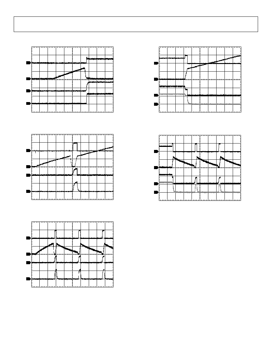
APPLICATIONS WAVEFORMS
05
64
7-
0
70
CH1 1.5A
CH2 1.00V
CH3 20.0V
CH4 10.0V
M40.0ms
4
3
2
1
Figure 41. Inrush Current Control into 220 F Load
(CH1 = I
LOAD
, CH2 = V
TIMER
, CH3 = V
GATE
, CH4 = V
OUT
)
05
64
7-
0
71
CH1 1.5A
CH2 1.00V
CH3 20.0V
CH4 10.0V
M10.0ms
4
3
2
1
Figure 42. Overcurrent Condition at Startup (ADM1175-1 Model)
(CH1 = I
LOAD
, CH2 = V
TIMER
, CH3 = V
GATE
, CH4 = V
OUT
)
05
64
7-
0
72
CH1 1.5A
CH2 1.00V
CH3 20.0V
CH4 10.0V
M20.0ms
4
3
2
1
Figure 43. Overcurrent Condition at Startup (ADM1175-2 Model)
(CH1 = I
LOAD
, CH2 = V
TIMER
, CH3 = V
GATE
, CH4 = V
OUT
)
05
64
7-
0
73
CH1 1.5A
CH2 1.00V
CH3 20.0V
CH4 10.0V
M10.0ms
4
3
2
1
Figure 44. Overcurrent Condition During Operation (ADM1175-1 Model)
(CH1 = I
LOAD
, CH2 = V
TIMER
, CH3 = V
GATE
, CH4 = V
OUT
)
05
64
7-
0
74
CH1 1.5A
CH2 1.00V
CH3 20.0V
CH4 10.0V
M20.0ms
4
3
2
1
Figure 45. Overcurrent Condition During Operation (ADM1175-2 Model)
(CH1 = I
LOAD
, CH2 = V
TIMER
, CH3 = V
GATE
, CH4 = V
OUT
)
ADM1175
Rev. 0 | Page 23 of 24
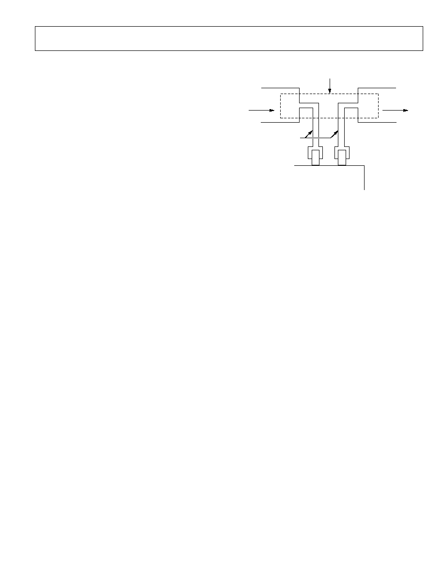
KELVIN SENSE RESISTOR CONNECTION
When using a low value sense resistor for high current
measurement, the problem of parasitic series resistance may
arise. The lead resistance can be a substantial fraction of the
rated resistance, making the total resistance a function of lead
length. This problem can be avoided by using a Kelvin sense
connection. This type of connection separates the current path
through the resistor and the voltage drop across the resistor.
Figure 46 shows the correct way to connect the sense resistor
between the VCC pin and the SENSE pin of the ADM1175.
SENSE RESISTOR
KELVIN SENSE TRACES
VCC
SENSE
ADM1175
CURRENT
FLOW FROM
SUPPLY
CURRENT
FLOW TO
LOAD
05
64
7-
01
5
Figure 46. Kelvin Sense Connections
ADM1175
Rev. 0 | Page 24 of 24
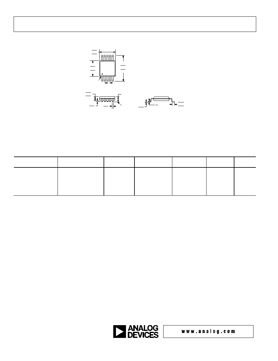
OUTLINE DIMENSIONS
COMPLIANT TO JEDEC STANDARDS MO-187-BA
0.23
0.08
0.80
0.60
0.40
8°
0°
0.15
0.05
0.33
0.17
0.95
0.85
0.75
SEATING
PLANE
1.10 MAX
10
6
5
1
0.50 BSC
PIN 1
COPLANARITY
0.10
3.10
3.00
2.90
3.10
3.00
2.90
5.15
4.90
4.65
Figure 47. 10-Lead Mini Small Outline Package [MSOP]
(RM-10)
Dimensions shown in millimeters
ORDERING GUIDE
Model
Hot Swap Retry Option
ON/ONB Pin
Temperature
Range
Package
Description
Package
Option Branding
ADM1175-1ARMZ-R7
1
Automatic Retry Version
ON
-40°C to +85°C
10-Lead MSOP
RM-10
M5P
ADM1175-2ARMZ-R7
1
Latched Off Version
ON
-40°C to +85°C
10-Lead MSOP
RM-10
M5R
ADM1175-3ARMZ-R7
1
Automatic Retry Version
ONB
-40°C to +85°C
10-Lead MSOP
RM-10
M5S
ADM1175-4ARMZ-R7
1
Latched Off Version
ONB
-40°C to +85°C
10-Lead MSOP
RM-10
M5T
EVAL-ADM1175EBZ
1
Evaluation
Board
1
Z = Pb-free part.
Purchase of licensed I
2
C components of Analog Devices or one of its sublicensed Associated Companies conveys a license for the purchaser under the Philips I
2
C Patent
Rights to use these components in an I
2
C system, provided that the system conforms to the I
2
C Standard Specification as defined by Philips.
©2006 Analog Devices, Inc. All rights reserved. Trademarks and
registered trademarks are the property of their respective owners.
D05647-0-9/06(0)
Document Outline
- þÿ
- þÿ
- þÿ
- þÿ
- þÿ
- þÿ
- þÿ
- þÿ
- þÿ
- þÿ
- þÿ
- þÿ
- þÿ
- þÿ