 | ÐлекÑÑоннÑй компоненÑ: ADG841 | СкаÑаÑÑ:  PDF PDF  ZIP ZIP |
ADG841/ADG842 0.28 ohm CMOS 1.65 V to 3.6 V Single SPST Switches in SC70 Data Sheet (Rev. 0)
0.28 CMOS 1.65 V to 3.6 V
Single SPST Switches in SC70
ADG841/ADG842
Rev. 0
Information furnished by Analog Devices is believed to be accurate and reliable.
However, no responsibility is assumed by Analog Devices for its use, nor any
infringements of patents or other rights of third parties that may result from its use.
Specifications subject to change without notice. No license is granted by implication
or otherwise under any patent or patent rights of Analog Devices. Trademarks and
registered trademarks are the property of their respective owners.
One Technology Way, P.O. Box 9106, Norwood, MA 02062-9106, U.S.A.
Tel: 781.329.4700
www.analog.com
Fax: 781.461.3113
© 2005 Analog Devices, Inc. All rights reserved.
FEATURES
Ultralow on resistance
0.28 typical
0.48 max at 125°C
Excellent audio performance, ultralow distortion
0.025 typical
0.052 max R
ON
flatness
1.65 V to 3.6 V single supply
High current carrying capability
300 mA continuous current
500 mA peak current
Automotive temperature range: 40°C to +125°C
Rail-to-rail operation
Typical power consumption (<0.01 µW)
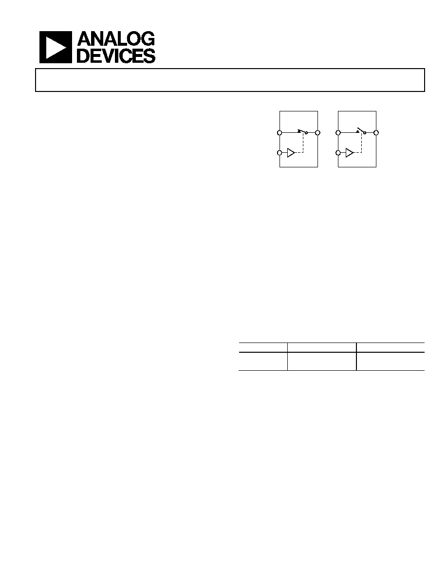
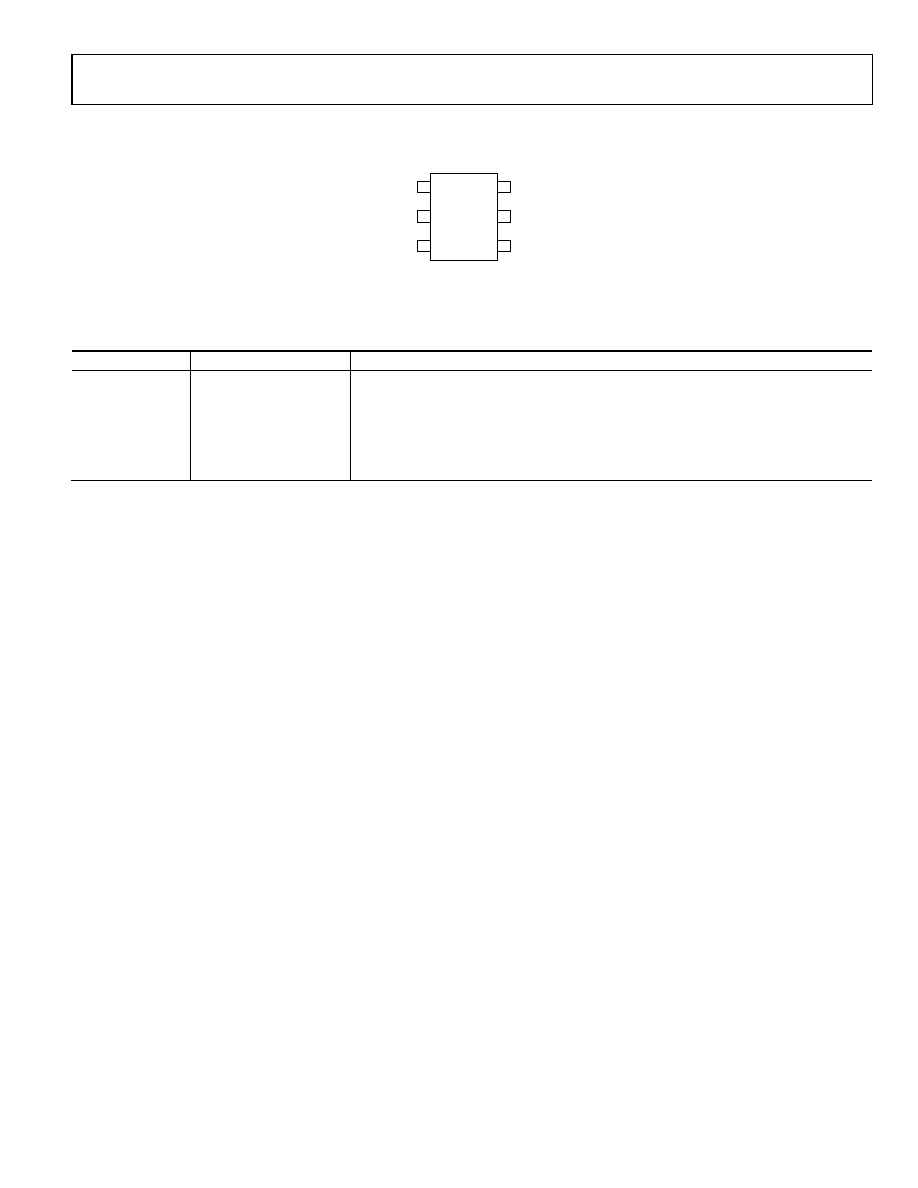
FUNCTIONAL BLOCK DIAGRAM
SWITCHES SHOWN
FOR A LOGIC 1 INPUT
ADG841
S
IN
D
05424-001
ADG842
S
IN
D
Figure 1.
APPLICATIONS
Handsets
PDAs
MP3 players
Power routing
Battery-powered systems
Communication systems
Modems
PCMCIA cards
GENERAL DESCRIPTION
The ADG841 and ADG842 are low voltage CMOS devices
containing a single-pole, single-throw (SPST) switch. The
ADG841 is closed for a Logic 1 input and the ADG842 is open
for a Logic 1 input. The devices offer ultralow on resistance of
less than 0.48 over the full temperature range. The ADG841/
ADG842 are fully specified for 3.3 V, 2.5 V, and 1.8 V supply
operation.
Each switch conducts equally well in both directions when on,
and has an input signal range that extends to the supplies. The
ADG841/ADG842 exhibit break-before-make switching action.
The ADG841/ADG842 are available in a 6-lead SC70 package.
PRODUCT HIGHLIGHTS
1.
<0.48 over full temperature range of 40°C to +125°C.
2.
Compatible with 1.8 V CMOS logic.
3.
High current handling capability (300 mA continuous
current at 3.3 V).
4.
Low THD + N (0.02% typ).
5.
Tiny SC70 package.
Table 1. ADG841/ADG842 Truth Table
Logic (IN)
ADG841
ADG842
0 Off
On
1 On
Off

ADG841/ADG842
Rev. 0 | Page 2 of 16
TABLE OF CONTENTS
Specifications--2.7 V to 3.6 V......................................................... 3
Specifications--2.5 V ± 0.2 V.......................................................... 4
Specifications--1.65 V to 1.95 ........................................................ 5
Absolute Maximum Ratings............................................................ 6
ESD Caution.................................................................................. 6
Pin Configuration and Function Descriptions............................. 7
Typical Performance Characteristics ..............................................8
Terminology .....................................................................................11
Test Circuits......................................................................................12
Outline Dimensions ........................................................................13
Ordering Guide ...........................................................................13
REVISION HISTORY
4/05--Revision 0: Initial Version
ADG841/ADG842
Rev. 0 | Page 3 of 16
SPECIFICATIONS--2.7 V TO 3.6 V
1
V
DD
= 2.7 V to 3.6 V, GND = 0 V, unless otherwise noted.
Table 2.
-40°C
-40°C
Parameter
+25°C
to +85°C
to +125°C Unit
Test
Conditions/Comments
ANALOG SWITCH
Analog Signal Range
0 V to V
DD
V
V
DD
= 2.7 V
On Resistance (R
ON
) 0.28
typ
V
DD
= 2.7 V, V
S
= 0 V to V
DD
, I
DS
= -100 mA
0.37
0.43
0.48
max
Figure 18
On Resistance Flatness (R
FLAT (ON)
) 0.025
typ V
DD
= 2.7 V, V
S
= 0 V to V
DD
, I
DS
= -100 mA
0.034
0.044
0.052
max
LEAKAGE CURRENTS
V
DD
= 3.6 V
Source Off Leakage I
S
(OFF)
±0.2
nA typ
V
S
= 0.6 V/3.3 V, V
D
= 3.3 V/0.6 V; Figure 19
Channel On Leakage I
D
, I
S
(ON)
±0.2
nA typ
V
S
= V
D
= 0.6 V or 3.3 V; Figure 20
DIGITAL INPUTS
Input High Voltage, V
INH
2
V
min
Input Low Voltage, V
INL
0.8
V
max
Input Current, I
INL
or I
INH
0.005
µA
typ
V
IN
= V
INL
or V
INH
±0.1
µA
max
Digital Input Capacitance, C
IN
3.2
pF
typ
DYNAMIC CHARACTERISTICS
2
t
ON
10.5
ns
typ
R
L
= 50 , C
L
= 35 pF
14
15.5
16.5
ns
max
V
S
= 1.5 V; Figure 21
t
OFF
6.5
ns
typ
R
L
= 50 , C
L
= 35 pF
7.8
8
8.2
ns
max
V
S
= 1.5 V; Figure 21
Charge Injection
200
pC typ
V
S
= 1.5 V, R
S
= 0 , C
L
= 1 nF; Figure 22
Off Isolation
-54
dB typ
R
L
= 50 , C
L
= 5 pF, f = 100 kHz; Figure 23
Total Harmonic Distortion (THD + N)
0.012
%
R
L
= 32 , f = 20 Hz to 20 kHz, V
S
= 3 V p-p
Insertion Loss
-0.02
dB typ
R
L
= 50 , C
L
= 5 pF; Figure 24
-3 dB Bandwidth
21
MHz typ
R
L
= 50 , C
L
= 5 pF; Figure 24
C
S
(OFF)
160
pF typ
C
D
(OFF)
160
pF typ
C
D
, C
S
(ON)
238
pF typ
POWER REQUIREMENTS
V
DD
= 3.6 V
I
DD
0.003
µA typ
Digital inputs = 0 V or 3.6 V
1
4
µA
max
1
Temperature range is -40°C to +125°C
2
Guaranteed by design; not subject to production test.

ADG841/ADG842
Rev. 0 | Page 4 of 16
SPECIFICATIONS--2.5 V ± 0.2 V
1
V
DD
= 2.5 V ± 0.2 V, GND = 0 V, unless otherwise noted.
Table 3.
-40°C
-40°C
Parameter
+25°C
to +85°C
to +125°C Unit
Test
Conditions/Comments
ANALOG SWITCH
Analog Signal Range
0 V to V
DD
V
On Resistance (R
ON
) 0.3
typ
V
DD
= 2.3 V, V
S
= 0 V to V
DD
, I
DS
= -100 mA
0.35
0.4
0.45
max
Figure 18
On Resistance Flatness (R
FLAT (ON)
) 0.025
typ
V
DD
= 2.3 V, V
S
= 0 V to V
DD
, I
DS
= -100 mA
0.04
0.05
0.05
max
LEAKAGE CURRENTS
V
DD
= 2.7 V
Source Off Leakage I
S
(OFF)
±0.2
nA typ
V
S
= 0.6 V/2.4 V, V
D
= 2.4 V/0.6 V; Figure 19
Channel On Leakage I
D
, I
S
(ON)
±0.2
nA typ
V
S
= V
D
= 0.6 V or 2.4 V; Figure 20
DIGITAL INPUTS
Input High Voltage, V
INH
1.7
V
min
Input Low Voltage, V
INL
0.7
V
max
Input Current, I
INL
or I
INH
0.005
µA
typ
V
IN
= V
INL
or V
INH
±0.1
µA
max
Digital Input Capacitance, C
IN
3.2
pF
typ
DYNAMIC CHARACTERISTICS
2
t
ON
13
ns
typ
R
L
= 50 , C
L
= 35 pF
16.5
18
19
ns
max
V
S
= 1.5 V; Figure 21
t
OFF
7
ns typ
R
L
= 50 , C
L
= 35 pF
8.2
8.4
8.6
ns
max
V
S
= 1.5 V; Figure 21
Charge Injection
150
pC typ
V
S
= 1.25 V, R
S
= 0 , C
L
= 1 nF; Figure 22
Off Isolation
-54
dB typ
R
L
= 50 , C
L
= 5 pF, f = 100 kHz; Figure 23
Total Harmonic Distortion (THD + N)
0.022
%
R
L
= 32 , f = 20 Hz to 20 kHz, V
S
= 1.5 V p-p
Insertion Loss
-0.02
dB typ
R
L
= 50 , C
L
= 5 pF; Figure 24
3 dB Bandwidth
21
MHz typ
R
L
= 50 , C
L
= 5 pF; Figure 24
C
S
(OFF) 170
pF
typ
C
D
(OFF) 170
pF
typ
C
D
, C
S
(ON)
238
pF typ
POWER REQUIREMENTS
V
DD
= 2.7 V
I
DD
0.003
µA typ
Digital inputs = 0 V or 2.7 V
1
4
µA
max
1
Temperature range is -40°C to +125°C.
2
Guaranteed by design; not subject to production test.
ADG841/ADG842
Rev. 0 | Page 5 of 16
SPECIFICATIONS--1.65 V TO 1.95
1
V
DD
= 1.65 V to1.95 V, GND = 0 V, unless otherwise noted.
Table 4.
-40°C
-40°C
Parameter
+25°C
to +85°C
to +125°C Unit
Test
Conditions/Comments
ANALOG SWITCH
Analog Signal Range
0 V to V
DD
V
On Resistance (R
ON
) 0.37
typ
V
DD
= 1.8 V, V
S
= 0 V to V
DD
, I
DS
= -100 mA
0.4
0.84
0.84
max
Figure 18
0.6
1.8
1.8
max
V
DD
= 1.65 V, V
S
= 0 V to V
DD
, I
DS
= -100 mA
On Resistance Flatness (R
FLAT (ON)
) 0.17
typ V
DD
= 1.65 V, V
S
= 0 V to V
DD
, I
DS
= -100 mA
LEAKAGE CURRENTS
V
DD
= 1.95 V
Source Off Leakage I
S
(OFF)
±0.2
nA typ
V
S
= 0.6 V/1.65 V, V
D
= 1.65 V/0.6 V; Figure 19
Channel On Leakage I
D
, I
S
(ON)
±0.2
nA typ
V
S
= V
D
= 0.6 V or 1.65 V; Figure 20
DIGITAL INPUTS
Input High Voltage, V
INH
0.65
V
DD
V
min
Input Low Voltage, V
INL
0.35
V
DD
V
max
Input Current, I
INL
or I
INH
0.005
µA
typ
V
IN
= V
INL
or V
INH
±0.1
µA
max
Digital Input Capacitance, C
IN
4
pF
typ
DYNAMIC CHARACTERISTICS
2
t
ON
19
ns
typ
R
L
= 50 , C
L
= 35 pF
26
28
30
ns
max
V
S
= 1.5 V; Figure 21
t
OFF
8
ns typ
R
L
= 50 , C
L
= 35 pF
9.5
9.8
10
ns
max
V
S
= 1.5 V; Figure 21
Charge Injection
100
pC typ
V
S
= 1 V, R
S
= 0 V, C
L
= 1 nF; Figure 22
Off Isolation
-54
dB typ
R
L
= 50 , C
L
= 5 pF, f = 100 kHz; Figure 23
Total Harmonic Distortion (THD + N)
0.14
%
R
L
= 32 , f = 20 Hz to 20 kHz, V
S
= 1.2 V p-p
Insertion Loss
-0.02
dB typ
R
L
= 50 , C
L
= 5 pF; Figure 24
3 dB Bandwidth
21
MHz typ
R
L
= 50 , C
L
= 5 pF; Figure 24
C
S
(OFF)
178
pF typ
C
D
(OFF)
178
pF typ
C
D
, C
S
(ON) 238
pF
typ
POWER REQUIREMENTS
V
DD
= 1.95 V
I
DD
0.003
µA typ
Digital inputs = 0 V or 1.95 V
1
4
µA
max
1
Temperature range -40°C to +125°C.
2
Guaranteed by design; not subject to production test.
ADG841/ADG842
Rev. 0 | Page 6 of 16
ABSOLUTE MAXIMUM RATINGS
T
A
= 25°C, unless otherwise noted.
Table 5.
Parameter Rating
V
DD
to GND
-0.3 V to +4.6 V
Analog Inputs
1
-0.3 V to V
DD
+ 0.3 V
Digital Inputs
1
-0.3 V to 4.6 V or 10 mA,
whichever occurs first
Peak Current, S or D
3.3 V Operation
500 mA
2.5 V Operation
460 mA
1.8 V Operation
420 mA (pulsed at 1 ms,
10% duty cycle max)
Continuous Current, S or D
3.3 V Operation
300 mA
2.5 V Operation
275 mA
1.8 V Operation
250 mA
Operating Temperature Range
Automotive (Y Version)
-40°C to +125°C
Storage Temperature Range
-65°C to +150°C
Junction Temperature
150°C
SC70 Package
JA
Thermal Impedance
494.8°C/W
Reflow Soldering (Pb-free)
Peak Temperature
260(+0/-5)°C
Time at Peak Temperature
10 sec to 40 sec
1
Overvoltages at S or D are clamped by internal diodes. Current should be
limited to the maximum ratings given.
Stresses above those listed under Absolute Maximum Ratings
may cause permanent damage to the device. This is a stress
rating only; functional operation of the device at these or any
other conditions above those indicated in the operational
section of this specification is not implied. Exposure to absolute
maximum rating conditions for extended periods may affect
device reliability. Only one absolute maximum rating may be
applied at any one time.
ESD CAUTION
ESD (electrostatic discharge) sensitive device. Electrostatic charges as high as 4000 V readily accumulate on
the human body and test equipment and can discharge without detection. Although this product features
proprietary ESD protection circuitry, permanent damage may occur on devices subjected to high energy
electrostatic discharges. Therefore, proper ESD precautions are recommended to avoid performance
degradation or loss of functionality.
ADG841/ADG842
Rev. 0 | Page 7 of 16
PIN CONFIGURATION AND FUNCTION DESCRIPTIONS
NC = NO CONNECT
D
1
S
2
GND
3
V
DD
6
NC
5
IN
4
ADG841/
ADG842
TOP VIEW
(Not to Scale)
05424-002
Figure 2. 6-Lead SC70
Table 6. Pin Function Descriptions
Pin No.
Mnemonic
Description
1
D
Drain Terminal. Can be an input or output.
2
S
Source Terminal. Can be an input or output.
3
GND
Ground (0 V) Reference.
4
IN
Logic Control Input.
5 NC
No
Connect.
6 V
DD
Most Positive Power Supply Potential.
ADG841/ADG842
Rev. 0 | Page 8 of 16
TYPICAL PERFORMANCE CHARACTERISTICS
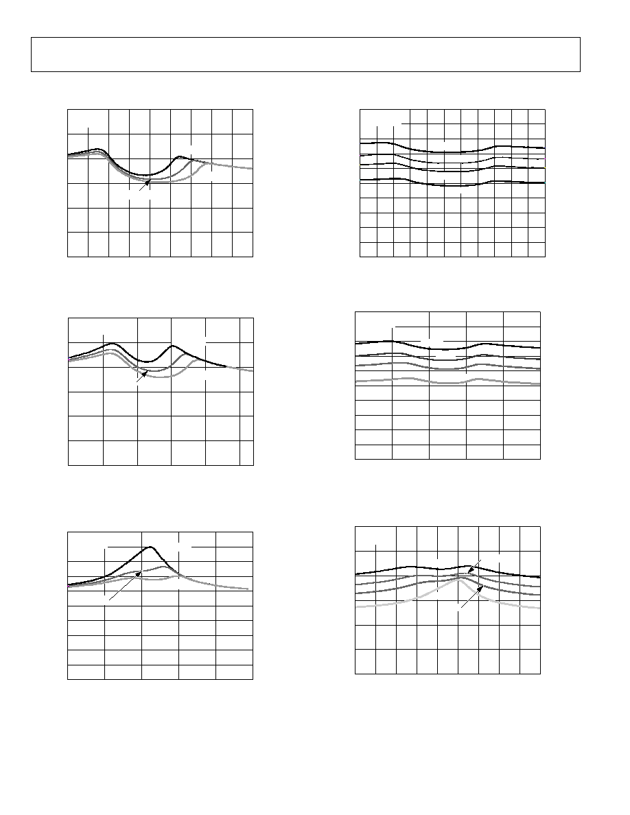
05424-003
SOURCE VOLTAGE (V)
3.6
0
0.4
0.8
1.2
1.6
2.0
2.4
2.8
3.2
ON RE
S
I
S
T
ANCE
(
)
0.350
0.325
0.300
0.275
0.250
0.225
0.200
V
DD
= 3.3V
V
DD
= 3.6V
V
DD
= 3V
T
A
= 25°C
I
DS
= 100mA
Figure 3. On Resistance vs. V
D
(V
S
) V
DD
= 3.3 V ± 0.3 V
05424-004
SOURCE VOLTAGE (V)
2.5
0
0.5
1.0
1.5
2.0
ON RE
S
I
S
T
ANCE
(
)
0.350
0.325
0.300
0.275
0.250
0.225
0.200
V
DD
= 2.3V
V
DD
= 2.7V
V
DD
= 2.5V
T
A
= 25°C
I
DS
= 100mA
Figure 4. On Resistance vs. V
D
(V
S
) V
DD
= 2.5 V ± 0.2 V
05424-005
SOURCE VOLTAGE (V)
2.0
0
0.4
0.8
1.2
1.6
ON RE
S
I
S
T
ANCE
(
)
0.50
0.40
0.45
0.30
0.35
0.20
0.25
0.10
0.05
0.15
0
V
DD
= 1.95V
V
DD
= 1.65V
T
A
= 25°C
I
DS
= 100mA
V
DD
= 1.8V
Figure 5. On Resistance vs. V
D
(V
S
) V
DD
= 1.8 V ± 0.15 V
05424-006
SOURCE VOLTAGE (V)
3.3
0
0.9
1.2
0.3
0.6
1.5
1.8
2.1
2.4
2.7
3.0
ON RE
S
I
S
T
ANCE
(
)
0.50
0.40
0.35
0.45
0.30
0.25
0.20
0.15
0.10
0.05
0
+85°C
+25°C
40°C
V
DD
= 3.3V
I
DS
= 100mA
+125°C
Figure 6. On Resistance vs. V
D
(V
S
) for Different Temperatures,V
DD
= 3.3 V
05424-007
SOURCE VOLTAGE (V)
2.5
0
0.5
1.0
1.5
2.0
ON RE
S
I
S
T
ANCE
(
)
0.50
0.45
0.40
0.35
0.30
0.25
0.20
0.15
0.10
0.05
0
40°C
+85°C
+25°C
+125°C
V
DD
= 2.5V
I
DS
= 100mA
Figure 7. On Resistance vs. V
D
(V
S
) for Different Temperatures, V
DD
= 2.5 V
05424-008
SOURCE VOLTAGE (V)
1.8
0
0.4
0.6
0.2
0.8
1.0
1.2
1.4
1.6
ON RE
S
I
S
T
ANCE
(
)
0.6
0.5
0.4
0.3
0.2
0.1
0
40°C
+85°C
V
DD
= 1.8V
I
DS
= 100mA
+25°C
+125°C
Figure 8. On Resistance vs. V
D
(V
S
) for Different Temperatures, V
DD
= 1.8 V
ADG841/ADG842
Rev. 0 | Page 9 of 16
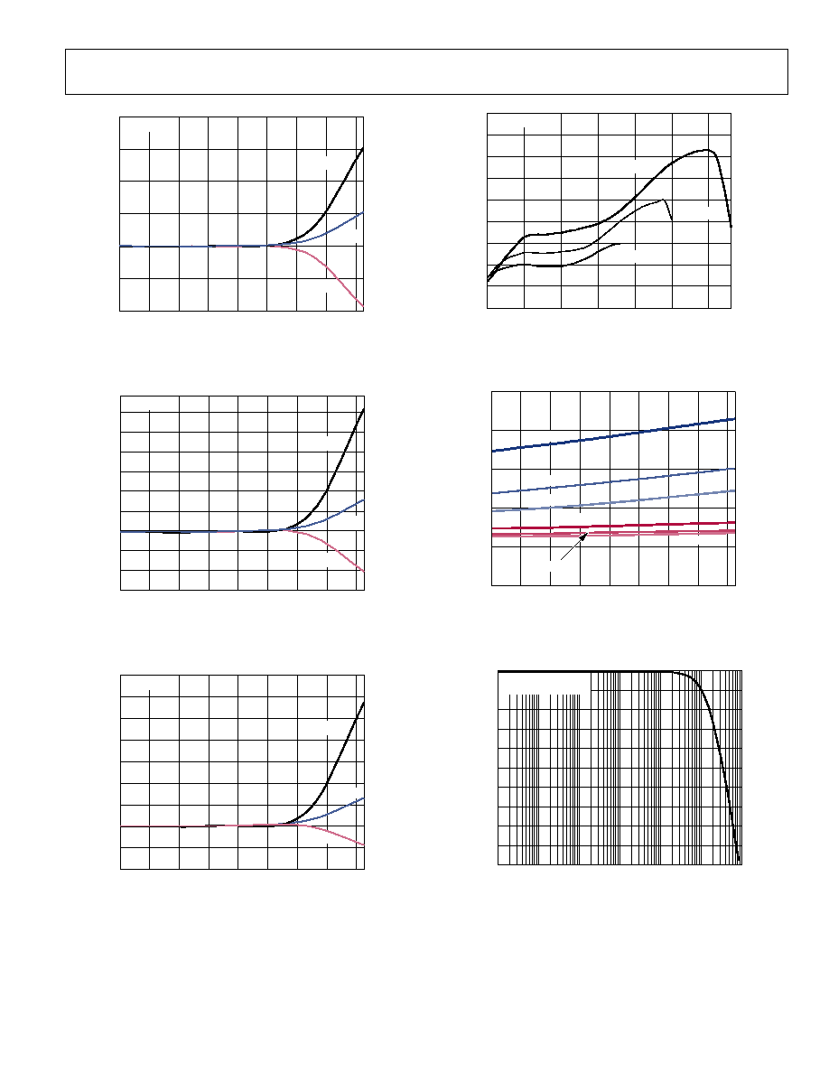
05424-009
TEMPERATURE (°C)
120
40
20
0
20
40
60
80
100
LE
AKAGE
(nA)
200
150
100
50
0
50
100
V
DD
= 3.3V
I
D
, I
S
(ON)
I
S
(OFF)
I
D
(OFF)
Figure 9. Leakage Current vs. Temperature, V
DD
= 3.3 V
05424-010
TEMPERATURE (°C)
120
40
0
20
20
40
60
80
100
LE
AKAGE
(nA)
140
100
120
40
20
80
60
0
20
40
60
V
DD
= 2.5V
I
D
, I
S
(ON)
I
S
(OFF)
I
D
(OFF)
Figure 10. Leakage Current vs. Temperature, V
DD
= 2.5 V
05424-011
TEMPERATURE
120
40
20
0
20
40
60
80
100
LE
AKAGE
(nA)
60
40
50
30
10
20
10
0
20
V
DD
= 1.8V
I
D
, I
S
(ON)
I
D
(OFF)
I
S
(OFF)
Figure 11. Leakage Current vs. Temperature, V
DD
= 1.8 V
05424-012
V
S
(V)
3.0
0
0.5
1.0
1.5
2.5
2.0
CHARGE
INJ
E
CTION (pC)
450
400
350
300
250
200
150
100
50
0
V
DD
= 3.3V
V
DD
= 2.5V
V
DD
= 1.8V
T
A
= 25°C
Figure 12. Charge Injection vs. Source Voltage
05424-013
TEMPERATURE (°C)
120
40
0
20
20
40
60
80
100
TIME (ns)
25
20
15
10
5
0
T
ON
T
OFF
V
DD
= 1.8V
V
DD
= 3.3V
V
DD
= 3.3V
V
DD
= 2.5V
V
DD
= 1.8V
V
DD
= 2.5V
Figure 13. t
ON
/t
OFF
Times vs. Temperature
05424-014
FREQUENCY (Hz)
100M
100
1k
10k
100k
1M
10M
ON
R
ESPON
SE (
d
B
)
0
1
2
3
4
5
6
7
8
9
10
T
A
= 25°C
V
DD
= 3.3V/2.5V/1.8V
Figure 14. Bandwidth
ADG841/ADG842
Rev. 0 | Page 10 of 16
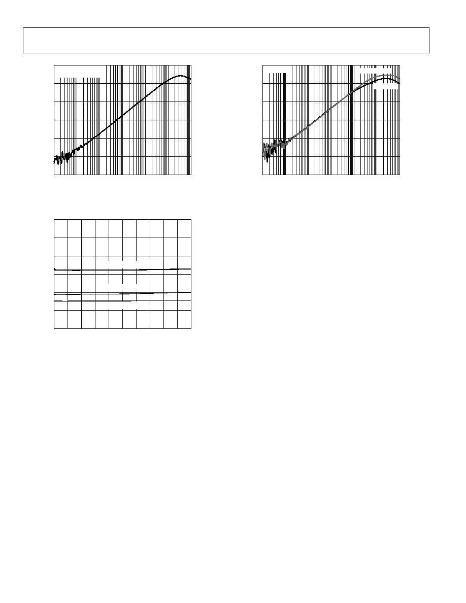
05424-015
FREQUENCY (Hz)
100M
100
1k
10k
100k
1M
10M
ON
R
ESPON
S
E
(
dB
)
0
20
40
80
60
100
120
T
A
= 25°C
V
DD
= 3.3V/2.5V/1.8V
Figure 15. Off Isolation vs. Frequency
05424-016
FREQUENCY (kHz)
20
0
2
4
6
8
10
12
14
16
18
THD + N (%)
0.030
0.025
0.020
0.015
0.010
0.005
0
V
DD
= 1.8V; V p-p = 1V
V
DD
= 2.5V; V p-p = 2V
V
DD
= 3.3V; V p-p = 2V
Figure 16. Total Harmonic Distortion + Noise
05424-017
FREQUENCY (Hz)
100M
100
1k
10k
100k
1M
10M
ON
R
ESPON
SE (
d
B
)
0
20
40
60
80
100
120
V
DD
= 1.8V
V
DD
= 3.3V / 2.5V
T
A
= 25°C
Figure 17. AC PSRR

ADG841/ADG842
Rev. 0 | Page 11 of 16
TERMINOLOGY
I
DD
Positive supply current.
V
D
(V
S
)
Analog voltage on Terminals D and S.
R
ON
Ohmic resistance between D and S.
R
FLAT (ON)
Flatness is the difference between the maximum and minimum
value of on resistance as measured over the specified analog
signal range.
I
S
(OFF)
Source leakage current with the switch off.
I
D
(OFF)
Drain leakage current with the switch off.
I
D
, I
S
(ON)
Channel leakage current with the switch on.
V
INL
Maximum input voltage for Logic 0.
V
INH
Minimum input voltage for Logic 1.
I
INL
(I
INH
)
Input current of the digital input.
C
S
(OFF)
Off switch source capacitance. Measured with reference to
ground.
C
D
(OFF)
Off switch drain capacitance. Measured with reference to
ground.
C
D
, C
S
(ON)
On switch capacitance. Measured with reference to ground.
C
IN
Digital input capacitance.
t
ON
Delay time between the 50% and the 90% points of the digital
input and switch on condition.
t
OFF
Delay time between the 50% and the 90% points of the digital
input and switch off condition.
Charge Injection
A measure of the glitch impulse transferred from the digital
input to the analog output during on-off switching.
Off Isolation
A measure of unwanted signal coupling through an off switch.
-3 dB Bandwidth
The frequency at which the output is attenuated by 3 dB.
On Response
The frequency response of the on switch.
Insertion Loss
The loss due to the on resistance of the switch.
THD + N
The ratio of the harmonics amplitude plus noise of a signal to
the fundamental.
PSRR
Power Supply Rejection Ratio. This is a measure of the coupling
of unwanted ac signals on the power supply to the switch output
when the supply is not decoupled.
ADG841/ADG842
Rev. 0 | Page 12 of 16
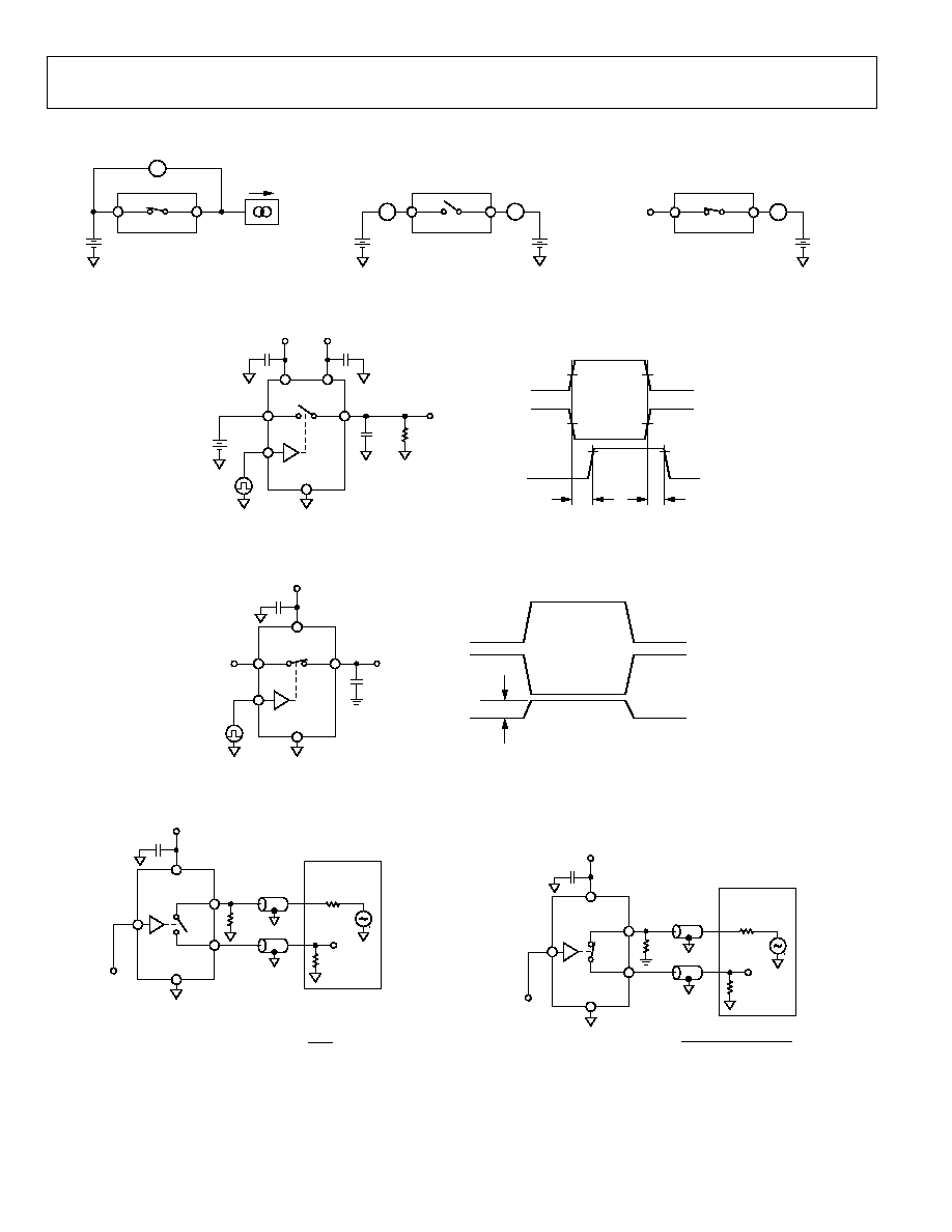
TEST CIRCUITS
S
D
V
S
V
I
DS
05424-017
Figure 18. On Resistance
I
S
(OFF)
I
D
(OFF)
05424-018
S
D
V
S
A
V
D
A
Figure 19. Off Leakage
05424-019
NC
I
D
(ON)
S
D
V
D
A
Figure 20. On Leakage
V
S
IN
S
D
GND
R
L
300
C
L
35pF
V
OUT
ADG841
ADG842
V
IN
V
IN
V
OUT
t
ON
t
OFF
50%
50%
90%
90%
50%
50%
V
DD
V
DD
V
SS
0.1
µ
F
V
SS
05424-020
0.1
µ
F
Figure 21. Switching Times, t
ON
, t
OFF
V
OUT
OFF
V
OUT
ON
Q
INJ
= C
L
×
V
OUT
V
IN
V
IN
ADG842
ADG841
05424-021
IN
D
S
GND
C
L
1nF
V
OUT
V
DD
V
S
V
DD
0.1
µ
F
Figure 22. Charge Injection
V
S
50
NETWORK
ANALYZER
R
L
50
OFF ISOLATION = 20 LOG
V
OUT
V
S
ADG841 V
IN
= 0
ADG842 V
IN
= 1
05424-022
IN
D
S
GND
50
V
DD
V
IN
V
OUT
V
DD
0.1
µ
F
Figure 23. Off Isolation
INSERTION LOSS = 20 LOG
V
OUT
WITH SWITCH
V
OUT
WITHOUT SWITCH
05424-023
V
S
50
NETWORK
ANALYZER
R
L
50
IN
D
S
GND
50
V
DD
V
IN
V
OUT
V
DD
0.1
µ
F
Figure 24. Bandwidth
ADG841/ADG842
Rev. 0 | Page 13 of 16
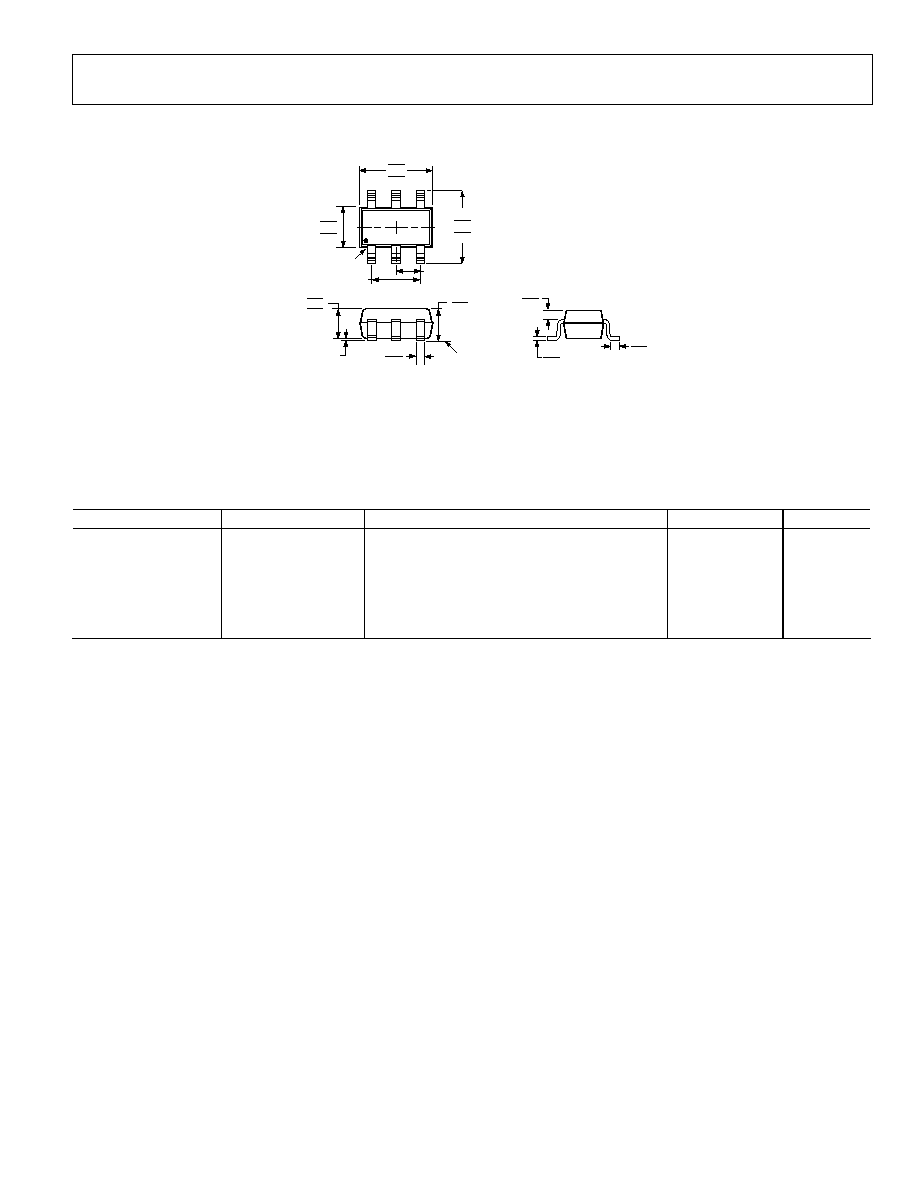
OUTLINE DIMENSIONS
COMPLIANT TO JEDEC STANDARDS MO-203-AB
0.22
0.08
0.30
0.10
0.30
0.15
1.00
0.90
0.70
SEATING
PLANE
4
5
6
3
2
1
PIN 1
0.65 BSC
1.30 BSC
0.10 MAX
0.10 COPLANARITY
0.40
0.10
1.10
0.80
2.20
2.00
1.80
2.40
2.10
1.80
1.35
1.25
1.15
Figure 25. 6-Lead Thin Shrink Small Outline Transistor [SC70]
(KS-6)
Dimensions shown in millimeters
ORDERING GUIDE
Model
Temperature Range
Package Description
Package Option
Branding
1
ADG841YKSZ-500RL7
2
40°C to +125°C
6-Lead Thin Shrink Small Outline Transistor (SC70)
KS-6
SVA
ADG841YKSZ-REEL
2
40°C to +125°C
6-Lead Thin Shrink Small Outline Transistor (SC70)
KS-6
SVA
ADG841YKSZ-REEL7
2
40°C to +125°C
6-Lead Thin Shrink Small Outline Transistor (SC70)
KS-6
SVA
ADG842YKSZ-500RL7
2
40°C to +125°C
6-Lead Thin Shrink Small Outline Transistor (SC70)
KS-6
SWA
ADG842YKSZ-REEL
2
40°C to +125°C
6-Lead Thin Shrink Small Outline Transistor (SC70)
KS-6
SWA
ADG842YKSZ-REEL
2
40°C to +125°C
6-Lead Thin Shrink Small Outline Transistor (SC70)
KS-6
SWA
1
Branding on this package is limited to three characters due to space constraints.
2
Z = Pb-free part.

ADG841/ADG842
Rev. 0 | Page 14 of 16
NOTES

ADG841/ADG842
Rev. 0 | Page 15 of 16
NOTES

ADG841/ADG842
Rev. 0 | Page 16 of 16
NOTES
© 2005 Analog Devices, Inc. All rights reserved. Trademarks and
registered trademarks are the property of their respective owners.
D05424-0-4/05(0)
Document Outline