 | ÐлекÑÑоннÑй компоненÑ: ADG836 | СкаÑаÑÑ:  PDF PDF  ZIP ZIP |
Äîêóìåíòàöèÿ è îïèñàíèÿ www.docs.chipfind.ru
Information furnished by Analog Devices is believed to be accurate and
reliable. However, no responsibility is assumed by Analog Devices for its
use, nor for any infringements of patents or other rights of third parties
that may result from its use. No license is granted by implication or oth-
erwise under any patent or patent rights of Analog Devices. Trademarks
and registered trademarks are the property of their respective companies.
One Technology Way, P.O. Box 9106, Norwood, MA 02062-9106, U.S.A.
Tel: 781/329-4700
www.analog.com
Fax: 781/326-8703 © 2003 Analog Devices, Inc. All rights reserved.
ADG836
0.5 CMOS 1.65 V TO 3.6 V
Dual SPDT/2:1 MUX
FEATURES
0.5 Typical On Resistance
0.8 Maximum On Resistance at 125°C
1.65 V to 3.6 V Operation
Automotive Temperature Range: 40°C to +125°C
High Current Carrying Capability: 300 mA Continuous
Rail-to-Rail Switching Operation
Fast Switching Times <20 ns
Typical Power Consumption (<0.1 W)
APPLICATIONS
Cellular Phones
PDAs
MP3 Players
Power Routing
Battery-Powered Systems
PCMCIA Cards
Modems
Audio and Video Signal Routing
Communication Systems
GENERAL DESCRIPTION
The ADG836 is a low voltage CMOS device containing two
independently selectable single-pole, double-throw (SPDT)
switches. This device offers ultralow on resistance of less than
0.8 over the full temperature range. The ADG836 is fully
specified for 3.3 V, 2.5 V, and 1.8 V supply operation.
Each switch conducts equally well in both directions when on
and has an input signal range that extends to the supplies. The
ADG836 exhibits break-before-make switching action.
The ADG836 is available in 10-lead MSOP and 3 mm 3 mm
12-lead LFCSP packages.
PRODUCT HIGHLIGHTS
1. <0.8 over full temperature range of 40°C to +125°C.
2. Single 1.65 V to 3.6 V operation.
3. Compatible with 1.8 V CMOS logic.
4. High current handling capability (300 mA continuous current
at 3.3 V).
5. Low THD + N (0.02% typ).
6. 3 mm 3 mm LFCSP package and 10-lead MSOP package.
FUNCTIONAL BLOCK DIAGRAM
REV. 0

2
ADG836SPECIFICATIONS
1
ADG836
3
40
C 40
C
Parameter
+25
C to +85
C to +125
C
Unit Test Conditions/Comments
ANALOG SWITCH
Analog Signal Range
0 V to V
DD
V V
DD
= 2.7 V
On Resistance (R
ON
)
0.5
typ V
DD
= 2.7 V, V
S
= 0 V to V
DD
, I
S
= 10 mA;
0.65 0.75 0.8
max Test Circuit 1
On Resistance Match between
0.04
typ V
DD
= 2.7 V, V
S
= 0.65 V, I
S
= 10 mA
Channels (R
ON
)
0.075 0.08
max
On Resistance Flatness (R
FLAT (ON)
)
0.1
typ V
DD
= 2.7 V, V
S
= 0 V to V
DD
,
0.15 0.16
max I
S
= 10 mA
LEAKAGE CURRENTS
V
DD
= 3.6 V
Source Off Leakage I
S
(OFF)
±0.2
nA typ V
S
= 0.6 V/3.3 V, V
D
= 3.3 V/0.6 V;
±1 ±10 ±100
nA max Test Circuit 2
Channel On Leakage I
D
, I
S
(ON)
±0.2
nA typ V
S
= V
D
= 0.6 V or 3.3 V; Test Circuit 3
±1 ±15 ±120
nA max
DIGITAL INPUTS
Input High Voltage, V
INH
2
V min
Input Low Voltage, V
INL
0.8
V max
Input Current
I
INL
or I
INH
0.005
µA typ V
IN
= V
INL
or V
INH
±0.1
µA max
C
IN
, Digital Input Capacitance
4
pF typ
DYNAMIC CHARACTERISTICS
2
t
ON
21
ns typ R
L
= 50
, C
L
= 35 pF
26 28 29
ns max V
S
= 1.5 V/0 V; Test Circuit 4
t
OFF
4
ns typ R
L
= 50
, C
L
= 35 pF
7 8 9
ns max V
S
= 1.5 V; Test Circuit 4
Break-before-Make Time Delay (t
BBM
)
17
ns typ R
L
= 50
, C
L
= 35 pF
5
ns min V
S1
= V
S2
= 1.5 V; Test Circuit 5
Charge Injection
40
pC typ V
S
= 1.5 V, R
S
= 0
, C
L
= 1 nF;
Test Circuit 6
Off Isolation
67
dB typ R
L
= 50
, C
L
= 5 pF, f = 100 kHz;
Test Circuit 7
Channel-to-Channel Crosstalk
90
dB typ S1AS2A/S1BS2B;
R
L
= 50
, C
L
= 5 pF, f = 100 kHz;
Test Circuit 10
67
dB typ S1AS1B/S2AS2B;
R
L
= 50
, C
L
= 5 pF, f = 100 kHz;
Test Circuit 9
Total Harmonic Distortion (THD + N) 0.02
% R
L
= 32
, f = 20 Hz to 20 kHz,
V
S
= 2 V p-p
Insertion Loss
0.05
dB typ R
L
= 50
, C
L
= 5 pF; Test Circuit 8
3 dB Bandwidth
57
MHz typ R
L
= 50
, C
L
= 5 pF; Test Circuit 8
C
S
(OFF)
25
pF typ
C
D
, C
S
(ON)
75
pF typ
POWER REQUIREMENTS
V
DD
= 3.6 V
I
DD
0.003
µA typ Digital Inputs = 0 V or 3.6 V
1 4
µA max
NOTES
1
Temperature range is as follows: Y version: 40°C to +125°C.
2
Guaranteed by design, not subject to production test.
Specifications subject to change without notice.
(V
DD
= 2.7 V to 3.6 V, GND = 0 V, unless otherwise noted.)
REV. 0
REV. 0

2
ADG836SPECIFICATIONS
1
ADG836
3
SPECIFICATIONS
1
40
C
40
C
Parameter +25
C to +85
C to +125
C
Unit Test Conditions/Comments
ANALOG SWITCH
Analog Signal Range
0 V to V
DD
V
On Resistance (R
ON
) 0.65
typ V
DD
= 2.3 V, V
S
= 0 V to V
DD
,
0.72 0.8
0.88
max I
S
= 10 mA; Test Circuit 1
On Resistance Match between 0.04
typ V
DD
= 2.3 V, V
S
= 0.7 V;
Channels (R
ON
) 0.08
0.085
max I
S
= 10 mA
On Resistance Flatness (R
FLAT (ON)
) 0.16
typ V
DD
= 2.3 V, V
S
= 0 V to V
DD
,
0.23
0.24
max I
S
= 10 mA
LEAKAGE CURRENTS
V
DD
= 2.7 V
Source Off Leakage I
S
(OFF) ±0.2
nA typ V
S
= 0.6 V/2.4 V, V
D
= 2.4 V/0.6 V;
±0.4 ±4
±45
nA max Test Circuit 2
Channel On Leakage I
D
, I
S
(ON) ±0.2
nA typ V
S
= V
D
= 0.6 V or 2.4 V; Test Circuit 3
±0.6 ±12
±90
nA max
DIGITAL INPUTS
Input High Voltage, V
INH
1.7
V min
Input Low Voltage, V
INL
0.7
V max
Input Current
I
INL
or I
INH
0.005
µA typ V
IN
= V
INL
or V
INH
±0.1
µA max
C
IN
, Digital Input Capacitance 4
pF typ
DYNAMIC CHARACTERISTICS
2
t
ON
23
ns typ R
L
= 50
, C
L
= 35 pF
29 30
31
ns max V
S
= 1.5 V/0 V; Test Circuit 4
t
OFF
5
ns typ R
L
= 50
, C
L
= 35 pF
7 8
9
ns max V
S
= 1.5 V; Test Circuit 4
Break-before-Make Time Delay (t
BBM
) 17
ns typ R
L
= 50
, C
L
= 35 pF
5
ns min V
S1
= V
S2
= 1.5 V; Test Circuit 5
Charge Injection 30
pC typ V
S
= 1.25 V, R
S
= 0
, C
L
= 1 nF;
Test Circuit 6
Off Isolation 67
dB typ R
L
= 50
, C
L
= 5 pF, f = 100 kHz;
Test Circuit 7
Channel-to-Channel Crosstalk 90
dB typ S1AS2A/S1BS2B;
R
L
= 50
, C
L
= 5 pF, f = 100 kHz;
Test Circuit 10
67
dB typ S1AS1B/S2AS2B;
R
L
= 50
, C
L
= 5 pF, f = 100 kHz;
Test Circuit 9
Total Harmonic Distortion (THD + N) 0.022
% R
L
= 32
, f = 20 Hz to 20 kHz,
V
S
= 1.5 V p-p
Insertion Loss 0.06
dB typ R
L
= 50
, C
L
= 5 pF; Test Circuit 8
3 dB Bandwidth 57
MHz typ R
L
= 50
, C
L
= 5 pF; Test Circuit 8
C
S
(OFF) 25
pF typ
C
D
, C
S
(ON) 75
pF typ
POWER REQUIREMENTS
V
DD
= 2.7 V
I
DD
0.003
µA typ Digital Inputs = 0 V or 2.7 V
1.0
4.0
µA max
NOTES
1
Temperature range is as follows: Y version: 40°C to +125°C.
2
Guaranteed by design, not subject to production test.
Specifications subject to change without notice.
(V
DD
= 2.5 V ± 0.2 V, GND = 0 V, unless otherwise noted.)
REV. 0
REV. 0

4
ADG836
ADG836
5
SPECIFICATIONS
1
40
C
40
C
Parameter +25
C to +85
C to +125
C
Unit Test Conditions/Comments
ANALOG SWITCH
Analog Signal Range
0 V to V
DD
V
On Resistance (R
ON
) 1
typ V
DD
= 1.8 V, V
S
= 0 V to V
DD
, I
S
= 10 mA;
1.4
2.2
2.2
max Test Circuit 1
2
4
4
max V
DD
= 1.65 V, V
S
= 0 V to V
DD
, I
S
= 10 mA
On Resistance Match between 0.1
typ V
DD
= 1.65 V, V
S
= 0.7 V, I
S
= 10 mA
Channels (R
ON
)
LEAKAGE CURRENTS
V
DD
= 1.95 V
Source Off Leakage I
S
(OFF) ±0.2
nA typ V
S
= 0.6 V/1.65 V, V
D
= 1.65 V/0.6 V;
±0.4
±4
±25
nA max Test Circuit 2
Channel On Leakage I
D
, I
S
(ON) ±0.2
nA typ V
S
= V
D
= 0.6 V or 1.65 V; Test Circuit 3
±0.6
±10
±75
nA max
DIGITAL INPUTS
Input High Voltage, V
INH
0.65 V
DD
V min
Input Low Voltage, V
INL
0.35 V
DD
V max
Input Current
I
INL
or I
INH
0.005
µA typ V
IN
= V
INL
or V
INH
±0.1
µA max
C
IN
, Digital Input Capacitance 4
pF typ
DYNAMIC CHARACTERISTICS
2
t
ON
28
ns typ R
L
= 50
, C
L
= 35 pF
37
38
39
ns max V
S
= 1.5 V/0 V; Test Circuit 4
t
OFF
7
ns typ R
L
= 50
, C
L
= 35 pF
9
10
11
ns max V
S
= 1.5 V/0 V; Test Circuit 4
Break-before-Make Time Delay (t
BBM
) 21
ns typ R
L
= 50
, C
L
= 35 pF
5
ns min V
S1
= V
S2
= 1 V; Test Circuit 5
Charge Injection 20
pC typ V
S
= 1 V, R
S
= 0
, C
L
= 1 nF;
Test Circuit 6
Off Isolation 67
dB typ R
L
= 50
, C
L
= 5 pF, f = 100 kHz;
Test Circuit 7
Channel-to-Channel Crosstalk 90
dB typ S1AS2A/S1BS2B;
R
L
= 50
, C
L
= 5 pF, f = 100 kHz;
Test Circuit 10
67
dB typ S1AS1B/S2AS2B;
R
L
= 50
, C
L
= 5 pF, f = 100 kHz;
Test Circuit 9
Total Harmonic Distortion, THD 0.14
% R
L
= 32
, f = 20 Hz to 20 kHz,
V
S
= 1.2 V p-p
Insertion Loss 0.08
dB typ R
L
= 50
, C
L
= 5 pF; Test Circuit 8
3 dB Bandwidth 57
MHz typ R
L
= 50
, C
L
= 5 pF; Test Circuit 8
C
S
(OFF) 25
pF typ
C
D
, C
S
(ON) 75
pF typ
POWER REQUIREMENTS
V
DD
= 1.95 V
I
DD
0.003
µA typ Digital Inputs = 0 V or 1.95 V
1.0
4
µA max
NOTES
1
Temperature range is as follows: Y version: 40°C to +125°C.
2
Guaranteed by design, not subject to production test.
Specifications subject to change without notice.
(V
DD
= 1.65 V to 1.95 V, GND = 0 V, unless otherwise noted.)
REV. 0
REV. 0
4
ADG836
ADG836
5
ABSOLUTE MAXIMUM RATINGS
1
(T
A
= 25°C, unless otherwise noted.)
V
DD
to GND . . . . . . . . . . . . . . . . . . . . . . . . . . 0.3 V to +4.6 V
Analog Inputs
2
. . . . . . . . . . . . . . . . . . . . . 0.3 V to V
DD
+ 0.3 V
Digital Inputs
2
. . . . . . . . . . . . . . . . . . . . . . . . . . 0.3 V to 4.6 V
or 10 mA, Whichever Occurs First
Peak Current, S or D
3.3 V Operation . . . . . . . . . . . . . . . . . . . . . . . . . . . . . 500 mA
2.5 V Operation . . . . . . . . . . . . . . . . . . . . . . . . . . . . . 460 mA
1.8 V Operation . . . . . . . . . . . . . . . . . . . . . . . . . . . . . 420 mA
(Pulsed at 1ms, 10% Duty Cycle Max)
Continuous Current, S or D
3.3 V Operation
300 mA
2.5 V Operation
275 mA
1.8 V Operation
250 mA
Operating Temperature Range
Automotive (Y Version) . . . . . . . . . . . . . . . . 40°C to +125°C
Storage Temperature Range . . . . . . . . . . . . . . 65°C to +150°C
Junction Temperature . . . . . . . . . . . . . . . . . . . . . . . . . . . .150°C
MSOP Package
JA
Thermal Impedance . . . . . . . . . . . . . . . . . . . . . . 206°C/W
JC
Thermal Impedance . . . . . . . . . . . . . . . . . . . . . . . 44°C/W
LFCSP Package
JA
Thermal Impedance (3-Layer Board) . . . . . . . . . 61.1°C/W
IR Reflow, Peak Temperature <20 sec . . . . . . . . . . . . . . . .235°C
NOTES
1
Stresses above those listed under Absolute Maximum Ratings may cause permanent
damage to the device. This is a stress rating only; functional operation of the device
at these or any other conditions above those listed in the operational sections of this
specification is not implied. Exposure to absolute maximum rating conditions for
extended periods may affect device reliability. Only one absolute maximum rating
may be applied at any one time.
2
Overvoltages at IN, S, or D will be clamped by internal diodes. Current should be
limited to the maximum ratings given.
CAUTION
ESD (electrostatic discharge) sensitive device. Electrostatic charges as high as 4000 V readily accumulate
on the human body and test equipment and can discharge without detection. Although the ADG836
features proprietary ESD protection circuitry, permanent damage may occur on devices subjected to high
energy electrostatic discharges. Therefore, proper ESD precautions are recommended to avoid performance
degradation or loss of functionality.
Table I. ADG836 Truth Table
Logic Switch A Switch B
0 Off On
1 On Off
ORDERING GUIDE
Model Temperature Range Package Description Package Option Branding*
ADG836YRM 40°C to +125°C Mini Small Outline Package (MSOP) RM-10 S9A
ADG836YRM-REEL 40°C to +125°C Mini Small Outline Package (MSOP) RM-10 S9A
ADG836YRM-REEL7 40°C to +125°C Mini Small Outline Package (MSOP) RM-10 S9A
ADG836YCP 40°C to +125°C Lead Frame Chip Scale Package (LFCSP) CP-12 S9A
ADG836YCP-REEL 40°C to +125°C Lead Frame Chip Scale Package (LFCSP) CP-12 S9A
ADG836YCP-REEL7 40°C to +125°C Lead Frame Chip Scale Package (LFCSP) CP-12 S9A
*Branding on this package is limited to three characters due to space constraints.
REV. 0
REV. 0
ADG836
6
7
Typical Performance CharacteristicsADG836
TERMINOLOGY
V
DD
Most positive power supply potential.
I
DD
Positive supply current.
GND Ground (0 V) reference.
S Source terminal. May be an input or output.
D Drain terminal. May be an input or output.
IN Logic control input.
V
D
(V
S
) Analog voltage on terminals D, S.
R
ON
Ohmic resistance between D and S.
R
FLAT (ON)
Flatness is defined as the difference between the maximum and minimum value of on resistance as measured
over the specified analog signal range.
R
ON
On resistance match between any two channels.
I
S
(OFF) Source leakage current with the switch off.
I
D
(OFF) Drain leakage current with the switch off.
I
D
, I
S
(ON) Channel leakage current with the switch on.
V
INL
Maximum input voltage for Logic 0.
V
INH
Minimum input voltage for Logic 1.
I
INL
(I
INH
) Input current of the digital input.
C
S
(OFF) Off switch source capacitance. Measured with reference to ground.
C
D
(OFF) Off switch drain capacitance. Measured with reference to ground.
C
D
, C
S
(ON) On switch capacitance. Measured with reference to ground.
C
IN
Digital input capacitance.
t
ON
Delay time between the 50% and the 90% points of the digital input and switch on condition.
t
OFF
Delay time between the 50% and the 90% points of the digital input and switch off condition.
t
BBM
On or off time measured between the 80% points of both switches when switching from one to another.
Charge Injection A measure of the glitch impulse transferred from the digital input to the analog output during on-off switching.
Off Isolation A measure of unwanted signal coupling through an off switch.
Crosstalk A measure of unwanted signal which is coupled through from one channel to another as a result of parasitic
capacitance.
3 dB Bandwidth The frequency at which the output is attenuated by 3 dB.
On Response The frequency response of the on switch.
Insertion Loss The loss due to the on resistance of the switch.
THD + N The ratio of the harmonics amplitude plus noise of a signal, to the fundamental.
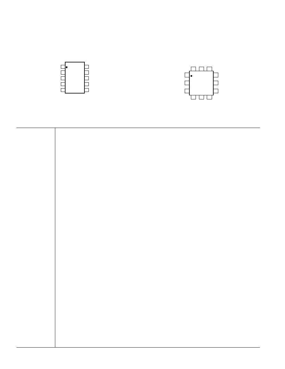
10-Lead MSOP
(RM-10)
12-Lead LFCSP
(CP-12)
PIN CONFIGURATIONS
REV. 0
REV. 0
ADG836
6
7
Typical Performance CharacteristicsADG836
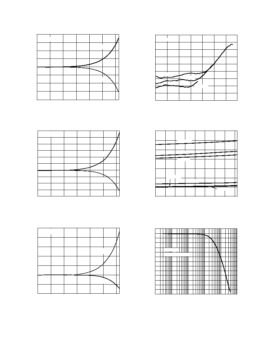
0.60
0.55
0.50
0.45
ON RESIST
ANCE
(
)
0.40
0.35
0.30
0.25
0.20
0
0.5
1.0
1.5
2.0
2.5
3.0
3.5
V
D
, V
S
(V)
V
DD
= 2.7V
V
DD
= 3V
T
A
= 25C
V
DD
= 3.6V
V
DD
= 3.3V
TPC 1. On Resistance vs. V
D
(V
S
) V
DD
= 2.7 V to 3.6 V
0.8
ON RESIST
ANCE
(
)
0.3
0.4
0.5
0.6
0.7
0.2
0
0.5
2.5
2.0
1.5
1.0
V
D
, V
S
(V)
T
A
= 25C
V
DD
= 2.5V
V
DD
= 2.3V
V
DD
= 2.7V
TPC 2. On Resistance vs. V
D
(V
S
) V
DD
= 2.5 V ± 0.2 V
1.8
ON RESIST
ANCE
(
)
0.4
0.6
0.8
1.0
1.2
1.4
1.6
0.2
0
0.2
0.4
0.6
0.8
1.0
1.2
1.4
1.6
1.8
2.0
V
D
, V
S
(V)
T
A
= 25C
V
DD
= 1.65V
V
DD
= 1.8V
V
DD
= 1.95V
TPC 3. On Resistance vs. V
D
(V
S
), V
DD
= 1.8 V ± 0.15 V
1.2
ON RESIST
ANCE
(
)
0.2
0.4
0.6
0.8
1.0
0
0
3.0
2.5
2.0
1.5
1.0
0.5
V
D
, V
S
(V)
+125C
+85C
+25C
40C
V
DD
= 3.3V
TPC 4. On Resistance vs. V
D
(V
S
) for Different
Temperatures, 3.3 V
1.2
ON RESIST
ANCE
(
)
0.2
0.4
0.6
0.8
1.0
0
0
2.5
2.0
1.5
1.0
0.5
V
D
, V
S
(V)
+125C
+25C
V
DD
= 2.5V
+85C
40C
TPC 5. On Resistance vs. V
D
(V
S
) for Different
Temperature, 2.5 V
1.4
ON RESIST
ANCE
(
)
0.2
0.5
0.7
0.8
1.0
1.2
0
0
1.8
0.2
0.4
0.6
0.8
1.0
1.2
1.4
1.6
V
D
, V
S
(V)
+25C
40C
+85C
+125C
V
DD
= 1.8V
TPC 6. On Resistance vs. V
D
(V
S
) for
Different Temperatures, 1.8 V
REV. 0
REV. 0
ADG836
8
ADG836
9
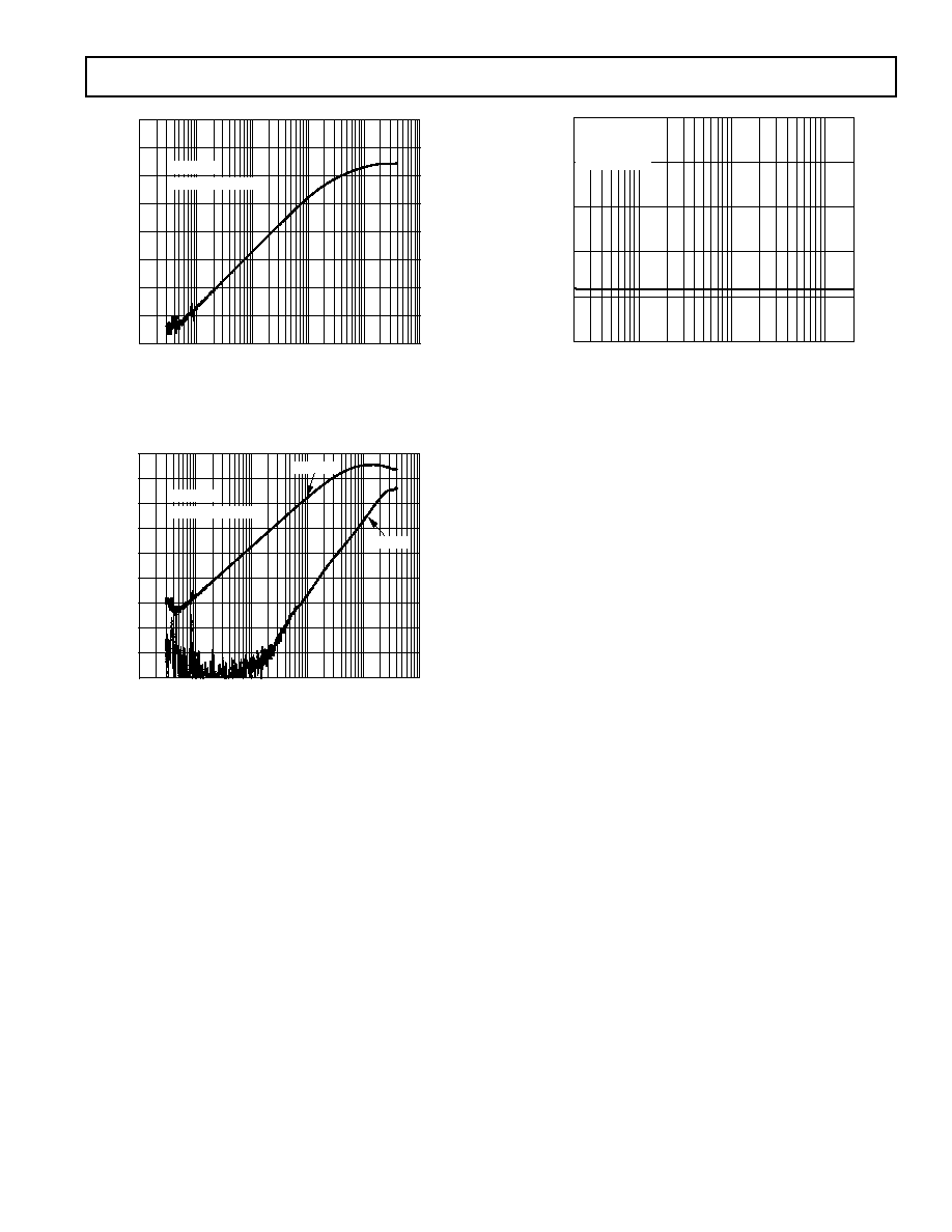
0
20
80
60
20
40
60
80
40
0
20
60
40
80
100
120
I
D
, I
S
(ON)
I
S
(OFF)
V
DD
= 3.3V
TPC 7. Leakage Currents vs. Temperature, 3.3 V
60
CURRENT (nA)
30
20
10
0
10
20
30
40
50
40
0
120
100
80
60
40
20
TEMPERATURE (C)
V
DD
= 2.5V
I
D
, I
S
(ON)
I
S
(OFF)
TPC 8. Leakage Current vs. Temperature, 2.5 V
50
CURRENT (nA)
20
10
10
0
20
30
40
0
120
100
80
60
40
20
TEMPERATURE (C)
V
DD
= 1.8V
I
S
, I
D
(ON)
I
S
(OFF)
TPC 9. Leakage Current vs. Temperature, 1.8 V
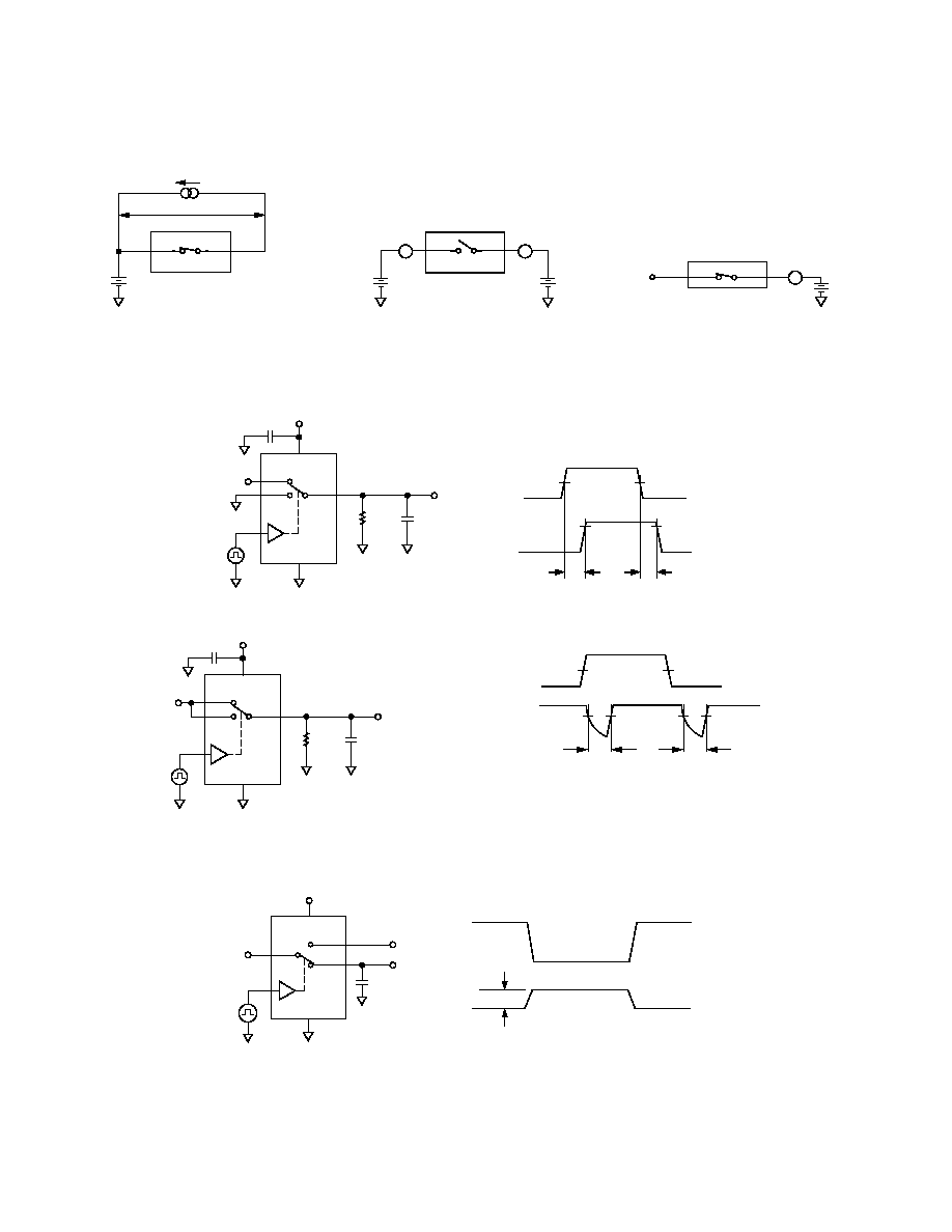
0
10
20
30
40
50
60
70
80
90
0
0.5
1.0
1.5
2.0
2.5
3.0
3.5
T
A
= 25ºC
V
CC
= 3.3V
V
CC
= 2.5V
V
CC
= 1.8V
TPC 10. Charge Injection vs. Source Voltage
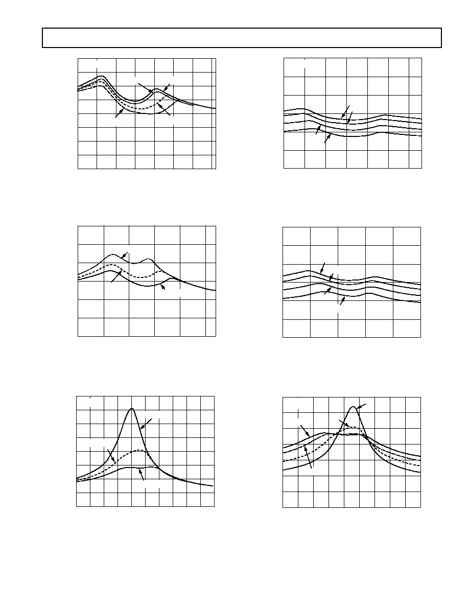
TPC 11.
t
ON
/
t
OFF
Times vs. Temperature
A
T
T
E
N
U
A
T
I
O
N
(
d
B
)
V
CC
= 3.3V/2.5V/1.8V
T
A
= 25ºC
TPC 12. Bandwidth
REV. 0
REV. 0
ADG836
8
ADG836
9
80
70
60
50
40
30
20
10
0
A
T
T
E
N
U
A
T
I
O
N
(
d
B
)
V
CC
= 3.3V/2.5V/1.8V
T
A
= 25ºC
TPC 13. Off Isolation vs. Frequency
100
90
80
70
60
50
40
30
20
10
A
T
T
E
N
U
A
T
I
O
N
(
d
B
)
V
CC
= 3.3V/2.5V/1.8V
T
A
= 25ºC
TPC 14. Crosstalk vs. Frequency
0.10
THD + N (%
)
0
0.02
0.04
0.06
0.08
20
20k
100
50
200
1k
500
2k
10k
5k
FREQUENCY (Hz)
V
DD
= 2.5V
T
A
= 25C
S1AD1
32 LOAD
1.5V p-p
TPC 15. Total Harmonic Distortion + Noise
REV. 0
REV. 0
10
ADG836
ADG836
11
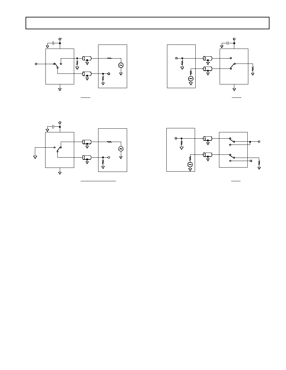
Test Circuit 4. Switching Times,
t
ON
,
t
OFF
Test Circuit 5. Break-before-Make Time Delay,
t
BBM
Test Circuit 6. Charge Injection
Test Circuits
Test Circuit 1. On Resistance
Test Circuit 2. Off Leakage
Test Circuit 3. On Leakage
REV. 0
REV. 0
10
ADG836
ADG836
11
Test Circuit 7. Off Isolation
Test Circuit 8. Bandwidth
Test Circuit 9. Channel-to-Channel Crosstalk (S1AS1B)
Test Circuit 10. Channel-to-Channel Crosstalk (S1AS2A)
REV. 0
REV. 0
C0430808/03(0)
12
ADG836
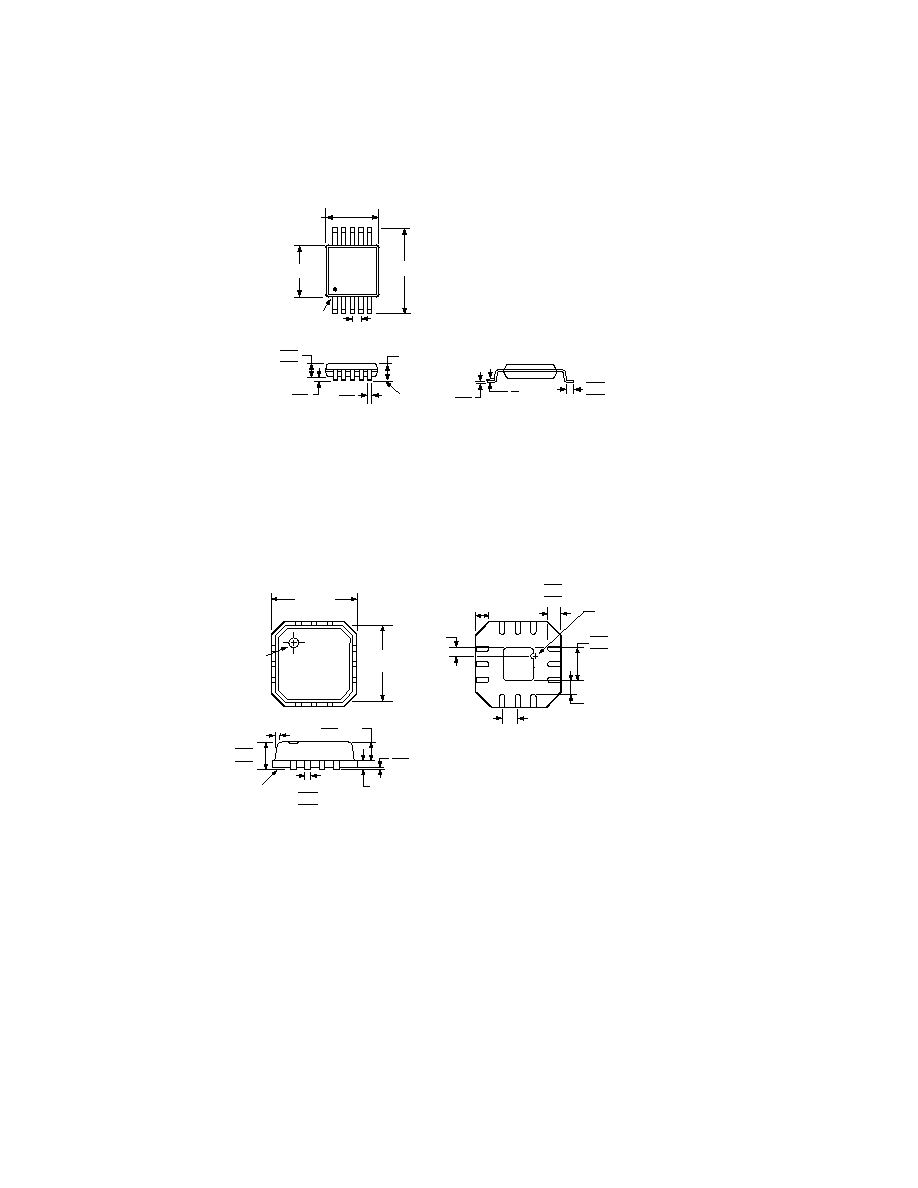
OUTLINE DIMENSIONS
10-Lead Mini Small Outline Package [MSOP]
(RM-10)
Dimensions shown in millimeters
0.23
0.08
0.80
0.60
0.40
8
0
0.15
0.00
0.27
0.17
0.95
0.85
0.75
SEATING
PLANE
1.10 MAX
10
6
5
1
0.50 BSC
3.00 BSC
3.00 BSC
4.90 BSC
PIN 1
COPLANARITY
0.10
COMPLIANT TO JEDEC STANDARDS MO-187BA
12-Lead Lead Frame Chip Scale Package [LFCSP]
(CP-12)
Dimensions shown in millimeters
1
0.50
BSC
0.60 MAX
PIN 1 INDICATOR
0.75
0.55
0.35
0.25 MIN
0.45
TOP
VIEW
12 MAX
0.80 MAX
0.65 TYP
SEATING
PLANE
PIN 1
INDICATOR
1.00
0.85
0.80
0.30
0.23
0.18
0.05 MAX
0.02 NOM
0.20 REF
1.45
1.30
1.15
BOTTOM
VIEW
12
4
10
6
7
9
3
2.75
BSC SQ
3.00
BSC SQ
2
5
8
11
SQ*
COPLANARITY
0.08
*COMPLIANT TO JEDEC STANDARDS MO-220-VEED-1
EXCEPT FOR EXPOSED PAD DIMENSION
REV. 0
Document Outline
- FEATURES
- APPLICATIONS
- FUNCTIONAL BLOCK DIAGRAM
- GENERAL DESCRIPTION
- PRODUCT HIGHLIGHTS
- SPECIFICATIONS
- ABSOLUTE MAXIMUM RATINGS
- ORDERING GUIDE
- PIN CONFIGURATIONS
- TERMINOLOGY
- Typical Performance Characteristics
- Test Circuits
- OUTLINE DIMENSIONS