 | ÐлекÑÑоннÑй компоненÑ: ADG1207 | СкаÑаÑÑ:  PDF PDF  ZIP ZIP |
ADG1206/ADG1207 Low Capacitance, 16- and 8-Channel ±15 V/+12 V iCMOS Multiplexers Data Sheet (Rev. 0)
Low Capacitance, 16- and 8-Channel
±15 V/+12 V iCMOS
TM
Multiplexers
ADG1206/ADG1207
Rev. 0
Information furnished by Analog Devices is believed to be accurate and reliable. However, no
responsibility is assumed by Analog Devices for its use, nor for any infringements of patents or other
rights of third parties that may result from its use. Specifications subject to change without notice. No
license is granted by implication or otherwise under any patent or patent rights of Analog Devices.
Trademarks and registered trademarks are the property of their respective owners.
One Technology Way, P.O. Box 9106, Norwood, MA 02062-9106, U.S.A.
Tel: 781.329.4700
www.analog.com
Fax: 781.461.3113
©2006 Analog Devices, Inc. All rights reserved.
FEATURES
<1 pC charge injection over full signal range
1.5 pF off capacitance
33 V supply range
120 on resistance
Fully specified at ±15 V/+12 V
3 V logic-compatible inputs
Rail-to-rail operation
Break-before-make switching action
28-lead TSSOP and 32-lead, 5 mm × 5 mm LFCSP_VQ
APPLICATIONS
Audio and video routing
Automatic test equipment
Data acquisition systems
Battery-powered systems
Sample-and-hold systems
Communication systems
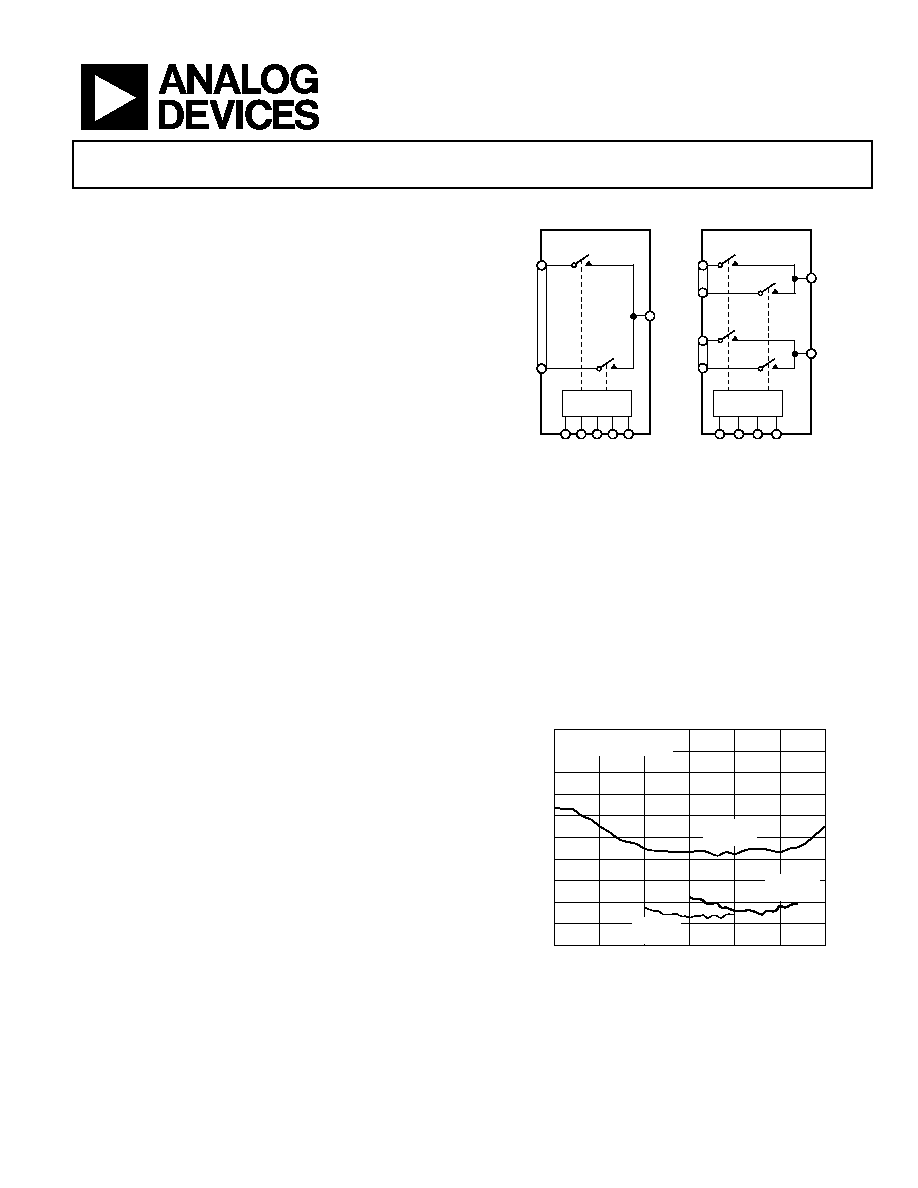
FUNCTIONAL BLOCK DIAGRAMS
ADG1207
S1A
S8B
DA
DB
S8A
S1B
1-OF-8
DECODER
A0 A1 A2 EN
ADG1206
S1
S16
D
1-OF-16
DECODER
A0 A1 A2 A3 EN
06
11
9-
0
01
Figure 1.
GENERAL DESCRIPTION
The ADG1206 and ADG1207 are monolithic iCMOS analog
multiplexers comprising sixteen single channels and eight
differential channels, respectively. The ADG1206 switches one
of sixteen inputs to a common output, as determined by the 4-
bit binary address lines A0, A1, A2, and A3. The ADG1207
switches one of eight differential inputs to a common
differential output, as determined by the 3-bit binary address
lines A0, A1, and A2. An EN input on both devices is used to
enable or disable the device. When disabled, all channels are
switched off. When on, each channel conducts equally well in
both directions and has an input signal range that extends to the
supplies.
The iCMOS (industrial CMOS) modular manufacturing
process combines high voltage CMOS (complementary metal-
oxide semiconductor) and bipolar technologies. It enables the
development of a wide range of high performance analog ICs
capable of 33 V operation in a footprint that no other generation
of high voltage parts has been able to achieve. Unlike analog ICs
using conventional CMOS processes, iCMOS components can
tolerate high supply voltages while providing increased perfor-
mance, dramatically lower power consumption, and reduced
package size.
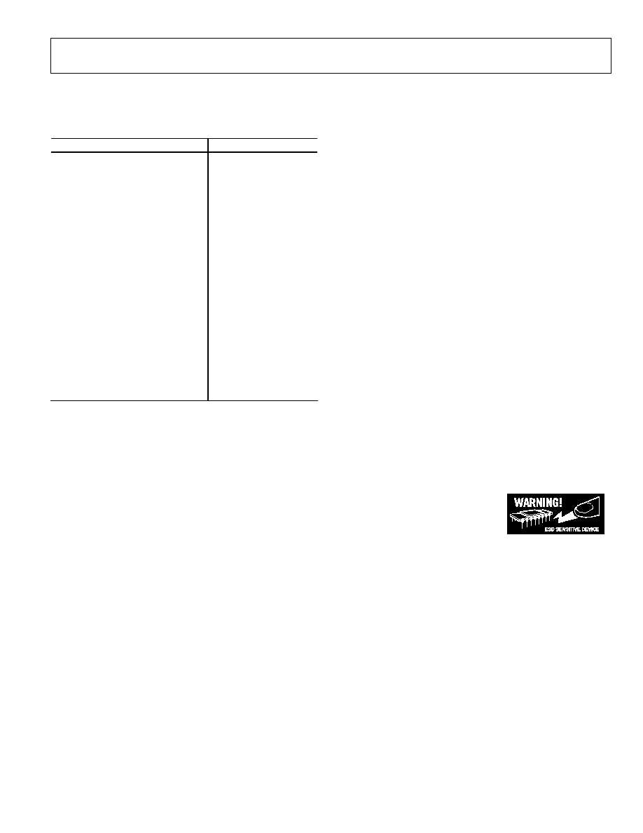
The ultralow capacitance and exceptionally low charge injection
of these multiplexers make them ideal solutions for data
acquisition and sample-and-hold applications, where low glitch
and fast settling are required. Figure 2 shows that there is
minimum charge injection over the entire signal range of the
device. iCMOS construction also ensures ultralow power
dissipation, making the parts ideally suited for portable and
battery-powered instruments.
V
S
(V)
CH
ARG
E
I
N
JE
CT
I
O
N
(
p
C)
1.0
0
15
15
0.9
0.8
0.7
0.6
0.5
0.4
0.3
0.2
0.1
10
5
0
5
10
MUX (SOURCE TO DRAIN)
T
A
= 25°C
V
DD
= +15V
V
SS
= 15V
V
DD
= +5V
V
SS
= 5V
V
DD
= +12V
V
SS
= 0V
0
61
19
-
0
02
Figure 2. Source-to-Drain Charge Injection vs. Source Voltage

ADG1206/ADG1207
Rev. 0 | Page 2 of 20
TABLE OF CONTENTS
Features .............................................................................................. 1
Applications....................................................................................... 1
Functional Block Diagrams............................................................. 1
General Description ......................................................................... 1
Revision History ............................................................................... 2
Specifications..................................................................................... 3
Dual Supply ................................................................................... 3
Single Supply ................................................................................. 5
Absolute Maximum Ratings ............................................................7
ESD Caution...................................................................................7
Pin Configurations and Function Descriptions ............................8
Typical Performance Characteristics ........................................... 12
Terminology .................................................................................... 16
Test Circuits..................................................................................... 17
Outline Dimensions ....................................................................... 19
Ordering Guide .......................................................................... 19
REVISION HISTORY
7/06--Revision 0: Initial Version

ADG1206/ADG1207
Rev. 0 | Page 3 of 20
SPECIFICATIONS
DUAL SUPPLY
V
DD
= +15 V ± 10%, V
SS
= 15 V ± 10%, GND = 0 V, unless otherwise noted.
1
Table 1.
Parameter +25°C
-40°C to
+85°C
-40°C to
+125°C
Unit
Test Conditions/Comments
ANALOG SWITCH
Analog Signal Range
V
SS
to V
DD
V
On Resistance, R
ON
120
typ
V
S
= ±10 V, I
S
= -1 mA; see Figure 28
200
240
270
max
V
DD
= +13.5 V, V
SS
= -13.5 V
On Resistance Match Between
Channels, R
ON
3.5
typ
V
S
= ±10 V, I
S
= -1 mA
6
10
12
max
On Resistance Flatness, R
FLAT
(On)
20
typ
V
S
= -5 V, 0 V, +5 V; I
S
= -1 mA
64
76
83
max
LEAKAGE CURRENTS
Source Off Leakage, I
S
(Off )
±0.03
nA typ
V
D
= ±10 V, V
S
=
10 V; see Figure 29
±0.2
±0.6
±1
nA max
Drain Off Leakage, I
D
(Off )
±0.05
nA typ
V
S
= 1 V, 10 V; V
D
= 10 V, 1 V; see Figure 29
±0.2
±0.6
±2
nA
max
Channel On Leakage, I
D
, I
S
(On)
±0.08
nA typ
V
S
= V
D
= ±10 V; see Figure 30
±0.2
±0.6
±2
nA
max
DIGITAL
INPUTS
Input High Voltage, V
INH
2.0
V
min
Input Low Voltage, V
INL
0.8
V
max
Input Current, I
INL
or I
INH
±0.005
A
typ
V
IN
= V
INL
or V
INH
±0.1
A
max
Digital Input Capacitance, C
IN
2
pF
typ
DYNAMIC CHARACTERISTICS
2
Transition Time, t
TRANSITION
80
ns typ
R
L
= 300 , C
L
= 35 pF
130
165
185
ns max
V
S
= 10 V; see Figure 31
t
ON
(EN)
75
ns typ
R
L
= 300 , C
L
= 35 pF
95
105
115
ns max
V
S
= 10 V; see Figure 33
t
OFF
(EN)
85
ns typ
R
L
= 300 , C
L
= 35 pF
100
125
140
ns max
V
S
= 10 V; see Figure 33
Break-Before-Make Time Delay, t
BBM
20
ns typ
R
L
= 300 , C
L
= 35 pF
10
ns min
V
S1
= V
S2
= 10 V; see Figure 32
Charge Injection
0.5
pC typ
V
S
= 0 V, R
S
= 0 , C
L
= 1 nF; see Figure 34
Off Isolation
-85
dB typ
R
L
= 50 , C
L
= 5 pF, f = 1 MHz; see Figure 35
Channel-to-Channel Crosstalk
-85
dB typ
R
L
= 50 , C
L
= 5 pF, f = 1 MHz; see Figure 37
Total Harmonic Distortion + Noise
0.15
% typ
R
L
= 10 k, 5 V rms, f = 20 Hz to 20 kHz;
see Figure 38
-3 dB Bandwidth ADG1206
280
MHz typ
R
L
= 50 , C
L
= 5 pF; see Figure 36
-3 dB Bandwidth ADG1207
490
MHz typ
R
L
= 50 , C
L
= 5 pF; see Figure 36
C
S
(Off )
1.5
pF typ
f = 1 MHz, V
S
= 0 V
2
pF max
f = 1 MHz, V
S
= 0 V
C
D
(Off ) ADG1206
11
pF typ
f = 1 MHz, V
S
= 0 V
12
pF max
f = 1 MHz, V
S
= 0 V
C
D
(Off ) ADG1207
7
pF typ
f = 1 MHz, V
S
= 0 V
9
pF max
f = 1 MHz, V
S
= 0 V

ADG1206/ADG1207
Rev. 0 | Page 4 of 20
Parameter +25°C
-40°C to
+85°C
-40°C to
+125°C
Unit
Test Conditions/Comments
C
D
, C
S
(On) ADG1206
13
pF typ
f = 1 MHz, V
S
= 0 V
15
pF max
f = 1 MHz, V
S
= 0 V
C
D
, C
S
(On) ADG1207
8
pF typ
f = 1 MHz, V
S
= 0 V
10
pF max
f = 1 MHz, V
S
= 0 V
POWER REQUIREMENTS
V
DD
= +16.5 V, V
SS
= -16.5 V
I
DD
0.002
A typ
Digital inputs = 0 V or V
DD
1.0
A max
I
DD
260
A typ
Digital inputs = 5 V
420
A
max
I
SS
0.002
A typ
Digital inputs = 0 V, 5 V, or V
DD
1.0
A max
V
DD
/V
SS
±5/±16.5
V min/max
GND = 0V
1
Temperature range for Y version is
-40°C to +125°C.
2
Guaranteed by design, not subject to production test.

ADG1206/ADG1207
Rev. 0 | Page 5 of 20
SINGLE SUPPLY
V
DD
= 12 V ± 10%, V
SS
= 0 V, GND = 0 V, unless otherwise noted.
1
Table 2.
Parameter +25°C
-40°C to
+85°C
-40°C to
+125°C Unit
Test
Conditions/Comments
ANALOG SWITCH
Analog Signal Range
0 to V
DD
V
On Resistance, R
ON
300
typ
V
S
= 0 V to10 V, I
S
= -1 mA; see Figure 28
475
567
625
max
V
DD
= 10.8 V, V
SS
= 0 V
On Resistance Match Between
Channels, R
ON
5
typ V
S
= 0 V to 10 V, I
S
= -1 mA
16
26
27
max
On Resistance Flatness, R
FLAT
(On)
60
typ
V
S
= 3 V, 6 V, 9 V; I
S
= -1 mA
LEAKAGE CURRENTS
V
DD
= 13.2 V
Source Off Leakage, I
S
(Off )
±0.02
nA typ
V
S
= 1 V/10 V, V
D
= 10 V/1 V; see Figure 29
±0.2
±0.6
±1
nA max
Drain Off Leakage, I
D
(Off )
±0.05
nA typ
V
S
= 1 V/10 V, V
D
= 10 V/1 V; see Figure 29
±0.2
±0.6
±2
nA
max
Channel On Leakage, I
D
, I
S
(On)
±0.08
nA typ
V
S
= V
D
= 1 V or 10 V; see Figure 30
±0.2
±0.6
±2
nA max
DIGITAL INPUTS
Input High Voltage, V
INH
2.0
V
min
Input Low Voltage, V
INL
0.8
V
max
Input Current, I
INL
or I
INH
±0.001
A
typ
±0.1
A
max
V
IN
= V
INL
or V
INH
Digital Input Capacitance, C
IN
3
pF
typ
DYNAMIC CHARACTERISTICS
2
Transition Time, t
TRANSITION
100
ns
typ
R
L
= 300 , C
L
= 35 pF
140
175
200
ns
max
V
S
= 8 V; see Figure 31
t
ON
(EN)
80
ns typ
R
L
= 300 , C
L
= 35 pF
100
120
130
ns
max
V
S
= 8 V; see Figure 33
t
OFF
(EN)
90
ns typ
R
L
= 300 , C
L
= 35 pF
110
130
155
ns
max
V
S
= 8 V; see Figure 33
Break-Before-Make Time Delay, t
BBM
25
ns
typ R
L
= 300 , C
L
= 35 pF
15
ns
min
V
S1
= V
S2
= 8 V; see Figure 32
Charge Injection
0.2
pC typ
V
S
= 6 V, R
S
= 0 , C
L
= 1 nF; see Figure 34
Off Isolation
-85
dB typ
R
L
= 50 , C
L
= 5 pF, f = 1 MHz; see Figure 35
Channel-to-Channel Crosstalk
-85
dB typ
R
L
= 50 , C
L
= 5 pF, f = 1 MHz; see Figure 37
-3 dB Bandwidth ADG1206
185
MHz typ
R
L
= 50 , C
L
= 5 pF; see Figure 36
-3 dB Bandwidth ADG1207
300
MHz typ
R
L
= 50 , C
L
= 5 pF; see Figure 36
C
S
(Off )
1.5
pF typ
f = 1 MHz, V
S
= 6 V
2
pF max
f = 1 MHz, V
S
= 6 V
C
D
(Off ) ADG1206
13
pF typ
f = 1 MHz, V
S
= 6 V
15
pF max
f = 1 MHz, V
S
= 6 V
C
D
(Off ) ADG1207
9
pF typ
f = 1 MHz, V
S
= 6 V
11
pF max
f = 1 MHz, V
S
= 6 V
C
D
, C
S
(On) ADG1206
15
pF typ
f = 1 MHz, V
S
= 6 V
17
pF max
f = 1 MHz, V
S
= 6 V
C
D
, C
S
(On) ADG1207
10
pF typ
f = 1 MHz, V
S
= 6 V
12
pF max
f = 1 MHz, V
S
= 6 V

ADG1206/ADG1207
Rev. 0 | Page 6 of 20
Parameter +25°C
-40°C to
+85°C
-40°C to
+125°C Unit
Test
Conditions/Comments
POWER REQUIREMENTS
V
DD
= 13.2 V
I
DD
0.002
A typ
Digital inputs = 0 V or V
DD
1.0
A max
I
DD
260
A typ
Digital inputs = 5
420
A
max
V
DD
5/16.5
V
min/max
V
SS
= 0 V, GND = 0 V
1
Temperature range for Y version is -40°C to +125°C.
2
Guaranteed by design, not subject to production test.
ADG1206/ADG1207
Rev. 0 | Page 7 of 20
ABSOLUTE MAXIMUM RATINGS
T
A
= 25°C, unless otherwise noted.
Table 3.
Parameter Rating
V
DD
to V
SS
35
V
V
DD
to GND
-0.3 V to +25 V
V
SS
to GND
+0.3 V to -25 V
Analog, Digital Inputs
1
V
SS
- 0.3 V to V
DD
+ 0.3 V
or 30 mA, whichever
occurs first
Continuous Current, S or D
30 mA
Peak Current, S or D (Pulsed at 1 ms,
10% Duty Cycle Maximum)
100 mA
Operating Temperature Ranges
Industrial (Y Version)
40°C to +125°C
Storage
65°C to +150°C
Junction Temperature
150°C
28-Lead TSSOP
JA
, Thermal Impedance
97.9°C/W
JC
, Thermal Impedance
14°C/W
32-Lead LFCSP_VQ
JA
, Thermal Impedance
27.27°C/W
Reflow Soldering Peak Temperature
(Pb-Free)
260(+0/-5)°C
1
Overvoltages at A, EN, S, or D are clamped by internal diodes. Current should
be limited to the maximum ratings given.
Stresses above those listed under Absolute Maximum Ratings
may cause permanent damage to the device. This is a stress
rating only; functional operation of the device at these or any
other conditions above those indicated in the operational
section of this specification is not implied. Exposure to absolute
maximum rating conditions for extended periods may affect
device reliability.
Only one absolute maximum rating may be applied at any
one time.
ESD CAUTION
ESD (electrostatic discharge) sensitive device. Electrostatic charges as high as 4000 V readily accumulate on
the human body and test equipment and can discharge without detection. Although this product features
proprietary ESD protection circuitry, permanent damage may occur on devices subjected to high energy
electrostatic discharges. Therefore, proper ESD precautions are recommended to avoid performance
degradation or loss of functionality.
ADG1206/ADG1207
Rev. 0 | Page 8 of 20
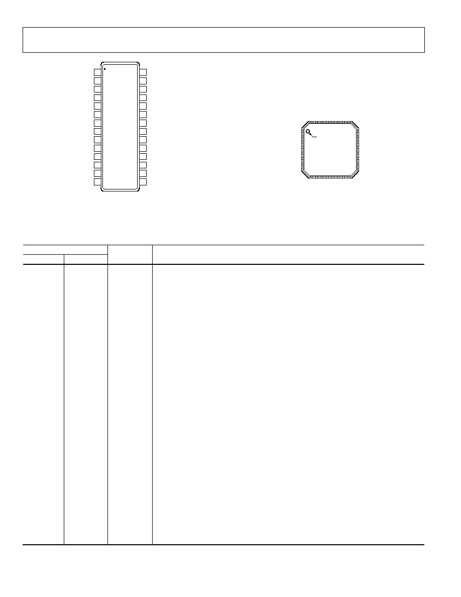
PIN CONFIGURATIONS AND FUNCTION DESCRIPTIONS
1
V
DD
28
D
2
NC
27
V
SS
3
NC
26
S8
4
S16
25
S7
5
S15
24
S6
6
S14
23
S5
7
S13
22
S4
8
S12
21
S3
9
S11
20
S2
10
S10
19
S1
11
S9
18
EN
12
GND
17
A0
13
NC
16
A1
14
A3
15
A2
ADG1206
TOP VIEW
(Not to Scale)
NC = NO CONNECT
06
11
9-
00
3
NC = NO CONNECT
PIN 1
INDICATOR
1
S16
2
S15
3
S14
4
S13
5
S12
6
S11
7
S10
8
S9
24 S8
23 S7
22 S6
21 S5
20 S4
19 S3
18 S2
17 S1
9
G
N
D
1
0
A
3
1
1
A
2
1
2
N
C
1
3
N
C
1
4
A
1
1
5
A
0
1
6
E
N
3
2
N
C
3
1
V
D
D
3
0
D
2
9
N
C
2
8
N
C
2
7
N
C
2
6
N
C
2
5
V
S
S
TOP VIEW
(Not to Scale)
ADG1206
06
11
9-
0
04
Figure 3. ADG1206 Pin Configuration--TSSOP
Figure 4. ADG1206 Pin Configuration--5 mm × 5 mm LFCSP_VQ,
Exposed Pad Tied to Substrate, V
SS
Table 4. ADG1206 Pin Function Descriptions
Pin Number
TSSOP LFCSP_VQ
Mnemonic
Description
1 31 V
DD
Most Positive Power Supply Potential.
2
12, 13
NC
No Connect.
3
26, 27, 28,
30, 32
NC No
Connect.
4
1
S16
Source Terminal 16. Can be an input or an output.
5
2
S15
Source Terminal 15. Can be an input or an output.
6
3
S14
Source Terminal 14. Can be an input or an output.
7
4
S13
Source Terminal 13. Can be an input or an output.
8
5
S12
Source Terminal 12. Can be an input or an output.
9
6
S11
Source Terminal 11. Can be an input or an output.
10
7
S10
Source Terminal 10. Can be an input or an output.
11
8
S9
Source Terminal 9. Can be an input or an output.
12
9
GND
Ground (0 V) Reference.
13
NC No
Connect.
14
10
A3
Logic Control Input.
15
11
A2
Logic Control Input.
16
14
A1
Logic Control Input.
17
15
A0
Logic Control Input.
18 16 EN Active High Digital Input. When this pin is low, the device is disabled and all switches are
turned off. When this pin is high, the Ax logic inputs determine which switch is turned on.
19
17
S1
Source Terminal 1. Can be an input or an output.
20
18
S2
Source Terminal 2. Can be an input or an output.
21
19
S3
Source Terminal 3. Can be an input or an output.
22
20
S4
Source Terminal 4. Can be an input or an output.
23
21
S5
Source Terminal 5. Can be an input or an output.
24
22
S6
Source Terminal 6. Can be an input or an output.
25
23
S7
Source Terminal 7. Can be an input or an output.
26
24
S8
Source Terminal 8. Can be an input or an output.
27 25 V
SS
Most Negative Power Supply Potential. In single-supply applications, this pin can be
connected to ground.
28
29
D
Drain Terminal. Can be an input or an output.
ADG1206/ADG1207
Rev. 0 | Page 9 of 20
Table 5. ADG1206 Truth Table
A3
A2
A1
A0
EN
On Switch
X
X
X
X
0
None
0
0
0
0
1
1
0
0
0
1
1
2
0
0
1
0
1
3
0
0
1
1
1
4
0
1
0
0
1
5
0
1
0
1
1
6
0
1
1
0
1
7
0
1
1
1
1
8
1
0
0
0
1
9
1
0
0
1
1
10
1
0
1
0
1
11
1
0
1
1
1
12
1
1
0
0
1
13
1
1
0
1
1
14
1
1
1
0
1
15
1
1
1
1
1
16
ADG1206/ADG1207
Rev. 0 | Page 10 of 20
1
V
DD
28
DA
2
DB
27
V
SS
3
NC
26
S8A
4
S8B
25
S7A
5
S7B
24
S6A
6
S6B
23
S5A
7
S5B
22
S4A
8
S4B
21
S3A
9
S3B
20
S2A
10
S2B
19
S1A
11
S1B
18
EN
12
GND
17
A0
13
NC
16
A1
14
NC
15
A2
ADG1207
TOP VIEW
(Not to Scale)
NC = NO CONNECT
06
11
9-
03
6
NC = NO CONNECT
PIN 1
INDICATOR
1
S8B
2
S7B
3
S6B
4
S5B
5
S4B
6
S3B
7
S2B
8
S1B
24 S8A
23 S7A
22 S6A
21 S5A
20 S4A
19 S3A
18 S2A
17 S1A
9
G
N
D
1
0
A
2
1
1
N
C
1
2
N
C
1
3
N
C
1
4
A
1
1
5
A
0
1
6
E
N
3
2
N
C
3
1
D
B
3
0
V
D
D
2
9
N
C
2
8
N
C
2
7
D
A
2
6
N
C
2
5
V
S
S
TOP VIEW
(Not to Scale)
ADG1207
06
11
9-
0
37
Figure 5. ADG1207 Pin Configuration--TSSOP
Figure 6. ADG1207 Pin Configuration--5 mm × 5 mm LFCSP_VQ
Exposed Pad Tied to Substrate, V
SS
Table 6. ADG1207 Pin Function Descriptions
Pin Number
TSSOP LFCSP_VQ
Mnemonic
Description
1 29 V
DD
Most Positive Power Supply Potential.
2
31
DB
Drain Terminal B. Can be an input or an output.
3 11,
12,
13
NC No
Connect.
4
1
S8B
Source Terminal 8B. Can be an input or an output.
5
2
S7B
Source Terminal 7B. Can be an input or an output.
6
3
S6B
Source Terminal 6B. Can be an input or an output.
7
4
S5B
Source Terminal 5B. Can be an input or an output.
8
5
S4B
Source Terminal 4B. Can be an input or an output.
9
6
S3B
Source Terminal 3B. Can be an input or an output.
10
7
S2B
Source Terminal 2B. Can be an input or an output.
11
8
S1B
Source Terminal 1B. Can be an input or an output.
12
9
GND
Ground (0 V) Reference.
13
26, 28,
30, 32
NC No
Connect.
14
NC No
Connect.
15
10
A2
Logic Control Input.
16
14
A1
Logic Control Input.
17
15
A0
Logic Control Input.
18 16 EN Active High Digital Input. When this pin is low, the device is disabled and all switches are
turned off. When this pin is high, the Ax logic inputs determine which switch is turned on.
19
17
S1A
Source Terminal 1A. Can be an input or an output.
20
18
S2A
Source Terminal 2A. Can be an input or an output.
21
19
S3A
Source Terminal 3A. Can be an input or an output.
22
20
S4A
Source Terminal 4A. Can be an input or an output.
23
21
S5A
Source Terminal 5A. Can be an input or an output.
24
22
S6A
Source Terminal 6A. Can be an input or an output.
25
23
S7A
Source Terminal 7A. Can be an input or an output.
26
24
S8A
Source Terminal 8A. Can be an input or an output.
27 25 V
SS
Most Negative Power Supply Potential. In single-supply applications, this pin can be
connected to ground.
28
27
DA
Drain Terminal A. Can be an input or an output.

ADG1206/ADG1207
Rev. 0 | Page 11 of 20
Table 7. ADG1207 Truth Table
A2
A1
A0
EN
On Switch Pair
X
X
X
0
None
0
0
0
1
1
0
0
1
1
2
0
1
0
1
3
0
1
1
1
4
1
0
0
1
5
1
0
1
1
6
1
1
0
1
7
1
1
1
1
8
ADG1206/ADG1207
Rev. 0 | Page 12 of 20
8
TYPICAL PERFORMANCE CHARACTERISTICS
SOURCE OR DRAIN VOLTAGE (V)
O
N
R
E
SI
ST
A
N
C
E
(
)
200
100
0
18 15 12 9
6
3
12
15
9
0
6
3
1
180
160
140
120
80
60
40
20
T
A
= 25°C
V
DD
= +15V
V
SS
= 15V
V
DD
= +16.5V
V
SS
= 16.5V
V
DD
= +13.5V
V
SS
= 13.5V
0
61
19
-
00
5
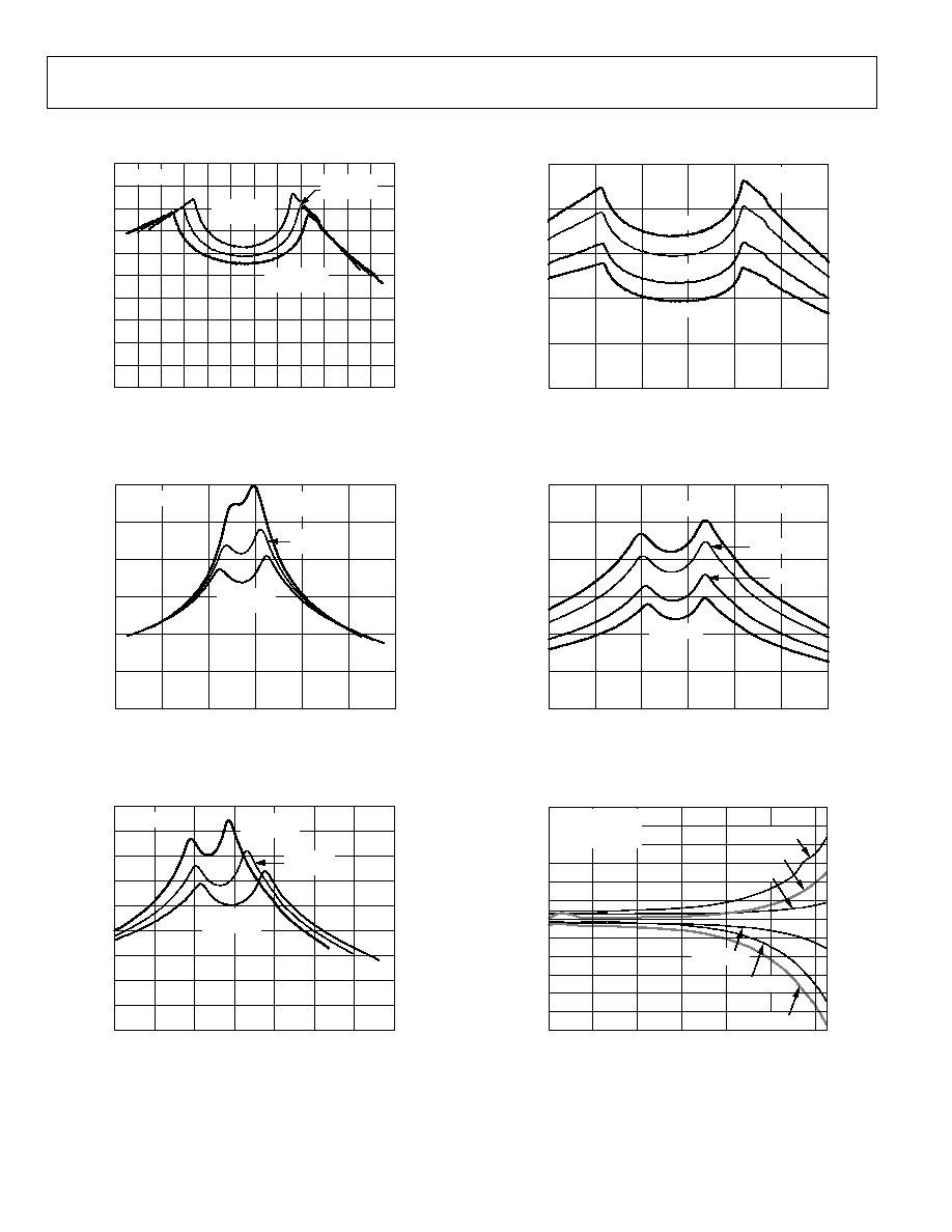
Figure 7. On Resistance as a Function of V
D
(V
S
) for Dual Supply
SOURCE OR DRAIN VOLTAGE (V)
O
N
R
E
SI
ST
A
N
C
E (
)
600
300
0
6
4
2
4
0
2
6
500
400
200
100
T
A
= 25°C
V
DD
= +5V
V
SS
= 5V
V
DD
= +5.5V
V
SS
= 5.5V
V
DD
= +4.5V
V
SS
= 4.5V
0
61
19
-
00
6
Figure 8. On Resistance as a Function of V
D
(V
S
) for Dual Supply
SOURCE OR DRAIN VOLTAGE (V)
O
N
R
ESI
S
T
A
N
C
E
(
)
450
250
300
0
0
2
4
6
12
8
10
14
400
350
150
200
100
50
T
A
= 25°C
V
DD
= 12V
V
SS
= 0V
V
DD
= 13.2V
V
SS
= 0V
V
DD
= 10.8V
V
SS
= 0V
06
11
9-
0
07
Figure 9. On Resistance as a Function of V
D
(V
S
) for Single Supply
SOURCE OR DRAIN VOLTAGE (V)
O
N RE
S
I
S
T
ANCE
(
)
250
0
15
10
5
10
0
5
15
150
200
100
50
T
A
= +25°C
T
A
= +85°C
T
A
= +125°C
T
A
= 40°C
V
DD
= +15V
V
SS
= 15V
06
11
9-
00
8
Figure 10. On Resistance as a Function of V
D
(V
S
) for Different Temperatures,
Dual Supply
SOURCE OR DRAIN VOLTAGE (V)
O
N RE
S
I
S
T
ANCE
(
)
600
0
0
2
4
10
6
8
12
300
400
200
500
100
T
A
= +25°C
T
A
= +85°C
T
A
= +125°C
T
A
= 40°C
V
DD
= 12V
V
SS
= 0V
06
11
9-
0
09
Figure 11. On Resistance as a Function of V
D
(V
S
) for Different Temperatures,
Single Supply
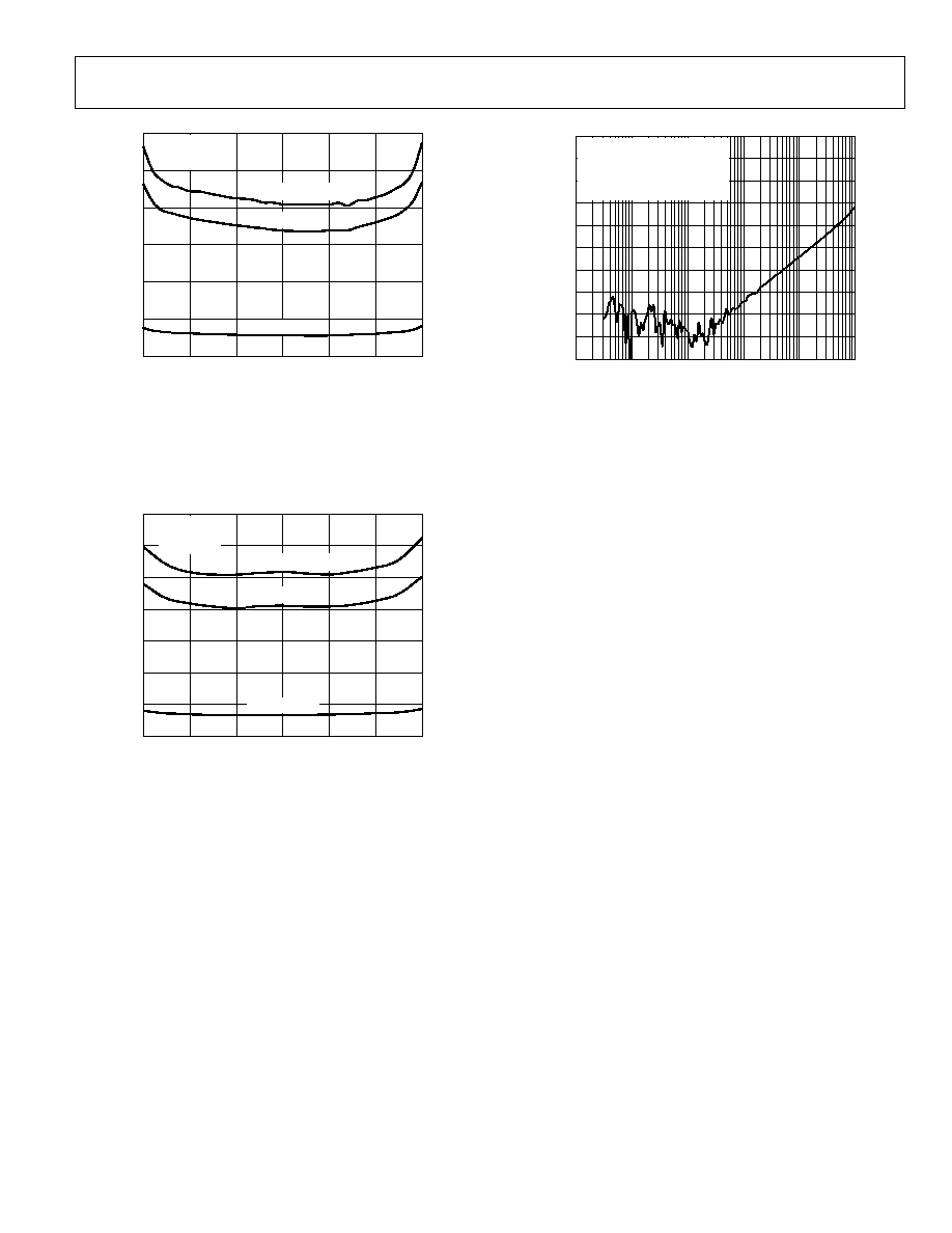
TEMPERATURE (°C)
L
E
AKAG
E
(
p
A
)
1200
1000
800
600
400
200
0
200
400
600
800
1000
1200
0
20
40
100
60
80
120
0
61
19
-
01
0
V
DD
= +15V
V
SS
= 15V
V
BIAS
= +10V/10V
I
S
(OFF) +
I
D
(OFF) +
I
S
(OFF) +
I
D
(OFF) +
I
D
, I
S
(ON) + +
I
D
, I
S
(ON)
Figure 12. ADG1206 Leakage Currents as a Function of Temperature,
Dual Supply
ADG1206/ADG1207
Rev. 0 | Page 13 of 20
TEMPERATURE (°C)
L
E
AKAG
E
(
p
A)
400
400
300
200
100
0
100
200
300
0
20
40
100
60
80
120
0
61
19-
01
1
V
DD
= 12V
V
SS
= 0V
V
BIAS
= 1V/10V
I
S
(OFF) +
I
D
(OFF) +
I
S
(OFF) +
I
D
(OFF) +
I
D
, I
S
(ON )+ +
I
D
, I
S
(ON)
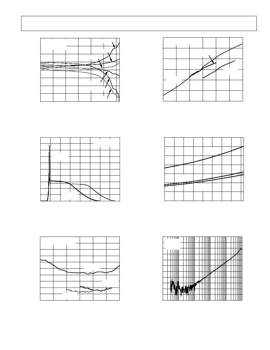
Figure 13. ADG1206 Leakage Currents as a Function of Temperature,
Single Supply
LOGIC, IN
X
(V)
I
DD
(µ
A
)
200
60
80
100
120
140
160
180
40
20
0
0
2
4
6
8
10
12
14
16
V
DD
= +12V
V
SS
= 0V
V
DD
= +15V
V
SS
= 15V
I
DD
PER CHANNEL
T
A
= 25
°C
06
11
9-
01
2
Figure 14. I
DD
vs. Logic Level
V
S
(V)
CH
ARG
E
I
N
JE
CT
I
O
N
(
p
C)
1.0
0
15
15
0.9
0.8
0.7
0.6
0.5
0.4
0.3
0.2
0.1
10
5
0
5
10
MUX (SOURCE TO DRAIN)
T
A
= 25°C
V
DD
= +15V
V
SS
= 15V
V
DD
= +5V
V
SS
= 5V
V
DD
= +12V
V
SS
= 0V
0
61
19
-
0
13
Figure 15. Source-to-Drain Charge Injection vs. Source Voltage
V
S
(V)
CH
ARG
E
I
N
JE
CT
I
O
N
(
p
C)
6
6
15
15
10
5
0
5
10
DEMUX (DRAIN TO SOURCE)
T
A
= 25°C
4
2
0
2
4
V
DD
= +15V
V
SS
= 15V
V
DD
= +5V
V
SS
= 5V
V
DD
= +12V
V
SS
= 0V
0
61
19
-
0
14
Figure 16. Drain-to-Source Charge Injection vs. Source Voltage
350
0
50
100
150
200
250
300
40
20
0
20
40
60
80
100
120
TI
M
E
(
n
s
)
TEMPERATURE (°C)
V
DD
= +5V
V
SS
= 5V
V
DD
= +12V
V
SS
= 0V
V
DD
= +15V
V
SS
= 15V
0
611
9-
0
50
Figure 17. Transition Time vs. Temperature
FREQUENCY (Hz)
O
F
F
I
S
O
L
AT
I
O
N (
d
B)
0
10
20
30
40
50
60
70
80
90
100
110
10k
100k
1M
10M
100M
1G
V
DD
= +15V
V
SS
= 15V
T
A
= 25°C
06
11
9-
0
16
Figure 18. Off Isolation vs. Frequency
ADG1206/ADG1207
Rev. 0 | Page 14 of 20
0
10
20
30
40
50
60
70
80
90
100
110
10k
1G
100M
10M
1M
100k
CRO
S
S
T
A
L
K (
d
B)
FREQUENCY (Hz)
T
A
= 25°C
ADJACENT
CHANNELS
NON ADJACENT
CHANNELS
0
611
9-
0
51
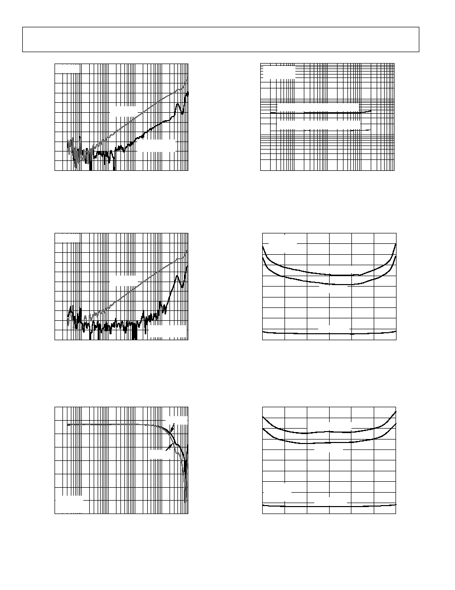
Figure 19. ADG1206 Crosstalk vs. Frequency
0
10
20
30
40
50
60
70
80
90
100
110
10k
1G
100M
10M
1M
100k
CRO
S
S
T
A
L
K (
d
B)
FREQUENCY (Hz)
T
A
= 25°C
ADJACENT
CHANNELS
NON ADJACENT
CHANNELS
0
611
9-
0
52
Figure 20. ADG1207 Crosstalk vs. Frequency
4
20
18
16
14
12
10
8
6
10k
1G
100M
10M
1M
100k
ON
R
E
S
P
ON
S
E
(
d
B
)
FREQUENCY (Hz)
V
DD
= +15V
V
SS
= 15V
T
A
= 25°C
ADG1206
ADG1207
0
611
9-
0
53
Figure 21. On Response vs. Frequency
FREQUENCY (Hz)
T
HD +
N (
%
)
10
1
0.1
0.01
10
100
1k
10k
100k
LOAD = 10k
T
A
= 25°C
V
DD
= +5V, V
SS
= 5V, V
S
= +3.5V rms
V
DD
= +15V, V
SS
= 15V, V
S
= +5V rms
0
61
19
-
0
20
Figure 22. THD + N vs. Frequency
20
0
2
4
6
8
10
12
14
16
18
15
15
5
10
0
5
10
C
AP
A
CI
T
ANC
E
(
p
F
)
V
BIAS
(V)
V
DD
= +15V
V
SS
= 15V
T
A
= 25°C
SOURCE/DRAIN ON
DRAIN OFF
SOURCE OFF
0
61
19-
0
54
Figure 23. ADG1206 Capacitance vs. Source Voltage,
±15 V Dual Supply
20
0
2
4
6
8
10
12
14
16
18
0
1
8
10
6
4
2
CAPAC
I
T
A
NCE (
p
F
)
V
BIAS
(V)
2
V
DD
= 12V
V
SS
= 0V
T
A
= 25°C
SOURCE/DRAIN ON
DRAIN OFF
SOURCE OFF
06
11
9
-
05
5
Figure 24. ADG1206 Capacitance vs. Source Voltage, 12 V Single Supply
ADG1206/ADG1207
Rev. 0 | Page 15 of 20
12
0
2
4
6
8
10
15
15
5
10
0
5
10
CAPAC
I
T
A
NCE (
p
F
)
V
BIAS
(V)
V
DD
= +15V
V
SS
= 15V
T
A
= 25°C
SOURCE/DRAIN ON
DRAIN OFF
SOURCE OFF
0
61
19-
0
56
0
10
20
30
40
50
60
70
80
90
100
100
10M
1M
100k
10k
1k
AC
P
S
RR
(
d
B
)
FREQUENCY (Hz)
T
A
= 25°C
NO DECOUPLING CAPACITORS
V
DD
= +15V
V
SS
= 15V
V p-p = 0.63V
06
11
9-
05
8
Figure 25. ADG1207 Capacitance vs. Source Voltage, ±15 V Dual Supply
Figure 27. AC PSRR vs. Frequency
14
12
0
2
4
6
8
10
0
1
8
10
6
4
2
C
A
PA
C
I
T
A
N
C
E (
p
F
)
V
BIAS
(V)
2
V
DD
= 12V
V
SS
= 0V
T
A
= 25°C
SOURCE/DRAIN ON
DRAIN OFF
SOURCE OFF
06
11
9
-
05
7
Figure 26. ADG1207 Capacitance vs. Source Voltage, 12 V Single Supply

ADG1206/ADG1207
Rev. 0 | Page 16 of 20
TERMINOLOGY
R
ON
Ohmic resistance between D and S.
R
ON
Difference between the R
ON
of any two channels.
R
FLAT(ON)
Flatness is defined as the difference between the maximum and
minimum value of on resistance as measured.
I
S
(Off)
Source leakage current when the switch is off.
I
D
(Off)
Drain leakage current when the switch is off.
I
D
, I
S
(On)
Channel leakage current when the switch is on.
V
D
(V
S
)
Analog voltage on Terminals D and S.
C
S
(Off)
Channel input capacitance for the off condition.
C
D
(Off)
Channel output capacitance for the off condition.
C
D
, C
S
(On)
On switch capacitance.
C
IN
Digital input capacitance.
t
ON
(EN)
Delay time between the 50% and 90% points of the digital input
and the switch on condition.
t
OFF
(EN)
Delay time between the 50% and 90% points of the digital input
and the switch off condition.
t
TRANSITION
Delay time between the 50% and 90% points of the digital
inputs and the switch on condition when switching from one
address state to another.
T
BBM
Off time measured between the 80% points of the switches
when switching from one address state to another.
V
INL
Maximum input voltage for Logic 0.
V
INH
Minimum input voltage for Logic 1.
I
INL
(I
INH
)
Input current of the digital input.
I
DD
Positive supply current.
I
SS
Negative supply current.
Off Isolation
A measure of unwanted signal coupling through an off channel.
Charge Injection
A measure of the glitch impulse transferred from the digital
input to the analog output during switching.
Bandwidth
The frequency at which the output is attenuated by 3 dB.
On Response
The frequency response of the on switch.
THD + N
The ratio of the harmonic amplitude plus noise of the signal to
the fundamental.
ACPSRR (AC Power Supply Rejection Ratio)
Measures the ability of a part to avoid coupling noise and
spurious signals that appear on the supply voltage pin to the
output of the switch. The dc voltage on the device is modulated
by a sine wave of 0.62 V p-p. The ratio of the amplitude of
signal on the output to the amplitude of the modulation is the
ACPSRR.
ADG1206/ADG1207
Rev. 0 | Page 17 of 20
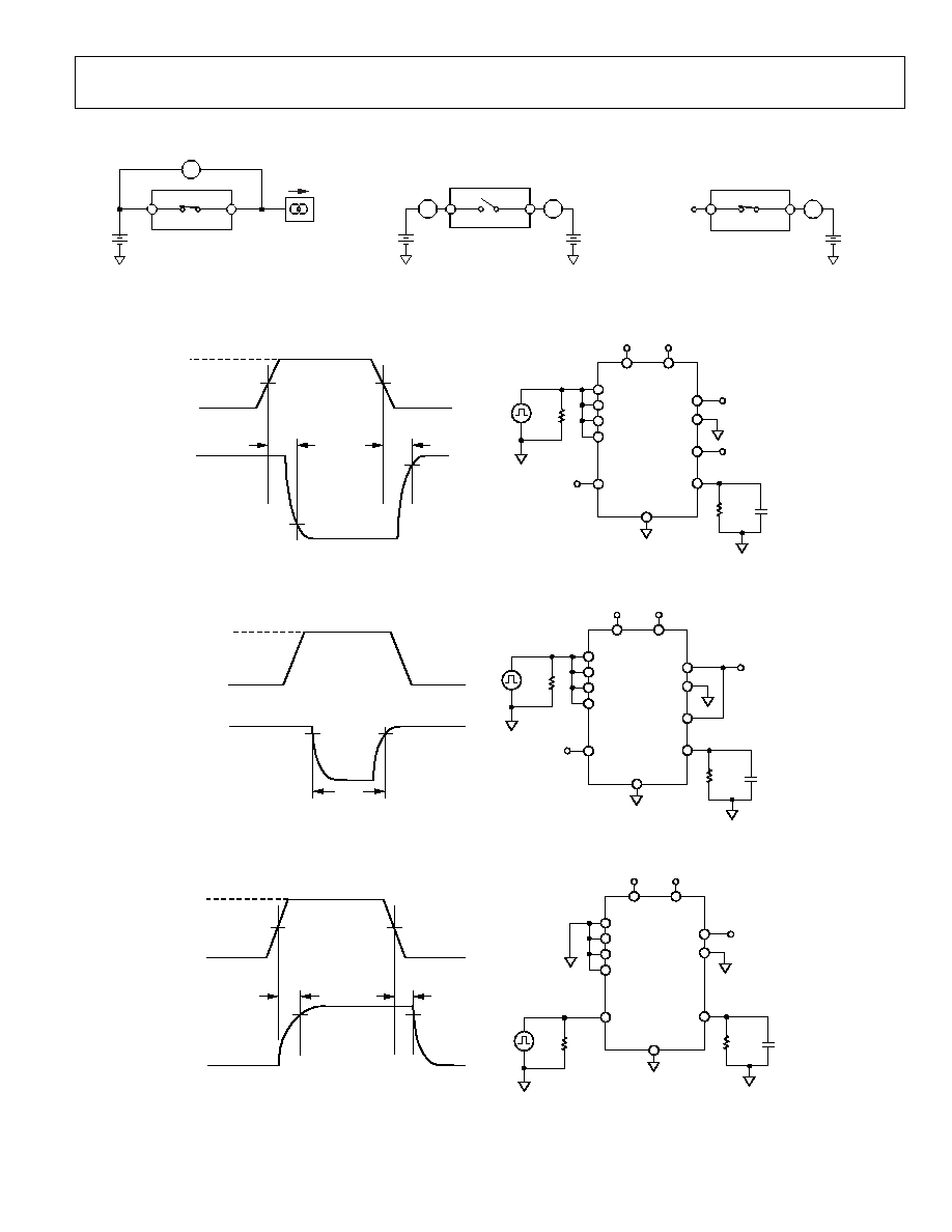
TEST CIRCUITS
I
DS
S
D
V
S
V
061
19-
02
5
S
D
V
S
A
A
V
D
I
S
(OFF)
I
D
(OFF)
061
19-
02
6
S
D
A
V
D
I
D
(ON)
NC
NC = NO CONNECT
061
19-
02
7
Figure 28. On Resistance
Figure 29. Off Leakage
Figure 30. On Leakage
3V
0V
OUTPUT
t
r < 20ns
t
f < 20ns
ADDRESS
DRIVE (V
IN
)
t
TRANSITION
t
TRANSITION
50%
50%
90%
90%
OUTPUT
ADG1206
1
50
300
GND
S1
S2 TO S15
S16
D
35pF
V
IN
2.4V
EN
V
DD
V
SS
V
DD
V
SS
V
S1
V
S16
1
SIMILAR CONNECTION FOR ADG1207.
A0
A2
A1
A3
06
11
9-
0
2
8
Figure 31. Address to Output Switching Times, t
TRANSITION
3V
0V
OUTPUT
80%
80%
ADDRESS
DRIVE (V
IN
)
t
BBM
OUTPUT
ADG1206
1
50
300
GND
S1
S2 TO S15
S16
D
35pF
V
IN
2.4V
EN
V
DD
V
SS
V
DD
V
SS
V
S
1
SIMILAR CONNECTION FOR ADG1207.
A0
A2
A1
A3
0
611
9-
0
29
Figure 32. Break-Before-Make Delay, t
BBM
3V
0V
OUTPUT
50%
50%
t
OFF
(EN)
t
ON
(EN)
0.9V
O
0.9V
O
ENABLE
DRIVE (V
IN
)
OUTPUT
ADG1206
1
300
GND
S1
S2 TO S16
D
35pF
50
V
IN
EN
V
DD
V
SS
V
DD
V
SS
V
S
1
SIMILAR CONNECTION FOR ADG1207.
A0
A2
A1
A3
06
11
9-
03
0
Figure 33. Enable Delay, t
ON
(EN), t
OFF
(EN)
ADG1206/ADG1207
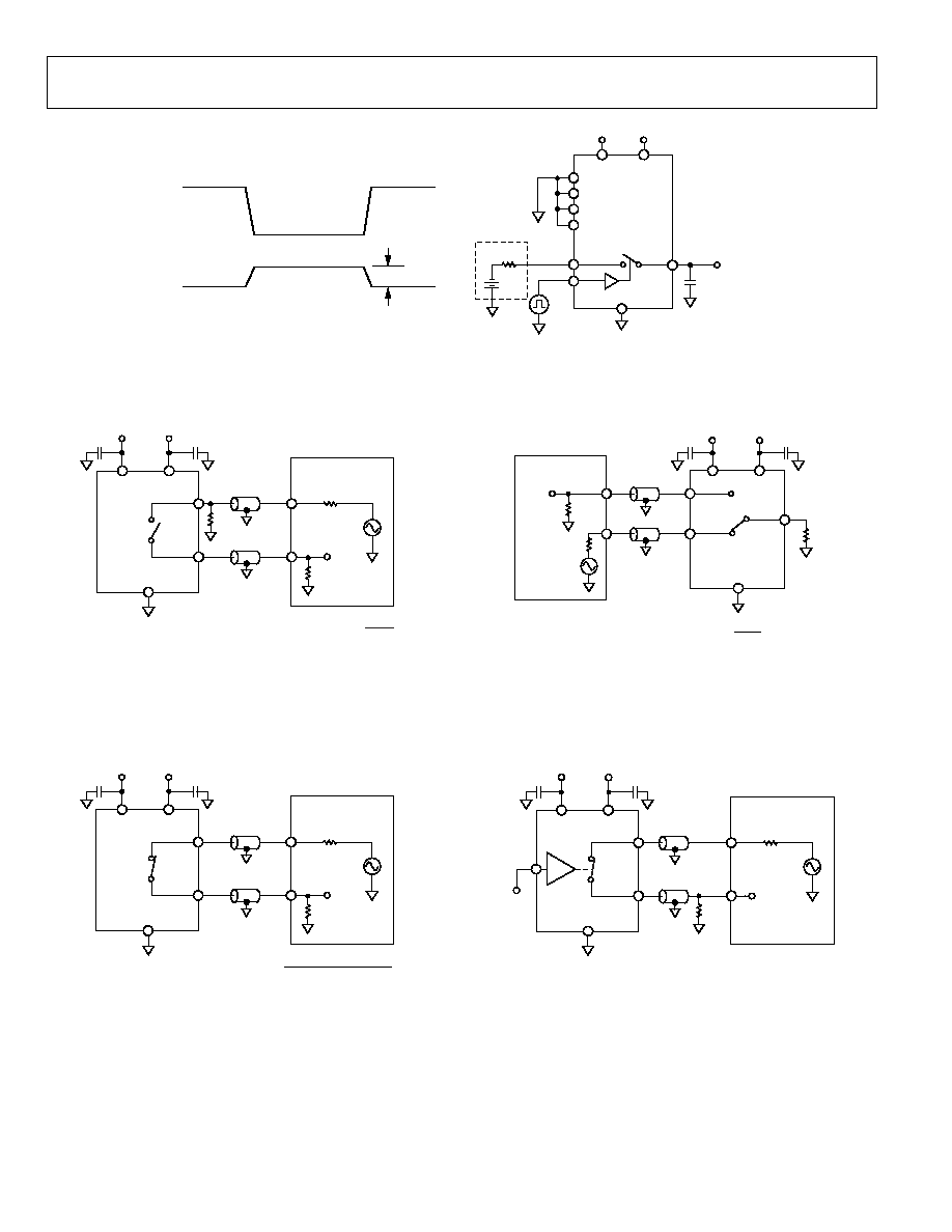
Rev. 0 | Page 18 of 20
3V
V
IN
V
OUT
Q
INJ
= C
L
× V
OUT
V
OUT
V
IN
ADG1206
1
GND
V
DD
V
SS
V
DD
V
SS
1
SIMILAR CONNECTION FOR ADG1207.
A0
D
C
L
1nF
V
OUT
A2
A1
A3
S
EN
R
S
V
S
061
19
-
0
31
Figure 34. Charge Injection
V
OUT
50
NETWORK
ANALYZER
R
L
50
S
D
50
OFF ISOLATION = 20 log
V
OUT
V
S
V
S
V
DD
V
SS
0.1µF
V
DD
0.1µF
V
SS
GND
0
61
19
-
03
2
Figure 35. Off Isolation
V
OUT
50
NETWORK
ANALYZER
R
L
50
S
D
V
S
V
DD
V
SS
0.1µF
V
DD
0.1µF
V
SS
GND
INSERTION LOSS = 20 log
V
OUT
WITH SWITCH
V
OUT
WITHOUT SWITCH
06
11
9-
0
33
Figure 36. Bandwidth
CHANNEL-TO-CHANNEL CROSSTALK = 20 log
V
OUT
GND
S1
D
S2
V
OUT
NETWORK
ANALYZER
R
L
50
R
50
V
S
V
S
V
DD
V
SS
0.1µF
V
DD
0.1µF
V
SS
0
611
9-
0
34
Figure 37. Channel-to-Channel Crosstalk
V
OUT
R
S
AUDIO PRECISION
R
L
10k
IN
V
IN
S
D
V
S
V p-p
V
DD
V
SS
0.1µF
V
DD
0.1µF
V
SS
GND
0
611
9-
03
5
Figure 38. THD + Noise
ADG1206/ADG1207
Rev. 0 | Page 19 of 20
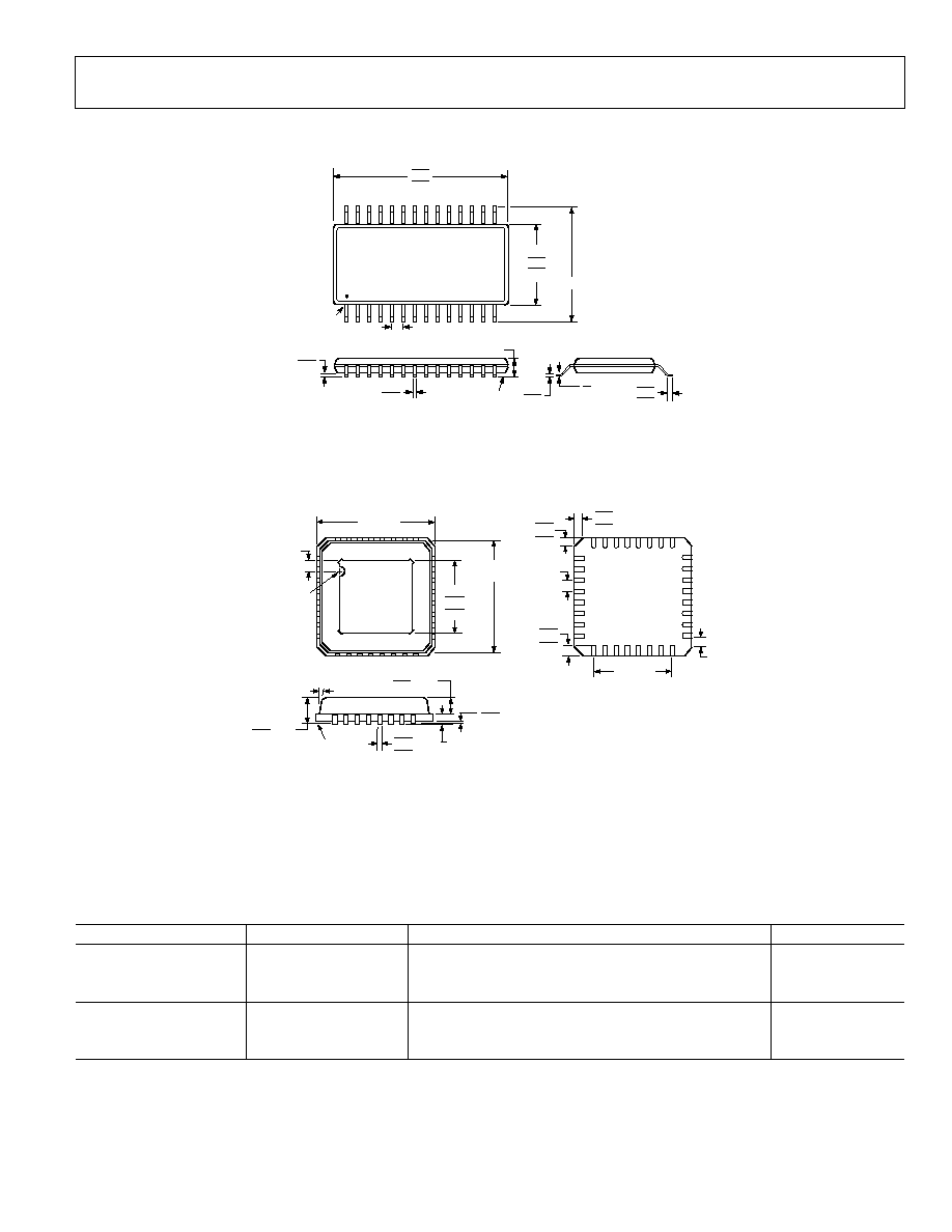
OUTLINE DIMENSIONS
COMPLIANT TO JEDEC STANDARDS MO-153-AE
2 8
1 5
1 4
1
8 °
0 °
SEATING
PLANE
COPLANARITY
0.10
1.20 MAX
6.40 BSC
0.65
BSC
PIN 1
0.30
0.19
0.20
0.09
4.50
4.40
4.30
0.75
0.60
0.45
9.80
9.70
9.60
0.15
0.05
Figure 39. 28-Lead Thin Shrink Small Outline Package [TSSOP]
(RU-28)
Dimensions shown in millimeters
*COMPLIANT TO JEDEC STANDARDS MO-220
WITH EXCEPTION TO PADDLE ORIENTATION.
0.30
0.23
0.18
0.20 REF
0.80 MAX
0.65 TYP
0.05 MAX
0.02 NOM
12° MAX
1.00 MAX
0.85 NOM
SEATING
PLANE
COPLANARITY
0.05
1
32
8
9
25
24
16
17
BOTTOM
VIEW
2.85
2.70 SQ
2.55
0.50
0.40
0.30
0.60
0.42
0.24
0.60
0.42
0.24
3.50 REF
0.50
BSC
PIN 1
INDICATOR
5.00
BSC SQ
4.75
BSC SQ
0.45
BSC
0.20
MIN
*EXPOSED
PAD
(TOP VIEW)
Figure 40. 32-Lead Lead Frame Chip Scale Package [LFCSP_VQ]
5 mm × 5 mm Body, Very Thin Quad
(CP-32-2)
Dimensions shown in millimeters
ORDERING GUIDE
Model
Temperature Range
Description
Package Option
ADG1206YRUZ
1
-40°C to +125°C
28-Lead Thin Shrink Small Outline Package [TSSOP]
RU-28
ADG1206YRUZ-REEL7
1
-40°C to +125°C
28-Lead Thin Shrink Small Outline Package [TSSOP]
RU-28
ADG1206YCPZ-REEL7
1
-40°C to +125°C
32-Lead Lead Frame Chip Scale Package [LFCSP_VQ]
CP-32-2
ADG1207YRUZ
1
-40°C to +125°C
28-Lead Thin Shrink Small Outline Package [TSSOP]
RU-28
ADG1207YRUZ-REEL7
1
-40°C to +125°C
28-Lead Thin Shrink Small Outline Package [TSSOP]
RU-28
ADG1207YCPZ-REEL7
1
-40°C to +125°C
32-Lead Lead Frame Chip Scale Package [LFCSP_VQ]
CP-32-2
1
Z = Pb-free part.

ADG1206/ADG1207
Rev. 0 | Page 20 of 20
NOTES
©2006 Analog Devices, Inc. All rights reserved. Trademarks and
registered trademarks are the property of their respective owners.
D06119-0-7/06(0)
Document Outline
- þÿ
- þÿ
- þÿ
- þÿ
- þÿ
- þÿ
- þÿ
- þÿ
- þÿ
- þÿ
- þÿ
- þÿ