 | ÐлекÑÑоннÑй компоненÑ: ADF4107 | СкаÑаÑÑ:  PDF PDF  ZIP ZIP |
Äîêóìåíòàöèÿ è îïèñàíèÿ www.docs.chipfind.ru
PLL Frequency Synthesizer
ADF4107
FEATURES
7.0 GHz bandwidth
2.7 V to 3.3 V power supply
Separate charge pump supply (V
P
) allows extended tuning
voltage in 3 V systems
Programmable dual-modulus prescaler
8/9, 16/17, 32/33, 64/65
Programmable charge pump currents
Programmable antibacklash pulsewidth
3-wire serial interface
Analog and digital lock detect
Hardware and software power-down mode
APPLICATIONS
Broadband wireless access
Satellite systems
Instrumentation
Wireless LANs
Base stations for wireless radio
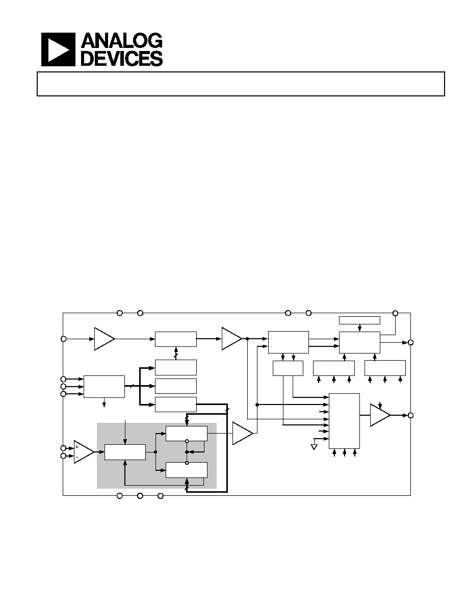
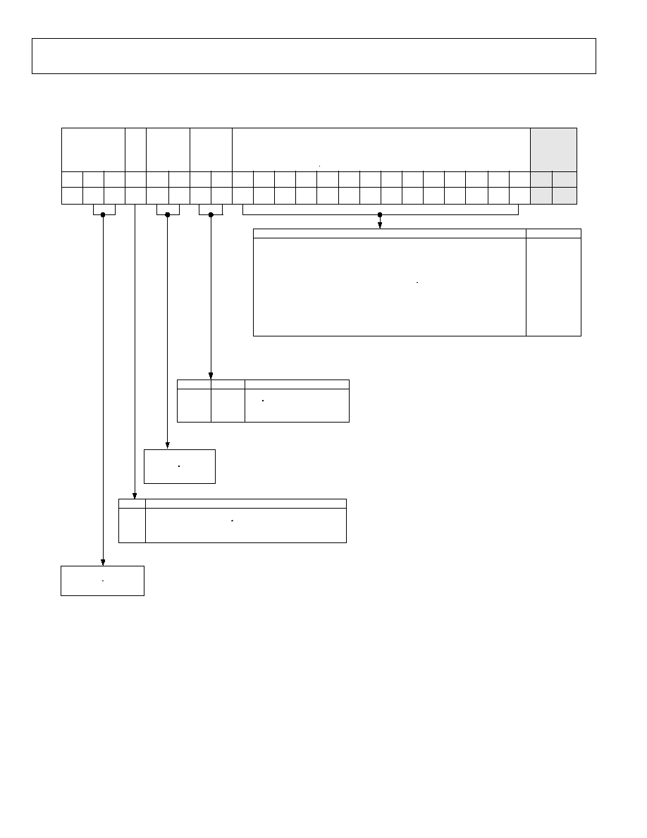
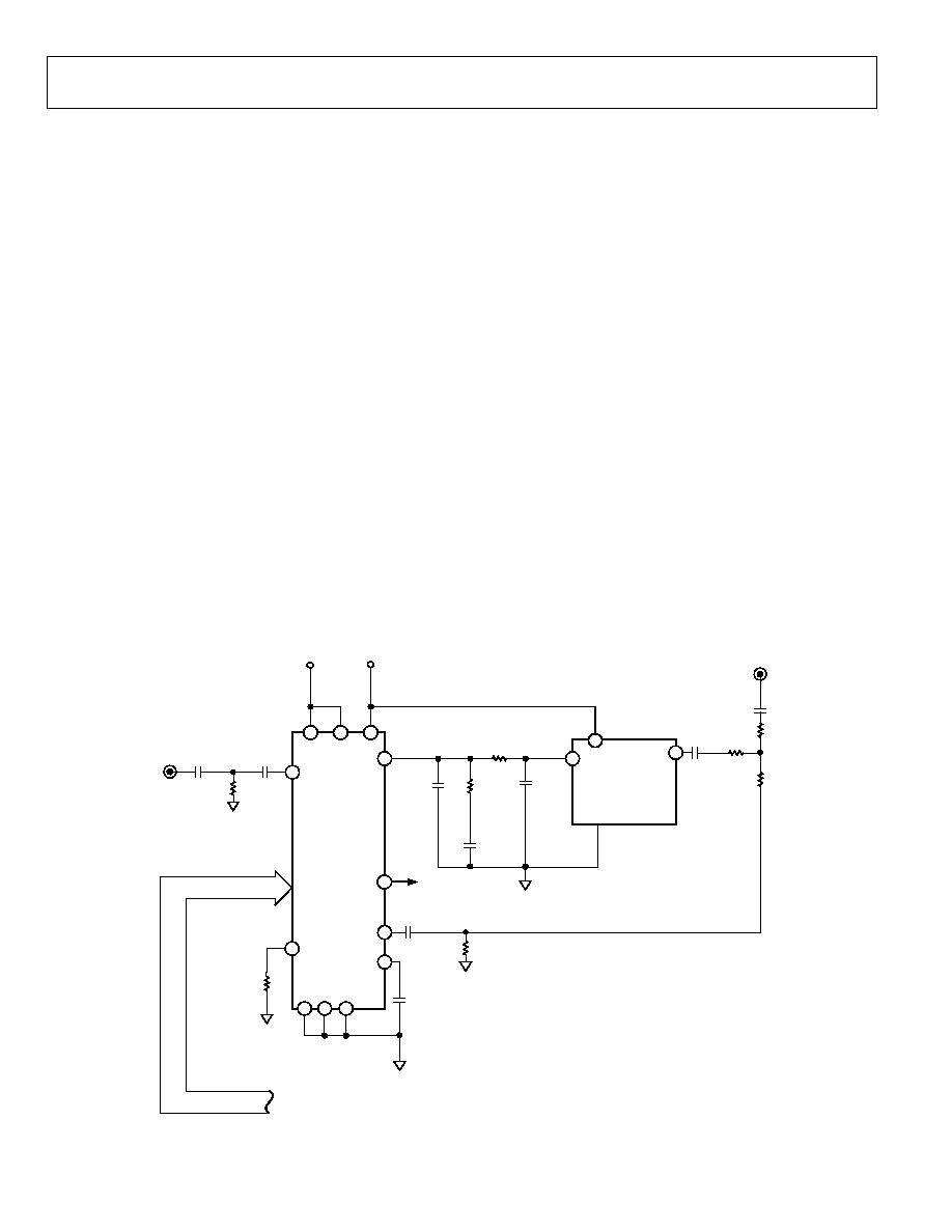
GENERAL DESCRIPTION
The ADF4107 frequency synthesizer can be used to implement
local oscillators in the up-conversion and down-conversion
sections of wireless receivers and transmitters. It consists of a
low-noise digital PFD (phase frequency detector), a precision
charge pump, a programmable reference divider, programmable
A and B counters, and a dual-modulus prescaler (P/P + 1). The
A (6-bit) and B (13-bit) counters, in conjunction with the dual-
modulus prescaler (P/P + 1), implement an N divider
(N = BP + A). In addition, the 14-bit reference counter
(R counter), allows selectable REFIN frequencies at the PFD
input. A complete PLL (phase-locked loop) can be implemented
if the synthesizer is used with an external loop filter and VCO
(voltage controlled oscillator). Its very high bandwidth means
that frequency doublers can be eliminated in many high
frequency systems, simplifying system architecture and
reducing cost.
FUNCTIONAL BLOCK DIAGRAM
CLK
DATA
LE
REF
IN
RF
IN
A
RF
IN
B
24-BIT INPUT
REGISTER
SD
OUT
AV
DD
DV
DD
CE
AGND DGND
14-BIT
R COUNTER
R COUNTER
LATCH
22
14
FUNCTION
LATCH
A, B COUNTER
LATCH
FROM
FUNCTION
LATCH
PRESCALER
P/P + 1
N = BP + A
LOAD
LOAD
13-BIT
B COUNTER
6-BIT
A COUNTER
6
19
13
M3 M2 M1
MUX
SD
OUT
AV
DD
HIGH Z
MUXOUT
CPGND
R
SET
V
P
CP
PHASE
FREQUENCY
DETECTOR
LOCK
DETECT
REFERENCE
CHARGE
PUMP
CURRENT
SETTING 1
ADF4107
CPI3 CPI2 CPI1
CPI6 CPI5 CPI4
CURRENT
SETTING 2
Figure 1.
Rev. 0
Information furnished by Analog Devices is believed to be accurate and reliable.
However, no responsibility is assumed by Analog Devices for its use, nor for any
infringements of patents or other rights of third parties that may result from its use.
Specifications subject to change without notice. No license is granted by implication
or otherwise under any patent or patent rights of Analog Devices. Trademarks and
registered trademarks are the property of their respective companies.
One Technology Way, P.O. Box 9106, Norwood, MA 02062-9106, U.S.A.
Tel: 781.329.4700
www.analog.com
Fax: 781.326.8703
© 2003 Analog Devices, Inc. All rights reserved.

ADF4107
TABLE OF CONTENTS
ADF4107--Specifications................................................................ 3
Timing Characteristics..................................................................... 5
Absolute Maximum Ratings............................................................ 5
Pin Configurations and Functional Descriptions ........................ 6
Typical Performance Characteristics ............................................. 7
Functional Description .................................................................... 9
Reference Input Stage................................................................... 9
RF Input Stage............................................................................... 9
Prescaler (P/P + 1)........................................................................ 9
A and B Counters ......................................................................... 9
R Counter ...................................................................................... 9
Phase Frequency Detector and Charge Pump........................ 10
MUXOUT and Lock Detect...................................................... 10
Input Shift Register..................................................................... 10
Latch Summary........................................................................... 11
Reference Counter Latch Map.................................................. 12
AB Counter Latch Map ............................................................. 13
Function Latch Map................................................................... 14
Initialization Latch Map ............................................................ 15
Function Latch............................................................................ 16
Initialization Latch ..................................................................... 17
Applications..................................................................................... 18
Local Oscillator for LMDS Base Station Transmitter............ 18
Interfacing ................................................................................... 19
PCB Design Guidelines for Chip Scale Package .................... 19
Outline Dimensions ....................................................................... 20
ESD Caution.................................................................................... 20
Ordering Guide............................................................................... 20
REVISION HISTORY
Revision 0: Initial Version
Rev. 0 | Page 2 of 20

ADF4107
ADF4107--SPECIFICATIONS
Table 1. (AV
DD
= DV
DD
= 3 V ± 10%, AV
DD
V
P
5.5 V, AGND = DGND = CPGND = 0 V, R
SET
= 5.1 k, dBm referred to 50 , T
A
=
T
MAX
to T
MIN
, unless otherwise noted.)
Parameter B
Version
1
B Chips
2
(Typ)
Unit Test
Conditions/Comments
RF CHARACTERISTICS
RF Input Frequency (RF
IN
)
3
1.0/7.0
1.0/7.0
GHz min/max
See Figure 18 for input circuit.
RF Input Sensitivity
5/+5
5/+5
dBm min/max
Maximum Allowable Prescaler
Output Frequency
4
300 300
MHz
max
REFIN CHARACTERISTICS
REFIN Input Frequency
20/250
20/250
MHz min/max
For f < 20 MHz, use dc-coupled square wave (0 to V
DD
).
REFIN Input Sensitivity
5
0.8/V
DD
0.8/V
DD
V p-p min/max
AC-coupled; when dc-coupled, 0 to V
DD
, max (CMOS
compatible).
REFIN Input Capacitance
10
10
pF max
REFIN Input Current
±100
±100
µA max
PHASE DETECTOR
Phase Detector Frequency
6
104 104 MHz
max
CHARGE PUMP
Programmable; see Figure 25.
I
CP
Sink/Source
High Value
5
5
mA typ
With R
SET
= 5.1 k
Low Value
625
625
µA typ
Absolute Accuracy
2.5
2.5
% typ
With R
SET
= 5.1 k
R
SET
Range
3.0/11
3.0/11
k typ
See Figure 25.
I
CP
Three-State Leakage
1
1
nA typ
Sink and Source Current
Matching
2
2
% typ
0.5 V V
CP
V
P
0.5 V
I
CP
vs. V
CP
1.5
1.5
% typ
0.5 V V
CP
V
P
0.5 V
I
CP
vs. Temperature
2
2
% typ
V
CP
= V
P
/2
LOGIC INPUTS
V
IH
, Input High Voltage
1.4
1.4
V min
V
IL
, Input Low Voltage
0.6
0.6
V max
I
INH
, I
INL
, Input Current
±1
±1
µA max
C
IN
, Input Capacitance
10
10
pF max
LOGIC OUTPUTS
V
OH
, Output High Voltage
1.4
1.4
V min
Open-drain output chosen; 1 k pull-up resistor to 1.8 V.
V
OH
, Output High Voltage
V
DD
0.4
V
DD
0.4
V min
CMOS output chosen.
I
OH
100
100
µA
max
V
OL
, Output Low Voltage
0.4
0.4
V max
I
OL
= 500 µA
POWER SUPPLIES
AV
DD
2.7/3.3
2.7/3.3
V min/V max
DV
DD
AV
DD
AV
DD
V
P
AV
DD
/5.5 AV
DD
/5.5
V min/V max
AV
DD
V
P
5.5V
I
DD
7
(AI
DD
+ DI
DD
)
17
15
mA max
15 mA typ
I
P
0.4
0.4
mA
max
T
A
= 25°C
Power-Down Mode
8
(AI
DD
+ DI
DD
) 10
10
µA
typ
Rev. 0 | Page 3 of 20

ADF4107
Rev. 0 | Page 4 of 20
Parameter B
Version
1
B Chips
2
(Typ)
Unit Test
Conditions/Comments
NOISE CHARACTERISTICS
ADF4107 Phase Noise Floor
9
174
174
dBc/Hz typ
@ 25 kHz PFD Frequency
166
166
dBc/Hz typ
@ 200 kHz PFD Frequency
159
159
dBc/Hz typ
@ 1 MHz PFD Frequency
Phase Noise Performance
10
@ VCO Output
900 MHz Output
11
93
93
dBc/Hz typ
@ 1 kHz offset and 200 kHz PFD Frequency
6400 MHz Output
12
76
76
dBc/Hz typ
@ 1 kHz offset and 200 kHz PFD Frequency
6400 MHz Output
13
83
83
dBc/Hz typ
@ 1 kHz offset and 1 MHz PFD Frequency
Spurious Signals
900 MHz Output
11
90/92
90/92
dBc typ
@ 200 kHz/400kHz and 200 kHz PFD Frequency
6400 MHz Output
12
65/70
65/70
dBc typ
@ 200 kHz/400kHz and 200 kHz PFD Frequency
6400 MHz Output
13
70/75
70/75
dBc typ
@ 1 MHz/2MHz and 1 MHz PFD Frequency
1
Operating temperature range (B Version) is 40°C to +85°C.
2
The B Chip specifications are given as typical values.
3
Use a square wave for lower frequencies, below the minimum stated.
4
This is the maximum operating frequency of the CMOS counters. The prescaler value should be chosen to ensure that the RF input is divided down to a frequency that
is less than this value.
5
AV
DD
= DV
DD
= 3 V.
6
Guaranteed by design. Sample tested to ensure compliance.
7
T
A
= 25°C; AV
DD
= DV
DD
= 3 V; P = 32; RF
IN
= 7.0 GHz.
8
T
A
= 25°C; AV
DD
= DV
DD
= 3.3 V; R = 16383; A = 63; B = 891; P = 32; RF
IN
= 7.0 GHz.
9
The synthesizer phase noise floor is estimated by measuring the in-band phase noise at the output of the VCO and subtracting 20logN (where N is the N divider value).
10
The phase noise is measured with the EVAL-ADF4107EB1 Evaluation Board and the HP8562E Spectrum Analyzer. The spectrum analyzer provides the REFIN for the
synthesizer (f
REFOUT
= 10 MHz @ 0 dBm).
11
f
REFIN
= 10 MHz; f
PFD
= 200 kHz; Offset Frequency = 1 kHz; f
RF
= 900 MHz; N = 4500; Loop B/W = 20 kHz.
12
f
REFIN
= 10 MHz; f
PFD
= 200 kHz; Offset Frequency = 1 kHz; f
RF
= 6400 MHz; N = 32000; Loop B/W = 20 kHz.
13
f
REFIN
= 10 MHz; f
PFD
= 1 MHz; Offset Frequency = 1 kHz; f
RF
= 6400 MHz; N = 6400; Loop B/W = 100 kHz.
ADF4107
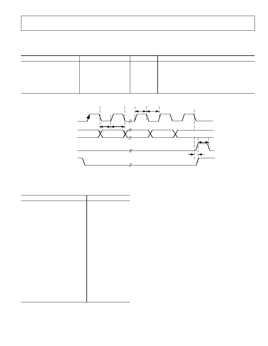
TIMING CHARACTERISTICS
Table 2. (AV
DD
= DV
DD
= 3 V ± 10%, AV
DD
V
P
5.5 V, AGND = DGND = CPGND = 0 V, R
SET
= 5.1 k, dBm referred to 50 ,
T
A
= T
MAX
to T
MIN
, unless otherwise noted.)
1
Parameter Limit
2
(B Version)
Unit
Test Conditions/Comments
t
1
10
ns min
DATA to CLOCK Setup Time
t
2
10
ns min
DATA to CLOCK Hold Time
t
3
25
ns min
CLOCK High Duration
t
4
25
ns min
CLOCK Low Duration
t
5
10
ns min
CLOCK to LE Setup Time
t
6
20
ns min
LE Pulsewidth
1
Guaranteed by design but not production tested.
2
Operating temperature range (B Version) is 40°C to +85°C.
CLOCK
DB22
DB2
DATA
LE
t
1
LE
DB23 (MSB)
t
2
DB1 (CONTROL
BIT C2)
DB0 (LSB)
(CONTROL BIT C1)
t
3
t
4
t
6
t
5
Figure 2. Timing Diagram
ABSOLUTE MAXIMUM RATINGS
Table 3. (T
A
= 25°C, unless otherwise noted.)
Parameter Rating
AV
DD
to GND
1
0.3 V to +3.6 V
AV
DD
to DV
DD
0.3 V to +0.3 V
V
P
to GND
0.3 V to +5.8 V
V
P
to AV
DD
0.3 V to +5.8 V
Digital I/O Voltage to GND
0.3 V to V
DD
+ 0.3 V
Analog I/O Voltage to GND
0.3 V to V
P
+ 0.3 V
REFIN, RF
IN
A, RF
IN
B to GND
0.3 V to V
DD
+ 0.3 V
Operating Temperature Range
Industrial (B Version)
40°C to +85°C
Storage Temperature Range
65°C to +125°C
Maximum Junction Temperature
150°C
TSSOP
JA
Thermal Impedance
150.4°C/W
CSP
JA
Thermal Impedance
122°C/W
Lead Temperature, Soldering
Vapor Phase (60 sec)
215°C
Infrared (15 sec)
220°C
Transistor Count
CMOS 6425
Bipolar 303
Stresses above those listed under Absolute Maximum Ratings
may cause permanent damage to the device. This is a stress
rating only; functional operation of the device at these or any
other conditions above those listed in the operational sections
of this specification is not implied. Exposure to absolute
maximum rating conditions for extended periods may affect
device reliability.
This device is a high performance RF integrated circuit with an
ESD rating of <2 kV, and it is ESD sensitive. Proper precautions
should be taken for handling and assembly.
1
GND = AGND = DGND = 0 V.
Rev. 0 | Page 5 of 20
ADF4107
Rev. 0 | Page 6 of 20
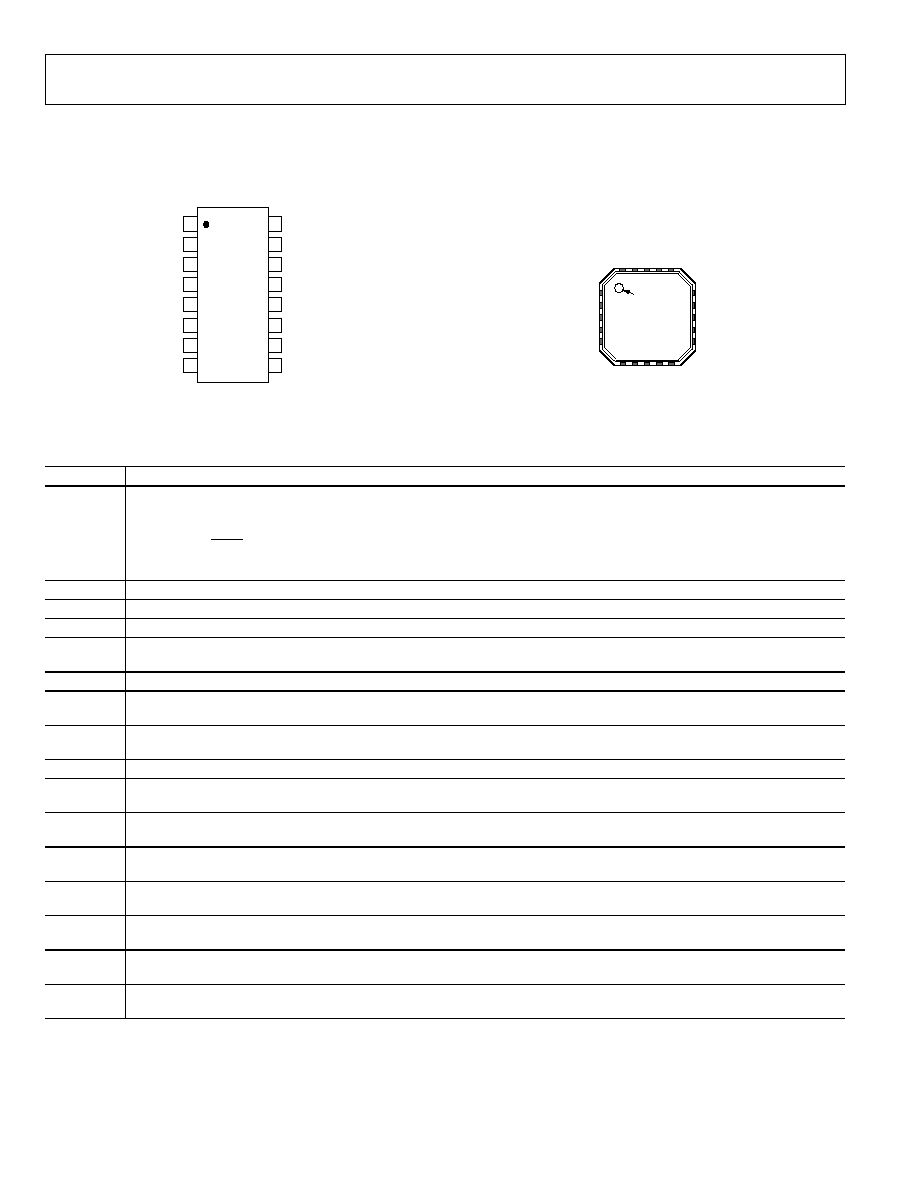
PIN CONFIGURATIONS AND FUNCTIONAL DESCRIPTIONS
R
SET
CP
CPGND
AGND
MUXOUT
LE
DATA
CLK
CE
DGND
16
15
14
13
12
11
10
9
1
2
3
4
5
6
7
8
RF
IN
B
RF
IN
A
AV
DD
REF
IN
V
P
DV
DD
ADF4107
TOP VIEW
(Not to Scale)
TSSOP
Figure 3. ADF4107 TSSOP (Top View)
15 MUXOUT
14 LE
13 DATA
12 CLK
CPGND 1
AGND 2
AGND 3
20 C
P
11 CE
6
7
8
DG
ND 9
DG
ND 1
0
4
5
19
18
17
16
RF
IN
B
RF
IN
A
R
SET
V
P
DV
DD
DV
DD
PIN 1
INDICATOR
TOP VIEW
ADF4107
AV
DD
AV
DD
REF
IN
CSP
(Chip Scale Package)
Figure 4. ADF4107 Chip Scale Package
Table 4. Pin Functional Descriptions
Mnemonic Function
R
SET
Connecting a resistor between this pin and CPGND sets the maximum charge pump output current. The nominal voltage
potential at the R
SET
pin is 0.66 V. The relationship between I
CP
and R
SET
is
SET
MAX
CP
R
I
5
.
25
=
so, with R
SET
= 5.1 k, I
CP MAX
= 5 mA.
CP
Charge Pump Output. When enabled, this pin provides ±I
CP
to the external loop filter, which in turn drives the external VCO.
CPGND
Charge Pump Ground. This is the ground return path for the charge pump.
AGND
Analog Ground. This is the ground return path of the prescaler.
RF
IN
B
Complementary Input to the RF Prescaler. This point must be decoupled to the ground plane with a small bypass capacitor,
typically 100 pF. See Figure 18.
RF
IN
A
Input to the RF Prescaler. This small signal input is ac-coupled to the external VCO.
AV
DD
Analog Power Supply. This voltage may range from 2.7 V to 3.3 V. Decoupling capacitors to the analog ground plane should
be placed as close as possible to this pin. AV
DD
must be the same value as DV
DD
.
REF
IN
Reference Input. This is a CMOS input with a nominal threshold of V
DD
/2 and a dc equivalent input resistance of 100 k. See
Figure 17. This input can be driven from a TTL or CMOS crystal oscillator or it can be ac-coupled.
DGND Digital
Ground.
CE
Chip Enable. A logic low on this pin powers down the device and puts the charge pump output into three-state mode. Taking
the pin high will power up the device, depending on the status of the power-down bit, F2.
CLK
Serial Clock Input. This serial clock is used to clock in the serial data to the registers. The data is latched into the 24-bit shift
register on the CLK rising edge. This input is a high impedance CMOS input.
DATA
Serial Data Input. The serial data is loaded MSB first with the two LSBs being the control bits. This input is a high impedance
CMOS input.
LE
Load Enable, CMOS Input. When LE goes high, the data stored in the shift registers is loaded into one of the four latches, the
latch being selected using the control bits.
MUXOUT
This multiplexer output allows either the lock detect, the scaled RF, or the scaled reference frequency to be accessed
externally.
DV
DD
Digital Power Supply. This may range from 2.7 V to 3.3 V. Decoupling capacitors to the digital ground plane should be placed
as close as possible to this pin. DV
DD
must be the same value as AV
DD
.
V
P
Charge Pump Power Supply. This voltage should be greater than or equal to V
DD
. In systems where V
DD
is 3 V, it can be set to 5
V and used to drive a VCO with a tuning range of up to 5 V.
ADF4107
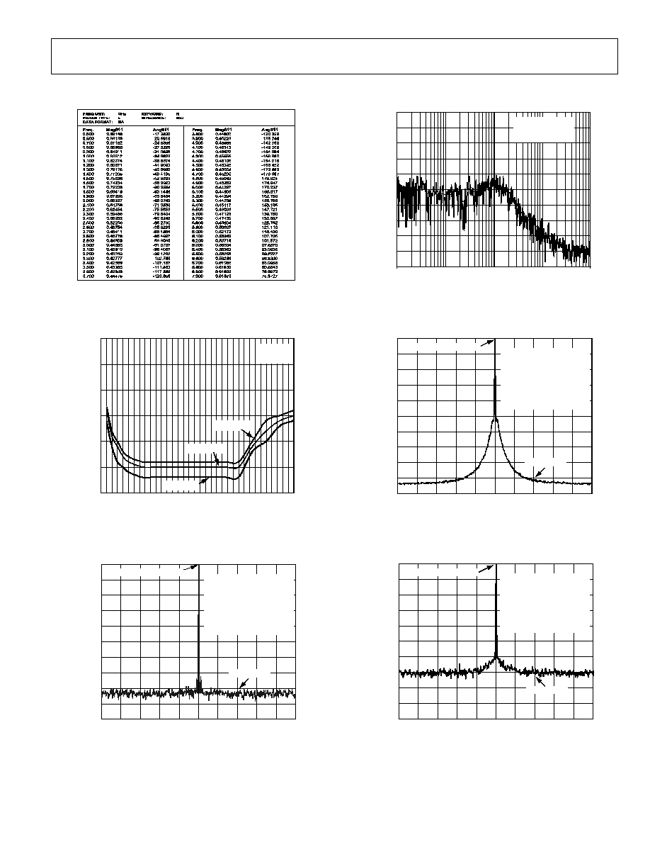
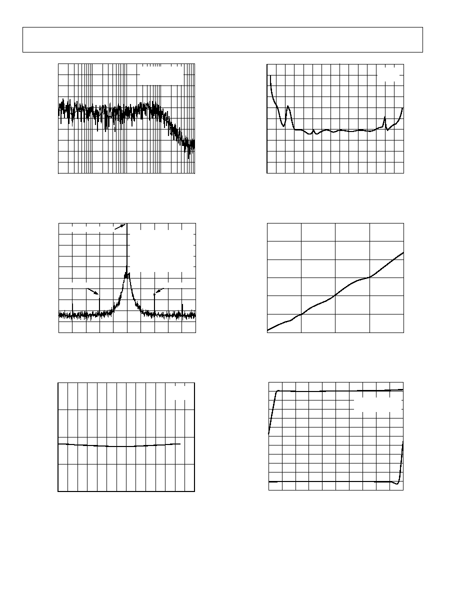
TYPICAL PERFORMANCE CHARACTERISTICS
Figure 5. Parameter Data for the RF Input
0
30
5
10
25
20
15
0
1
2
4
6
3
5
RF INPUT FREQUENCY GHz
RF
INPUT
POWER
d
B
m
7
V
DD
= 3V
V
P
= 3V
T
A
= +85
o
C
T
A
= 40
o
C
T
A
= +25
o
C
Figure 6. Input Sensitivity
0
60
2kHz
10
50
70
90
30
40
80
20
+2kHz
900MHz
1kHz
+1kHz
100
V
DD
= 3V, V
P
= 5V
I
CP
= 5mA
PFD FREQUENCY = 200kHz
LOOP BANDWIDTH = 20kHz
RES BANDWIDTH = 10Hz
VIDEO BANDWIDTH = 10Hz
SWEEP = 1.9 SECONDS
AVERAGES = 10
93.0dBc/Hz
FREQUENCY
OUTPUT POWER
dB
REF LEVEL = 14.3dBm
Figure 7. Phase Noise (900 MHz, 200 kHz, 20 kHz)
100Hz
1MHz
40
50
60
70
80
90
100
110
120
130
140
FREQUENCY OFFSET FROM 900MHz CARRIER
P
HAS
E
NOIS
E
dBc/Hz
10dB/DIV
R
L
= 40dBc/Hz
RMS NOISE = 0.36
o
Figure 8. Integrated Phase Noise (900 MHz, 200 kHz, 20 kHz)
0
60
10
50
70
90
30
40
80
20
100
OUTPUT POWER
dB
REF LEVEL = 14.0dBm
400kHz
+400kHz
900MHz
200kHz
+200kHz
FREQUENCY
V
DD
= 3V, V
P
= 5V
I
CP
= 5mA
PFD FREQUENCY = 200kHz
LOOP BANDWIDTH = 20kHz
RES BANDWIDTH = 1kHz
VIDEO BANDWIDTH = 1kHz
SWEEP = 2.5 SECONDS
AVERAGES = 30
91.0dBc/Hz
Figure 9. Reference Spurs (900 MHz, 200 kHz, 20 kHz)
0
60
10
50
70
90
30
40
80
20
100
OUTPUT POWER
dB
REF LEVEL = 10dBm
2kHz
+2kHz
6400MHz
1kHz
+1kHz
FREQUENCY
V
DD
= 3V, V
P
= 5V
I
CP
= 5mA
PFD FREQUENCY = 1MHz
LOOP BANDWIDTH = 100kHz
RES BANDWIDTH = 10Hz
VIDEO BANDWIDTH = 10Hz
SWEEP = 1.9 SECONDS
AVERAGES = 10
83.0dBc/Hz
Figure 10. Phase Noise (6.4 GHz, 1 MHz, 100 kHz)
Rev. 0 | Page 7 of 20
ADF4107
100Hz
1MHz
40
50
60
70
80
90
100
110
120
130
140
FREQUENCY OFFSET FROM 6400MHz CARRIER
P
HAS
E
NOIS
E
dBc/Hz
10dB/DIV
R
L
= 40dBc/Hz
RMS NOISE = 1.85
o
Figure 11. Integrated Phase Noise (6.4 GHz, 1 MHz, 100 kHz)
0
60
10
50
70
90
30
40
80
20
100
OUTP
UT P
O
W
E
R
dB
REF LEVEL = 10dBm
2MHz
+2MHz
6400MHz
1MHz
+1MHz
FREQUENCY
V
DD
= 3V, V
P
= 5V
I
CP
= 5mA
PFD FREQUENCY = 1MHz
LOOP BANDWIDTH = 100kHz
RES BANDWIDTH = 1kHz
VIDEO BANDWIDTH = 1kHz
SWEEP = 13 SECONDS
AVERAGES = 1
65.0dBc/Hz
66.0dBc/Hz
Figure 12. Reference Spurs (6.4 GHz, 1 MHz, 100 kHz)
60
70
100
40
100
20
0
20
40
60
80
80
90
V
DD
= 3V
V
P
= 3V
TEMPERATURE
o
C
P
HAS
E
NOIS
E
dBc/Hz
Figure 13. Phase Noise (6.4 GHz, 1 MHz, 100 kHz) vs. Temperature
5
15
45
0
1
2
3
4
25
35
TUNING VOLTAGE V
FIRS
T RE
FE
RE
NCE
S
P
U
R
dBc
5
55
85
65
75
105
95
V
DD
= 3V
V
P
= 5V
Figure 14. Reference Spurs vs. V
TUNE
(6.4 GHz, 1 MHz, 100 kHz)
120
130
180
10k
100M
100k
1M
10M
140
150
160
170
PHASE DETECTOR FREQUENCY Hz
P
HAS
E
NOIS
E
dBc/Hz
V
DD
= 3V
V
P
= 5V
Figure 15. Phase Noise (referred to CP output) vs. PFD Frequency
6
5
6
0
2.0
0.5
1.0
1.5
4
3
2
1
V
CP
V
I
CP
mA
0
1
2
3
4
5
4.0
2.5
3.0
3.5
5.0
4.5
V
P
= 5V
I
CP
SETTLING = 5mA
Figure 16. Charge Pump Output Characteristics
Rev. 0 | Page 8 of 20
ADF4107
Rev. 0 | Page 9 of 20
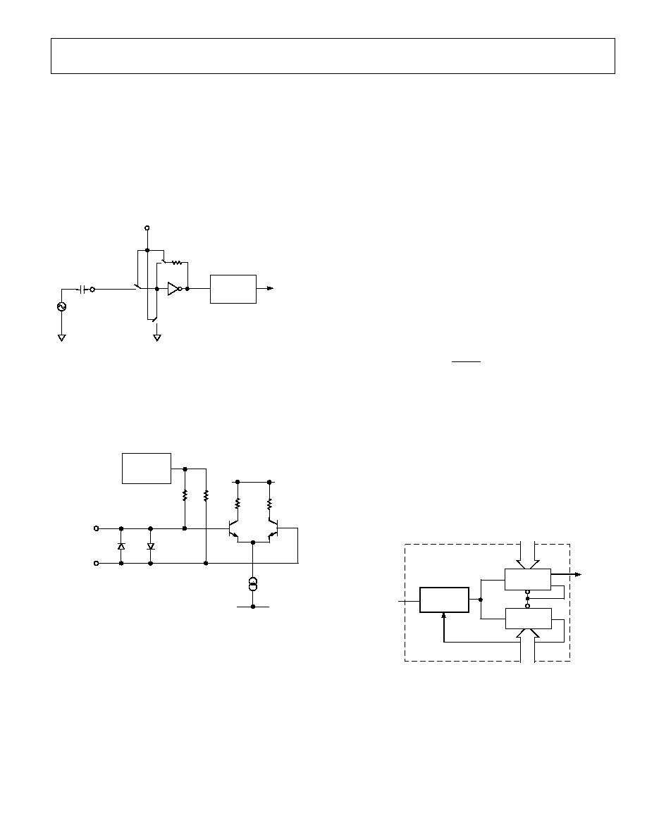
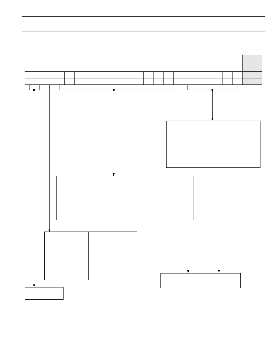
FUNCTIONAL DESCRIPTION
Reference Input Stage
The Reference Input stage is shown in Figure 17. SW1 and SW2
are normally closed switches. SW3 is normally open. When
power-down is initiated, SW3 is closed and SW1 and SW2 are
opened. This ensures that there is no loading of the REF
IN
pin
on power-down.
100k
NC
REF
IN
NC
NO
SW1
SW2
BUFFER
SW3
TO R COUNTER
POWER-DOWN
CONTROL
Figure 17. Reference Input Stage
RF Input Stage
The RF input stage is shown in Figure 18. It is followed by a
2-stage limiting amplifier to generate the CML clock levels
needed for the prescaler.
500
1.6V
500
AGND
BIAS
GENERATOR
RF
IN
A
RF
IN
B
AV
DD
Figure 18. RF Input Stage
Prescaler (P/P + 1)
The dual-modulus prescaler (P/P + 1), along with the A and B
counters, enables the large division ratio, N, to be realized
(N = BP + A). The dual-modulus prescaler, operating at CML
levels, takes the clock from the RF input stage and divides it
down to a manageable frequency for the CMOS A and B
counters. The prescaler is programmable. It can be set in
software to 8/9, 16/17, 32/33, or 64/65. It is based on a
synchronous 4/5 core. A minimum divide ratio is possible for
fully contiguous output frequencies. This minimum is
determined by P, the prescaler value, and is given by: (P
2
P).
A and B Counters
The A and B CMOS counters combine with the dual-modulus
prescaler to allow a wide ranging division ratio in the PLL
feedback counter. The counters are specified to work when the
prescaler output is 300 MHz or less. Thus, with an RF input
frequency of 4.0 GHz, a prescaler value of 16/17 is valid but a
value of 8/9 is not valid.
Pulse Swallow Function
The A and B counters, in conjunction with the dual-modulus
prescaler, make it possible to generate output frequencies that
are spaced only by the reference frequency divided by R. The
equation for the VCO frequency is as follows:
(
)
[
]
R
f
A
B
P
f
REFIN
VCO
×
+
×
=
f
VCO
Output frequency of external voltage controlled
oscillator (VCO).
P
Preset modulus of dual-modulus prescaler
(8/9, 16/17, etc.).
B
Preset divide ratio of binary 13-bit counter
(3 to 8191).
A
Preset divide ratio of binary 6-bit swallow counter
(0 to 63).
f
REFIN
External reference frequency oscillator.
LOAD
LOAD
FROM RF
INPUT STAGE
PRESCALER
P/P + 1
13-BIT B
COUNTER
TO PFD
6-BIT A
COUNTER
N DIVIDER
MODULUS
CONTROL
N = BP + A
Figure 19. A and B Counters
R Counter
The 14-bit R counter allows the input reference frequency to be
divided down to produce the reference clock to the phase
frequency detector (PFD). Division ratios from 1 to 16,383 are
allowed.
ADF4107
Phase Frequency Detector and Charge
Pump
The phase frequency detector (PFD) takes inputs from the R
counter and N counter (N = BP + A) and produces an output
proportional to the phase and frequency difference between
them. Figure 20 is a simplified schematic. The PFD includes a
programmable delay element that controls the width of the
antibacklash pulse. This pulse ensures that there is no dead zone
in the PFD transfer function and minimizes phase noise and
reference spurs. Two bits in the reference counter latch, ABP2
and ABP1, control the width of the pulse. See Figure 23.
HI
HI
D1
D2
Q1
Q2
CLR1
CLR2
CP
U1
U2
UP
DOWN
ABP2
ABP1
CPGND
U3
R DIVIDER
PROGRAMMABLE
DELAY
N DIVIDER
V
P
CHARGE
PUMP
Figure 20. PFD Simplified Schematic and Timing (in Lock)
MUXOUT and Lock Detect
The output multiplexer on the ADF4107 allows the user to
access various internal points on the chip. The state of
MUXOUT is controlled by M3, M2, and M1 in the function
latch. Figure 25 shows the full truth table. Figure 21 shows the
MUXOUT section in block diagram form.
Lock Detect
MUXOUT can be programmed for two types of lock detect:
digital lock detect and analog lock detect.
Digital lock detect is active high. When the lock detect precision
(LDP) bit in the R counter latch is set to 0, digital lock detect is
set high when the phase error on three consecutive phase
detector (PD) cycles is less than 15 ns. With LDP set to 1, five
consecutive cycles of less than 15 ns are required to set the lock
detect. It will stay set high until a phase error of greater than
25 ns is detected on any subsequent PD cycle.
The N-channel open-drain analog lock detect should be
operated with an external pull-up resistor of 10 k nominal.
When lock has been detected, this output will be high with
narrow, low-going pulses.
DGND
DV
DD
CONTROL
MUX
ANALOG LOCK DETECT
DIGITAL LOCK DETECT
R COUNTER OUTPUT
N COUNTER OUTPUT
SDOUT
MUXOUT
Figure 21. MUXOUT Circuit
Input Shift Register
The ADF4107 digital section includes a 24-bit input shift
register, a 14-bit R counter, and a 19-bit N counter, comprising a
6-bit A counter and a 13-bit B counter. Data is clocked into the
24-bit shift register on each rising edge of CLK. The data is
clocked in MSB first. Data is transferred from the shift register
to one of four latches on the rising edge of LE. The destination
latch is determined by the state of the two control bits (C2, C1)
in the shift register. These are the two LSBs, DB1 and DB0, as
shown in the timing diagram of Figure 2. The truth table for
these bits is shown in Table 5. Figure 22 shows a summary of
how the latches are programmed.
Table 5. C2, C1 Truth Table
Control Bits
C2 C1
Data Latch
0 0 R
Counter
0
1
N Counter (A and B)
1
0
Function Latch (Including Prescaler)
1 1 Initialization
Latch
Rev. 0 | Page 10 of 20
ADF4107
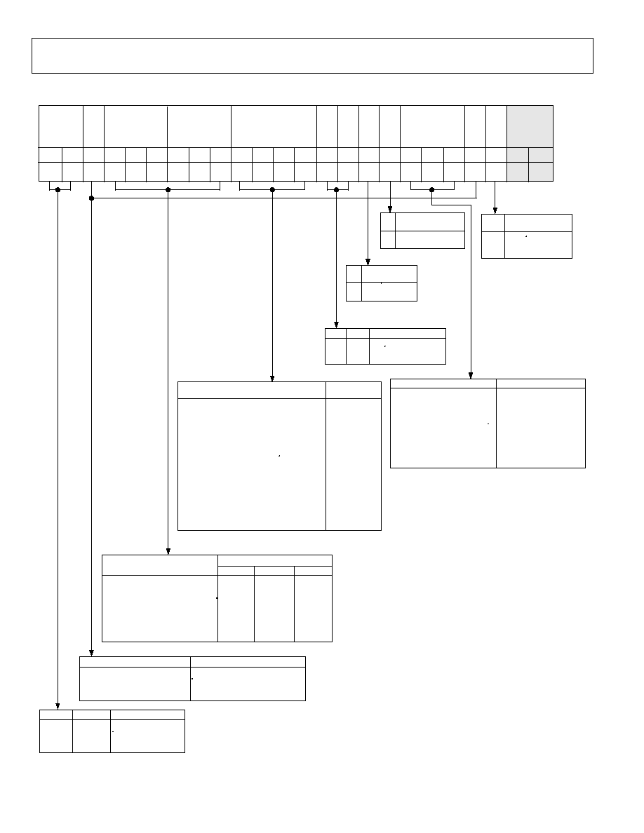
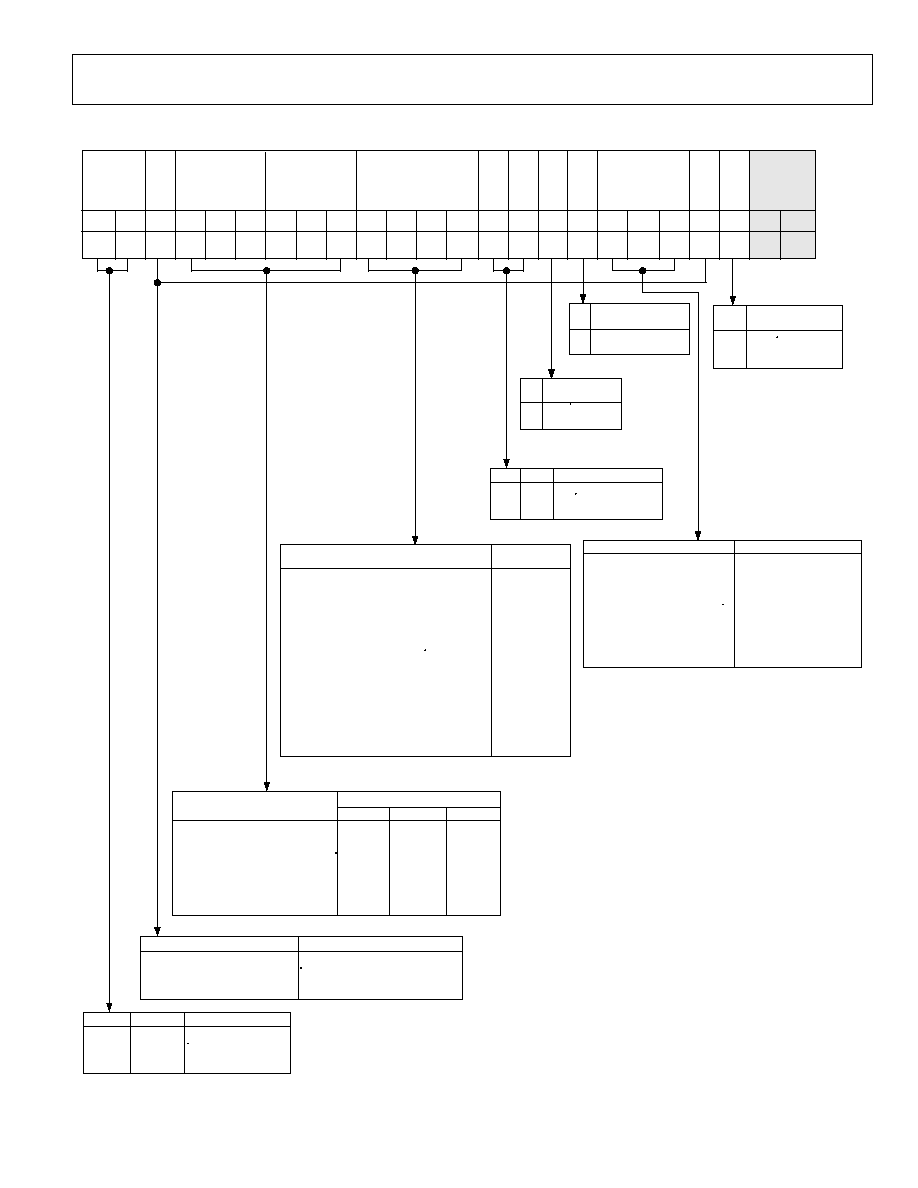
Latch Summary
DB20 DB19 DB18 DB17 DB16 DB15 DB14 DB13 DB12 DB11 DB10 DB9
DB8
DB7
DB6
DB5
DB4
DB3
DB2
DB1
DB0
C2 (0) C1 (0)
R1
R2
R3
R4
R5
R6
R7
R8
R9
R10
R11
R12
R13
R14
ABP1
ABP2
T1
T2
LDP
DB21
DB22
DB23
0
0
X
DB20 DB19 DB18 DB17 DB16 DB15 DB14 DB13 DB12 DB11 DB10 DB9
DB8
DB7
DB6
DB5
DB4
DB3
DB2
DB1
DB0
C2 (0) C1 (1)
A1
A2
A3
A4
A5
B1
B2
B3
B4
B5
B6
B7
B8
B9
B10
B11
B12
B13
A6
DB21
DB22
DB23
G1
X
X
DB20 DB19 DB18 DB17 DB16 DB15 DB14 DB13 DB12 DB11 DB10 DB9
DB8
DB7
DB6
DB5
DB4
DB3
DB2
DB1
DB0
C2 (1) C1 (0)
F1
PD1
M1
M2
M3
F3
P1
P2
CPI1
CPI2
CPI5
CPI6
TC4
PD2
F2
CPI3
CPI4
DB21
TC3
TC2
TC1
DB22
DB23
F4
F5
DB20 DB19 DB18 DB17 DB16 DB15 DB14 DB13 DB12 DB11 DB10 DB9
DB8
DB7
DB6
DB5
DB4
DB3
DB2
DB1
DB0
C2 (1) C1 (1)
F1
PD1
M1
M2
M3
F3
P1
P2
CPI1
CPI2
CPI5
CPI6
TC4
PD2
F2
CPI3
CPI4
DB21
TC3
TC2
TC1
DB22
DB23
F4
F5
REFERENCE COUNTER LATCH
RESERVED
LOCK
DE
TE
CT
PR
EC
ISION
TEST
MODE BITS
ANTI-
BACKLASH
WIDTH
14-BIT REFERENCE COUNTER
CONTROL
BITS
RESERVED
13-BIT B COUNTER
6-BIT A COUNTER
CONTROL
BITS
N COUNTER LATCH
CP GAIN
FUNCTION LATCH
PRESCALER
VALUE
POW
E
R
-
DOWN 2
CURRENT
SETTING
2
CURRENT
SETTING
1
TIMER COUNTER
CONTROL
FASTLOCK
MO
DE
FASTLOCK
E
NABLE
CP
THRE
E
-
STA
T
E
PD
P
O
LARITY
MUXOUT
CONTROL
POW
E
R
-
DOWN 1
COUNTE
R
R
ESET
CONTROL
BITS
PRESCALER
VALUE
POW
E
R
-
DOWN 2
CURRENT
SETTING
2
CURRENT
SETTING
1
TIMER COUNTER
CONTROL
FASTLOCK
MO
DE
FASTLOCK
E
NABLE
CP
T
HRE
E
-
STA
T
E
PD
P
O
LARITY
MUXOUT
CONTROL
POW
E
R
-
DOWN 1
COUNTE
R
R
ESET
CONTROL
BITS
INITIALIZATION LATCH
Figure 22. Latch Summary
Rev. 0 | Page 11 of 20
ADF4107
Rev. 0 | Page 12 of 20
Reference Counter Latch Map
LDP
0
1
ABP2
ABP1
0
0
2.9ns
0
1
1.3ns
1
0
6.0ns
1
1
2.9ns
R14
R13
R12
..........
R3
R2
R1
0
0
0
..........
0
0
1
1
0
0
0
..........
0
1
0
2
0
0
0
..........
0
1
1
3
0
0
0
..........
1
0
0
4
.
.
.
..........
.
.
.
.
.
.
.
..........
.
.
.
.
.
.
.
..........
.
.
.
.
1
1
1
..........
1
0
0
16380
1
1
1
..........
1
0
1
16381
1
1
1
..........
1
1
0
16382
1
1
1
..........
1
1
1
16383
X
= DON'T CARE
DB20 DB19 DB18 DB17 DB16 DB15 DB14 DB13 DB12 DB11 DB10 DB9
DB8
DB7
DB6
DB5
DB4
DB3
DB2
DB1
DB0
C2 (0) C1 (0)
R1
R2
R3
R4
R5
R6
R7
R8
R9
R10
R11
R12
R13
R14
ABP1
ABP2
T1
T2
LDP
DB21
DB22
DB23
0
0
X
RESERVED
LOCK
DE
TE
CT
PRECISION
TEST
MODE BITS
ANTI-
BACKLASH
WIDTH
14-BIT REFERENCE COUNTER
CONTROL
BITS
DIVIDE RATIO
ANTIBACKLASH PULSEWIDTH
TEST MODE BITS
SHOULD BE SET
TO 00 FOR NORMAL
OPERATION.
OPERATION
THREE CONSECUTIVE CYCLES OF PHASE DELAY LESS THAN
15ns MUST OCCUR BEFORE LOCK DETECT IS SET.
FIVE CONSECUTIVE CYCLES OF PHASE DELAY LESS THAN
15ns MUST OCCUR BEFORE LOCK DETECT IS SET.
BOTH OF THESE BITS
MUST BE SET TO 0 FOR
NORMAL OPERATION.
Figure 23. Reference Counter Latch Map
ADF4107
Rev. 0 | Page 13 of 20
AB Counter Latch Map
DB20
DB19
DB18
DB17
DB16
DB15
DB14
DB13
DB12
DB11 DB10
DB9
DB8
DB7
DB6
DB5
DB4
DB3
DB2
DB1
DB0
C2 (0) C1 (1)
A1
A2
A3
A4
A5
B1
B2
B3
B4
B5
B6
B7
B8
B9
B10
B11
B12
B13
A6
DB21
DB22
DB23
G1
0
0
0
1
1
0
F4 (FUNCTION LATCH)
FASTLOCK ENABLE
1
1
A6
A5
..........
A2
A1
0
0
..........
0
0
0
0
0
..........
0
1
1
0
0
..........
1
0
2
0
0
..........
1
1
3
.
.
..........
.
.
.
.
.
..........
.
.
.
.
.
..........
.
.
.
1
1
..........
0
0
60
1
1
..........
0
1
61
1
1
..........
1
0
62
1
1
..........
1
1
63
X
X
B13
B12
B11
B3
B2
B1
0
0
0
..........
0
0
0
0
0
0
..........
0
0
1
0
0
0
..........
0
1
0
0
0
0
..........
0
1
1
3
.
.
.
..........
.
.
.
.
.
.
.
..........
.
.
.
.
.
.
.
..........
.
.
.
.
1
1
1
..........
1
0
0
8188
1
1
1
..........
1
0
1
8189
1
1
1
..........
1
1
0
8190
1
1
1
..........
1
1
1
8191
X = DON'T CARE
RESERVED
13-BIT B COUNTER
6-BIT A COUNTER
CONTROL
BITS
CP G
A
IN
A COUNTER
DIVIDE RATIO
B COUNTER DIVIDE RATIO
NOT ALLOWED
NOT ALLOWED
NOT ALLOWED
THESE BITS ARE NOT USED
BY THE DEVICE AND ARE
DON'T CARE BITS.
OPERATION
CP GAIN
CHARGE PUMP CURRENT
SETTING 1 IS PERMANENTLY USED.
CHARGE PUMP CURRENT
SETTING 2 IS PERMANENTLY USED.
CHARGE PUMP CURRENT
SETTING 1 IS USED.
CHARGE PUMP CURRENT IS
SWITCHED TO SETTING 2. THE
TIME SPENT IN SETTING 2 IS
DEPENDENT ON WHICH FASTLOCK
MODE IS USED. SEE FUNCTION
LATCH DESCRIPTION.
N = BP + A, P IS PRESCALER VALUE SET IN THE FUNCTION
LATCH. B MUST BE GREATER THAN OR EQUAL TO A. FOR
CONTINUOUSLY ADJACENT VALUES OF (N
× F
REF
), AT THE
OUTPUT, N
MIN
IS (P
2
P).
Figure 24. AB Counter Latch Map
ADF4107
Rev. 0 | Page 14 of 20
Function Latch Map
P2
P1
0
0
8/9
0
1
16/17
1
0
32/33
1
1
64/65
PD2
PD1
MODE
0
X
X
1
X
0
1
0
1
1
1
1
CPI6
CPI5
CP14
CPI3
CPI2
CPI1
3k
5.1k
11k
0
0
0
1.06
0.625
0.289
0
0
1
2.12
1.25
0.580
0
1
0
3.18
1.875
0.870
0
1
1
4.24
2.5
1.160
1
0
0
5.30
3.125
1.450
1
0
1
6.36
3.75
1.730
1
1
0
7.42
4.375
2.020
1
1
1
8.50
5.0
2.320
TC4
TC3
TC2
TC1
0
0
0
0
3
0
0
0
1
7
0
0
1
0
11
0
0
1
1
15
0
1
0
0
19
0
1
0
1
23
0
1
1
0
27
0
1
1
1
31
1
0
0
0
35
1
0
0
1
39
1
0
1
0
43
1
0
1
1
47
1
1
0
0
51
1
1
0
1
55
1
1
1
0
59
1
1
1
1
63
F4
0
1
1
M3
M2
M1
0
0
0
0
0
1
0
1
0
0
1
1
1
0
0
1
0
1
1
1
0
1
1
1
F3
0
1
F2
0
1
F1
0
1
DB20 DB19 DB18 DB17 DB16 DB15 DB14 DB13 DB12 DB11 DB10 DB9
DB8
DB7
DB6
DB5
DB4
DB3
DB2
DB1
DB0
C2 (1) C1 (0)
F1
PD1
M1
M2
M3
F3
P1
P2
CPI1
CPI2
CPI5
CPI6
TC4
PD2
F2
CPI3
CPI4
DB21
TC3
TC2
TC1
DB22
DB23
F4
F5
THREE-STATE
F5
X
0
1
NEGATIVE
POSITIVE
PRESCALER
VALUE
POW
E
R
-
DOWN 2
CURRENT
SETTING
2
CURRENT
SETTING
1
TIMER COUNTER
CONTROL
FASTLOCK
MO
DE
FASTLOCK
E
NABLE
CP
THRE
E
-
STA
T
E
MUXOUT
CONTROL
POW
E
R
-
DOWN 1
COUNTE
R
R
ESET
CONTROL
BITS
PHASE DETECTOR
POLARITY
COUNTER
OPERATION
NORMAL
R, A, B COUNTERS
HELD IN RESET
CHARGE PUMP
OUTPUT
NORMAL
FASTLOCK DISABLED
FASTLOCK MODE 1
FASTLOCK MODE 2
FASTLOCK MODE
THREE-STATE OUTPUT
DIGITAL LOCK DETECT
(ACTIVE HIGH)
N DIVIDER OUTPUT
DV
DD
R DIVIDER OUTPUT
N-CHANNEL OPEN-DRAIN
LOCK DETECT
SERIAL DATA OUTPUT
DGND
OUTPUT
TIMEOUT
(PFD CYCLES)
I
CP
(mA)
ASYNCHRONOUS POWER-DOWN
NORMAL OPERATION
ASYNCHRONOUS POWER-DOWN
SYNCHRONOUS POWER-DOWN
CE PIN
PRESCALER VALUE
PD
P
O
LARITY
Figure 25. Function Latch Map
ADF4107
Rev. 0 | Page 15 of 20
Initialization Latch Map
P2
P1
0
0
8/9
0
1
16/17
1
0
32/33
1
1
64/65
PD2
PD1
MODE
0
X
X
1
X
0
1
0
1
1
1
1
CPI6
CPI5
CP14
CPI3
CPI2
CPI1
3k
5.1k
11k
0
0
0
1.06
0.625
0.289
0
0
1
2.12
1.25
0.580
0
1
0
3.18
1.875
0.870
0
1
1
4.24
2.5
1.160
1
0
0
5.30
3.125
1.450
1
0
1
6.36
3.75
1.730
1
1
0
7.42
4.375
2.020
1
1
1
8.50
5.0
2.320
TC4
TC3
TC2
TC1
0
0
0
0
3
0
0
0
1
7
0
0
1
0
11
0
0
1
1
15
0
1
0
0
19
0
1
0
1
23
0
1
1
0
27
0
1
1
1
31
1
0
0
0
35
1
0
0
1
39
1
0
1
0
43
1
0
1
1
47
1
1
0
0
51
1
1
0
1
55
1
1
1
0
59
1
1
1
1
63
F4
0
1
1
M3
M2
M1
0
0
0
0
0
1
0
1
0
0
1
1
1
0
0
1
0
1
1
1
0
1
1
1
F3
0
1
F2
0
1
F1
0
1
DB20 DB19 DB18 DB17 DB16 DB15 DB14 DB13 DB12 DB11 DB10 DB9
DB8
DB7
DB6
DB5
DB4
DB3
DB2
DB1
DB0
C2 (1) C1 (1)
F1
PD1
M1
M2
M3
F3
P1
P2
CPI1
CPI2
CPI5
CPI6
TC4
PD2
F2
CPI3
CPI4
DB21
TC3
TC2
TC1
DB22
DB23
F4
F5
THREE-STATE
F5
X
0
1
NEGATIVE
POSITIVE
PRESCALER
VALUE
POW
E
R
-
DOWN 2
CURRENT
SETTING
2
CURRENT
SETTING
1
TIMER COUNTER
CONTROL
FASTLOCK
MO
DE
FASTLOCK
E
NABLE
CP
THRE
E
-
STA
T
E
MUXOUT
CONTROL
POW
E
R
-
DOWN 1
COUNTE
R
R
ESET
CONTROL
BITS
PHASE DETECTOR
POLARITY
COUNTER
OPERATION
NORMAL
R, A, B COUNTERS
HELD IN RESET
CHARGE PUMP
OUTPUT
NORMAL
FASTLOCK DISABLED
FASTLOCK MODE 1
FASTLOCK MODE 2
FASTLOCK MODE
THREE-STATE OUTPUT
DIGITAL LOCK DETECT
(ACTIVE HIGH)
N DIVIDER OUTPUT
DV
DD
R DIVIDER OUTPUT
N-CHANNEL OPEN-DRAIN
LOCK DETECT
SERIAL DATA OUTPUT
DGND
OUTPUT
TIMEOUT
(PFD CYCLES)
I
CP
(mA)
ASYNCHRONOUS POWER-DOWN
NORMAL OPERATION
ASYNCHRONOUS POWER-DOWN
SYNCHRONOUS POWER-DOWN
CE PIN
PRESCALER VALUE
PD
P
O
LARITY
Figure 26. Initialization Latch Map

ADF4107
Rev. 0 | Page 16 of 20
i
i
Function Latch
The on-chip function latch is programmed with C2 and C1 set
to 1 and 0, respectively. Figure 25 shows the input data format
for programming the function latch.
Counter Reset
DB2 (F1) is the counter reset bit. When this bit is 1, the R
counter and the AB counters are reset. For normal operation,
this bit should be 0. Upon powering up, the F1 bit needs to be
disabled (set to 0). Then, the N counter resumes counting in
close alignment with the R counter. (The maximum error is one
prescaler cycle).
Power-Down
DB3 (PD1) and DB21 (PD2) provide programmable power-
down modes. They are enabled by the CE pin.
When the CE pin is low, the device is immediately disabled
regardless of the states of PD2 and PD1.
In the programmed asynchronous power-down, the device
powers down immediately after latching a 1 into the PD1 bit,
with the condition that PD2 has been loaded with a 0.
In the programmed synchronous power-down, the device
power-down is gated by the charge pump to prevent unwanted
frequency jumps. Once the power-down is enabled by writing
a 1 into PD1 (on condition that a 1 has also been loaded to
PD2), then the device will go into power-down on the
occurrence of the next charge pump event.
When a power-down is activated (either synchronous or
asynchronous mode, including CE pin activated power-down),
the following events occur:
·
All active dc current paths are removed.
·
The R, N, and timeout counters are forced to their load state
conditions.
·
The charge pump is forced into three-state mode.
·
The digital lock detect circuitry is reset.
·
The RF
IN
input is debiased.
·
The reference input buffer circuitry is disabled.
·
The input register remains active and capable of loading and
latching data.
MUXOUT Control
The on-chip multiplexer is controlled by M3, M2, M1 on the
ADF4107. Figure 25 shows the truth table.
Fastlock Enable B t
DB9 of the function latch is the fastlock enable bit. Fastlock is
enabled only when this bit is 1.
Fastlock Mode Bit
DB10 of the function latch is the fastlock mode bit. When
fastlock is enabled, this bit determines which fastlock mode is
used. If the fastlock mode bit is 0, then Fastlock Mode 1 is
selected; and if the fastlock mode bit is 1, then Fastlock Mode 2
is selected.
Fastlock Mode 1
The charge pump current is switched to the contents of Current
Setting 2.
The device enters fastlock by having a 1 written to the CP gain
bit in the AB counter latch. The device exits fastlock by having
a 0 written to the CP gain bit in the AB counter latch.
Fastlock Mode 2
The charge pump current is switched to the contents of Current
Setting 2.
The device enters fastlock by having a 1 written to the CP gain
bit in the AB counter latch. The device exits fastlock under the
control of the timer counter. After the timeout period
determined by the value in TC4TC1, the CP gain bit in the AB
counter latch is automatically reset to 0 and the device reverts to
normal mode instead of fastlock. See Figure 25 for the timeout
periods.
T mer Counter Control
The user has the option of programming two charge pump
currents. The intent is that Current Setting 1 is used when the
RF output is stable and the system is in a static state. Current
Setting 2 is meant to be used when the system is dynamic and in
a state of change (i.e., when a new output frequency is
programmed).
The normal sequence of events is as follows:
The user initially decides what the preferred charge pump
currents are going to be. For example, the choice may be 2.5 mA
as Current Setting 1 and 5 mA as Current Setting 2.
At the same time it must be decided how long the secondary
current is to stay active before reverting to the primary current.
This is controlled by the timer counter control bits, DB14DB11
(TC4TC1) in the function latch. The truth table is given in
Figure 25.
Now, to program a new output frequency, the user simply
programs the AB counter latch with new values for A and B. At
the same time, the CP gain bit can be set to 1, which sets the
charge pump with the value in CPI6CPI4 for a period of time
determined by TC4TC1. When this time is up, the charge
pump current reverts to the value set by CPI3CPI1. At the
same time the CP gain bit in the AB counter latch is reset to 0
and is now ready for the next time that the user wishes to
change the frequency.

ADF4107
Rev. 0 | Page 17 of 20
Note that there is an enable feature on the timer counter. It is
enabled when Fastlock Mode 2 is chosen by setting the fastlock
mode bit (DB10) in the function latch to 1.
Charge Pump Currents
CPI3, CPI2, and CPI1 program Current Setting 1 for the charge
pump. CPI6, CPI5, and CPI4 program Current Setting 2 for the
charge pump. The truth table is given in Figure 25.
Prescaler Value
P2 and P1 in the function latch set the prescaler values. The
prescaler value should be chosen so that the prescaler output
frequency is always less than or equal to 300 MHz. Thus, with
an RF frequency of 4 GHz, a prescaler value of 16/17 is valid but
a value of 8/9 is not valid.
PD Polarity
This bit sets the phase detector polarity bit. See Figure 25.
CP Three-State
This bit controls the CP output pin. With the bit set high, the CP
output is put into three-state. With the bit set low, the CP output
is enabled.
Initialization Latch
The initialization latch is programmed when C2 and C1 are set
to 1 and 1. This is essentially the same as the function latch
(programmed when C2, C1 = 1, 0).
However, when the initialization latch is programmed an
additional internal reset pulse is applied to the R and AB
counters. This pulse ensures that the AB counter is at load point
when the AB counter data is latched and the device will begin
counting in close phase alignment.
If the latch is programmed for synchronous power-down (CE
pin is high; PD1 bit is high; PD2 bit is low), the internal pulse
also triggers this power-down. The prescaler reference and the
oscillator input buffer are unaffected by the internal reset pulse
and so close phase alignment is maintained when counting
resumes.
When the first AB counter data is latched after initialization, the
internal reset pulse is again activated. However, successive AB
counter loads after this will not trigger the internal reset pulse.
Device Programming after Initial Power-Up
After initially powering up the device, there are three ways to
program the device.
Initialization Latch Method
Apply V
DD
.
Program the initialization latch (11 in two LSBs of input word).
Make sure that the F1 bit is programmed to 0.
Next, do a function latch load (10 in two LSBs of the control
word), making sure that the F1 bit is programmed to a 0.
Then do an R load (00 in two LSBs).
Then do an AB load (01 in two LSBs).
When the Initialization Latch is loaded, the following occurs:
1. The function latch contents are loaded.
2. An internal pulse resets the R, AB, and timeout counters to
load-state conditions and also three-states the charge
pump. Note that the prescaler band gap reference and the
oscillator input buffer are unaffected by the internal reset
pulse, allowing close phase alignment when counting
resumes.
3. Latching the first AB counter data after the initialization
word will activate the same internal reset pulse. Successive
AB loads will not trigger the internal reset pulse unless
there is another initialization.
CE Pin Method
Apply V
DD
.
Bring CE low to put the device into power-down. This is an
asychronous power-down in that it happens immediately.
Program the function latch (10).
Program the R counter latch (00).
Program the AB counter latch (01).
Bring CE high to take the device out of power-down. The R and
AB counters will now resume counting in close alignment.
Note that after CE goes high, a duration of 1 µs may be required
for the prescaler band gap voltage and oscillator input buffer
bias to reach steady state.
CE can be used to power the device up and down in order to
check for channel activity. The input register does not need to
be reprogrammed each time the device is disabled and enabled
as long as it has been programmed at least once after V
DD
was
initially applied.
Counter Reset Method
Apply V
DD
.
Do a Function Latch Load (10 in two LSBs). As part of this,
load 1 to the F1 bit. This enables the counter reset.
Do an R counter load (00 in two LSBs).
Do an AB counter load (01 in two LSBs).
Do a Function latch load (10 in two LSBs). As part of this,
load 0 to the F1 bit. This disables the counter reset.
This sequence provides the same close alignment as the
initialization method. It offers direct control over the internal
reset. Note that counter reset holds the counters at load point
and three-states the charge pump, but does not trigger
synchronous power-down.
ADF4107
Rev. 0 | Page 18 of 20
APPLICATIONS
Local Oscillator for LMDS Base Station
Transmitter
Figure 27 below shows the ADF4107 being used with a VCO to
produce the LO for an LMDS base station.
The reference input signal is applied to the circuit at FREF
IN
and, in this case, is terminated in 50 . A typical base station
system would have either a TCXO or an OCXO driving the
reference input without any 50 termination.
To have a channel spacing of 1 MHz at the output, the 10 MHz
reference input must be divided by 10, using the on-chip
reference divider of the ADF4107.
The charge pump output of the ADF4107 (Pin 2) drives the
loop filter. In calculating the loop filter component values, a
number of items need to be considered. In this example, the
loop filter was designed so that the overall phase margin for the
system would be 45°.
Other PLL system specifications are:
K
D
= 5.0 mA
K
V
= 80 MHz/V
Loop Bandwidth = 70 kHz
F
PFD
= 1 MHz
N = 6300
Extra Reference Spur Attenuation = 10 dB
All of these specifications are needed and used to derive the
loop filter component values shown in Figure 27.
Figure 27 gives a typical phase noise performance of
-83 dBc/Hz at 1 kHz offset from the carrier. Spurs are better
than -70 dBc.
The loop filter output drives the VCO, which, in turn, is fed
back to the RF input of the PLL synthesizer and also drives the
RF output terminal. A T-circuit configuration provides 50
matching between the VCO output, the RF output, and the RF
IN
terminal of the synthesizer.
In a PLL system, it is important to know when the system is in
lock. In Figure 27, this is accomplished by using the MUXOUT
signal from the synthesizer. The MUXOUT pin can be
programmed to monitor various internal signals in the
synthesizer. One of these is the LD or lock detect signal.
ADF4107
CE
CLK
DATA
LE
1000pF
1000pF
REFIN
100pF
CP
MUXOUT
CP
GND
AGND
DGND
100pF
820pF
47pF
100pF
51
1.7k
7.5k
100pF
18
NOTE
DECOUPLING CAPACITORS (0.1
µ
F/10pF) ON AV
DD
, DV
DD
,
V
P
OF THE ADF4107 AND ON V
CC
OF THE V956ME01 HAVE
BEEN OMITTED FROM THE DIAGRAM TO AID CLARITY.
S
P
I
COMP
AT
IBL
E
S
E
R
IAL
BUS
R
SET
RF
IN
A
RF
IN
B
AV
DD
DV
DD
V
P
FREF
IN
V
DD
V
P
LOCK
DETECT
V
CC
V956ME01
1, 3, 4, 5, 7, 8,
9, 11, 12, 13
18
18
100pF
RF
OUT
5.1k
7
15
16
8
2
14
6
5
1
9
4
3
14
2
10
51
Figure 27. 6.3 GHz Local Oscillator Using the ADF4107
ADF4107
Rev. 0 | Page 19 of 20
Interfacing
The ADF4107 has a simple SPITM compatible serial interface for
writing to the device. CLK, DATA, and LE control the data
transfer. When LE (Latch Enable) goes high, the 24 bits that
have been clocked into the input register on each rising edge of
CLK will get transferred to the appropriate latch. See Figure 2
for the timing diagram and Table 5 for the Latch truth table.
The maximum allowable serial clock rate is 20 MHz. This
means that the maximum update rate possible for the device is
833 kHz or one update every 1.2 µs. This is certainly more than
adequate for systems that have typical lock times in hundreds of
microseconds.
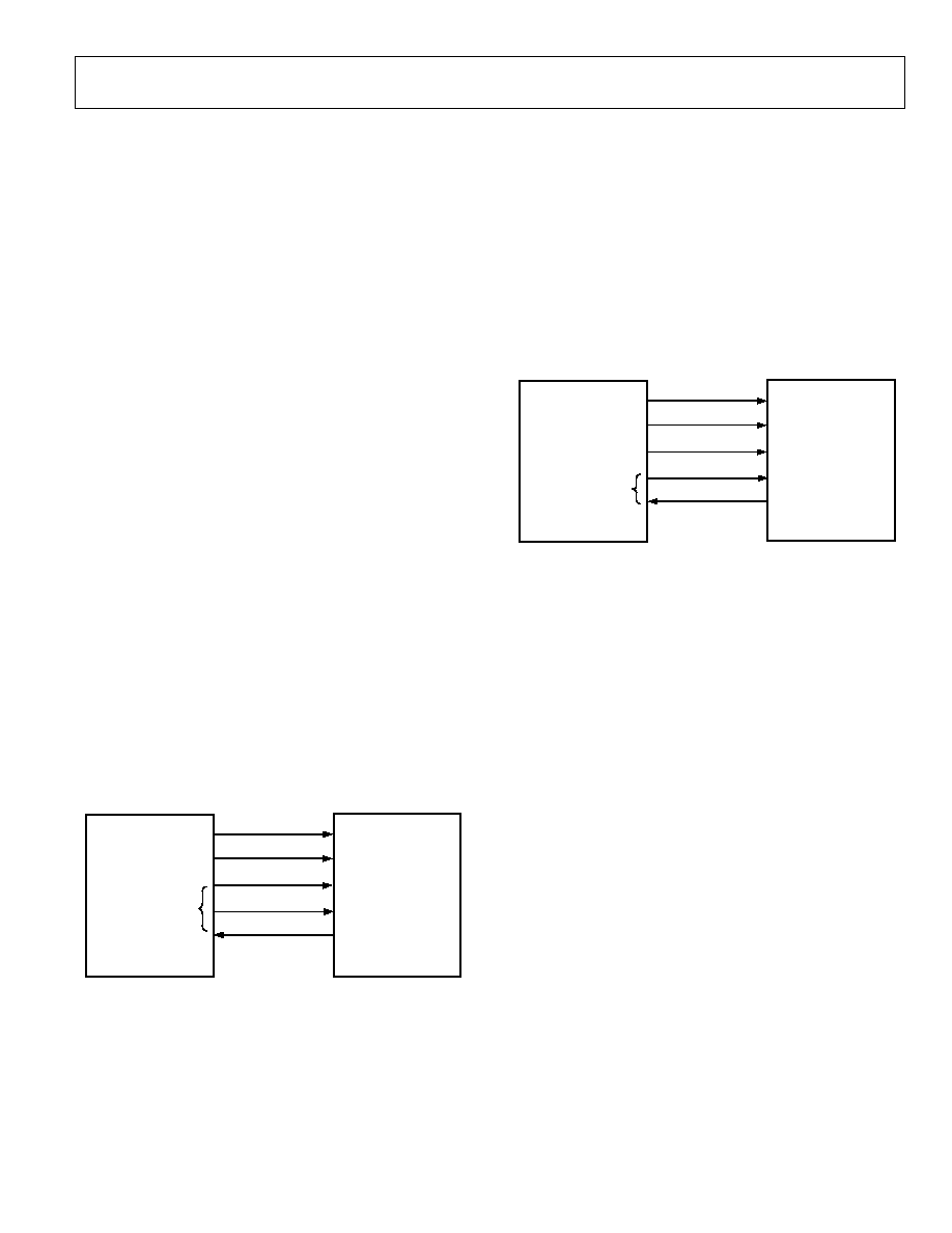
ADuC812 Interface
Figure 28 shows the interface between the ADF4107 and the
ADuC812 MicroConverter®. Since the ADuC812 is based on an
8051 core, this interface can be used with any 8051 based
microcontroller. The MicroConverter is set up for SPI master
mode with CPHA = 0. To initiate the operation, the I/O port
driving LE is brought low. Each latch of the ADF4107 needs a
24-bit word. This is accomplished by writing three 8-bit bytes
from the MicroConverter to the device. When the third byte has
been written, the LE input should be brought high to complete
the transfer.
On first applying power to the ADF4107, it needs four writes
(one each to the initialization latch, function latch, R counter
latch, and N counter latch) for the output to become active.
I/O port lines on the ADuC812 are also used to control power-
down (CE input) and to detect lock (MUXOUT configured as
lock detect and polled by the port input).
When operating in the mode described, the maximum
SCLOCK rate of the ADuC812 is 4 MHz. This means that the
maximum rate at which the output frequency can be changed
will be 166 kHz.
CLK
DATA
LE
CE
MUXOUT
(LOCK DETECT)
MOSI
ADF4107
SCLOCK
I/O PORTS
ADuC812
Figure 28. ADuC812 to ADF4107 Interface
ADSP2181 Interface
Figure 29 shows the interface between the ADF4107 and the
ADSP21xx Digital Signal Processor. The ADF4107 needs a
24-bit serial word for each latch write. The easiest way to
accomplish this using the ADSP21xx family is to use the
autobuffered transmit mode of operation with alternate
framing. This provides a means for transmitting an entire block
of serial data before an interrupt is generated. Set up the word
length for 8 bits and use three memory locations for each 24-bit
word. To program each 24-bit latch, store the three 8-bit bytes,
enable the autobuffered mode, and then write to the transmit
register of the DSP. This last operation initiates the autobuffer
transfer.
CLK
DATA
LE
CE
MUXOUT
(LOCK DETECT)
DT
ADF4107
SCLK
I/O FLAGS
ADSP21XX
TFS
Figure 29. ADSP-21xx to ADF4107 Interface
PCB Design Guidelines for Chip Scale
Package
The lands on the chip scale package (CP-20) are rectangular.
The printed circuit board pad for these should be 0.1 mm
longer than the package land length and 0.05 mm wider than
the package land width. The land should be centered on the pad.
This will ensure that the solder joint size is maximized. The
bottom of the chip scale package has a central thermal pad.
The thermal pad on the printed circuit board should be at least
as large as this exposed pad. On the printed circuit board, there
should be a clearance of at least 0.25 mm between the thermal
pad and the inner edges of the pad pattern. This will ensure that
shorting is avoided.
Thermal vias may be used on the printed circuit board thermal
pad to improve thermal performance of the package. If vias are
used, they should be incorporated in the thermal pad at 1.2 mm
pitch grid. The via diameter should be between 0.3 mm and
0.33 mm and the via barrel should be plated with 1 oz. copper
to plug the via.
The user should connect the printed circuit board thermal pad
to AGND.
ADF4107
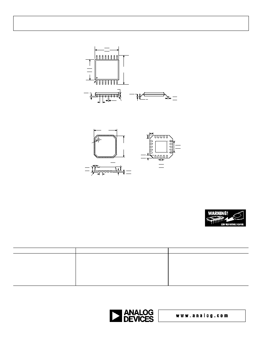
OUTLINE DIMENSIONS
1 6
9
8
1
PIN 1
SEATING
PLANE
8 °
0 °
4.50
4.40
4.30
6.40
BSC
5.10
5.00
4.90
0.65
BSC
0.15
0.05
1.20
MAX
0 .20
0 .09
0.75
0.60
0.45
0.30
0.19
COPLANARITY
0.10
COMPLIANT TO JEDEC STANDARDS MO-153AB
Figure 30. 16-Lead Thin Shrink Small Outline Package [TSSOP] (RU-16)--Dimensions shown in millimeters
1
20
5
6
11
16
15
BOTTOM
VIEW
10
2.25
2.10 SQ
1.95
0.75
0.55
0.35
0.30
0.23
0.18
0.50
BSC
12° MAX
0.20
REF
1.00 MAX
0.65 NOM
0.05
0.02
0.00
1.00
0.90
0.80
SEATING
PLANE
PIN 1
INDICATOR
TOP
VIEW
3.75
BSC SQ
4.0
BSC SQ
COPLANARITY
0.08
COMPLIANT TO JEDEC STANDARDS MO-220-VGGD-1
0.60
MAX
0.60
MAX
Figure 31. 20-Lead Frame Chip Scale Package [LFCSP] (CP-20)--Dimensions shown in millimeters
ESD CAUTION
ESD (electrostatic discharge) sensitive device. Electrostatic charges as high as 4000 V readily accumulate on the
human body and test equipment and can discharge without detection. Although this product features
proprietary ESD protection circuitry, permanent damage may occur on devices subjected to high energy
electrostatic discharges. Therefore, proper ESD precautions are recommended to avoid performance
degradation or loss of functionality.
ORDERING GUIDE
Model
Temperature Range
Package Option
ADF4107BRU
40°C to + 85°C
RU-16
ADF4107BRUREEL
40°C to + 85°C
RU-16
ADF4107BRUREEL7
40°C to + 85°C
RU-16
ADF4107BCP
40°C to + 85°C
CP-20
ADF4107BCPREEL
40°C to + 85°C
CP-20
ADF4107BCPREEL7
40°C to + 85°C
CP-20
RU = Thin Shrink Small Outline Package (TSSOP)
CP = Chip Scale Package
Contact the factory for chip availability.
Note that aluminum bond wire should not be used with the ADF4107 die.
© 2003 Analog Devices, Inc. All rights reserved. Trademarks and
registered trademarks are the property of their respective companies.
C03338-0-5/03(0)
Rev. 0 | Page 20 of 20
Document Outline