 | ÐлекÑÑоннÑй компоненÑ: ADF4002 | СкаÑаÑÑ:  PDF PDF  ZIP ZIP |
Äîêóìåíòàöèÿ è îïèñàíèÿ www.docs.chipfind.ru
Phase Detector/Frequency Synthesizer
ADF4002
Rev. 0
Information furnished by Analog Devices is believed to be accurate and reliable. However, no
responsibility is assumed by Analog Devices for its use, nor for any infringements of patents or other
rights of third parties that may result from its use. Specifications subject to change without notice. No
license is granted by implication or otherwise under any patent or patent rights of Analog Devices.
Trademarks and registered trademarks are the property of their respective owners.
One Technology Way, P.O. Box 9106, Norwood, MA 02062-9106, U.S.A.
Tel: 781.329.4700
www.analog.com
Fax: 781.461.3113
©2006 Analog Devices, Inc. All rights reserved.
FEATURES
400 MHz bandwidth
2.7 V to 3.3 V power supply
Separate charge pump supply (V
P
) allows extended
tuning voltage in 3 V systems
Programmable charge pump currents
3-wire serial interface
Analog and digital lock detect
Hardware and software power-down mode
200 MHz phase detector
APPLICATIONS
Clock conditioning
Clock generation
IF LO generation
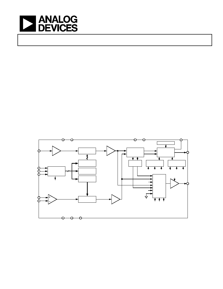
GENERAL DESCRIPTION
The ADF4002 frequency synthesizer is used to implement local
oscillators in the upconversion and downconversion sections of
wireless receivers and transmitters. It consists of a low-noise
digital phase frequency detector (PFD), a precision charge
pump, a programmable reference divider, and programmable
N divider. The 14-bit reference counter (R counter), allows
selectable REFIN frequencies at the PFD input. A complete
phase-locked loop (PLL) can be implemented if the synthesizer
is used with an external loop filter and voltage controlled
oscillator (VCO). In addition, by programming R and N to 1,
the part can be used as a stand alone PFD and charge pump.
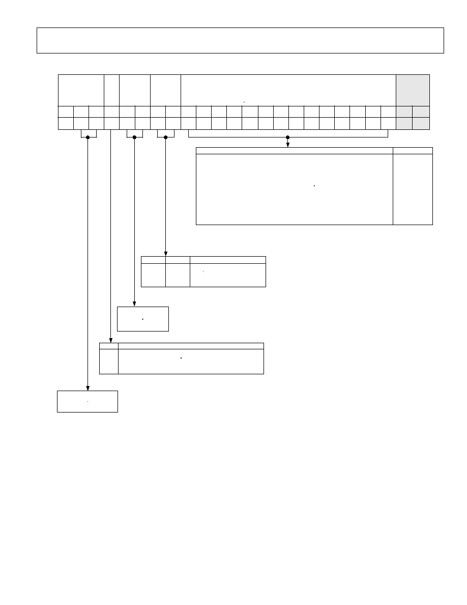
FUNCTIONAL BLOCK DIAGRAM
CLK
DATA
LE
REF
IN
RF
IN
A
RF
IN
B
24-BIT INPUT
REGISTER
SD
OUT
AV
DD
DV
DD
CE
AGND DGND
14-BIT
R COUNTER
R COUNTER
LATCH
22
14
FUNCTION
LATCH
N COUNTER
LATCH
13-BIT
N COUNTER
M3 M2 M1
MUX
SD
OUT
AV
DD
HIGH Z
MUXOUT
CPGND
R
SET
V
P
CP
PHASE
FREQUENCY
DETECTOR
LOCK
DETECT
REFERENCE
CHARGE
PUMP
CURRENT
SETTING 1
ADF4002
CPI3 CPI2 CPI1
CPI6 CPI5 CPI4
CURRENT
SETTING 2
06
05
2-
0
01
Figure 1.

ADF4002
Rev. 0 | Page 2 of 24
TABLE OF CONTENTS
Features .............................................................................................. 1
Applications....................................................................................... 1
General Description ......................................................................... 1
Functional Block Diagram .............................................................. 1
Revision History ............................................................................... 2
Specifications..................................................................................... 3
Timing Characteristics ................................................................ 4
Absolute Maximum Ratings............................................................ 5
Thermal Characteristics .............................................................. 5
ESD Caution.................................................................................. 5
Pin Configurations and Function Descriptions ........................... 6
Typical Performance Characteristics ............................................. 7
Theory of Operation ........................................................................ 8
Reference Input Section............................................................... 8
RF Input Stage............................................................................... 8
N Counter...................................................................................... 8
R Counter ...................................................................................... 8
Phase Frequency Detector (PFD) and Charge Pump.............. 8
MUXOUT and Lock Detect.........................................................9
Input Shift Register .......................................................................9
Latch Maps and Descriptions ....................................................... 10
Latch Summary........................................................................... 10
Reference Counter Latch Map.................................................. 11
N Counter Latch Map................................................................ 12
Function Latch Map................................................................... 13
Initialization Latch Map ............................................................ 14
The Function Latch.................................................................... 15
The Initialization Latch ............................................................. 16
Applications..................................................................................... 17
Very Low Jitter Encode Clock for High Speed Converters... 17
PFD............................................................................................... 18
Interfacing ................................................................................... 18
PCB Design Guidelines for Chip Scale Package .................... 18
Outline Dimensions ....................................................................... 20
Ordering Guide .......................................................................... 21
REVISION HISTORY
4/06--Revision 0: Initial Version

ADF4002
Rev. 0 | Page 3 of 24
SPECIFICATIONS
AV
DD
= DV
DD
= 3 V ± 10%, AV
DD
V
P
5.5 V, AGND = DGND = CPGND = 0 V, R
SET
= 5.1 k, dBm referred to 50 ,
T
A
= T
MAX
to T
MIN
, unless otherwise noted.
Table 1.
B
Version
1
Parameter Min
Typ
Max
Unit
Test
Conditions/Comments
RF CHARACTERISTICS
See Figure 12 for input circuit
RF Input Sensitivity
-10
0
dBm
RF Input Frequency (RF
IN
)
5
400
MHz
For RF
IN
< 5 MHz, ensure slew rate (SR) > 4 V/s
REFIN CHARACTERISTICS
REFIN Input Frequency
20
300
MHz
For REFIN < 20 MHz, ensure SR > 50 V/s
REFIN Input Sensitivity
2
0.8 V
DD
V p-p
Biased at AV
DD
/2
3
REFIN Input Capacitance
10
pF
REFIN Input Current
±100
A
PHASE DETECTOR
Phase Detector Frequency
4
200
MHz
CHARGE PUMP
Programmable, see Figure 19
I
CP
Sink/Source
High Value
5
mA
With R
SET
= 5.1 k
Low Value
625
A
Absolute Accuracy
2.5
%
With R
SET
= 5.1 k
R
SET
Range
3.0
11
k
See Figure 19
I
CP
Three-State Leakage
1
nA
T
A
= 25°C
I
CP
vs. V
CP
1.5
%
0.5 V V
CP
V
P
0.5 V
Sink and Source Current Matching
2
%
0.5 V V
CP
V
P
0.5 V
I
CP
vs. Temperature
2
%
V
CP
= V
P
/2
LOGIC INPUTS
V
IH
, Input High Voltage
1.4
V
V
IL
, Input Low Voltage
0.6
V
I
INH
, I
INL
, Input Current
±1
A
C
IN
, Input Capacitance
10
pF
LOGIC OUTPUTS
V
OH
, Output High Voltage
1.4
V
Open-drain output chosen, 1 k pull-up resistor to 1.8 V
V
OH
, Output High Voltage
V
DD
0.4
V
CMOS output chosen
I
OH
100
A
V
OL
, Output Low Voltage
0.4
V
I
OL
= 500 A
POWER SUPPLIES
AV
DD
2.7 3.3
V
DV
DD
AV
DD
V
P
AV
DD
5.5
V AV
DD
V
P
5.5 V
I
DD
5
(AI
DD
DD
+ DI )
5.0
6.0
mA
I
P
0.4
mA
T
A
= 25°C
Power-Down Mode
1
A
AI
DD
+ DI
DD
NOISE CHARACTERISTICS
Normalized Phase Noise Floor
6
222
dBc/Hz
1
Operating temperature range (B version) is 40°C to +85°C.
2
AV
DD
= DV
DD
= 3 V.
3
AC coupling ensures AV
DD
/2 bias.
4
Guaranteed by design. Sample tested to ensure compliance. Use of the PFD at frequencies above 104 MHz requires the minimum antibacklash pulse width enabled.
5
T
A
= 25°C; AV
DD
= DV
DD
= 3 V; RF
IN
= 350 MHz. The current for any other setup (25°C, 3.0 V) in mA is given by 2.35 + 0.0046 (REFIN) + 0.0062 (RF), RF frequency and REFIN
frequency in MHz.
6
The normalized phase noise floor is estimated by measuring the in-band phase noise at the output of the VCO and subtracting 20logN (where N is the N divider value)
and 10logF
PFD
. PN
SYNTH
= PN
TOT
10logF
PFD
20logN. All phase noise measurements were performed with an Agilent E5500 phase noise test system, using the EVAL-
ADF4002EB1 and the HP8644B as the PLL reference.
ADF4002
Rev. 0 | Page 4 of 24
TIMING CHARACTERISTICS
AV
DD
= DV
DD
= 3 V ± 10%, AV
DD
V
P
5.5 V, AGND = DGND = CPGND = 0 V, R
SET
= 5.1 k, dBm referred to 50 , T
A
= T
MAX
to T
MIN
,
unless otherwise noted.
1
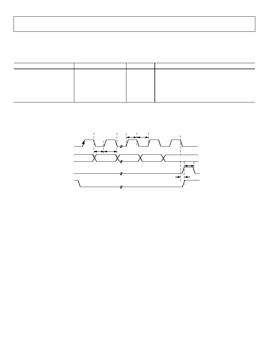
Table 2.
Parameter Limit
(B
Version)
2
Unit Test
Conditions/Comments
t
1
10
ns min
DATA to CLK setup time
t
2
10
ns min
DATA to CLK hold time
t
3
25
ns min
CLK high duration
t
4
25
ns min
CLK low duration
t
5
10
ns min
CLK to LE setup time
t
6
20
ns min
LE pulse width
1
Guaranteed by design, but not production tested.
2
Operating temperature range (B version) is 40°C to +85°C.
Timing Diagram
CLK
DB22
DB2
DATA
LE
t
1
LE
DB23 (MSB)
t
2
DB1 (CONTROL
BIT C2)
DB0 (LSB)
(CONTROL BIT C1)
t
3
t
4
t
6
t
5
06
05
2-
0
22
Figure 2. Timing Diagram
ADF4002
Rev. 0 | Page 5 of 24
ABSOLUTE MAXIMUM RATINGS
T
A
= 25°C, unless otherwise noted.
Table 3.
Parameter Rating
AV
DD
to GND
1
0.3 V to +3.6 V
AV
DD
to DV
DD
0.3 V to +0.3 V
V
P
to GND
0.3 V to +5.8 V
V
P
to AV
DD
0.3 V to +5.8 V
Digital I/O Voltage to GND
0.3 V to VDD + 0.3 V
Analog I/O Voltage to GND
0.3 V to V
P
+ 0.3 V
REFIN, RF
IN
A, RF
IN
B to GND
0.3 V to VDD + 0.3 V
Operating Temperature Range
Industrial (B Version)
40°C to +85°C
Storage Temperature Range
65°C to +125°C
Maximum Junction Temperature
150°C
Lead Temperature, Soldering
Vapor Phase (60 sec)
215°C
Infrared (15 sec)
220°C
Transistor Count
CMOS 6425
Bipolar 303
1
GND = AGND = DGND = 0 V.
Stresses above those listed under Absolute Maximum Ratings
may cause permanent damage to the device. This is a stress
rating only; functional operation of the device at these or any
other conditions above those indicated in the operational
section of this specification is not implied. Exposure to absolute
maximum rating conditions for extended periods may affect
device reliability.
This device is a high performance RF integrated circuit with an
ESD rating of <2 kV, and it is ESD sensitive. Proper precautions
should be taken for handling and assembly.
THERMAL CHARACTERISTICS
Table 4. Thermal Impedance
Package Type
JA
Unit
TSSOP 150.4
°C/W
LFCSP_VQ 122
°C/W
ESD CAUTION
ESD (electrostatic discharge) sensitive device. Electrostatic charges as high as 4000 V readily accumulate on
the human body and test equipment and can discharge without detection. Although this product features
proprietary ESD protection circuitry, permanent damage may occur on devices subjected to high energy
electrostatic discharges. Therefore, proper ESD precautions are recommended to avoid performance
degradation or loss of functionality.
ADF4002
Rev. 0 | Page 6 of 24
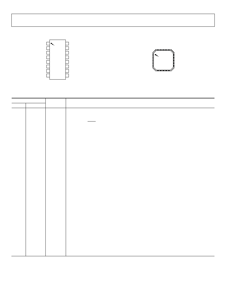
PIN CONFIGURATIONS AND FUNCTION DESCRIPTIONS
R
SET
CP
CPGND
AGND
MUXOUT
LE
DATA
CLK
CE
DGND
16
15
14
13
12
11
10
9
1
2
3
4
5
6
7
8
RF
IN
B
RF
IN
A
AV
DD
REF
IN
V
P
DV
DD
ADF4002
TOP VIEW
(Not to Scale)
06
052
-
00
2
PIN 1
INDICATOR
Figure 3. TSSOP (Top View)
15 MUXOUT
14 LE
13 DATA
12 CLK
CPGND 1
AGND 2
AGND 3
20
C
P
11 CE
6
7
8
DG
ND 9
DG
ND 10
4
5
19
18
17
16
RF
IN
B
RF
IN
A
R
SE
T
V
P
DV
DD
DV
DD
AV
DD
AV
DD
RE
F
IN
PIN 1
INDICATOR
ADF4002
TOP VIEW
(Not to Scale)
0
60
52
-
0
03
Figure 4. LFCSP_VQ (Top View)
Table 5. Pin Function Descriptions
Pin No.
TSSOP LFCSP_VQ Mnemonic
Description
1 19
R
SET
Connecting a resistor between this pin and CPGND sets the maximum charge pump output current.
The nominal voltage potential at the R
SET
pin is 0.66 V. The relationship between I
CP
and R
SET
is
SET
MAX
CP
R
I
5
.
25
=
Where R
SET
= 5.1 k and I
CP MAX
= 5 mA.
2 20
CP
Charge Pump Output. When enabled, this provides ±I
CP
to the external loop filter that, in turn, drives
the external VCO.
3
1
CPGND
Charge Pump Ground. This is the ground return path for the charge pump.
4
2, 3
AGND
Analog Ground. This is the ground return path of the RF input.
5 4
RF
IN
B
Complementary Input to the RF Input. This point must be decoupled to the ground plane with a small
bypass capacitor, typically 100 pF. See Figure 12.
6 5
RF
IN
A
Input to the RF Input. This small signal input is ac-coupled to the external VCO.
7 6,
7 AV
DD
Analog Power Supply. This can range from 2.7 V to 3.3 V. Decoupling capacitors to the analog ground
plane should be placed as close as possible to the AV
DD
pin. AV
DD
must be the same value as DV
DD
.
8 8
REF
IN
Reference Input. This is a CMOS input with a nominal threshold of V
DD
/2 and a dc equivalent input
resistance of 100 k. See Figure 11. This input can be driven from a TTL or CMOS crystal oscillator or it
can be ac-coupled.
9
9, 10
DGND
Digital Ground.
10 11
CE
Chip Enable. A logic low on this pin powers down the device and puts the charge pump output into
three-state mode. Taking this pin high powers up the device, depending on the status of the Power-
Down Bit F2.
11 12
CLK
Serial Clock Input. This serial clock is used to clock in the serial data to the registers. The data is
latched into the 24-bit shift register on the CLK rising edge. This input is a high impedance CMOS
input.
12 13
DATA Serial Data Input. The serial data is loaded MSB-first with the two LSBs being the control bits. This
input is a high impedance CMOS input.
13 14
LE
Load Enable, CMOS Input. When LE goes high, the data stored in the shift registers is loaded into one
of the four latches; the latch is selected using the control bits.
14 15
MUXOUT
This multiplexer output allows either the lock detect, the scaled RF, or the scaled reference frequency
to be accessed externally.
15 16,
17 DV
DD
Digital Power Supply. This can range from 2.7 V to 3.3 V. Decoupling capacitors to the digital ground
plane should be placed as close as possible to this pin. DV
DD
must be the same value as AV
DD
.
16 18
V
P
Charge Pump Power Supply. This should be greater than or equal to V
DD
. In systems where V
DD
is 3 V, it
can be set to 5.5 V and used to drive a VCO with a tuning range of up to 5 V.
ADF4002
Rev. 0 | Page 7 of 24
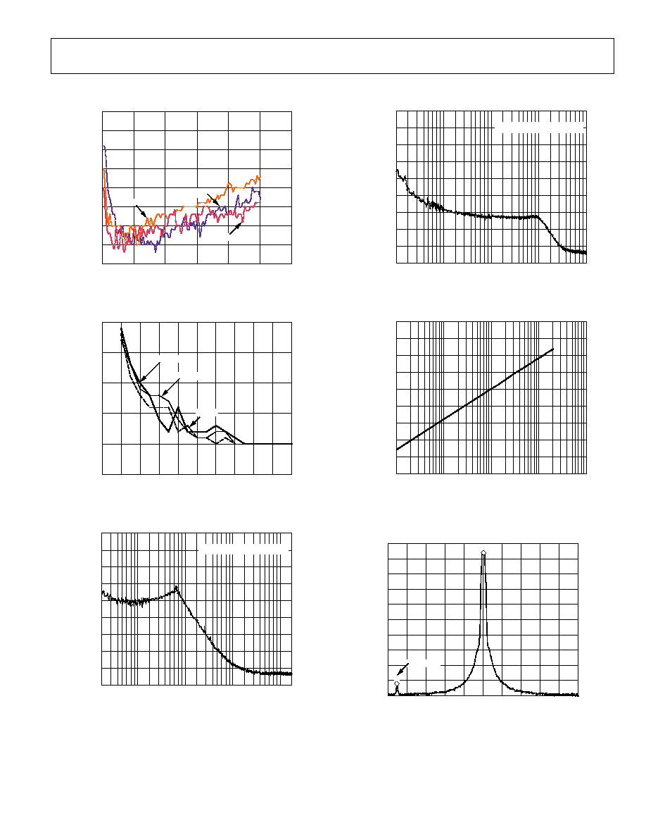
TYPICAL PERFORMANCE CHARACTERISTICS
0
5
10
15
20
25
30
40
35
0
100
200
300
400
500
600
06
05
2-
02
7
PO
W
E
R
(d
B
m
)
FREQUENCY (MHz)
40°C
+85°C
+25°C
Figure 5. RF Input Sensitivity
0
1
2
3
4
5
10
9
6
8
7
06
05
2-
0
26
P
O
W
E
R (
d
Bm
)
FREQUENCY (MHz)
0
5
10
15
20
25
40°C
+25°C
+85°C
Figure 6. RF Input Sensitivity, Low Frequency
70
80
90
100
110
120
130
140
150
160
1k
10k
100k
1M
10M
06
05
2-
0
31
P
HAS
E
N
O
I
S
E
(
d
Bc/
H
z
)
FREQUENCY OFFSET (Hz)
rms NOISE = 0.07 DEGREES
Figure 7. Integrated Phase Noise (400 MHz, 1 MHz, 50 kHz)
70
80
90
100
110
120
130
140
150
160
1k
10k
100k
1M
10M
06
05
2-
03
2
PO
W
E
R
(
d
B
c
/
H
z)
FREQUENCY OFFSET (Hz)
rms NOISE = 0.03 DEGREES
Figure 8. Integrated Phase Noise (400 MHz, PFD = 200 MHz, 50 kHz)
130
135
140
145
155
160
165
170
175
180
100k
1M
10M
100M
1G
06
05
2-
03
3
P
HAS
E
NO
I
S
E
(
d
Bc/
H
z
)
PFD FREQUENCY (Hz)
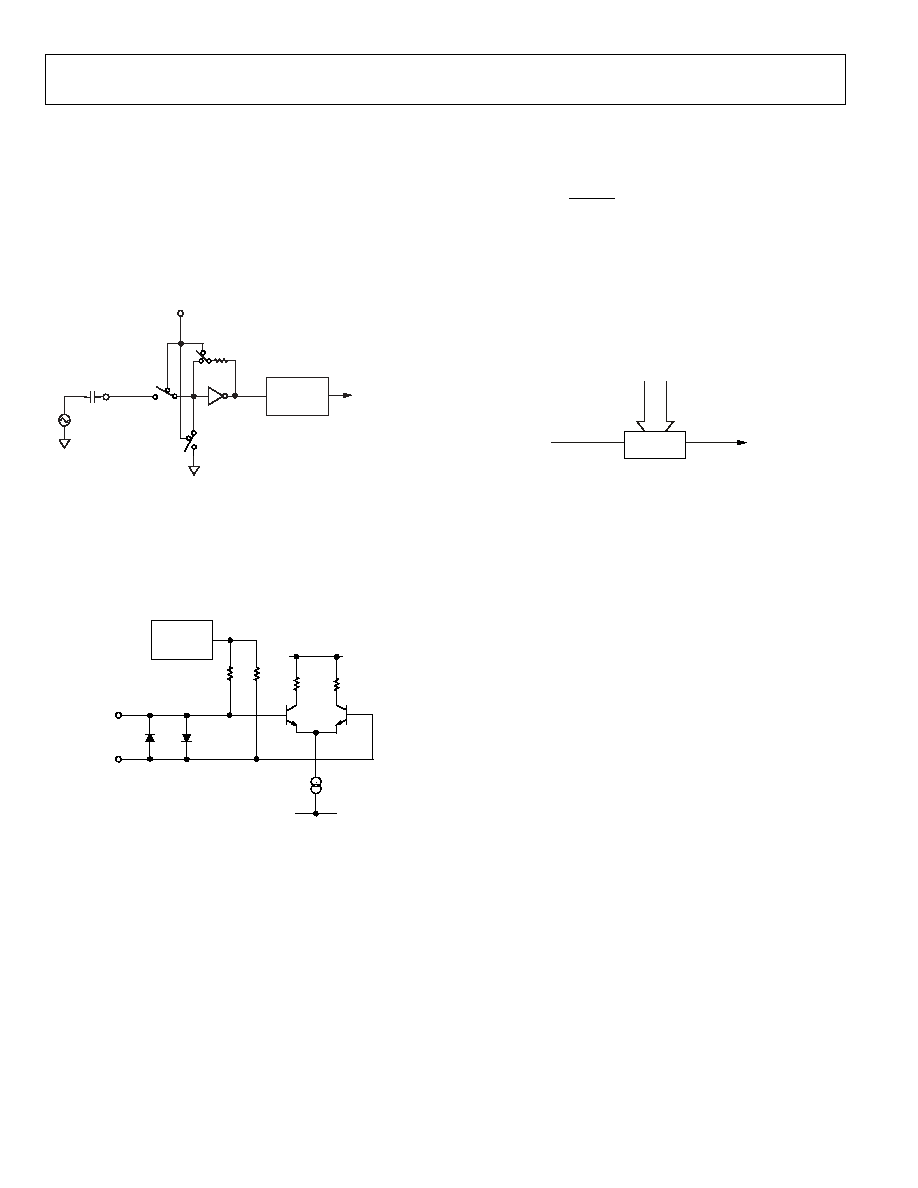
Figure 9. Phase Noise (Referred to CP Output) vs. PFD Frequency
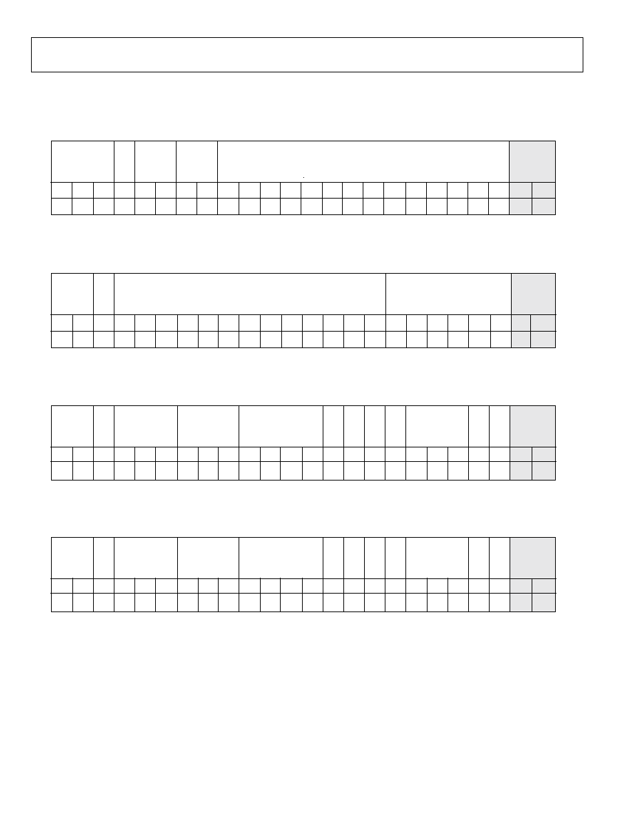
06
05
2-
0
30
REF 4dBm
SAMP LOG 10dB/
ATTN 10dB
VBW 20KHz
MKR1 1.000 MHz
94.5dBc
CENTER 399.995MHz
RES BW 20KHz
SPAN 2.2MHz
SWEEP 21ms (601pts)
94.5dBc
0
10
20
30
40
50
60
70
90
100
80
1
1R
Figure 10. Reference Spurs (400 MHz, 1 MHz, 7 kHz)
ADF4002
Rev. 0 | Page 8 of 24
THEORY OF OPERATION
REFERENCE INPUT SECTION
The reference input stage is shown in Figure 11. SW1 and SW2
are normally closed switches. SW3 is normally open. When
power-down is initiated, SW3 is closed and SW1 and SW2 are
opened. This ensures that there is no loading of the REF
IN
pin
on power-down.
100k
NC
REF
IN
NC
NO
SW1
SW2
BUFFER
SW3
TO R COUNTER
POWER-DOWN
CONTROL
0
605
2-
0
13
Figure 11. Reference Input Stage
RF INPUT STAGE
The RF input stage is shown in Figure 12. It is followed by a
2-stage limiting amplifier to generate the CML clock levels
needed for the N counter.
500
1.6V
500
AGND
BIAS
GENERATOR
RF
IN
A
RF
IN
B
AV
DD
06
05
2-
0
14
Figure 12. RF Input Stage
N COUNTER
The N CMOS counter allows a wide ranging division ratio in
the PLL feedback counter. Division ratios from 1 to 8191 are
allowed.
N and R Relationship
The N counter makes it possible to generate output frequencies
that are spaced only by the reference frequency divided by R.
The equation for the VCO frequency is
R
REFIN
f
N
VCO
f
×
=
where:
f
VCO
is the output frequency of external voltage controlled
oscillator (VCO).
N is the preset divide ratio of binary 13-bit counter (1 to 8191).
f
REFIN
is the external reference frequency oscillator.
TO PFD
FROM RF
INPUT STAGE
FROM N
COUNTER LATCH
13-BIT N
COUNTER
06
05
2-
02
1
Figure 13. N Counter
R COUNTER
The 14-bit R counter allows the input reference frequency to be
divided down to produce the reference clock to the phase
frequency detector (PFD). Division ratios from 1 to 16,383 are
allowed.
PHASE FREQUENCY DETECTOR (PFD) AND
CHARGE PUMP
The PFD takes inputs from the R counter and N counter and
produces an output proportional to the phase and frequency
difference between them. Figure 14 is a simplified schematic.
The PFD includes a programmable delay element that controls
the width of the antibacklash pulse. This pulse ensures that
there is no dead zone in the PFD transfer function, and
minimizes phase noise and reference spurs. Two bits in the
reference counter latch (ABP2 and ABP1) control the width of
the pulse. See Figure 17 for details. The smallest antibacklash
pulse width (1.3 ns) should be used if the desired PFD exceeds
104 MHz.
ADF4002
Rev. 0 | Page 9 of 24
HI
HI
D1
D2
Q1
Q2
CLR1
CLR2
CP
U1
U2
UP
DOWN
ABP2
ABP1
CPGND
U3
R DIVIDER
PROGRAMMABLE
DELAY
N DIVIDER
V
P
CHARGE
PUMP
06
05
2-
02
3
Figure 14. PFD Simplified Schematic and Timing (In Lock)
MUXOUT AND LOCK DETECT
The output multiplexer on the ADF4002 allows the user to
access various internal points on the chip. The state of
MUXOUT is controlled by M3, M2, and M1 in the function
latch. Figure 19 shows the full truth table. Figure 15 shows the
MUXOUT section in block diagram form.
DGND
DV
DD
CONTROL
MUX
ANALOG LOCK DETECT
DIGITAL LOCK DETECT
R COUNTER OUTPUT
N COUNTER OUTPUT
SDOUT
MUXOUT
0
605
2-
0
24
Figure 15. MUXOUT Circuit
Lock Detect
MUXOUT can be programmed for two types of lock detect:
digital lock detect and analog lock detect.
Digital lock detect is active high. When LDP in the R counter
latch is set to 0, digital lock detect is set high when the phase
error on three consecutive phase detector (PD) cycles is less
than 15 ns. With LDP set to 1, five consecutive cycles of less
than 15 ns are required to set the lock detect. It stays set at high
until a phase error of greater than 25 ns is detected on any
subsequent PD cycle. For PFD frequencies greater than 10 MHz,
analog lock detect is more accurate because of the smaller pulse
widths.
The N-channel, open-drain, analog lock detect should be
operated with an external pull-up resistor of 10 k nominal.
When lock has been detected this output is high with narrow,
low-going pulses.
INPUT SHIFT REGISTER
The ADF4002 digital section includes a 24-bit input shift
register, a 14-bit R counter, and a 13-bit N counter. Data is
clocked into the 24-bit shift register on each rising edge of CLK.
The data is clocked in MSB-first. Data is transferred from the
shift register to one of four latches on the rising edge of LE. The
destination latch is determined by the state of the two control
bits (C2, C1) in the shift register. These are the two LSBs, DB1
and DB0, as shown in the timing diagram (see Figure 2). Table 6
provides the truth table for these bits. Figure 16 shows a
summary of how the latches are programmed.
Table 6. C2, C1 Truth Table
Control Bits
C2 C1 Data Latch
0 0 R
Counter
0 1 N
Counter
1 0 Function
Latch
1 1 Initialization
Latch
ADF4002
Rev. 0 | Page 10 of 24
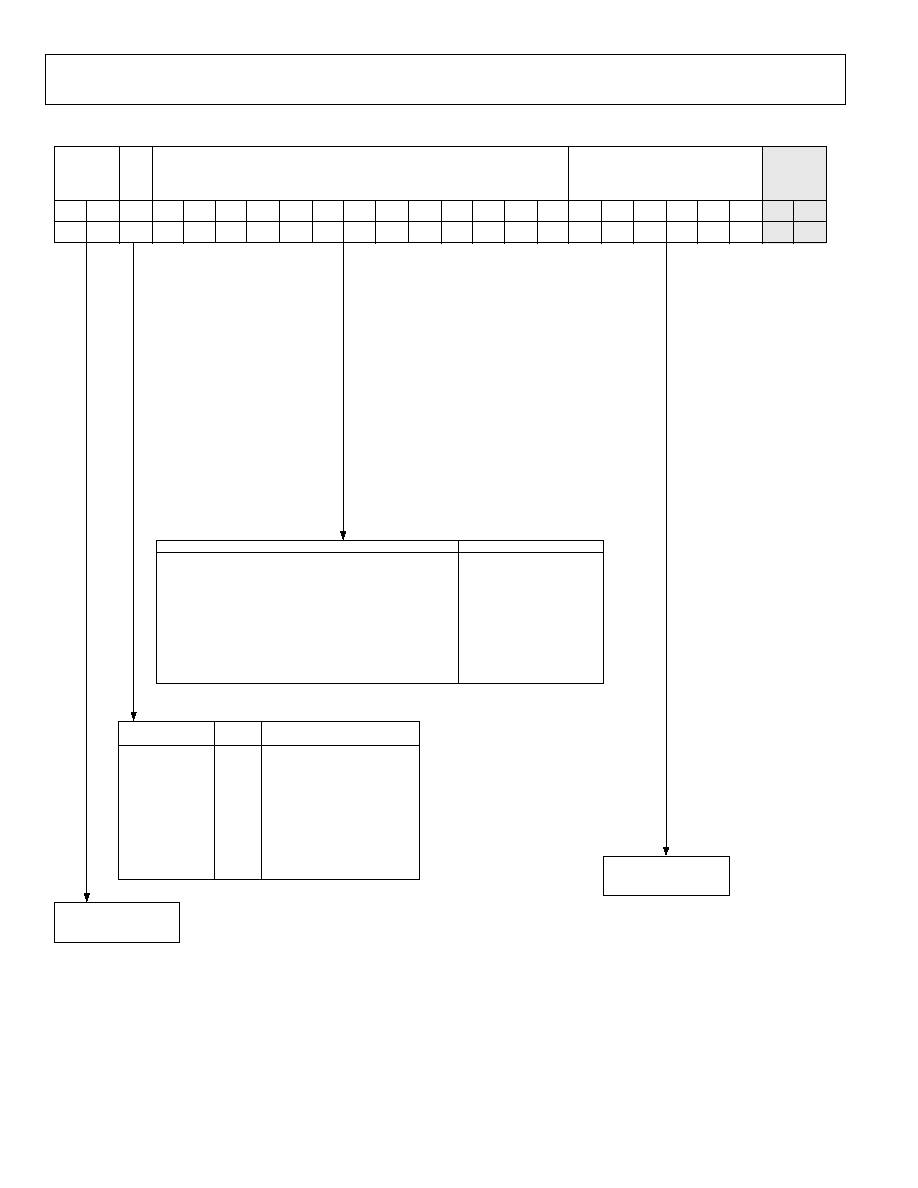
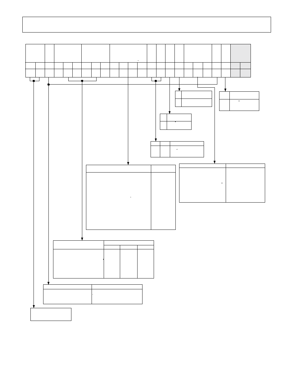
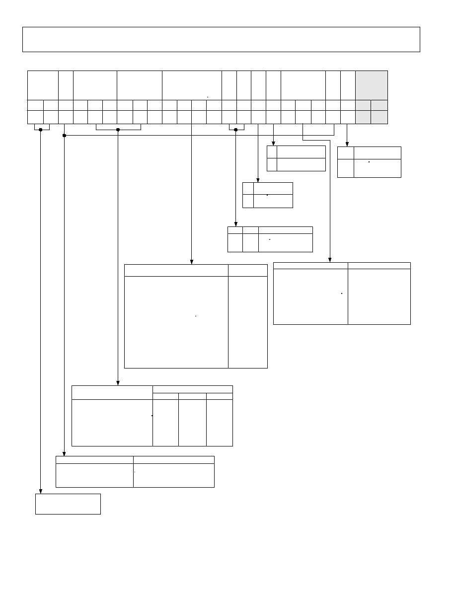
LATCH MAPS AND DESCRIPTIONS
LATCH SUMMARY
DB20 DB19 DB18 DB17 DB16 DB15 DB14 DB13 DB12 DB11 DB10 DB9
DB8
DB7
DB6
DB5
DB4
DB3
DB2
DB1
DB0
C2 (0) C1 (0)
R1
R2
R3
R4
R5
R6
R7
R8
R9
R10
R11
R12
R13
R14
ABP1
ABP2
T1
T2
LDP
DB21
DB22
DB23
0
0
X
DB20 DB19 DB18 DB17 DB16 DB15 DB14 DB13 DB12 DB11 DB10 DB9
DB8
DB7
DB6
DB5
DB4
DB3
DB2
DB1
DB0
C2 (0) C1 (1)
B1
B2
B3
B4
B5
B6
B7
B8
B9
B10
B11
B12
B13
X
X
X
X
X
X
DB21
DB22
DB23
G1
DB20 DB19 DB18 DB17 DB16 DB15 DB14 DB13 DB12 DB11 DB10 DB9
DB8
DB7
DB6
DB5
DB4
DB3
DB2
DB1
DB0
C2 (1) C1 (0)
F1
PD1
M1
M2
M3
F3
X
X
CPI1
CPI2
CPI5
CPI6
TC4
PD2
F2
CPI3
CPI4
DB21
TC3
TC2
TC1
DB22
DB23
F4
F5
DB20 DB19 DB18 DB17 DB16 DB15 DB14 DB13 DB12 DB11 DB10 DB9
DB8
DB7
DB6
DB5
DB4
DB3
DB2
DB1
DB0
C2 (1) C1 (1)
F1
PD1
M1
M2
M3
F3
X
X
CPI1
CPI2
CPI5
CPI6
TC4
PD2
F2
CPI3
CPI4
DB21
TC3
TC2
TC1
DB22
DB23
F4
F5
REFERENCE COUNTER LATCH
RESERVED
LO
C
K
DE
T
E
CT
P
R
E
C
IS
ION
TEST
MODE BITS
ANTI-
BACKLASH
WIDTH
14-BIT REFERENCE COUNTER
CONTROL
BITS
RESERVED
13-BIT N COUNTER
RESERVED
CONTROL
BITS
N COUNTER LATCH
CP
G
A
I
N
FUNCTION LATCH
PO
W
E
R
-
DO
W
N 2
CURRENT
SETTING
2
CURRENT
SETTING
1
TIMER COUNTER
CONTROL
FA
S
T
L
O
C
K
MO
D
E
FA
S
T
L
O
C
K
E
NABL
E
C
P
T
H
R
EE-
ST
A
T
E
PD
P
O
L
ARI
TY
MUXOUT
CONTROL
PO
W
E
R
-
DO
W
N 1
CO
UN
T
E
R
RE
S
E
T
CONTROL
BITS
RESERVED
PO
W
ER
-
DO
W
N 2
CURRENT
SETTING
2
CURRENT
SETTING
1
TIMER COUNTER
CONTROL
FA
S
T
L
O
C
K
MO
D
E
FA
S
T
L
O
C
K
E
NABL
E
C
P
T
HRE
E
-
ST
A
T
E
PD
P
O
L
ARI
T
Y
MUXOUT
CONTROL
PO
W
E
R
-
DO
W
N
1
CO
UN
T
E
R
RE
S
E
T
CONTROL
BITS
INITIALIZATION LATCH
RESERVED
06
05
2-
01
5
Figure 16. Latch Summary
ADF4002
Rev. 0 | Page 11 of 24
REFERENCE COUNTER LATCH MAP
LDP
0
1
ABP2
ABP1
0
0
2.9ns
0
1
1.3ns
1
0
6.0ns
1
1
2.9ns
R14
R13
R12
..........
R3
R2
R1
0
0
0
..........
0
0
1
1
0
0
0
..........
0
1
0
2
0
0
0
..........
0
1
1
3
0
0
0
..........
1
0
0
4
.
.
.
..........
.
.
.
.
.
.
.
..........
.
.
.
.
.
.
.
..........
.
.
.
.
1
1
1
..........
1
0
0
16380
1
1
1
..........
1
0
1
16381
1
1
1
..........
1
1
0
16382
1
1
1
..........
1
1
1
16383
X
= DON'T CARE
DB20 DB19 DB18 DB17 DB16 DB15 DB14 DB13 DB12 DB11 DB10
DB9
DB8
DB7
DB6
DB5
DB4
DB3
DB2
DB1
DB0
C2 (0) C1 (0)
R1
R2
R3
R4
R5
R6
R7
R8
R9
R10
R11
R12
R13
R14
ABP1
ABP2
T1
T2
LDP
DB21
DB22
DB23
0
0
X
RESERVED
LOC
K
DE
T
E
CT
P
R
E
C
IS
ION
TEST
MODE BITS
ANTI-
BACKLASH
WIDTH
14-BIT REFERENCE COUNTER
CONTROL
BITS
DIVIDE RATIO
ANTIBACKLASH PULSEWIDTH
TEST MODE BITS
SHOULD BE SET
TO 00 FOR NORMAL
OPERATION.
OPERATION
THREE CONSECUTIVE CYCLES OF PHASE DELAY LESS THAN
15ns MUST OCCUR BEFORE LOCK DETECT IS SET.
FIVE CONSECUTIVE CYCLES OF PHASE DELAY LESS THAN
15ns MUST OCCUR BEFORE LOCK DETECT IS SET.
BOTH OF THESE BITS
MUST BE SET TO 0 FOR
NORMAL OPERATION.
06
05
2-
0
25
Figure 17. Reference Counter Latch Map
ADF4002
Rev. 0 | Page 12 of 24
N COUNTER LATCH MAP
DB20
DB19
DB18
DB17
DB16
DB15
DB14
DB13
DB12
DB11
DB10
DB9
DB8
DB7
DB6
DB5
DB4
DB3
DB2
DB1
DB0
C2 (0) C1 (1)
B1
B2
B3
B4
B5
B6
B7
B8
B9
B10
B11
B12
B13
X
X
X
X
X
X
DB21
DB22
DB23
G1
0
0
0
1
1
0
F4 (FUNCTION LATCH)
FASTLOCK ENABLE
1
1
X
X
N13
N12
N11
N3
N2
N1
0
0
0
..........
0
0
0
0
0
0
..........
0
0
1
0
0
0
..........
0
1
0
0
0
0
..........
0
1
1
3
.
.
.
..........
.
.
.
.
.
.
.
..........
.
.
.
.
.
.
.
..........
.
.
.
.
1
1
1
..........
1
0
0
8188
1
1
1
..........
1
0
1
8189
1
1
1
..........
1
1
0
8190
1
1
1
..........
1
1
1
8191
X = DON'T CARE
RESERVED
13-BIT N COUNTER
RESERVED
CONTROL
BITS
C
P
G
A
IN
N COUNTER DIVIDE RATIO
NOT ALLOWED
1
2
THESE BITS ARE NOT USED
BY THE DEVICE AND ARE
DON'T CARE BITS.
OPERATION
CP GAIN
CHARGE PUMP CURRENT
SETTING 1 IS PERMANENTLY USED.
CHARGE PUMP CURRENT
SETTING 2 IS PERMANENTLY USED.
CHARGE PUMP CURRENT
SETTING 1 IS USED.
CHARGE PUMP CURRENT IS
SWITCHED TO SETTING 2. THE
TIME SPENT IN SETTING 2 IS
DEPENDENT ON WHICH FASTLOCK
MODE IS USED. SEE FUNCTION
LATCH DESCRIPTION.
THESE BITS ARE NOT USED
BY THE DEVICE AND ARE
DON'T CARE BITS.
06
05
2-
016
Figure 18. N Counter Latch Map
ADF4002
Rev. 0 | Page 13 of 24
FUNCTION LATCH MAP
PD2
PD1
MODE
0
X
X
1
X
0
1
0
1
1
1
1
CPI6
CPI5
CP14
CPI3
CPI2
CPI1
3k
5.1k
11k
0
0
0
0
0
1
0
1
0
0
1
1
1
0
0
1
0
1
1
1
0
1
1
1
TC4
TC3
TC2
TC1
0
0
0
0
3
0
0
0
1
7
0
0
1
0
11
0
0
1
1
15
0
1
0
0
19
0
1
0
1
23
0
1
1
0
27
0
1
1
1
31
1
0
0
0
35
1
0
0
1
39
1
0
1
0
43
1
0
1
1
47
1
1
0
0
51
1
1
0
1
55
1
1
1
0
59
1
1
1
1
63
F4
0
1
1
M3
M2
M1
0
0
0
0
0
1
0
1
0
0
1
1
1
0
0
1
0
1
1
1
0
1
1
1
F3
0
1
F2
0
1
F1
0
1
DB20 DB19 DB18 DB17 DB16 DB15 DB14 DB13 DB12 DB11 DB10 DB9
DB8
DB7
DB6
DB5
DB4
DB3
DB2
DB1
DB0
C2 (1) C1 (0)
F1
PD1
M1
M2
M3
F3
P1
P2
CPI1
CPI2
CPI5
CPI6
TC4
PD2
F2
CPI3
CPI4
DB21
TC3
TC2
TC1
DB22
DB23
F4
F5
THREE-STATE
F5
X
0
1
NEGATIVE
POSITIVE
RESERVED
PO
W
ER
-
DO
W
N 2
CURRENT
SETTING
2
CURRENT
SETTING
1
TIMER COUNTER
CONTROL
FA
S
T
L
O
C
K
MO
D
E
FA
S
T
L
O
C
K
E
NABL
E
CP
T
H
R
EE-
S
TAT
E
MUXOUT
CONTROL
PO
W
ER
-
DO
W
N 1
CO
UNT
E
R
R
ESET
CONTROL
BITS
PHASE DETECTOR
POLARITY
COUNTER
OPERATION
NORMAL
R, A, B COUNTERS
HELD IN RESET
CHARGE PUMP
OUTPUT
NORMAL
FASTLOCK DISABLED
FASTLOCK MODE 1
FASTLOCK MODE 2
FASTLOCK MODE
THREE-STATE OUTPUT
DIGITAL LOCK DETECT
(ACTIVE HIGH)
N DIVIDER OUTPUT
DV
DD
R DIVIDER OUTPUT
N-CHANNEL OPEN-DRAIN
LOCK DETECT
SERIAL DATA OUTPUT
DGND
OUTPUT
TIMEOUT
(PFD CYCLES)
I
CP
(mA)
ASYNCHRONOUS POWER-DOWN
NORMAL OPERATION
ASYNCHRONOUS POWER-DOWN
SYNCHRONOUS POWER-DOWN
CE PIN
PD
PO
L
ARI
TY
06052-
017
THESE BITS ARE NOT USED
BY THE DEVICE AND ARE
DON'T CARE BITS.
1.088
2.176
3.264
4.352
5.440
6.528
7.616
8.704
0.625
1.250
1.875
2.500
3.125
3.750
4.375
5.000
0.294
0.588
0.882
1.176
1.470
1.764
2.058
2.352
SEE PAGE 16
Figure 19. Function Latch Map
ADF4002
Rev. 0 | Page 14 of 24
INITIALIZATION LATCH MAP
PD2
PD1
MODE
0
X
X
1
X
0
1
0
1
1
1
1
CPI6
CPI5
CP14
CPI3
CPI2
CPI1
3k
5.1k
11k
0
0
0
0
0
1
0
1
0
0
1
1
1
0
0
1
0
1
1
1
0
1
1
1
TC4
TC3
TC2
TC1
0
0
0
0
3
0
0
0
1
7
0
0
1
0
11
0
0
1
1
15
0
1
0
0
19
0
1
0
1
23
0
1
1
0
27
0
1
1
1
31
1
0
0
0
35
1
0
0
1
39
1
0
1
0
43
1
0
1
1
47
1
1
0
0
51
1
1
0
1
55
1
1
1
0
59
1
1
1
1
63
F4
0
1
1
M3
M2
M1
0
0
0
0
0
1
0
1
0
0
1
1
1
0
0
1
0
1
1
1
0
1
1
1
F3
0
1
F2
0
1
F1
0
1
DB20 DB19 DB18 DB17 DB16 DB15 DB14 DB13 DB12 DB11 DB10 DB9
DB8
DB7
DB6
DB5
DB4
DB3
DB2
DB1
DB0
C2 (1) C1 (1)
F1
PD1
M1
M2
M3
F3
P1
P2
CPI1
CPI2
CPI5
CPI6
TC4
PD2
F2
CPI3
CPI4
DB21
TC3
TC2
TC1
DB22
DB23
F4
F5
THREE-STATE
F5
X
0
1
NEGATIVE
POSITIVE
RESERVED
PO
W
ER
-
DO
W
N 2
CURRENT
SETTING
2
CURRENT
SETTING
1
TIMER COUNTER
CONTROL
FA
S
T
L
O
C
K
MO
D
E
FA
S
T
L
O
C
K
E
NABL
E
CP
T
H
R
EE-
S
TAT
E
MUXOUT
CONTROL
PO
W
ER
-
DO
W
N 1
CO
UNT
E
R
R
ESET
CONTROL
BITS
PHASE DETECTOR
POLARITY
COUNTER
OPERATION
NORMAL
R, A, B COUNTERS
HELD IN RESET
CHARGE PUMP
OUTPUT
NORMAL
FASTLOCK DISABLED
FASTLOCK MODE 1
FASTLOCK MODE 2
FASTLOCK MODE
THREE-STATE OUTPUT
DIGITAL LOCK DETECT
(ACTIVE HIGH)
N DIVIDER OUTPUT
DV
DD
R DIVIDER OUTPUT
N-CHANNEL OPEN-DRAIN
LOCK DETECT
SERIAL DATA OUTPUT
DGND
OUTPUT
TIMEOUT
(PFD CYCLES)
I
CP
(mA)
ASYNCHRONOUS POWER-DOWN
NORMAL OPERATION
ASYNCHRONOUS POWER-DOWN
SYNCHRONOUS POWER-DOWN
CE PIN
PD
PO
L
ARI
TY
06052-
036
THESE BITS ARE NOT USED
BY THE DEVICE AND ARE
DON'T CARE BITS.
1.088
2.176
3.264
4.352
5.440
6.528
7.616
8.704
0.625
1.250
1.875
2.500
3.125
3.750
4.375
5.000
0.294
0.588
0.882
1.176
1.470
1.764
2.058
2.352
SEE PAGE 16
Figure 20. Initialization Latch Map

ADF4002
Rev. 0 | Page 15 of 24
THE FUNCTION LATCH
With C2, C1 set to 1, 0, the on-chip function latch is
programmed. Figure 19 shows the input data format for
programming the function latch.
Counter Reset
DB2 (F1) is the counter reset bit. When this bit is set to 1, the
R counter and the N counters are reset. For normal operation,
set this bit to 0. Upon powering up, the F1 bit needs to be
disabled (set to 0). Then, the N counter resumes counting in
close alignment with the R counter (the maximum error is one
prescaler cycle).
Power-Down
DB3 (PD1) and DB21 (PD2) provide programmable power-
down modes. These bits are enabled by the CE pin.
When the CE pin is low, the device is immediately disabled
regardless of the states of the PD2, PD1 bits.
In the programmed asynchronous power-down, the device
powers down immediately after latching a 1 into Bit PD1, with
the condition that Bit PD2 has been loaded with a 0.
In the programmed synchronous power-down, the device
power-down is gated by the charge pump to prevent unwanted
frequency jumps. Once the power-down is enabled by writing
a 1 into Bit PD1 (on condition that a 1 has also been loaded to
Bit PD2), then the device enters power-down on the occurrence
of the next charge pump event.
When a power-down is activated (either in synchronous or
asynchronous mode, including a CE pin activated power-
down), the following events occur:
·
All active dc current paths are removed.
·
The R, N, and timeout counters are forced to their load-
state conditions.
·
The charge pump is forced into three-state mode.
·
The digital lock detect circuitry is reset.
·
The RFIN input is debiased.
·
The reference input buffer circuitry is disabled.
·
The input register remains active and capable of loading
and latching data.
MUXOUT Control
The on-chip multiplexer is controlled by M3, M2, and M1 on
the ADF4002. Figure 19 shows the truth table.
Fastlock Enable Bit
DB9 of the function latch is the fastlock enable bit. Only when
this is 1 is fastlock enabled.
Fastlock Mode Bit
DB10 of the function latch is the fastlock mode bit. When
fastlock is enabled, this bit determines the fastlock mode to be
used. If the fastlock mode bit is 0, then Fastlock Mode 1 is
selected, and if the fastlock mode bit is 1, then Fastlock Mode 2
is selected.
Fastlock Mode 1
In this mode, the charge pump current is switched to the
contents of Current Setting 2. The device enters fastlock by
having a 1 written to the CP gain bit in the N counter latch. The
device exits fastlock by having a 0 written to the CP gain bit in
the AB counter latch.
Fastlock Mode 2
In this mode, the charge pump current is switched to the
contents of Current Setting 2. The device enters fastlock by
having a 1 written to the CP gain bit in the N counter latch. The
device exits fastlock under the control of the timer counter.
After the timeout period determined by the value in TC4 to
TC1, the CP gain bit in the N counter latch is automatically
reset to 0 and the device reverts to normal mode instead of
fastlock. See Figure 19 for the timeout periods.
Timer Counter Control
The user has the option of programming two charge pump
currents. The intent is to use the Current Setting 1 when the RF
output is stable and the system is in a static state. Current
Setting 2 is meant to be used when the system is dynamic and in
a state of change, that is, when a new output frequency is
programmed.
The normal sequence of events is as follows:
The user initially decides the referred charge pump currents.
For example, the choice can be 2.5 mA as Current Setting 1 and
5 mA as Current Setting 2.
At the same time, the decision must be made as to how long the
secondary current is to stay active before reverting to the
primary current. This is controlled by Timer Counter Control
Bit DB14 to Timer Counter Control Bit DB11 (TC4 to TC1) in
the function latch. See Figure 19 for the truth table.
To program a new output frequency, simply program the N
counter latch with a new value for N. At the same time, the CP
gain bit can be set to 1. This sets the charge pump with the
value in CPI6 to CPI4 for a period of time determined by TC4
to TC1. When this time is up, the charge pump current reverts
to the value set by CPI3 to CPI1. At the same time, the CP gain
bit in the N counter latch is reset to 0 and is ready for the next
time that the user wishes to change the frequency.
Note that there is an enable feature on the timer counter. It is
enabled when Fastlock Mode 2 is chosen by setting the Fastlock
Mode Bit DB10 in the function latch to 1.

ADF4002
Rev. 0 | Page 16 of 24
Charge Pump Currents
CPI3, CPI2, and CPI1 program Current Setting 1 for the charge
pump. CPI6, CPI5, and CPI4 program Current Setting 2 for the
charge pump. See Figure 19 for the truth table.
PD Polarity
This bit sets the phase detector polarity bit (see Figure 19).
CP Three-State
This bit controls the CP output pin. Setting the bit high, puts
the CP output into three-state. With the bit set low, the CP
output is enabled.
THE INITIALIZATION LATCH
The initialization latch is programmed when C2, C1 = 1, 1. This
is essentially the same as the function latch (programmed when
C2, C1 = 1, 0).
However, when the initialization latch is programmed there is
an additional internal reset pulse applied to the R and N
counters. This pulse ensures that the N counter is at load point
when the N counter data is latched and the device begins
counting in close phase alignment.
If the latch is programmed for synchronous power-down (CE
pin is high; PD1 bit is high; and PD2 bit is low), the internal
pulse also triggers this power-down. The prescaler reference
and the oscillator input buffer are unaffected by the internal
reset pulse, thereby maintaining close phase alignment when
counting resumes.
When the first N counter data is latched after initialization, the
internal reset pulse is reactivated. However, successive AB
counter loads after this do not trigger the internal reset pulse.
Device Programming After Initial Power-Up
After initially powering up the device, there are three ways to
program the device.
Initialization Latch Method
1.
Apply V
DD
.
2.
Program the initialization latch (11 in two LSBs of input
word). Make sure that the F1 bit is programmed to 0.
3.
Conduct a function latch load (10 in two LSBs of the
control word). Make sure that the F1 bit is programmed to 0.
4.
Perform an R load (00 in two LSBs).
5.
Perform an N load (01 in two LSBs).
When the initialization latch is loaded, the following occurs:
·
The function latch contents are loaded.
·
An internal pulse resets the R, N, and timeout counters to
load-state conditions and three-states the charge pump.
Note that the prescaler band gap reference and the
oscillator input buffer are unaffected by the internal reset
pulse, allowing close phase alignment when counting
resumes.
·
Latching the first N counter data after the initialization
word activates the same internal reset pulse. Successive N
loads do not trigger the internal reset pulse unless there is
another initialization.
CE Pin Method
1.
Apply V
DD
.
2.
Bring CE low to put the device into power-down. This is an
asynchronous power-down because it happens
immediately.
3.
Program the function latch (10).
4.
Program the R counter latch (00).
5.
Program the N counter latch (01).
6.
Bring CE high to take the device out of power-down. The
R and N counters resume counting in close alignment.
Note that after CE goes high, a duration of 1 s can be
required for the prescaler band gap voltage and oscillator
input buffer bias to reach steady state.
CE can be used to power the device up and down to check for
channel activity. The input register does not need to be
reprogrammed each time the device is disabled and enabled, as
long as it has been programmed at least once after V
DD
was
initially applied.
Counter Reset Method
1.
Apply V
DD
.
2.
Do a function latch load (10 in two LSBs). As part of this
step, load 1 to the F1 bit. This enables the counter reset.
3.
Perform an R counter load (00 in two LSBs).
4.
Perform an N counter load (01 in two LSBs).
5.
Do a function latch load (10 in two LSBs). As part of this
step, load 0 to the F1 bit. This disables the counter reset.
This sequence provides the same close alignment as the
initialization method. It offers direct control over the internal
reset. Note that counter reset holds the counters at load point
and three-states the charge pump, but does not trigger
synchronous power-down.
ADF4002
Rev. 0 | Page 17 of 24
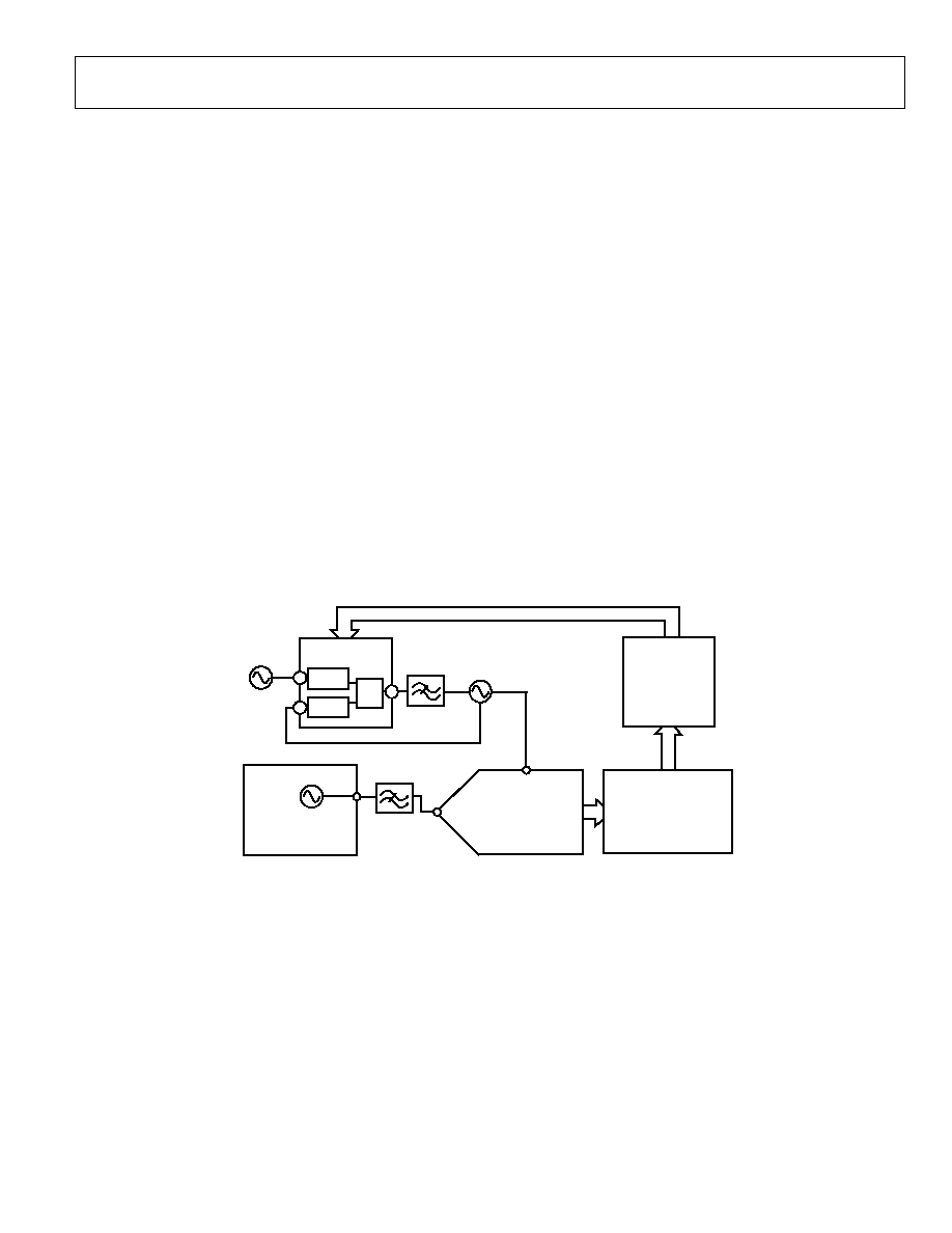
APPLICATIONS
VERY LOW JITTER ENCODE CLOCK FOR HIGH
SPEED CONVERTERS
Figure 21 shows the ADF4002 with a VCXO to provide the
encode clock for a high speed analog-to-digital converter (ADC).
The converter used in this application is an
AD9215-80
, a 12-bit
converter that accepts up to an 80 MHz encode clock. To realize
a stable low jitter clock, use a 77.76 MHz, narrow band VCXO.
This example assumes a 19.44 MHz reference clock.
To minimize the phase noise contribution of the ADF4002, the
smallest multiplication factor of 4 is used. Thus, the R divider is
programmed to 1, and the N divider is programmed to 4.
The charge pump output of the ADF4002 (Pin 2) drives the
loop filter. The loop filter bandwidth is optimized for the best
possible rms jitter, a key factor in the signal-to-noise ratio
(SNR) of the ADC. Too narrow a bandwidth allows the VCXO
noise to dominate at small offsets from the carrier frequency.
Too wide a bandwidth allows the ADF4002 noise to dominate at
offsets where the VCXO noise is lower than the ADF4002 noise.
Thus, the intersection of the VCXO noise and the ADF4002 in-
band noise is chosen as the optimum loop filter bandwidth.
The design of the loop filter uses the ADIsimPLL (Version 3.0)
and is available as a free download from
www.analog.com/pll
.
The rms jitter is measured at <1.2 ps. This level is lower than
the maximum allowable 6 ps rms required to ensure the
theoretical SNR performance of 59 dB for this converter.
The setup shown in Figure 21 using the ADF4002, AD9215, and
HSC-ADC-EVALA-SC, allows the user to quickly and
effectively determine the suitability of the converter and encode
clock. The SPI® interface is used to control the ADF4002, and
the USB interface helps control the operation of the AD9215-
80. The controller board sends back FFT information to the PC
that, if using an ADC analyzer, provides all conversion results
from the ADC.
VCXO: 77.76MHz
HC-ADC-EVALA-SC
PC
US
B
TCXO:
19.44MHz
ENCODE
CLOCK
A
IN
ADF4002
N = 4
PD
R = 1
SPI
AGILENT:
500kHz, 1.8V p-p
0605
2-
034
AD9215-80
Figure 21. ADF4002 as Encode Clock
ADF4002
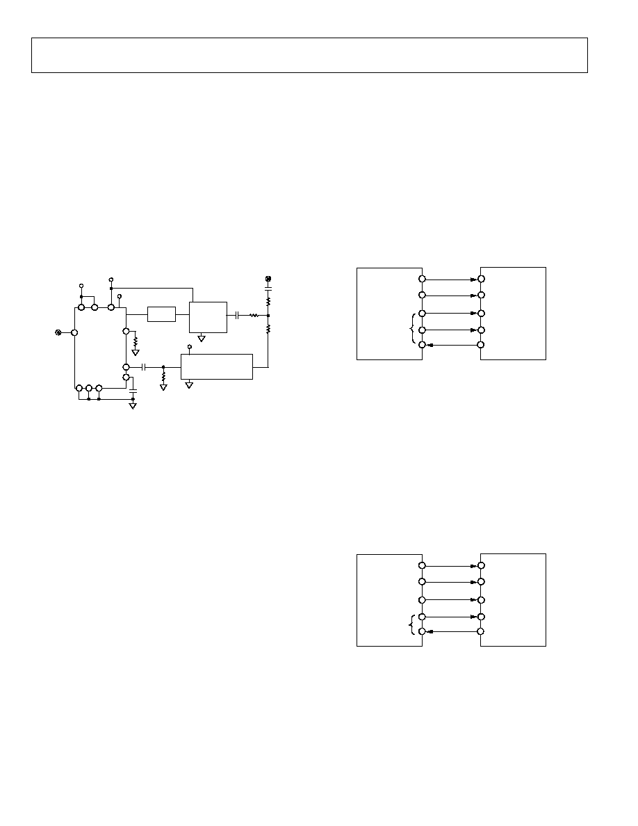
Rev. 0 | Page 18 of 24
PFD
As the ADF4002 permits both R and N counters to be
programmed to 1, the part can effectively be used as a stand
alone PFD and charge pump. This is particularly useful in either
a clock cleaning application or a high performance LO. Addi-
tionally, the very low normalized phase noise floor (-222 dBc/Hz)
enables very low in-band phase noise levels. It is possible to
operate the PFD up to a maximum frequency of 200 MHz.
In Figure 22, the reference frequency equals the PFD, therefore,
R = 1. The charge pump output integrates into a stable control
voltage for the VCXO, and the output from the VCXO is
divided down to the desired PFD frequency using an external
divider.
06052-
035
8
2
16
15
7
6
5
9
4
3
1
REF
IN
REF
IN
R
SET
RF
IN
A
RF
IN
B
AV
DD
DV
DD
CP
G
ND
AG
ND
DG
ND
V
DD
V
P
V
P
CE
ADF4002
DECOUPLING CAPACITORS AND
INTERFACE SIGNALS HAVE BEEN
OMITTED FROM THE DIAGRAM IN
THE INTERESTS OF GREATER
CLARITY.
100pF
100pF
51
10k
LOOP
FILTER
GND
VCO
OR
VCXO
V
CC
GND
EXTERNAL PRESCALER
18
18
18
100pF
100pF
RF
OUT
V
CC
V
CC
Figure 22. ADF4002 as a PFD
INTERFACING
The ADF4002 has a simple SPI-compatible serial interface for
writing to the device. CLK, DATA, and LE control the data
transfer. When the latch enable (Pin LE) goes high, the 24 bits
that have been clocked into the input register on each rising
edge of CLK are transferred to the appropriate latch. For more
information, see Figure 2 for the timing diagram and Table 6 for
the latch truth table.
The maximum allowable serial clock rate is 20 MHz. This
means that the maximum update rate possible for the device is
833 kHz, or one update every 1.2 s. This is certainly more than
adequate for systems that have typical lock times in hundreds of
microseconds.
ADuC812 Interface
Figure 23 shows the interface between the ADF4002 and the
ADuC812
MicroConverter®. Since the
ADuC812
is based on an
8051 core, this interface can be used with any 8051-based
microcontroller. The MicroConverter is set up for SPI master
mode with CPHA = 0. To initiate the operation, the I/O port
driving LE is brought low. Each latch of the ADF4002 needs a
24-bit word. This is accomplished by writing three, 8-bit bytes
from the MicroConverter to the device. When the third byte
has been written, bring the LE input high to complete the
transfer.
On first applying power to the ADF4002, it needs four writes
(one each to the initialization latch, function latch, R counter
latch, and N counter latch) for the output to become active.
I/O port lines on the
ADuC812
are also used to control power-
down (CE input) and to detect lock (MUXOUT configured as
lock detect and polled by the port input).
When operating in the SPI master mode, the maximum
SCLOCK rate of the
ADuC812
is 4 MHz. This means that the
maximum rate at which the output frequency can be changed is
166 kHz.
CLK
DATA
LE
CE
MUXOUT
(LOCK DETECT)
MOSI
SCLOCK
I/O PORTS
ADuC812
ADF4002
06
05
2-
01
9
Figure 23. ADuC812 to ADF4002 Interface
ADSP2181 Interface
Figure 24 shows the interface between the ADF4002 and the
ADSP21xx digital signal processor. The ADF4002 needs a
24-bit serial word for each latch write. The easiest way to
accomplish this using the ADSP21xx family is to use the
autobuffered transmit mode of operation with alternate
framing. This provides a means for transmitting an entire block
of serial data before an interrupt is generated. Set up the word
length for 8 bits and use three memory locations for each 24-bit
word. To program each 24-bit latch, store the three 8-bit bytes,
enable the autobuffered mode, and then write to the transmit
register of the DSP. This last operation initiates the autobuffer
transfer.
CLK
DATA
LE
CE
MUXOUT
(LOCK DETECT)
ADSP21xx
ADF4002
DT
SCLK
I/O FLAGS
TFS
06
05
2-
0
20
Figure 24. ADSP-21xx to ADF4002 Interface
PCB DESIGN GUIDELINES FOR CHIP SCALE
PACKAGE
The lands on the lead frame chip scale package (CP-20-1) are
rectangular. The printed circuit board pad for these should be
0.1 mm longer than the package land length and 0.05 mm wider
than the package land width. The land should be centered on
the pad. This ensures that the solder joint size is maximized.

ADF4002
Rev. 0 | Page 19 of 24
The bottom of the lead frame chip scale package has a central
thermal pad.
The thermal pad on the printed circuit board should be at least
as large as this exposed pad. On the printed circuit board, there
should be a clearance of at least 0.25 mm between the thermal
pad and the inner edges of the pad pattern. This ensures that
shorting is avoided.
Thermal vias can be used on the printed circuit board thermal
pad to improve thermal performance of the package. If vias are
used, they should be incorporated in the thermal pad at a 1.2 mm
pitch grid. The via diameter should be between 0.3 mm and
0.33 mm and the via barrel should be plated with 1 oz. copper
to plug the via.
The user should connect the printed circuit board thermal pad
to AGND.
ADF4002
Rev. 0 | Page 20 of 24
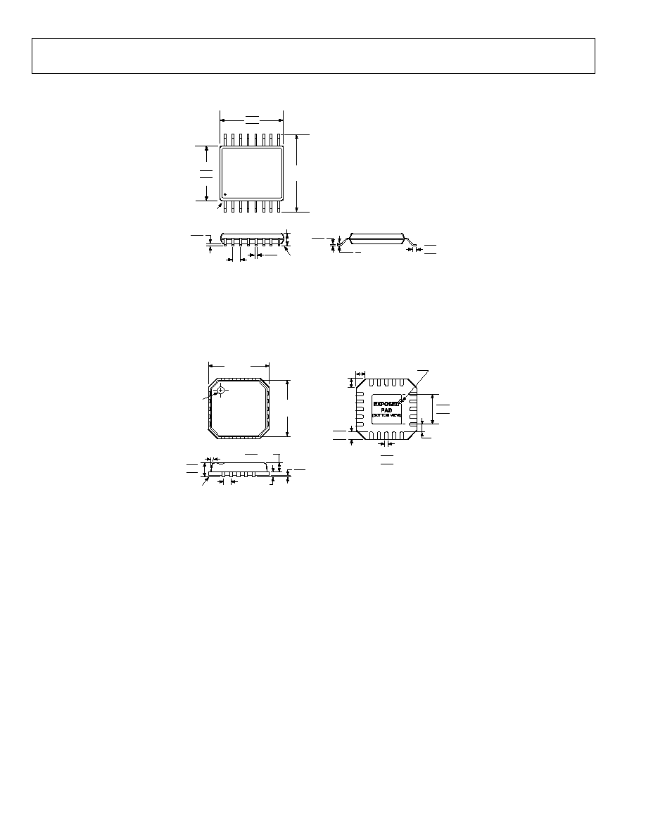
OUTLINE DIMENSIONS
16
9
8
1
PIN 1
SEATING
PLANE
8°
0°
4.50
4.40
4.30
6.40
BSC
5.10
5.00
4.90
0.65
BSC
0.15
0.05
1.20
MAX
0.20
0.09
0.75
0.60
0.45
0.30
0.19
COPLANARITY
0.10
COMPLIANT TO JEDEC STANDARDS MO-153-AB
Figure 25. 16-Lead Thin Shrink Small Outline Package [TSSOP]
(RU-16)
Dimensions shown in millimeters
1
20
5
6
11
16
15
10
2.25
2.10 SQ
1.95
0.75
0.55
0.35
0.30
0.23
0.18
0.50
BSC
12° MAX
0.20
REF
0.80 MAX
0.65 TYP
0.05 MAX
0.02 NOM
1.00
0.85
0.80
SEATING
PLANE
PIN 1
INDICATOR
TOP
VIEW
3.75
BCS SQ
4.00
BSC SQ
COPLANARITY
0.08
0.60
MAX
0.60
MAX
0.25 MIN
COMPLIANT TO JEDEC STANDARDS MO-220-VGGD-1
PIN 1
INDICATOR
Figure 26. 20-Lead Lead Frame Chip Scale Package [LFCSP_VQ]
(CP-20-1)
Dimensions shown in millimeters

ADF4002
Rev. 0 | Page 21 of 24
ORDERING GUIDE
Model
Temperature Range
Package Description
Package Option
ADF4002BRUZ
1
40°C to +85°C
16-Lead TSSOP
RU-16
ADF4002BRUZRL
1
40°C to +85°C
16-Lead TSSOP
RU-16
ADF4002BRUZRL7
1
40°C to +85°C
16-Lead TSSOP
RU-16
ADF4002BCPZ
1
40°C to +85°C
20-Lead LFCSP_VQ
CP-20-1
ADF4002BCPZRL
1
40°C to +85°C
20-Lead LFCSP_VQ
CP-20-1
ADF4002BCPZRL7
1
40°C to +85°C
20-Lead LFCSP_VQ
CP-20-1
EVAL-ADF4002EB1
Evaluation
Board
EVAL-ADF411XEB1
Evaluation
Board
1
Z = Pb-free part.

ADF4002
Rev. 0 | Page 22 of 24
NOTES

ADF4002
Rev. 0 | Page 23 of 24
NOTES

ADF4002
Rev. 0 | Page 24 of 24
NOTES
©2006 Analog Devices, Inc. All rights reserved. Trademarks and
registered trademarks are the property of their respective owners.
D06052-0-4/06(0)
Document Outline
- þÿ
- þÿ
- þÿ
- þÿ
- þÿ
- þÿ
- þÿ
- þÿ
- þÿ
- þÿ
- þÿ
- þÿ
- þÿ
- þÿ
- þÿ
- þÿ
- þÿ
- þÿ
- þÿ
- þÿ
- þÿ
- þÿ
- þÿ
- þÿ
- þÿ
- þÿ
- þÿ
- þÿ
- þÿ
- þÿ
- þÿ
- Very Low Jitter Encode Clock for High Speed Converters
- PFD
- Interfacing
- ADuC812 Interface
- ADSP2181 Interface
- PCB Design Guidelines for Chip Scale Package
- þÿ