 | ÐлекÑÑоннÑй компоненÑ: ADE7752A | СкаÑаÑÑ:  PDF PDF  ZIP ZIP |
ADE7752/ADE7752A Polyphase Energy Metering IC with Pulse Output Data Sheet (Rev C.)
Polyphase Energy Metering IC
with Pulse Output
ADE7752/ADE7752A
FEATURES
High accuracy, supports 50 Hz/60 Hz IEC62053-2x
Less than 0.1% error over a dynamic range of 500 to 1
Compatible with 3-phase/3-wire delta and 3-phase/4-wire
Wye configurations
The ADE7752
1
supplies average real power on frequency
outputs F1 and F2
High frequency output CF is intended for calibration and
supplies instantaneous real power
Logic output REVP indicates a potential miswiring or
negative power for each phase
Direct drive for electromechanical counters and 2-phase
stepper motors (F1 and F2)
Proprietary ADCs and DSP provide high accuracy over large
variations in environmental conditions and time
On-chip power supply monitoring
On-chip creep protection (no load threshold)
On-chip reference 2.4 V ±8% (20 ppm/°C typical) with
external overdrive capability
Single 5 V supply, low power
60 mW typical: ADE7752
30 mW typical: ADE7752A
Low cost CMOS process
GENERAL DESCRIPTION
The ADE7752 is a high accuracy polyphase electrical energy
measurement IC. The ADE7752A is a pin-to-pin compatible
low power version of ADE7752. The functions of ADE7752 and
ADE7752A are the same. Both products are referred to in the
text of this data sheet as ADE7752.
The part specifications surpass the accuracy requirements as
quoted in the IEC62053-2x standard. The only analog circuitry
used in the ADE7752 is in the analog-to-digital converters (ADCs)
and reference circuit. All other signal processing (such as multi-
plication, filtering, and summation) is carried out in the digital
domain. This approach provides superior stability and accuracy
over extremes in environmental conditions and over time.
The ADE7752 supplies average real power information on the
low frequency outputs, F1 and F2. These logic outputs may be
used to directly drive an electromechanical counter or to
interface with an MCU. The CF logic output gives instanta-
neous real power information. This output is intended to be
used for calibration purposes.
The ADE7752 includes a power supply monitoring circuit on
the V
DD
pin. The ADE7752 remains inactive until the supply
voltage on V
DD
reaches 4 V. If the supply falls below 4 V, no
pulses are issued on F1, F2, and CF. Internal phase matching
circuitry ensures that the voltage and current channels are
phase matched. An internal no load threshold ensures the part
does not exhibit any creep when there is no load. The ADE7752
is available in a 24-lead SOIC package.
1
Patent pending.
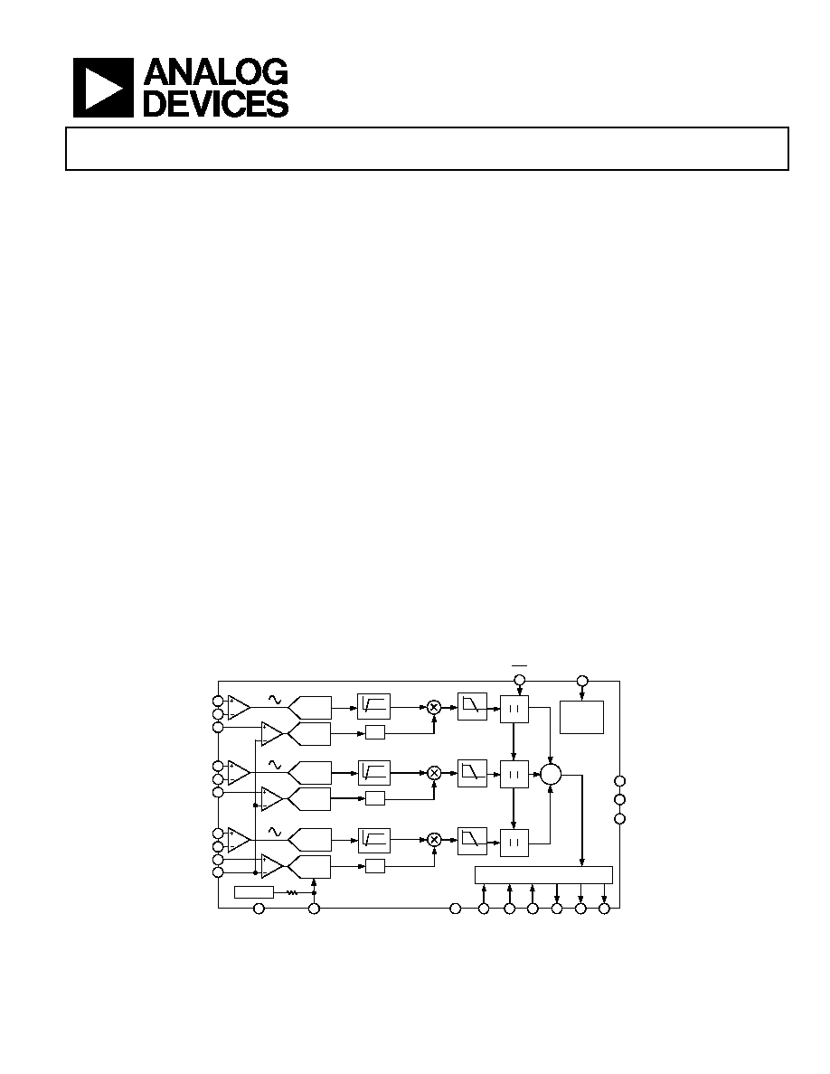
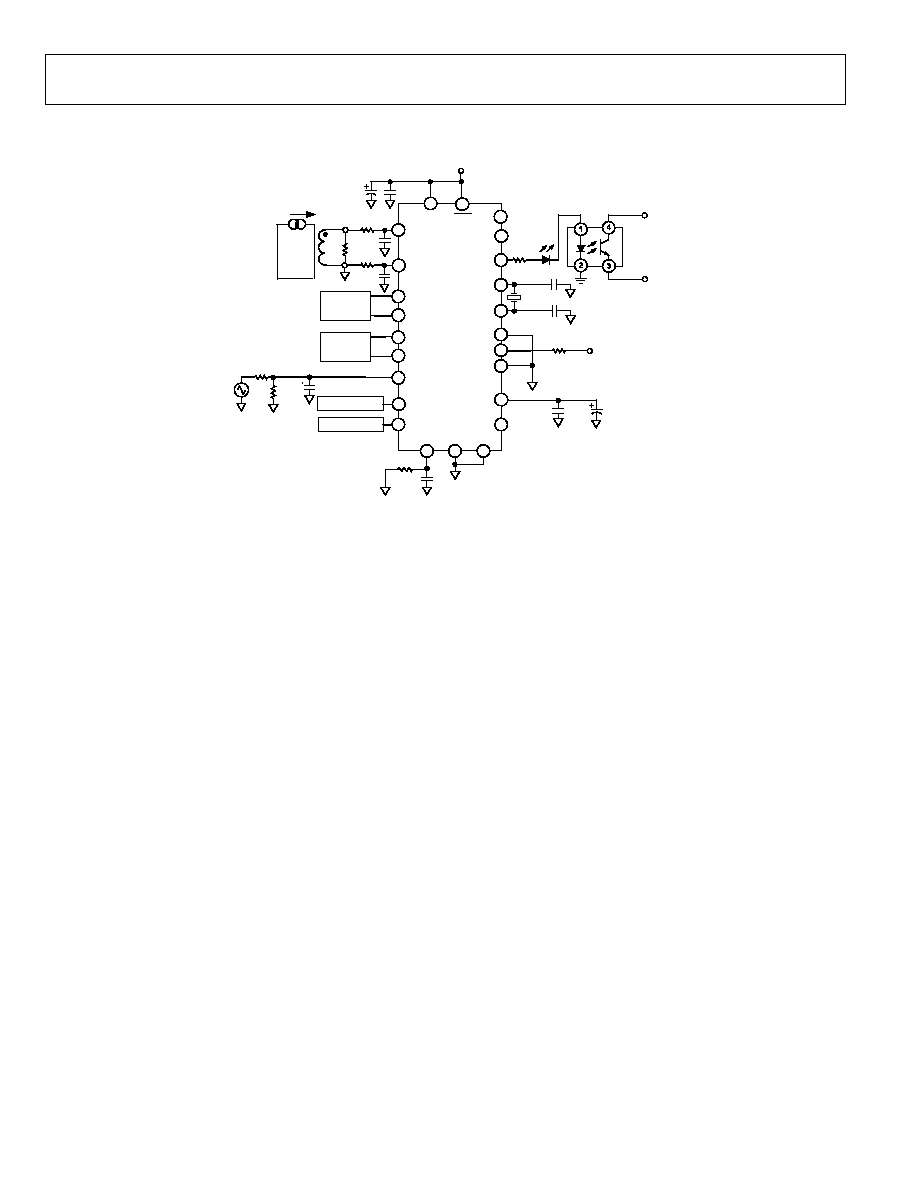
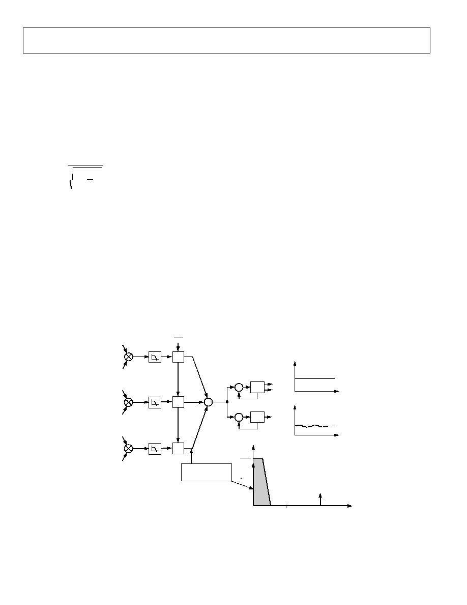
FUNCTIONAL BLOCK DIAGRAM
7
8
15
10
14
13
5
6
16
9
LPF
HPF
3
CLKOUT
CLKIN
DGND
CF
S1
F1
F2
S0
SCF
REVP
DIGITAL-TO-FREQUENCY CONVERTER
2.4V REF
REF
IN/OUT
AGND
4k
IBP
IBN
VBP
VN
ICP
ICN
VCP
IAP
IAN
VAP
ADC
ADC
ADC
ADC
V
DD
ADE7752/
ADE7752A
POWER
SUPPLY
MONITOR
ADC
ADC
PHASE
CORRECTION
PHASE
CORRECTION
PHASE
CORRECTION
11
12
4
18
21
22
23
24
1
20
19
2
17
HPF
HPF
LPF
LPF
ABS
X
X
X
02
67
6-
A
-
0
01
Figure 1. 24-Lead Standard Small Outline Package [SOIC]
Rev. C
Information furnished by Analog Devices is believed to be accurate and reliable. However, no
responsibility is assumed by Analog Devices for its use, nor for any infringements of patents or other
rights of third parties that may result from its use. Specifications subject to change without notice.
No license is granted by implication or otherwise under any patent or patent rights of Analog
Devices. Trademarks and registered trademarks are the property of their respective owners.
One Technology Way, P.O. Box 9106, Norwood, MA 02062-9106, U.S.A.
Tel: 781.329.4700
www.analog.com
Fax: 781.461.3113
© 2005 Analog Devices, Inc. All rights reserved.

ADE7752/ADE7752A
Rev. C | Page 2 of 24
TABLE OF CONTENTS
Specifications..................................................................................... 3
Timing Characteristics..................................................................... 4
Absolute Maximum Ratings............................................................ 5
ESD Caution.................................................................................. 5
Pin Configuration and Function Descriptions............................. 6
Typical Performance Characteristics ............................................. 8
Test Circuit ...................................................................................... 10
Terminology .................................................................................... 11
Theory of Operation ...................................................................... 12
Power Factor Considerations.................................................... 12
Nonsinusoidal Voltage and Current ........................................ 13
Analog Inputs.................................................................................. 14
Current Channels ....................................................................... 14
Voltage Channels ........................................................................ 14
Typical Connection Diagrams ...................................................... 15
Current Channel Connection ................................................... 15
Voltage Channels Connection .................................................. 15
Meter Connections..................................................................... 15
Power Supply Monitor ................................................................... 17
HPF and Offset Effects .............................................................. 17
Digital-to-Frequency Conversion ................................................ 18
Mode Selection of the Sum of the Three Active Energies..... 19
Power Measurement Considerations....................................... 19
Transfer Function ........................................................................... 20
Frequency Outputs F1 and F2 .................................................. 20
Frequency Output CF ................................................................ 21
Selecting a Frequency for an Energy Meter Application........... 22
Frequency Outputs..................................................................... 22
No Load Threshold .................................................................... 22
Negative Power Information..................................................... 23
Outline Dimensions ....................................................................... 24
Ordering Guide .......................................................................... 24
REVISION HISTORY
7/05--Rev. B to Rev. C
Added ADE7752A.............................................................. Universal
Changed NEGP Pin Name to REVP................................ Universal
Changes to Table 1.............................................................................3
Changes to Table 6, Table 7 ............................................................21
Changes to Table 8, Table 9, Table 10............................................22
Updated Outline Dimensions ........................................................24
Changes to Ordering Guide ...........................................................24
9/03--Rev. A to Rev. B
Updated Format.................................................................. Universal
Change to Figure 19 ........................................................................15
5/03--Rev. 0 to Rev. A
Changed F
15
to F
17
............................................................ Universal
Change to Figure 6 ..........................................................................10
Changes to Frequency Outputs F1 and F2 section .....................13
Replaced Table II .............................................................................13
Changes to Examples 1, 2, and 3 ...................................................14
Replaced Table III............................................................................14
Replaced Tables IV, V, and VI ........................................................15
Changes to SELECTING A FREQUENCY FOR AN ENERGY
METER APPLICATION section...................................................15
Changes to NO LOAD THRESHOLD section............................16
Replaced Table VII ..........................................................................16

ADE7752/ADE7752A
Rev. C | Page 3 of 24
SPECIFICATIONS
V
DD
= 5 V ± 5%, AGND = DGND = 0 V, on-chip reference, CLKIN = 10 MHz, T
MIN
to T
MAX
= 40°C to +85°C, unless otherwise noted.
Table 1.
ADE7752 ADE7752A
Parameter
Min
Typ Max Min
Typ
Max
Unit Conditions
ACCURACY
1 , 2
Measurement Error on Current
Channel
0.1
0.1
%
Reading Voltage channel with full-scale signal
(±500 mV), 25°C, over a dynamic range
of 500 to 1
Phase Error Between Channels
PF = 0.8 Capacitive
±0.1
±0.1
Degrees
PF = 0.5 Inductive
±0.1
±0.1
Degrees
AC Power Supply Rejection
SCF = 0; S0 = S1 = 1
Output Frequency Variation
(CF)
0.01
0.01
%
Reading IA = IB = IC = 100 mV rms,
VA = VB = VC = 100 mV rms, @ 50 Hz,
ripple on V
DD
of 175 mV rms @ 100 Hz
DC Power Supply Rejection
S1 = 1; S0 = SCF = 0
Output Frequency Variation
(CF)
0.1
0.1
%
Reading IA = IB = IC = 100 mV rms,
VA = VB = VC = 100 mV rms,
V
DD
= 5 V ±250 mV
ANALOG
INPUTS
See
the
Analog Inputs section.
Maximum Signal Levels
±0.5
±0.5
Vpeak
differential
V
AP
to V
N
, V
BP
to V
N
, V
CP
to V
N
, I
AP
to I
AN
,
I
BP
to I
BN
, I
CP
to I
CN
Input Impedance (DC)
370
410
370
450
k
CLKIN = 10 MHz
Bandwidth (3 dB)
14
14
kHz
CLKIN/256, CLKIN = 10 MHz
ADC Offset Error
1, 2
±25
±25
mV
Gain
Error
±9
±9
%
Ideal
External 2.5 V reference,
IA = IB = IC = 500 mV dc
REFERENCE
INPUT
REF
IN/OUT
Input Voltage Range
2.6
2.6
V
2.4 V + 8%
2.2
2.2
V
2.4 V 8%
Input
Impedance
3.3
3.3
k
Input
Capacitance
10
10
pF
ON-CHIP REFERENCE
Nominal 2.4 V
Reference
Error
±200
±200
mV
Temperature
Coefficient
25
25
ppm/°C
CLKIN
All specifications for CLKIN of 10 MHz
Input Clock Frequency
10
10
MHz
LOGIC INPUTS
3
ACF, S0, S1, and ABS
Input High Voltage, V
INH
2.4
2.4
V
V
DD
= 5 V ±5%
Input Low Voltage, V
INL
0.8
0.8
V
V
DD
= 5 V ±5%
Input Current, I
IN
±3
±3
A
Typically 10 nA, V
IN
= 0 V to V
DD
Input Capacitance, C
IN
10
10
pF
LOGIC OUTPUTS
3
F1 and F2
Output High Voltage, V
OH
4.5
4.5
V
I
SOURCE
= 10 mA, V
DD
= 5 V
Output Low Voltage, V
OL
0.5
0.5
V
I
SINK
= 10 mA, V
DD
= 5 V
CF and REVP
Output High Voltage, V
OH
4
4
V
V
DD
= 5 V, I
SOURCE
= 5 mA
Output Low Voltage, V
OL
0.5
0.5
V
V
DD
= 5 V, I
SINK
= 5 mA
POWER SUPPLY
For specified performance
V
DD
4.75
5.25 4.75
5.25 V
5
V
±5%
I
DD
12
16
6
9 mA
1
See the Terminology section for explanation of specifications.
2
See the plots in the Typical Performance Characteristics section.
3
Sample tested during initial release and after any redesign or process change that may affect this parameter.
ADE7752/ADE7752A
Rev. C | Page 4 of 24
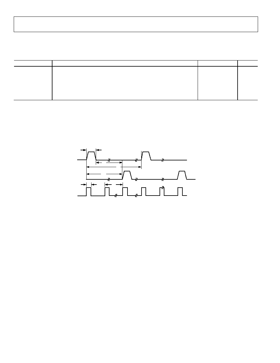
TIMING CHARACTERISTICS
V
DD
= 5 V ± 5%, AGND = DGND = 0 V, on-chip reference, CLKIN = 10 MHz, T
MIN
to T
= 40°C to +85°C, unless otherwise noted
.
1, 2
MAX
Table 2.
Parameter Conditions
Spec
Unit
t
F1 and F2 Pulse Width (Logic High).
275
ms
1
3
t
Output Pulse Period. See the Transfer Function section.
See Table 6. sec
2
t
Time between F1 Falling Edge and F2 Falling Edge.
1/2 t
3
2
sec
t
CF Pulse Width (Logic High).
96
ms
4
3, 4
t
CF Pulse Period. See the Transfer Function and the Frequency Outputs sections.
See Table 7. sec
5
5
t
Minimum Time Between the F1 and F2 Pulse.
CLKIN/4
sec
6
1
Sample tested during initial release and after any redesign or process change that may affect this parameter.
2
See Figure 2.
3
The pulse widths of F1, F2, and CF are not fixed for higher output frequencies. See the Frequency Outputs section.
4
CF is not synchronous to F1 or F2 frequency outputs.
5
The CF pulse is always 1 s in the high frequency mode.
F1
F2
CF
t
1
t
6
t
2
t
3
t
4
t
5
0
267
6-
A
-
00
2
Figure 2. Timing Diagram for Frequency Outputs

ADE7752/ADE7752A
Rev. C | Page 5 of 24
ABSOLUTE MAXIMUM RATINGS
T = 25°C, unless otherwise noted.
A
Table 3.
Parameter Rating
Stresses above those listed under Absolute Maximum Ratings
may cause permanent damage to the device. This is a stress
rating only; functional operation of the device at these or any
other conditions above those listed in the operational sections
of this specification is not implied. Exposure to absolute
maximum rating conditions for extended periods may affect
device reliability.
V to AGND
-0.3 V to +7 V
DD
V to DGND
-0.3 V to +7 V
DD
Analog Input Voltage to AGND
VAP, VBP, VCP, VN, IAP, IAN, IBP, IBN,
ICP, and ICN
-6 V to +6 V
Reference Input Voltage to AGND
-0.3 V to V + 0.3 V
DD
Digital Input Voltage to DGND
-0.3 V to V + 0.3 V
DD
Digital Output Voltage to DGND
-0.3 V to V + 0.3 V
DD
Operating Temperature Range
-40°C to +85°C
Industrial
Storage Temperature Range
-65°C to +150°C
Junction Temperature
150°C
24-Lead SOIC, Power Dissipation
88 mW
JA
Thermal Impedance
250°C/W
Lead Temperature, Soldering
Vapor Phase (60 sec)
215°C
Infrared (15 sec)
220°C
ESD CAUTION
ESD (electrostatic discharge) sensitive device. Electrostatic charges as high as 4000 V readily accumulate on
the human body and test equipment and can discharge without detection. Although this product features
proprietary ESD protection circuitry, permanent damage may occur on devices subjected to high energy
electrostatic discharges. Therefore, proper ESD precautions are recommended to avoid performance
degradation or loss of functionality.
ADE7752/ADE7752A
Rev. C | Page 6 of 24
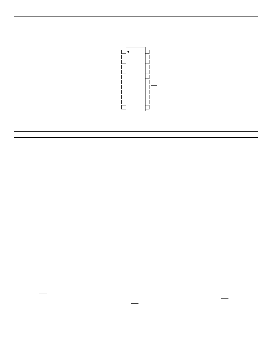
PIN CONFIGURATION AND FUNCTION DESCRIPTIONS
TOP VIEW
(Not to Scale)
ADE7752/
ADE7752A
REF
IN/OUT
AGND
ICN
ICP
IBN
CF
DGND
V
DD
REVP
IBP
IAN
IAP
VN
VCP
VBP
VAP
ABS
S0
F2
S1
F1
SCF
CLKIN
CLKOUT
2
3
4
5
6
7
8
9
10
11
12
1
24
23
22
21
20
19
18
17
16
15
14
13
02
67
6-
A
-
0
03
Figure 3. Pin Configuration
Table 4. Pin Function Descriptions
Pin No.
Mnemonic
Description
1
CF
Calibration Frequency Logic Output. The CF logic output gives instantaneous real power information.
This output is intended to be used for calibration purposes. See the SCF pin description.
2
DGND
This provides the ground reference for the digital circuitry in the ADE7752: the multiplier, filters, and
digital-to-frequency converter. Because the digital return currents in the ADE7752 are small, it is
acceptable to connect this pin to the analog ground plane of the whole system.
3 V
DD
Power Supply. This pin provides the supply voltage for the digital circuitry in the ADE7752. The supply
voltage should be maintained at 5 V ± 5% for specified operation. This pin should be decoupled to
DGND with a 10 F capacitor in parallel with a 100 nF ceramic capacitor.
4
REVP
This logic output goes logic high when negative power is detected on any of the three phase inputs,
that is, when the phase angle between the voltage and the current signals is greater than 90°. This
output is not latched and is reset when positive power is once again detected. See the Negative Power
Information section.
5, 6;
7, 8;
9, 10
IAP, IAN;
IBP, IBN;
ICP, ICN
Analog Inputs for Current Channel. This channel is intended for use with the current transducer and is
referenced in this document as the current channel. These inputs are fully differential voltage inputs
with maximum differential input signal levels of ±0.5 V. See the Analog Inputs section. Both inputs have
internal ESD protection circuitry. In addition, an overvoltage of ±6 V can be sustained on these inputs
without risk of permanent damage.
11
AGND
This pin provides the ground reference for the analog circuitry in the ADE7752: the ADCs, temperature
sensor, and reference. This pin should be tied to the analog ground plane or the quietest ground
reference in the system. This quiet ground reference should be used for all analog circuitry, such as
antialiasing filters, current and voltage transducers, and so on. To keep ground noise around the
ADE7752 to a minimum, the quiet ground plane should connect to the digital ground plane at only
one point. It is acceptable to place the entire device on the analog ground plane.
12 REF
IN/OUT
This pin provides access to the on-chip voltage reference. The on-chip reference has a nominal value of
2.4 V ± 8% and a typical temperature coefficient of 20 ppm/°C. An external reference source may also be
connected at this pin. In either case, this pin should be decoupled to AGND with a 1 F ceramic capacitor.
1316 VN,
VCP,
VBP,
VAP
Analog Inputs for the Voltage Channel. This channel is intended for use with the voltage transducer and
is referenced in this document as the voltage channel. These inputs are single-ended voltage inputs with
a maximum signal level of ±0.5 V with respect to VN for specified operation. All inputs have internal ESD
protection circuitry. In addition, an overvoltage of ± 6 V can be sustained on these inputs without risk of
permanent damage.
17
ABS
This logic input is used to select the way the three active energies from the three phases are summed.
This offers the designer the capability to do the arithmetical sum of the three energies (ABS logic high)
or the sum of the absolute values (ABS logic low). See the Mode Selection of the Sum of the Three Active
Energies section.
18
SCF
Select Calibration Frequency. This logic input is used to select the frequency on the calibration output
CF. Table 7 shows how the calibration frequencies are selected.

ADE7752/ADE7752A
Rev. C | Page 7 of 24
Pin No.
Mnemonic
Description
19
CLKIN
Master Clock for ADCs and Digital Signal Processing. An external clock can be provided at this logic input.
Alternatively, a parallel resonant AT crystal can be connected across CLKIN and CLKOUT to provide a
clock source for the ADE7752. The clock frequency for specified operation is 10 MHz. Ceramic load
capacitors between 22 pF and 33 pF should be used with the gate oscillator circuit. Refer to the crystal
manufacturer's data sheet for load capacitance requirements.
20
CLKOUT
A crystal can be connected across this pin and CLKIN as described previously to provide a clock source
for the ADE7752. The CLKOUT pin can drive one CMOS load when an external clock is supplied at CLKIN
or when a crystal is being used.
21, 22
S0, S1
These logic inputs are used to select one of four possible frequencies for the digital-to-frequency conver-
sion. This offers the designer greater flexibility when designing the energy meter. See the Selecting a
Frequency for an Energy Meter Application section.
24, 23
F1, F2
Low Frequency Logic Outputs. F1 and F2 supply average real power information. The logic outputs can
be used to drive electromechanical counters and two-phase stepper motors directly. See the Transfer
Function section.
ADE7752/ADE7752A
Rev. C | Page 8 of 24
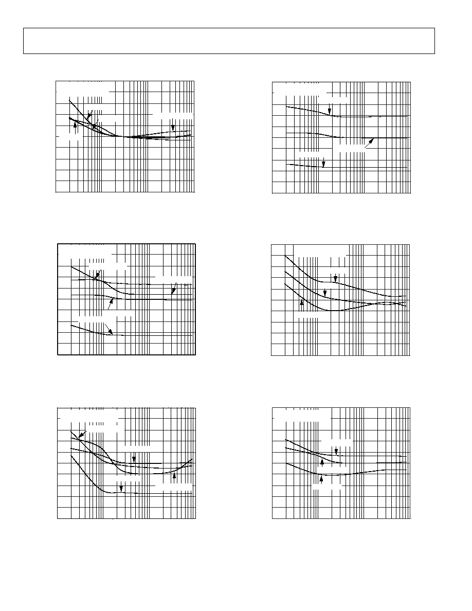
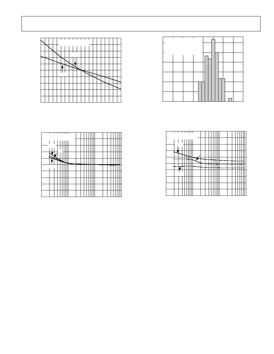
TYPICAL PERFORMANCE CHARACTERISTICS
100
10
CURRENT CHANNEL (% of Full Scale)
0.5
0.1
0.5
0.1
1
0.4
0
0.2
0.4
0.2
0.1
0.3
0.3
E
RROR (% of Re
a
ding)
WYE CONNECTION
ON-CHIP REFERENCE
PHASE C
PHASE B
PHASE A + B + C
PHASE A
02676-A
-
004
100
10
1.0
0.2
1.0
0.1
1
0.8
0
0.4
0.8
0.4
0.2
0.6
0.6
WYE CONNECTION
ON-CHIP REFERENCE
+25
°
C PF = 1
+85
°
C PF = 1
40
°
C PF = 1
CURRENT CHANNEL (% of Full Scale)
E
RROR (% of Re
a
ding)
02676-A
-
007
Figure 4. Error as a Percent of Reading
with Internal Reference (Wye Connection)
Figure 7. Error as a Percent of Reading over Temperature
with Internal Reference (Wye Connection)
100
10
1.0
0.2
1.0
0.1
1
0.8
0
0.4
0.8
0.4
0.2
0.6
0.6
WYE CONNECTION
ON-CHIP REFERENCE
+25
°
C PF = 0.5
+25
°
C PF = +1
+85
°
C PF = +0.5
CURRENT CHANNEL (% of Full Scale)
E
RROR (% of Re
a
ding)
02
67
6-
A
-
00
5
40
°
C PF = +0.5
100
10
0.5
0.1
0.5
0.1
1
0.4
0
0.2
0.4
0.2
0.1
0.3
0.3
DELTA CONNECTION
ON-CHIP REFERENCE
PF = +1
PF = 0.5
PF = +0.5
CURRENT CHANNEL (% of Full Scale)
E
RROR (% of Re
a
ding)
02676-A
-
008
Figure 5. Error as a Percent of Reading over Power Factor
with Internal Reference (Wye Connection)
Figure 8. Error as a Percent of Reading over Power Factor
with Internal Reference (Delta Connection)
100
10
CURRENT CHANNEL (% of Full Scale)
0.5
0.1
0.5
0.1
1
0.4
0
0.2
0.4
0.2
0.1
0.3
0.3
E
RROR (% of Re
a
ding)
WYE CONNECTION
EXTERNAL REFERENCE
+25
°
C PF = 0.5
+25
°
C PF = +1
40
°
C PF = +0.5
+85
°
C PF = +0.5
02676-A
-006
100
10
0.5
0.1
0.1
1
0.4
0
0.2
0.4
0.5
0.2
0.1
0.3
0.3
WYE CONNECTION
EXTERNAL REFERENCE
+25
°
C PF = 1
40
°
C PF = 1
+85
°
C PF = 1
CURRENT CHANNEL (% of Full Scale)
E
RROR (% of Re
a
ding)
02676-A
-
009
Figure 6. Error as a Percent of Reading over Power Factor
with External Reference (Wye Connection)
Figure 9. Error as a Percent of Reading over Temperature
with External Reference (Wye Connection)
ADE7752/ADE7752A
Rev. C | Page 9 of 24
20
15
10
5
5
0
CH_I PhA OFFSET (mV)
18
9
0
20
10
15
12
6
3
15
N: 88
MEAN: 4.48045
SD: 3.23101
MIN: 2.47468 MAX: 12.9385
RANGE: 15.4132
02676-A
-
012
60
65
55
50
FREQUENCY (Hz)
0.5
0.1
0.5
45
0.4
0
0.2
0.4
0.2
0.1
0.3
0.3
PF = 0.5
PF = 1
WYE CONNECTION
ON-CHIP REFERENCE
E
RROR (% of Re
a
ding)
02676-A
-
010
Figure 12. Channel 1 Offset Distribution
Figure 10. Error as a Percent of Reading over Frequency
with an Internal Reference (Wye Connection)
100
10
0.5
0.1
0.5
0.1
1
0.4
0
0.2
0.4
0.2
0.1
0.3
0.3
CURRENT CHANNEL (% of Full Scale)
E
RROR (% of Re
a
ding)
WYE CONNECTION
ON-CHIP REFERENCE
5V
5.25V
4.75V
02676-A
-
013
100
10
0.5
0.1
0.5
0.1
1
0.4
0
0.2
0.4
0.2
0.1
0.3
0.3
WYE CONNECTION
EXTERNAL REFERENCE
5V
5.25V
4.75V
CURRENT CHANNEL (% of Full Scale)
E
RROR (% of Re
a
ding)
02676-A
-
011
Figure 13. Error as a Percent of Reading over Power Supply
with Internal Reference (Wye Connection)
Figure 11. Error as a Percent of Reading over Power Supply
with External Reference (Wye Connection)
ADE7752/ADE7752A
Rev. C | Page 10 of 24
TEST CIRCUIT
V
DD
ABS
REF
IN/OUT
33nF
100nF
33nF
1k
1k
825
1k
10
F
V
DD
VN AGND DGND
F1
3
17
F2
CF
CLKOUT
CLKIN
S0
S1
SCF
10MHz
22pF
22pF
PS2501-1
K7
K8
ADE7752/
ADE7752A
V
DD
1
24
23
TO FREQ.
COUNTER
20
IAP
IAN
IBP
IBN
ICP
ICN
RB
SAME AS
IAP, IAN
SAME AS
IAP, IAN
NOT
CONNECTED
SAME AS VAP
REVP
100nF
10
F
VAP
VBP
VCP
33nF
1k
1M
220V
33nF
1k
SAME AS VAP
5
6
7
8
9
10
16
15
14
13
11
4
12
18
22
21
19
2
I
LOAD
026
76-
A
-
014
Figure 14. Test Circuit for Performance Curves

ADE7752/ADE7752A
Rev. C | Page 11 of 24
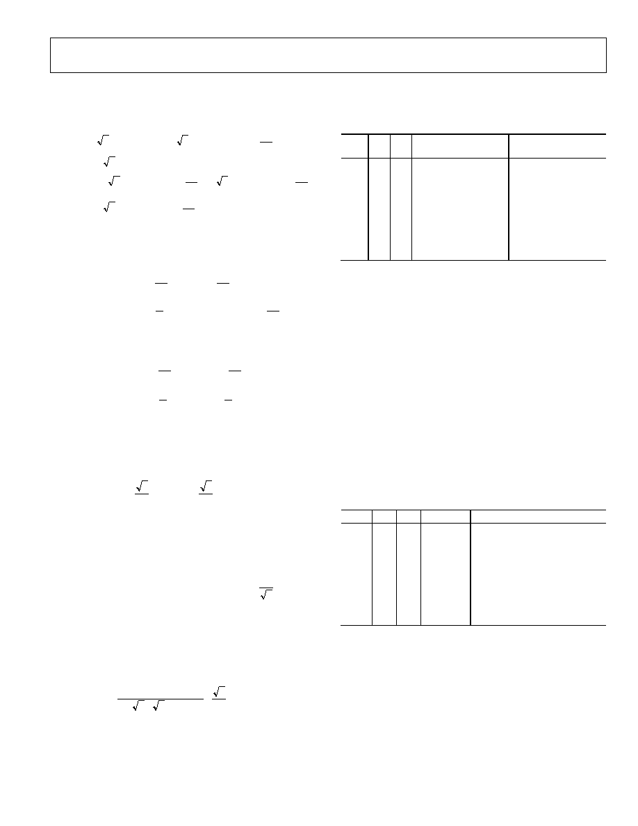
TERMINOLOGY
Measurement Error
The error associated with the energy measurement made by the
ADE7752 is defined by the following formula:
ADC Offset Error
This refers to the dc offset associated with the analog inputs to
the ADCs. It means that with the analog inputs connected to
AGND, the ADCs still see an analog input signal offset.
However, because the HPF is always present, the offset is
removed from the current channel, and the power calculation is
not affected by this offset.
%
Energy
True
Energy
True
ADE
by
Registered
Energy
Error
Percentage
100
7752
×
=
Error Between Channels
The high-pass filter (HPF) in the current channel has a phase
lead response. To offset this phase response and equalize the
phase response between channels, a phase correction network is
also placed in the current channel. The phase correction net-
work ensures a phase match between the current channels and
voltage channels to within ±0.1° over a range of 45 Hz to 65 Hz
and ±0.2° over a range of 40 Hz to 1 kHz. See
Gain Error
The gain error of the ADE7752 is defined as the difference
between the measured output frequency (minus the offset) and
the ideal output frequency. The difference is expressed as a
percentage of the ideal frequency. The ideal frequency is
obtained from the ADE7752 transfer function. See the Transfer
Function
Figure 24 and
section.
Figure 26.
Power Supply Rejection (PSR)
This quantifies the ADE7752 measurement error as a
percentage of reading when the power supplies are varied.
For the ac PSR measurement, a reading at a nominal supply
(5 V) is taken. A 200 mV rms/100 Hz signal is then introduced
onto the supply and a second reading is obtained under the
same input signal levels. Any error introduced is expressed as a
percentage of reading. See definition for Measurement Error.
For the dc PSR measurement, a reading at nominal supplies
(5 V) is taken. The supply is then varied ±5% and a second
reading is obtained with the same input signal levels. Any error
introduced is again expressed as a percentage of reading.
ADE7752/ADE7752A
Rev. C | Page 12 of 24
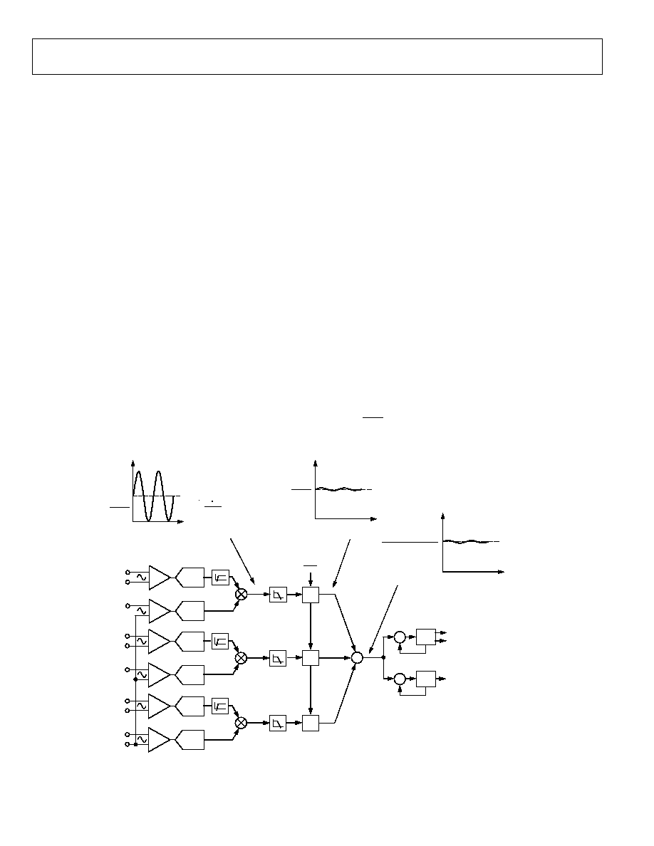
THEORY OF OPERATION
The six voltage signals from the current and voltage transducers
are digitized with ADCs. These ADCs are 16-bit second-order
- with an oversampling rate of 833 kHz. This analog input
structure greatly simplifies transducer interface by providing a
wide dynamic range for direct connection to the transducer and
also by simplifying the antialiasing filter design. A high-pass
filter in the current channel removes the dc component from
the current signal. This eliminates any inaccuracies in the real
power calculation due to offsets in the voltage or current
signals. See the
The low frequency output of the ADE7752 is generated by
accumulating the total real power information. This low
frequency inherently means a long accumulation time between
output pulses. The output frequency is therefore proportional to
the average real power. This average real power information
can, in turn, be accumulated (by a counter, for example) to
generate real energy information. Because of its high output
frequency and therefore shorter integration time, the CF output
is proportional to the instantaneous real power. This pulse is
useful for system calibration purposes that would take place
under steady load conditions.
HPF and Offset Effects section.
The real power calculation is derived from the instantaneous
power signal. The instantaneous power signal is generated by a
direct multiplication of the current and voltage signals of each
phase. In order to extract the real power component (the dc
component), the instantaneous power signal is low-pass filtered
on each phase.
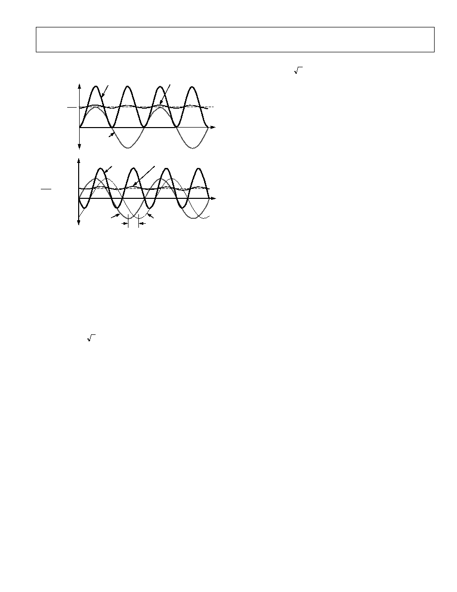
POWER FACTOR CONSIDERATIONS
Low-pass filtering, the method used to extract the real power
information from the individual instantaneous power signal, is
still valid when the voltage and current signals of each phase are
not in phase.
Figure 15 illustrates the instantaneous real
power signal and shows how the real power information can be
extracted by low-pass filtering the instantaneous power signal.
This method is used to extract the real power information on
each phase of the polyphase system. The total real power
information is then obtained by adding the individual phase
real power. This scheme correctly calculates real power for
nonsinusoidal current and voltage waveforms at all power
factors. All signal processing is carried out in the digital domain
for superior stability over temperature and time.
Figure 16 displays the unity power factor
condition and a DPF (displacement power factor) = 0.5, or
current signal lagging the voltage by 60°, for one phase of the
polyphase. Assuming that the voltage and current waveforms
are sinusoidal, the real power component of the instantaneous
power signal, or the dc term, is given by
( )
°
×
×
60
cos
2
1
V
TIME
IAP
IAN
VAP
HPF
LPF
IBP
IBN
VBP
ICP
ICN
VCP
VN
DIGITAL-TO-
FREQUENCY
DIGITAL-TO-
FREQUENCY
F1
F2
CF
INSTANTANEOUS
REAL POWER SIGNAL
INSTANTANEOUS
POWER SIGNAL - p(t)
INSTANTANEOUS
TOTAL
POWER SIGNAL
VA
×
IA + VB
×
IB +
VC
×
IC
2
ABS
|X|
LPF
LPF
|X|
|X|
p(t) = i(t)
×
v(t)
WHERE:
V
×
I
2
{1+ cos (2
t)}
v(t) = V
×
cos (
t)
i(t) = I
×
cos (
t)
p(t) =
V
×
I
2
V
×
I
V
×
I
2
MULTIPLIER
MULTIPLIER
MULTIPLIER
HPF
HPF
ADC
ADC
ADC
ADC
ADC
ADC
0
2676
-
A
-
015
Figure 15. Signal Processing Block Diagram
ADE7752/ADE7752A
Rev. C | Page 13 of 24
This is the correct real power calculation.
( )
(
n
n
n
O
t
n
I
V
I
t
i
sin
2
0
×
×
+
=
=
)
(2)
INSTANTANEOUS
REAL POWER SIGNAL
INSTANTANEOUS
POWER SIGNAL
V
×
I
2
×
cos(60
°
)
V
×
I
2
INSTANTANEOUS
POWER SIGNAL
INSTANTANEOUS REAL
POWER SIGNAL
60
°
CURRENT
CURRENT
VOLTAGE
0V
0V
VOLTAGE
02676-
A-
016
where:
i(t) is the instantaneous current.
I
O
is the dc component.
I
n
is the rms value of current harmonic n.
is the phase angle of the current harmonic.
n
Using Equations 1 and 2, the real power, P, can be expressed in
terms of its fundamental real power (P
1
) and harmonic real
power (P
H
).
+ P
P = P
1
H
where:
1
1
1
1
1
1
1
I
V
P
-
=
×
=
cos
(3)
Figure 16. DC Component of Instantaneous Power Signal
Conveys Real Power Information PF < 1
n
n
n
n
n
n
H
n
I
V
P
-
=
×
=
=
cos
1
(4)
NONSINUSOIDAL VOLTAGE AND CURRENT
The real power calculation method also holds true for nonsin-
usoidal current and voltage waveforms. All voltage and current
waveforms in practical applications have some harmonic
content. Using the Fourier Transform, instantaneous voltage
and current waveforms can be expressed in terms of their
harmonic content:
( )
(
n
n
n
o
t
n
V
V
t
v
+
×
×
+
=
=
sin
2
0
)
(1)
As can be seen from Equation 4, a harmonic real power compo-
nent is generated for every harmonic, provided that harmonic is
present in both the voltage and current waveforms. The power
factor calculation has been shown to be accurate in the case of a
pure sinusoid. Therefore, the harmonic real power must also
correctly account for power factor since it is made up of a series
of pure sinusoids.
Note that the input bandwidth of the analog inputs is 14 kHz
with a master clock frequency of 10 MHz.
where:
v(t) is the instantaneous voltage.
V
O
is the average value.
V
n
is the rms value of voltage harmonic n.
n
is the phase angle of the voltage harmonic.
ADE7752/ADE7752A
Rev. C | Page 14 of 24
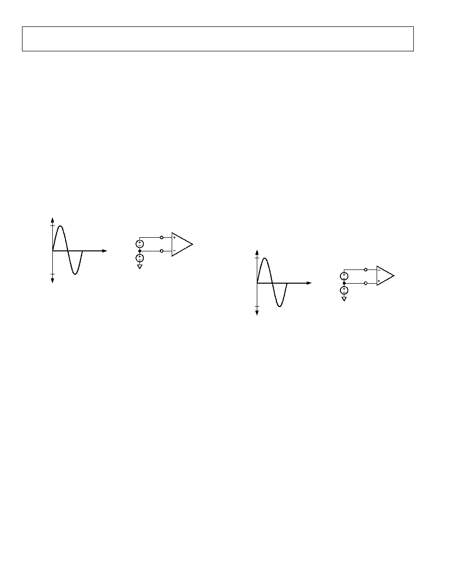
ANALOG INPUTS
CURRENT CHANNELS
VOLTAGE CHANNELS
The voltage outputs from the current transducers are connected
to the ADE7752 current channels, which are fully differential
voltage inputs. IAP, IBP, and ICP are the positive inputs for IAN,
IBN, and ICN, respectively.
The output of the line voltage transducer is connected to the
ADE7752 at this analog input. Voltage channels are a pseudo-
differential voltage input. VAP, VBP, and VCP are the positive
inputs with respect to VN.
The maximum peak differential signal on the current channel
should be less than ±500 mV (353 mV rms for a pure sinusoidal
signal) for the specified operation.
The maximum peak differential signal on the voltage channel
is ±500 mV (353 mV rms for a pure sinusoidal signal) for
specified operation.
Figure 17 illustrates the maximum signal levels on IAP and
IAN. The maximum differential voltage between IAP and IAN
is ±500 mV. The differential voltage signal on the inputs must
be referenced to a common mode, such as AGND. The maxi-
mum common-mode signal shown in
Figure 18 illustrates the maximum signal levels that can be
connected to the voltage channels of the ADE7752.
Voltage channels must be driven from a common-mode voltage.
In other words, the differential voltage signal on the input must
be referenced to a common mode (usually AGND). The analog
inputs of the ADE7752 can be driven with common-mode
voltages of up to 25 mV with respect to AGND. However, best
results are achieved using a common mode equal to AGND.
Figure 17 is ±25 mV.
DIFFERENTIAL INPUT
±
500mV MAX PEAK
+500mV
AGND
V
CM
IA
IAP
V
CM
500mV
COMMON-MODE
±
25mV MAX
IAN
IAPIAN
02676-A
-
017
DIFFERENTIAL INPUT
±
500mV MAX PEAK
+500mV
AGND
VCM
VA
VAP
V
CM
500mV
COMMON-MODE
±
25mV MAX
VN
VAPVN
02676-A
-
018
Figure 17. Maximum Signal Levels, Current Channel
Figure 18. Maximum Signal Levels, Voltage Channel
ADE7752/ADE7752A
Rev. C | Page 15 of 24
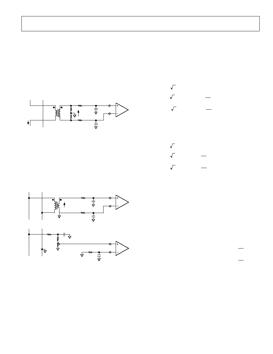
TYPICAL CONNECTION DIAGRAMS
CURRENT CHANNEL CONNECTION
METER CONNECTIONS
Figure 19 shows a typical connection diagram for the current
channel (IA). A current transformer (CT) is the current trans-
ducer selected for this example. Notice the common-mode
voltage for the current channel is AGND and is derived by
center tapping the burden resistor to AGND. This provides the
complementary analog input signals for IAP and IAN. The CT
turns ratio and burden resistor Rb are selected to give a peak
differential voltage of ±500 mV at maximum load.
In 3-phase service, two main power distribution services exist:
3-phase 4-wire or 3-phase 3-wire. The additional wire in the
3-phase 4-wire arrangement is the neutral wire. The voltage
lines have a phase difference of ±120° (±2/3 radians) between
each other. See Equation 5.
( )
( )
( )
( )
+
×
×
=
+
×
×
=
×
×
=
3
4
cos
2
3
2
cos
2
cos
2
t
V
t
V
t
V
t
V
t
V
t
V
l
C
C
l
B
B
l
A
A
(5)
IAP
±
500mV
R
b
Rf
Rf
CT
NEUTRAL
PHASE
IP
IAN
Cf
Cf
02676-
A
-
01
9
where V
Figure 19. Typical Connection for Current Channels
VOLTAGE CHANNELS CONNECTION
Figure 20 shows two typical connections for the voltage
channel. The first option uses a potential transformer (PT) to
provide complete isolation from the main voltage. In the second
option, the ADE7752 is biased around the neutral wire, and a
resistor divider is used to provide a voltage signal proportional
to the line voltage. Adjusting the ratio of Ra, Rb, and VR is also
a convenient way of carrying out a gain calibration on the meter.
±
500mV
Ra
*
Rb
*
VR
*
VAP
AGND
Rf
Rf
PT
NEUTRAL
PHASE
VN
Cf
Cf
VAP
Rf
NEUTRAL
PHASE
VN
Cf
Cf
*
Ra >> Rf + VR;
*
Rb + VR = Rf
02676-A
-
018
±
500mV
Figure 20. Typical Connections for Voltage Channels
A
, V
B
, and V
C
B
represent the voltage rms values of the
different phases.
The current inputs are represented by Equation 6.
( )
(
)
( )
( )
+
+
×
=
+
+
×
=
+
×
=
C
l
C
C
B
l
B
B
A
l
A
A
t
I
t
I
t
I
t
I
t
I
t
I
3
4
cos
2
3
2
cos
2
cos
2
(6)
where I
A
, I
B
, and I
C
B
represent the rms value of the current of
each phase and
A
,
B
B
, and
C
represent the phase difference of
the current and voltage channel of each phase.
The instantaneous powers can then be calculated as follows:
P
A
(t) = V
A
(t) × I
A
(t)
P
B
(t) = V
B
B
(t) × I
B
B
(t)
P
B
C
(t) = V
C
(t) × I
C
(t)
Then:
( )
( )
(
)
( )
( )
( )
( )
+
+
×
×
-
×
×
=
+
+
×
×
-
×
×
=
+
×
×
-
×
×
=
C
l
C
C
C
C
C
C
B
l
B
B
B
B
B
B
A
l
A
A
A
A
A
A
t
I
V
I
V
t
P
t
I
V
I
V
t
P
t
I
V
I
V
t
P
3
8
2
cos
cos
3
4
2
cos
cos
2
cos
cos
(7)
As shown in Equation 7, in the ADE7752, the real power calcu-
lation per phase is made when current and voltage inputs of one
phase are connected to the same channel (A, B, or C). Then the
summation of each individual real power calculation gives the
total real power information, P(t) = P
A
(t) + P
B
(t) + P
C
(t).
B
ADE7752/ADE7752A
Rev. C | Page 16 of 24
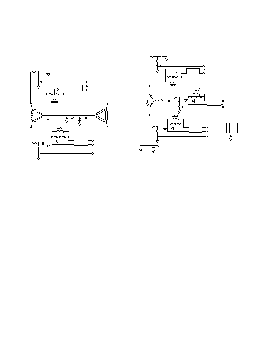
Figure 21 shows the connections of the analog inputs of the
ADE7752 with the power lines in a 3-phase 3-wire delta service.
Note that only two current inputs and two voltage inputs of the
ADE7752 are used in this case. The real power calculated by the
ADE7752 does not depend on the selected channels.
Figure 22 shows the connections of the analog inputs of the
ADE7752 with the power lines in a 3-phase 4-wire Wye service.
SOURCE
ICP
ICN
LOAD
CT
IBP
IBN
ANTIALIASING
FILTERS
PHASE A
PHASE B
PHASE C
Rb*
Ra*
VR*
Cf
VAP
CT
Rb*
ANTIALIASING
FILTERS
IAP
IAN
CT
Rb*
ANTIALIASING
FILTERS
Rb*
Ra*
VR*
Cf
VCP
Rf
CF
VN
Rb*
Ra*
VR*
Cf
VBP
Rb*
*
Ra >> Rf + VR;
*
Rb + VR = Rf
02676-A
-
022
CT
Rb*
ANTIALIASING
FILTERS
IAP
IAN
SOURCE
Rb*
Ra*
Rb*
VR*
Rf
Cf
Cf
VN
Ra*
VR*
Cf
LOAD
PHASE A
PHASE B
PHASE C
CT
Rb*
VAP
VBP
ANTIALIASING
FILTERS
IBN
IBP
*
Ra >> Rf + VR
*
Rb + VR = Rf
02
676
-
A
-
021
Figure 22. 3-Phase 4-Wire Meter Connection with ADE7752
Figure 21. 3-Phase 3-Wire Meter Connection with ADE7752
ADE7752/ADE7752A
Rev. C | Page 17 of 24
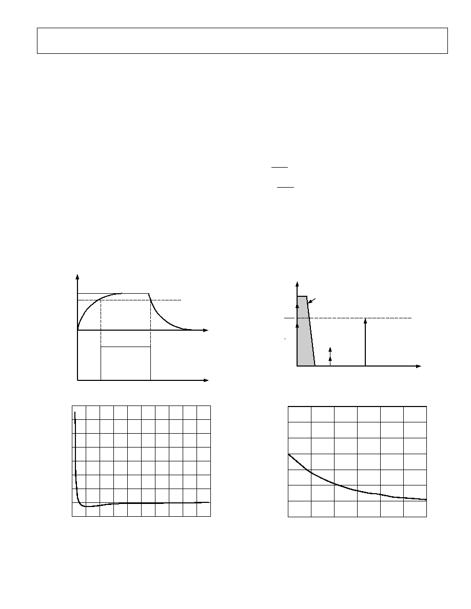
POWER SUPPLY MONITOR
The ADE7752 contains an on-chip power supply monitor. The
power supply (V
DD
) is continuously monitored by the ADE7752.
If the supply is less than 4 V ± 5%, the outputs of the ADE7752
are inactive. This is useful to ensure correct device startup at
power-up and power-down. The power supply monitor has
built-in hysteresis and filtering. This gives a high degree of
immunity to false triggering due to noisy supplies.
As can be seen from Figure 23, the trigger level is nominally set
at 4 V. The tolerance on this trigger level is about ±5%. The
power supply and decoupling for the part should be such that
the ripple at V
DD
does not exceed 5 V ± 5% as specified for
normal operation.
HPF AND OFFSET EFFECTS
Figure 25 shows the effect of offsets on the real power calcula-
tion. As can be seen, an offset on the current channel and
voltage channel contribute a dc component after multiplication.
Since this dc component is extracted by the LPF and is used to
generate the real power information for each phase, the offsets
contribute a constant error to the total real power calculation.
This problem is easily avoided by the HPF in the current
channels. By removing the offset from at least one channel, no
error component can be generated at dc by the multiplication.
Error terms at cos(t) are removed by the LPF and the digital-
to-frequency conversion. See the Digital-to-Frequency
Conversion section.
( )
{
}
( )
{
}
( )
( )
(
)
t
I
V
t
V
I
t
I
V
I
V
I
V
I
t
I
V
t
V
OS
OS
OS
OS
OS
OS
2
cos
2
cos
cos
2
cos
cos
×
×
+
×
+
×
+
×
+
×
=
+
×
+
The HPFs in the current channels have an associated phase
response that is compensated for on-chip. Figure 24 and
Figure 26 show the phase error between channels with the
compensation network. The ADE7752 is phase compensated
up to 1 kHz as shown. This ensures correct active harmonic
power calculation even at low power factors.
V
DD
5V
4V
0V
INTERNAL
RESET
INACTIVE
TIME
ACTIVE
INACTIVE
02676-A
-
023
V
OS
×
I
OS
I
OS
×
V
V
OS
×
I
DC COMPONENT (INCLUDING ERROR TERM)
IS EXTRACTED BY THE LPF FOR REAL
POWER CALCULATION
2
FREQUENCY RAD/S
2
V
×
I
0
02676-A
-
024
Figure 23. On-Chip Power Supply Monitor
Figure 25. Effect of Channel Offset on the Real Power Calculation
FREQUENCY (Hz)
0.07
0.06
0.01
0
1000
200
400
600
800
PH
A
SE (
D
egrees)
0.03
0.02
0.01
0
0.05
0.04
100
300
500
700
900
02676-A
-
025
FREQUENCY (Hz)
0.010
0.008
0.004
40
70
45
50
PH
A
SE (
D
egrees)
0.002
0
0.002
0.006
0.004
55
60
65
02676-A
-
026
Figure 24. Phase Error Between Channels (0 Hz to 1 kHz)
Figure 26. Phase Error Between Channels (40 Hz to 70 Hz)
ADE7752/ADE7752A
Rev. C | Page 18 of 24
DIGITAL-TO-FREQUENCY CONVERSION
After multiplication, the digital output of the low-pass filter
contains the real power information of each phase. Because this
LPF is not an ideal brick wall filter implementation, however,
the output signal also contains attenuated components at the
line frequency and its harmonics (cos(ht), where h = 1, 2, 3,
and so on).
power signal. The average value of a sinusoidal signal is zero.
Thus, the frequency generated by the ADE7752 is proportional
to the average real power. Figure 27 shows the digital-to-
frequency conversion for steady load conditions, constant
voltage, and current.
Figure 27
As can be seen in
The magnitude response of the filter is given by
( )
2
8
1
1
|
|
+
=
f
f
H
(8)
, the frequency output CF varies
over time, even under steady load conditions. This frequency
variation is primarily due to the cos(2t) components in the
instantaneous real power signal. The output frequency on CF
can be up to 160 times higher than the frequency on F1 and F2.
The higher output frequency is generated by accumulating the
instantaneous real power signal over a much shorter time, while
converting it to a frequency. This shorter accumulation period
means less averaging of the cos(2t) component. As a conse-
quence, some of this instantaneous power signal passes through
the digital-to-frequency conversion. This is not a problem in
the application. Where CF is used for calibration purposes, the
frequency should be averaged by the frequency counter. This
removes any ripple. If CF is being used to measure energy, such
as in a microprocessor-based application, the CF output should
also be averaged to calculate power. Because the outputs F1 and
F2 operate at a much lower frequency, much more averaging of
the instantaneous real power signal is carried out. The result is a
greatly attenuated sinusoidal content and a virtually ripple-free
frequency output.
where the -3 dB cutoff frequency of the low-pass filter is 8 Hz.
For a line frequency of 50 Hz, this would give an attenuation of
the 2(100 Hz) component of approximately 22 dB. The
dominating harmonic is twice the line frequency, cos(2t), due
to the instantaneous power signal. Figure 27 shows the
instantaneous real power signal at the output of the CF, which
still contains a significant amount of instantaneous power
information, cos (2t).
This signal is then passed to the digital-to-frequency converter
where it is integrated (accumulated) over time to produce an
output frequency. This accumulation of the signal suppresses or
averages out any non-dc component in the instantaneous real
LPF TO EXTRACT
REAL POWER
(DC TERM)
MULTIPLIER
LPF
MULTIPLIER
LPF
MULTIPLIER
LPF
DIGITAL-TO-
FREQUENCY
DIGITAL-TO-
FREQUENCY
F1
F2
CF
VA
IA
VB
IB
VC
IC
FRE
Q
UE
NCY
CF
FRE
Q
UE
NCY
TIME
F1
cos(2
t)
ATTENUATED BY LPF
2
FREQUENCY RAD/S
2
V
×
I
0
INSTANTANEOUS REAL POWER SIGNAL
(FREQUENCY DOMAIN)
|X|
|X|
|X|
ABS
TIME
02676-A
-
027
Figure 27. Real Power-to-Frequency Conversion

ADE7752/ADE7752A
Rev. C | Page 19 of 24
MODE SELECTION OF THE SUM OF THE THREE
ACTIVE ENERGIES
The ADE7752 can be configured to execute the arithmetic sum
of the three active energies, Wh = Wh
A
+ Wh
B
+ Wh
C
, or the
sum of the absolute value of these energies, Wh = |Wh
A
| +
|Wh
B
| + |Wh
C
|. The selection between the two modes can be
made by setting the ABS pin. Logic high and logic low applied
on the ABS pin correspond to the arithmetic sum and the sum
of absolute values, respectively.
When the sum of the absolute values is selected, the active
energy from each phase is always counted positive in the total
active energy. It is particularly useful in 3-phase 4-wire installa-
tion where the sign of the active power should always be the
same. If the meter is misconnected to the power lines, (for
instance, if CT is connected in the wrong direction), the total
active energy recorded without this solution can be reduced by
two-thirds.
The sum of the absolute values assures that the active energy
recorded represents the actual active energy delivered. In this
mode, the reverse power pin still detects when negative power is
present on any of the three phase inputs.
POWER MEASUREMENT CONSIDERATIONS
Calculating and displaying power information always has some
associated ripple that depends on the integration period used in
the MCU to determine average power as well as the load. For
example, at light loads, the output frequency may be 10 Hz.
With an integration period of 2 seconds, only about 20 pulses
are counted. The possibility of missing one pulse always exists
since the ADE7752 output frequency is running asynchro-
nously to the MCU timer. This would result in a 1-in-20 or
5% error in the power measurement.
ADE7752/ADE7752A
Rev. C | Page 20 of 24
TRANSFER FUNCTION
FREQUENCY OUTPUTS F1 AND F2
F
17
= 0.60 Hz, SCF = S0 = S1 = 1
V
The ADE7752 calculates the product of six voltage signals (on
current channel and voltage channel) and then low-pass filters
this product to extract real power information. This real power
information is then converted to a frequency. The frequency
information is output on F1 and F2 in the form of active high
pulses. The pulse rate at these outputs is relatively low, such as
29.32 Hz maximum for ac signals with SCF = 1; S0 = S1 = 1 (see
Table 6). This means that the frequency at these outputs is
generated from real power information accumulated over a
relatively long period of time. The result is an output frequency
that is proportional to the average real power. The averaging of
the real power signal is implicit to the digital-to-frequency
conversion. The output frequency or pulse rate is related to the
input voltage signals by the following equation:
(
)
2
7
1
181
.
6
REF
C
CN
B
BN
A
AN
V
F
I
V
I
V
I
V
Freq
-
×
×
+
×
+
×
×
=
where:
Freq = the output frequency on F1 and F2 (Hz).
V
AN,
V
BN,
and V
CN
= the differential rms voltage signal on voltage
channels (V).
I
A,
I
B,
and I
C
= the differential rms voltage signal on current
channels (V).
V
REF
= the reference voltage (2.4 V ± 8%) (V).
F
17
= one of seven possible frequencies selected by using the
logic inputs SCF, S0, and S1 (see Table 5).
Table 5. F
17
Frequency Selection
1
SCF
S1
S0
F
17
(Hz)
0 0
0
1.27
1 0
0
1.19
0 0
1
5.09
1 0
1
4.77
0 1
0
19.07
1 1
0
19.07
0 1
1
76.29
1 1
1
0.60
1
F
17
is a fraction of the master clock and therefore varies if the specified
CLKIN frequency is altered.
Example 1
Thus, if full-scale differential dc voltages of +500 mV are
applied to VA, VB, VC, IA, IB, and IC, respectively (500 mV is
the maximum differential voltage that can be connected to
current and voltage channels), the expected output frequency is
calculated as follows:
AN
= V = V
BN
CN
= IA = IB = IC = 500 mV dc =
0.5 V(rms of dc = dc)
V
REF
= 2.4 V (nominal reference value)
Note that if the on-chip reference is used, actual output fre-
quencies may vary from device to device due to reference
tolerance of ±8%.
Hz
483
.
0
4
.
2
60
.
0
5
.
0
5
.
0
181
.
6
3
2
=
×
×
×
×
=
Freq
Example 2
In this example, with ac voltages of ±500 mV peak applied to
the voltage channels and current channels, the expected output
frequency is calculated as follows:
(
)
value
reference
nominal
V
AC
IC
IB
IA
V
V
V
S
S
SCF
F
REF
CN
BN
AN
V
4
.
2
Vrms
2
5
.
0
peak
mV
500
1
1
0
,
Hz
60
.
0
7
1
=
=
=
=
=
=
=
=
=
=
=
=
-
Note that if the on-chip reference is used, actual output fre-
quencies may vary from device to device due to reference
tolerance of ±8%.
Hz
24
.
0
4
.
2
2
2
6
.
0
5
.
0
5
.
0
181
.
6
3
2
=
×
×
×
×
×
×
=
Freq
As can be seen from these two example calculations, the
maximum output frequency for ac inputs is always half of that
for dc input signals. The maximum frequency also depends on
the number of phases connected to the ADE7752. In a 3-phase
3-wire delta service, the maximum output frequency is different
from the maximum output frequency in a 3-phase
4-wire Wye service. The reason is that there are only two phases
connected to the analog inputs, but also that in a delta service,
the current channel input and voltage channel input of the same
phase are not in phase in normal operation.
Example 3
In this example, the ADE7752 is connected to a 3-phase 3-wire
delta service as shown in Figure 21. The total real energy
calculation processed in the ADE7752 can be expressed as
Total Real Power = (V
A
- V
C
) × I
A
+ (V
B
- V
C
) × I
B
B
B
where V
A
, V
B
, and V
C
B
represent the voltage on Phase A, B, and
C, respectively. I
A
and I
B
B
represent the current on Phase A and
B, respectively.
ADE7752/ADE7752A
Rev. C | Page 21 of 24
Table 6 shows a complete listing of all maximum output
frequencies when using all three channel inputs.
As the voltage and current inputs respect Equations 5 and 6, the
total real power (P) is
(
) (
) (
) (
)
( )
( )
+
×
×
×
+
×
×
-
+
×
×
+
×
×
×
+
×
×
-
×
×
=
-
×
-
+
-
-
=
3
2
cos
2
3
4
cos
2
3
2
cos
2
cos
2
3
4
cos
2
cos
2
t
I
t
V
v
t
V
t
I
t
V
t
V
P
I
I
V
V
I
I
V
V
P
l
B
l
C
l
B
l
A
l
C
l
A
BN
BP
C
B
AN
AP
C
A
Table 6. Maximum Output Frequency on F1 and F2
For simplification, assume that
A
=
B
=
B
C
= 0 and
V
A
= V
B
B
= V
C
= V. The preceding equation becomes:
( )
(
)
+
×
+
×
×
×
×
+
×
+
×
×
×
×
=
3
2
cos
sin
3
sin
2
cos
3
2
sin
3
2
sin
2
t
t
I
V
t
t
I
V
P
l
l
B
l
l
A
(9)
P then becomes:
+
+
×
×
+
+
+
×
×
=
3
2
sin
3
sin
3
2
2
sin
3
2
sin
t
I
V
t
I
V
P
l
B
BN
l
A
AN
(10)
where V
AN
= V × sin(2/3) and V
BN
= V × sin(/3).
As the LPF on each channel eliminates the 2l component of
the equation, the real power measured by the ADE7752 is
2
3
2
3
×
×
+
×
×
=
B
BN
A
AN
I
V
I
V
P
If full-scale ac voltage of ±500 mV peak is applied to the voltage
channels and current channels, the expected output frequency
is calculated as follows:
value
reference
nominal
V
4
.
2
0
2
5
.
0
500
1
1
0
,
60
.
0
7
1
=
=
=
=
=
=
=
=
=
=
=
=
=
-
REF
C
CN
C
B
A
BN
AN
V
I
V
rms
ac
peak
I
I
I
V
V
S
S
SCF
F
V
V
m
Hz
Note that if the on-chip reference is used, actual output fre-
quencies may vary from device to device due to reference
tolerance of ±8%.
Hz
139
.
0
2
3
4
.
2
2
2
60
.
0
5
.
0
5
.
0
181
.
6
2
2
=
×
×
×
×
×
×
×
=
Freq
SCF S1 S0
Max Frequency for
AC Inputs (Hz)
Max Frequency for
DC Inputs (Hz)
1.02
0 0 0 0.51
1 0 0 0.48
0.96
0 0 1 2.04
4.09
1 0 1 1.91
3.84
0 1 0 7.67
15.35
1 1 0 7.67
15.35
0 1 1 30.70
61.4
0.48
1 1 1 0.24
FREQUENCY OUTPUT CF
The pulse output calibration frequency (CF) is intended for use
during calibration. The output pulse rate on CF can be up to
160 times the pulse rate on F1 and F2. The lower the F
17
frequency selected, the higher the CF scaling. Table 7 shows
how the two frequencies are related, depending on the states of
the logic inputs S0, S1, and SCF. Because of its relatively high
pulse rate, the frequency at this logic output is proportional to
the instantaneous real power. As with F1 and F2, the frequency
is derived from the output of the low-pass filter after multiplica-
tion. However, because the output frequency is high, this real
power information is accumulated over a much shorter time.
Thus, less averaging is carried out in the digital-to-frequency
conversion. With much less averaging of the real power signal,
the CF output is much more responsive to power fluctuations.
See Figure 15.
Table 7. Maximum Output Frequency on CF
SCF S1 S0 F
17
(Hz)
CF Max for AC Signals (Hz)
0
0
0
1.27
160 × F1, F2 = 81.87
1
0
0
1.19
8 × F1, F2 = 3.83
0
0
1
5.09
160 × F1, F2 = 327.46
1
0
1
4.77
16 × F1, F2 = 30.70
0
1
0
19.07
16 × F1, F2 = 122.81
1
1
0
19.07
8 × F1, F2 = 61.40
0
1
1
76.29
8 × F1, F2 = 245.61
1
1
1
0.60
16 × F1, F2 = 3.84

ADE7752/ADE7752A
Rev. C | Page 22 of 24
SELECTING A FREQUENCY FOR AN ENERGY METER APPLICATION
As shown in Table 5, the user can select one of seven frequen-
cies. This frequency selection determines the maximum
frequency on F1 and F2. These outputs are intended to be
used to drive the energy register (electromechanical or other).
Since only seven different output frequencies can be selected,
the available frequency selection has been optimized for a 3-
phase 4-wire service with a meter constant of 100 imp/kWhr
and a maximum current between 10 A and 100 A. Table 8
shows the output frequency for several maximum currents
(I
MAX
) with a line voltage of 220 V (phase neutral). In all cases,
the meter constant is 100 imp/kWhr.
Table 8. V. F1 and F2 Frequency at 100 imp/kWhr
I
MAX
(A)
F1 and F2 (Hz)
10 0.18
25 0.46
40 0.73
60 1.10
80 1.47
100 1.83
The F
17
frequencies allow complete coverage of this range of
output frequencies on F1 and F2. When designing an energy
meter, the nominal design voltage on the voltage channels
should be set to half scale to allow for calibration of the meter
constant. The current channel should also be no more than
half scale when the meter sees maximum load. This allows
overcurrent signals and signals with high crest factors to be
accommodated. Table 9 shows the output frequency on F1 and
F2 when all six analog inputs are half scale.
Table 9. F1 and F2 Frequency with Half-Scale AC Inputs
SCF S1 S0 F
17
Frequency on F1 and F2
(Half-Scale AC Inputs)
0 0
0
1.27
0.26
1 0
0
1.19
0.24
0 0
1
5.09
1.02
1 0
1
4.77
0.96
0 1
0
19.07
3.84
1 1
0
19.07
3.84
0 1
1
76.29
15.35
1 1
1
0.60
0.12
When selecting a suitable F
17
frequency for a meter design, the
frequency output at I
MAX
(maximum load) with a 100 imp/kWhr
meter constant should be compared with column 5 of Table 9.
The frequency closest to that listed in Table 9 is the best choice
of frequency (F
17
). For example, if a 3-phase 4-wire Wye meter
with a 25 A maximum current is being designed, the output
frequency on F1 and F2 with a 100 imp/kWhr meter constant is
0.15 Hz at 25 A and 220 V (from Table 8). Looking at Table 9,
the closest frequency to 0.15 Hz in column 5 is 0.12 Hz.
Therefore, F
17
= 0.6 Hz is selected for this design.
FREQUENCY OUTPUTS
Figure 2 shows a timing diagram for the various frequency
outputs. The outputs F1 and F2 are the low frequency outputs
that can be used to directly drive a stepper motor or electro-
mechanical impulse counter. The F1 and F2 outputs provide
two alternating high going pulses. The pulse width (t
1
) is set at
275 ms, and the time between the rising edges of F1 and F2 (t
3
)
is approximately half the period of F1 (t
2
). If, however, the
period of F1 and F2 falls below 550 ms (1.81 Hz), the pulse
width of F1 and F2 is set to half of their period. The maximum
output frequencies for F1 and F2 are shown in Table 6.
The high frequency CF output is intended to be used for
communications and calibration purposes. CF produces a
96 ms-wide active high pulse (t
4
) at a frequency proportional to
active power. The CF output frequencies are given in Table 7. As
in the case of F1 and F2, if the period of CF (t
5
) falls below
192 ms, the CF pulse width is set to half the period. For
example, if the CF frequency is 20 Hz, the CF pulse width is
25 ms. One exception to this is when the mode is S0 = 1,
SCF = S1 = 0. In this case, the CF pulse width is 66% of the period.
NO LOAD THRESHOLD
The ADE7752 also includes no load threshold and start-up cur-
rent features that eliminate any creep effects in the meter. The
ADE7752 is designed to issue a minimum output frequency.
Any load generating a frequency lower than this minimum fre-
quency does not cause a pulse to be issued on F1, F2, or CF. The
minimum output frequency is given as 0.005% of the full-scale
output frequency for each of the F
17
frequency selections or
approximately 0.00204% of the F
17
frequency (see Table 10).
For example, for an energy meter with a 100 imp/kWhr meter
constant using F
17
(4.77 Hz), the minimum output frequency at
F1 or F2 would be 9.59 × 10
5
Hz. This would be 1. 54× 10
3
Hz
at CF (16 × F1 Hz). In this example, the no load threshold
would be equivalent to 3.45 W of load or a start-up current of
15.70 mA at 240 V.
Table 10. CF, F1, and F2 Minimum Frequency at No Load
Threshold
SCF
S1
S0
F1, F2 Min (Hz)
CF Min (Hz)
0
0
0
2.56 x 10
-05
4.09 x 10
-03
1
0
0
2.40 x 10
-05
1.92 x 10
-04
0
0
1
1.02 x 10
-04
1.64 x 10
-02
1
0
1
9.59 x 10
-05
1.54 x 10
-03
0
1
0
3.84 x 10
-04
6.14 x 10
-03
1
1
0
3.84 x 10
-04
3.07 x 10
-03
0
1
1
1.54 x 10
-03
1.23 x 10
-02
1
1
1
1.20 x 10
-05
1.92 x 10
-04

ADE7752/ADE7752A
Rev. C | Page 23 of 24
NEGATIVE POWER INFORMATION
The ADE7752 detects when the current and voltage channels of
any of the three phase inputs have a phase difference greater
than 90°:
A
or
B
or
B
C
> 90°. This mechanism can detect
wrong connection of the meter or generation of active energy.
The REVP pin output goes active high when negative power is
detected on any of the three phase inputs. If positive active
energy is detected on all the three phases, REVP pin output is low.
The REVP pin output changes state at the same time a pulse is
issued on CF. If several phases measure negative power, the
REVP pin output stays high until all the phases measure
positive power. If a phase has gone below the no load threshold,
REVP detection on this phase is disabled. REVP detection on
this phase resumes when the power returns out of no load
condition. See the No Load Threshold section.
ADE7752/ADE7752A
Rev. C | Page 24 of 24
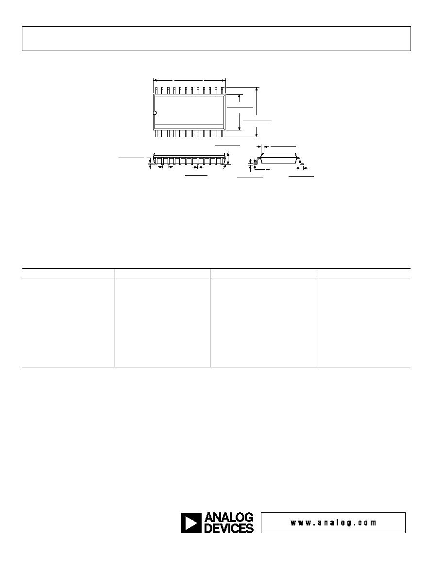
OUTLINE DIMENSIONS
COMPLIANT TO JEDEC STANDARDS MS-013-AD
8°
0°
0.75 (0.0295)
0.25 (0.0098)
×
45°
1.27 (0.0500)
0.40 (0.0157)
0.33 (0.0130)
0.20 (0.0079)
SEATING
PLANE
0.30 (0.0118)
0.10 (0.0039)
0.51 (0.020)
0.31 (0.012)
2.65 (0.1043)
2.35 (0.0925)
1.27 (0.0500)
BSC
24
13
12
1
10.65 (0.4193)
10.00 (0.3937)
7.60 (0.2992)
7.40 (0.2913)
15.60 (0.6142)
15.20 (0.5984)
COPLANARITY
0.10
CONTROLLING DIMENSIONS ARE IN MILLIMETERS; INCH DIMENSIONS
(IN PARENTHESES) ARE ROUNDED-OFF MILLIMETER EQUIVALENTS FOR
REFERENCE ONLY AND ARE NOT APPROPRIATE FOR USE IN DESIGN
Figure 28. 24-Lead Standard Small Outline Package [SOIC]
Wide Body (RW-24 )
Dimensions shown in millimeters and (inches)
ORDERING GUIDE
Model
Temperature Range
Package Description
Package Option
ADE7752AR
-40°C to + 85°C
24- Lead SOIC Package
RW-24 in Tubes
ADE7752ARRL
-40°C to + 85°C
24- Lead SOIC Package
RW-24 on 13" Reels
ADE7752ARZ
-40°C to + 85°C
24- Lead SOIC Package
RW-24 in Tubes
1
ADE7752ARZ-RL
-40°C to + 85°C
24- Lead SOIC Package
RW-24 on 13" Reels
1
ADE7752AAR
-40°C to + 85°C
24- Lead SOIC Package
RW-24 in Tubes
ADE7752AAR-RL
-40°C to + 85°C
24- Lead SOIC Package
RW-24 on 13" Reels
ADE7752AARZ
-40°C to + 85°C
24- Lead SOIC Package
RW-24 in Tubes
1
ADE7752AARZ-RL
-40°C to + 85°C
24- Lead SOIC Package
RW-24 on 13" Reels
1
EVAL-ADE7752EB
Evaluation
Board
EVAL-ADE7752AEB
Evaluation
Board
1
Z = Pb-free part.
© 2005 Analog Devices, Inc. All rights reserved. Trademarks and
registered trademarks are the property of their respective companies.
C02676-0-7/05(C)
Document Outline
- FEATURES
- GENERAL DESCRIPTION
- FUNCTIONAL BLOCK DIAGRAM
- þÿ
- þÿ
- þÿ
- þÿ
- þÿ
- þÿ
- þÿ
- þÿ
- þÿ
- þÿ
- þÿ
- þÿ
- þÿ
- þÿ
- þÿ