 | –≠–ª–µ–∫—Ç—Ä–æ–Ω–Ω—ã–π –∫–æ–º–ø–æ–Ω–µ–Ω—Ç: ADAU1328 | –°–∫–∞—á–∞—Ç—å:  PDF PDF  ZIP ZIP |
Document Outline
- ˛ˇ
- ˛ˇ
- GENERAL DESCRIPTION
- ˛ˇ
- ˛ˇ
- ˛ˇ
- ˛ˇ
- ˛ˇ
- ˛ˇ
- ˛ˇ
- ˛ˇ
- POWER SUPPLY SPECIFICATIONS
- DIGITAL FILTERS
- ˛ˇ
- ˛ˇ
- ˛ˇ
- ˛ˇ
- ˛ˇ
- ˛ˇ
- ˛ˇ
- ˛ˇ
- ˛ˇ
- ˛ˇ
- POWER SUPPLY AND VOLTAGE REFERENCE
- ˛ˇ
- ˛ˇ
- DAISY-CHAIN MODE
- ˛ˇ
- ˛ˇ
- ˛ˇ
- ˛ˇ
- ADC CONTROL REGISTERS
- ADDITIONAL MODES
- ˛ˇ
- ˛ˇ

2 ADC/8 DAC with PLL,
192 kHz, 24-Bit Codec
ADAU1328
Rev. 0
Information furnished by Analog Devices is believed to be accurate and reliable. However, no
responsibility is assumed by Analog Devices for its use, nor for any infringements of patents or other
rights of third parties that may result from its use. Specifications subject to change without notice. No
license is granted by implication or otherwise under any patent or patent rights of Analog Devices.
Trademarks and registered trademarks are the property of their respective owners.
One Technology Way, P.O. Box 9106, Norwood, MA 02062-9106, U.S.A.
Tel: 781.329.4700
www.analog.com
Fax: 781.461.3113
©2006 Analog Devices, Inc. All rights reserved.
FEATURES
PLL generated or direct master clock
Low EMI design
108 dB DAC/107 dB ADC dynamic range and SNR
-94 dB THD + N
Single 3.3 V supply
Tolerance for 5 V logic inputs
Supports 24 bits and 8 kHz to 192 kHz sample rates
Differential ADC input
Single-ended DAC output
Log volume control with autoramp function
SPIÆ controllable for flexibility
Software controllable clickless mute
Software power-down
Right justified, left justified, I
2
S and TDM modes
Master and slave modes up to 16-channel in/out
48-lead LQFP
APPLICATIONS
Home theater systems
Set-top boxes
Digital audio effects processors
GENERAL DESCRIPTION
The ADAU1328 is a high performance, single-chip codec that
provides two analog-to-digital converters (ADCs) with differential
input and eight digital-to-analog converters (DACs) with
single-ended output using the Analog Devices, Inc. patented
multibit sigma-delta (-) architecture. An SPI port is included,
allowing a microcontroller to adjust volume and many other
parameters. The ADAU1328 operates from 3.3 V digital and
analog supplies. The ADAU1328 is available in a 48-lead
(single-ended output) LQFP. Other members of this family
include a differential DAC output and I
2
CÆ control port version.
The ADAU1328 is designed for low EMI. This consideration is
apparent in both the system and circuit design architectures.
By using the on-board PLL to derive the master clock from the
LR clock or from an external crystal, the ADAU1328 eliminates
the need for a separate high frequency master clock and can
also be used with a suppressed bit clock. The digital-to-analog
and analog-to-digital converters are designed using the latest
ADI continuous time architectures to further minimize EMI. By
using 3.3 V supplies, power consumption is minimized, further
reducing emissions.
FUNCTIONAL BLOCK DIAGRAM
DEC
FILTER
48/96/
192kHz
SERIAL DATA PORT
DIGITAL AUDIO
INPUT/OUTPUT
PRECISION
VOLTAGE
REFERENCE
TIMING MANAGEMENT
AND CONTROL
(CLOCK AND PLL)
CONTROL
PORT
SPI/I
2
C
CONTROL DATA
INPUT/OUTPUT
12.488MHz
6.144MHz
ADAU1328
ADC
ADC
DAC
DAC
DAC
DAC
DAC
DAC
DAC
DAC
DIGITAL
FILTER
AND
VOLUME
CONTROL
SDATA
OUT
SDATA
IN
CLOCKS
0
61
02-
00
1
Figure 1.

ADAU1328
Rev. 0 | Page 2 of 32
TABLE OF CONTENTS
Features .............................................................................................. 1
Applications....................................................................................... 1
General Description ......................................................................... 1
Functional Block Diagram .............................................................. 1
Revision History ............................................................................... 2
Specifications..................................................................................... 3
Test Conditions............................................................................. 3
Analog Performance Specifications ........................................... 3
Crystal Oscillator Specifications................................................. 4
Digital Input/Output Specifications........................................... 4
Power Supply Specifications........................................................ 5
Digital Filters................................................................................. 6
Timing Specifications .................................................................. 6
Absolute Maximum Ratings............................................................ 8
Thermal Resistance ...................................................................... 8
ESD Caution.................................................................................. 8
Pin Configuration and Function Descriptions............................. 9
Typical Performance Characteristics ........................................... 11
Theory of Operation ...................................................................... 13
Analog-to-Digital Converters (ADCs).................................... 13
Digital-to-Analog Converters (DACs) .................................... 13
Clock Signals............................................................................... 13
Reset and Power-Down ............................................................. 14
Serial Control Port ..................................................................... 14
Power Supply and Voltage Reference....................................... 15
Serial Data Ports--Data Format............................................... 15
Time-Division Multiplexed (TDM) Modes............................ 15
Daisy-Chain Mode ..................................................................... 19
Control Registers ............................................................................ 24
Definitions................................................................................... 24
PLL and Clock Control Registers............................................. 24
DAC Control Registers .............................................................. 25
ADC Control Registers.............................................................. 27
Additional Modes....................................................................... 29
Application Circuits ....................................................................... 30
Outline Dimensions ....................................................................... 31
Ordering Guide .......................................................................... 31
REVISION HISTORY
6/06--Revision 0: Initial Version
ADAU1328
Rev. 0 | Page 3 of 32
SPECIFICATIONS
TEST CONDITIONS
Performance of all channels is identical, exclusive of the interchannel gain mismatch and interchannel phase deviation specifications.
Supply Voltages (AVDD, DVDD)
3.3 V
Temperature Range
1
As specified in Table 1
Master Clock
12.288 MHz (48 kHz f
S
, 256 ◊ f
S
mode)
Input Sample Rate
48 kHz
Measurement Bandwidth
20 Hz to 20 kHz
Word Width
24 bits
Load Capacitance (Digital Output)
20 pF
Load Current (Digital Output)
±1 mA or 1.5 k to Ω DVDD supply
Input Voltage HI
2.0 V
Input Voltage LO
0.8 V
1
Functionally guaranteed at -40∞C to +85∞C case temperature.
ANALOG PERFORMANCE SPECIFICATIONS
Specifications guaranteed at 25∞C (ambient).
Table 1.
Parameter Conditions
Min
Typ
Max
Unit
ANALOG-TO-DIGITAL
CONVERTERS
ADC Resolution
All ADCs
24
Bits
Dynamic Range
20 Hz to 20 kHz, -60 dB input
No Filter (RMS)
98
102
dB
With A-Weighted Filter (RMS)
100
105
dB
Total Harmonic Distortion + Noise
-1 dBFS
-96
-87
dB
Gain
Error
-10
+10 %
Interchannel Gain Mismatch
-0.25
+0.25
dB
Offset
Error
-10 0
+10 mV
Gain
Drift
100 ppm/∞C
Interchannel
Isolation
-110 dB
CMRR
100 mV rms, 1 kHz
55
dB
100 mV rms, 20 kHz
55
dB
Input
Resistance
14
k
Input
Capacitance
10
pF
Input Common-Mode Bias Voltage
1.5
V
DIGITAL-TO-ANALOG
CONVERTERS
Dynamic Range
20 Hz to 20 kHz, -60 dB input
No Filter (RMS)
98
104
dB
With A-Weighted Filter (RMS)
100
106
dB
With A-Weighted Filter (Avg)
108
dB
Total Harmonic Distortion + Noise
0 dBFS
Single-Ended Version
Two channels running
-92
dB
Eight channels running
-86
-75
dB
Full-Scale Output Voltage
0.88 (2.48)
V rms (V p-p)
Gain
Error
-10
+10 %
Interchannel Gain Mismatch
-0.2
+0.2
dB
Offset Error
-16
-4
16
mV
Gain Drift
-30
30
ppm/∞C
Interchannel
Isolation
100 dB
ADAU1328
Rev. 0 | Page 4 of 32
Parameter Conditions
Min
Typ
Max
Unit
Interchannel Phase Deviation
0
Degrees
Volume
Control
Step
0.375 dB
Volume
Control
Range
95
dB
De-emphasis Gain Error
±0.6
dB
Output Resistance at Each Pin
100
REFERENCE
Internal Reference Voltage
FILTR pin
1.50
V
External Reference Voltage
FILTR pin
1.32
1.50
1.68
V
Common-Mode Reference Output
CM pin
1.50
V
CRYSTAL OSCILLATOR SPECIFICATIONS
Table 2.
Parameter
Min
Typ
Max
Unit
Transconductance
3.5
Mmhos
DIGITAL INPUT/OUTPUT SPECIFICATIONS
-40∞C < T
A
< +85∞C, DVDD = 3.3 V ± 10%.
Table 3.
Parameter Conditions/Comments
Min
Typ
Max
Unit
Input Voltage HI (V
IH
)
2.0
V
Input Voltage HI (V
IH
) MCLKI
pin 2.2
V
Input Voltage LO (V
IL
)
0.8
V
Input Leakage
I
IH
@ V
IH
= 2.4 V
10
A
I
IL
@ V
IL
= 0.8 V
10
A
High Level Output Voltage (V
OH
)
I
OH
= 1 mA
DVDD - 0.60
V
Low Level Output Voltage (V
OL
)
I
OL
= 1 mA
0.4
V
Input Capacitance
5
pF

ADAU1328
Rev. 0 | Page 5 of 32
POWER SUPPLY SPECIFICATIONS
Table 4.
Parameter Conditions/Comments
Min
Typ
Max Unit
SUPPLIES
Voltage
DVDD
3.0
3.3
3.6
V
AVDD
3.0
3.3
3.6
V
Digital Current
MCLK = 256 f
S
Normal Operation
f
S
= 48 kHz
56
mA
f
S
= 96 kHz
65
mA
f
S
= 192 kHz
95
mA
Power-Down f
S
= 48 kHz to 192 kHz
2.0
mA
Analog Current
Normal Operation
74
mA
Power-Down
23
mA
DISSIPATION
Operation
MCLK = 256 f
S
, 48 kHz
All Supplies
429
mW
Digital Supply
185
mW
Analog Supply
244
mW
Power-Down, All Supplies
83
mW
POWER SUPPLY REJECTION RATIO
Signal at Analog Supply Pins
1 kHz, 200 mV p-p
50
dB
20 kHz, 200 mV p-p
50
dB

ADAU1328
Rev. 0 | Page 6 of 32
DIGITAL FILTERS
Table 5.
Parameter Mode
Factor
Min
Typ
Max
Unit
ADC DECIMATION FILTER
All modes, typ @ 48 kHz
Pass Band
0.4375 f
S
21 kHz
Pass-Band Ripple
±0.015
dB
Transition Band
0.5 f
S
24 kHz
Stop Band
0.5625 f
S
27 kHz
Stop-Band Attenuation
79
dB
Group Delay
22.9844/f
S
479 s
DAC INTERPOLATION FILTER
Pass Band
48 kHz mode, typ @ 48 kHz
0.4535 f
S
22 kHz
96 kHz mode, typ @ 96 kHz
0.3646 f
S
35
kHz
192 kHz mode, typ @ 192 kHz
0.3646 f
S
70 kHz
Pass-Band Ripple
48 kHz mode, typ @ 48 kHz
±0.01
dB
96 kHz mode, typ @ 96 kHz
±0.05
dB
192 kHz mode, typ @ 192 kHz
±0.1
dB
Transition Band
48 kHz mode, typ @ 48 kHz
0.5 f
S
24 kHz
96 kHz mode, typ @ 96 kHz
0.5 f
S
48 kHz
192 kHz mode, typ @ 192 kHz
0.5 f
S
96 kHz
Stop Band
48 kHz mode, typ @ 48 kHz
0.5465 f
S
26 kHz
96 kHz mode, typ @ 96 kHz
0.6354 f
S
61 kHz
192 kHz mode, typ @ 192 kHz
0.6354 f
S
122 kHz
Stop-Band Attenuation
48 kHz mode, typ @ 48 kHz
70
dB
96 kHz mode, typ @ 96 kHz
70
dB
192 kHz mode, typ @ 192 kHz
70
dB
Group Delay
48 kHz mode, typ @ 48 kHz
25/f
S
521 s
96 kHz mode, typ @ 96 kHz
11/f
S
115 s
192 kHz mode, typ @ 192 kHz
8/f
S
42 s
TIMING SPECIFICATIONS
-40∞C < T
A
< +85∞C, DVDD = 3.3 V ± 10%.
Table 6.
Parameter Condition
Comments
Min
Max
Unit
INPUT MASTER CLOCK (MCLK) AND RESET
t
MH
MCLK duty cycle
DAC/ADC clock source = PLL clock @
256 f
S
, 384 f
S
, 512 f
S
, 768 f
S
40 60 %
t
MH
DAC/ADC clock source = direct MCLK @
512 f
S
(bypass on-chip PLL)
40 60 %
f
MCLK
MCLK frequency
PLL mode, 256 f
S
reference
6.9
13.8
MHz
f
MCLK
Direct 512 f
S
mode
27.6
MHz
t
PDR
RST low
15
ns
t
PDRR
RST recovery
Reset to active output
4096
t
MCLK
PLL
Lock Time
MCLK and LRCLK input
10
ms
256 f
S
VCO Clock, Output Duty Cycle MCLKO pin
40
60
%

ADAU1328
Rev. 0 | Page 7 of 32
Parameter Condition
Comments
Min
Max
Unit
SPI PORT
See Figure 11
t
CCH
CCLK high
35
ns
t
CCL
CCLK low
35
ns
f
CCLK
CCLK frequency
f
CCLK
= 1/t
CCP
, only t
CCP
shown in Figure 11
10
MHz
t
CDS
CDATA setup
To CCLK rising
10
ns
t
CDH
CDATA hold
From CCLK rising
10
ns
t
CLS
CLATCH setup
To CCLK rising
10
ns
t
CLH
CLATCH hold
From CCLK falling
10
ns
t
CLHIGH
CLATCH high
Not shown in Figure 11
10 ns
t
COE
COUT enable
From CCLK falling
30
ns
t
COD
COUT delay
From CCLK falling
30
ns
t
COH
COUT hold
From CCLK falling, not shown in Figure 11
30 ns
t
COTS
COUT tri-state
From CCLK falling
30
ns
DAC SERIAL PORT
See Figure 24
t
DBH
DBCLK high
Slave mode
10
ns
t
DBL
DBCLK low
Slave mode
10
ns
t
DLS
DLRCLK setup
To DBCLK rising, slave mode
10
ns
t
DLH
DLRCLK hold
From DBCLK rising, slave mode
5
ns
t
DLS
DLRCLK skew
From DBCLK falling, master mode
-8
+8
ns
t
DDS
DSDATA setup
To DBCLK rising
10
ns
t
DDH
DSDATA hold
From DBCLK rising
5
ns
ADC SERIAL PORT
See Figure 25
t
ABH
ABCLK high
Slave mode
10
ns
t
ABL
ABCLK low
Slave mode
10
ns
t
ALS
ALRCLK setup
To ABCLK rising, slave mode
10
ns
t
ALH
ALRCLK hold
From ABCLK rising, slave mode
5
ns
t
ALS
ALRCLK skew
From ABCLK falling, master mode
-8
+8
ns
t
ABDD
ASDATA delay
From ABCLK falling
18
ns
AUXILIARY INTERFACE
t
AXDS
AAUXDATA setup
To AUXBCLK rising
10
ns
t
AXDH
AAUXDATA hold
From AUXBCLK rising
5
ns
t
DXDD
DAUXDATA delay
From AUXBCLK falling
18
ns
t
XBH
AUXBCLK high
10
ns
t
XBL
AUXBCLK low
10
ns
t
DLS
AUXLRCLK setup
To AUXBCLK rising
10
ns
t
DLH
AUXLRCLK hold
From AUXBCLK rising
5
ns
ADAU1328
Rev. 0 | Page 8 of 32
ABSOLUTE MAXIMUM RATINGS
Table 7.
Parameter Rating
Analog (AVDD)
-0.3 V to +3.6 V
Digital (DVDD)
-0.3 V to +3.6 V
Input Current (Except Supply Pins)
±20 mA
Analog Input Voltage (Signal Pins)
≠0.3 V to AVDD + 0.3 V
Digital Input Voltage (Signal Pins)
-0.3 V to DVDD + 0.3 V
Operating Temperature Range (Case)
-40∞C to +85∞C
Storage Temperature Range
-65∞C to +150∞C
Stresses above those listed under Absolute Maximum Ratings
may cause permanent damage to the device. This is a stress
rating only; functional operation of the device at these or any
other conditions above those indicated in the operational
section of this specification is not implied. Exposure to absolute
maximum rating conditions for extended periods may affect
device reliability.
THERMAL RESISTANCE
JA
represents thermal resistance, junction-to-ambient;
JC
represents the thermal resistance, junction-to-case. All
characteristics are for a 4-layer board.
Table 8. Thermal Resistance
Package Type
JA
JC
Unit
48-Lead LQFP
50.1
17
∞C/W
ESD CAUTION
ESD (electrostatic discharge) sensitive device. Electrostatic charges as high as 4000 V readily accumulate on
the human body and test equipment and can discharge without detection. Although this product features
proprietary ESD protection circuitry, permanent damage may occur on devices subjected to high energy
electrostatic discharges. Therefore, proper ESD precautions are recommended to avoid performance
degradation or loss of functionality.
ADAU1328
Rev. 0 | Page 9 of 32
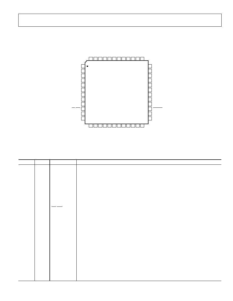
PIN CONFIGURATION AND FUNCTION DESCRIPTIONS
AV
DD
48
LF
47
ADC2RN
46
ADC2RP
45
ADC2L
N
44
ADC2L
P
43
ADC1RN
42
ADC1RP
41
ADC1L
N
40
ADC1L
P
39
CM
38
AV
DD
37
DV
DD
13
DS
DAT
A3
14
DS
DAT
A2
15
DS
DAT
A1
16
DBC
L
K
17
D
L
RCL
K
18
AS
DAT
A2
19
AS
DAT
A1
20
ABC
L
K
21
A
L
RCL
K
22
CI
N/
ADR0
23
CO
UT
/
S
D
A
24
AGND
1
MCLKI/XI
2
MCLKO/XO
3
AGND
4
AVDD
5
OL3
6
OR3
7
OL4
8
OR4
9
PD/RST
10
DSDATA4
11
DGND
12
AGND
36
FILTR
35
AGND
34
AVDD
33
AGND
32
OR2
31
OL2
30
OR1
29
OL1
28
CLATCH/ADR1
27
CCLK/SCL
26
DGND
25
ADAU1328
TOP VIEW
(Not to Scale)
SINGLE-ENDED
OUTPUT
06
10
2-
0
20
Figure 2. Pin Configuration
Table 9. Pin Function Description
Pin No.
In/Out
Mnemonic
Description
1 I AGND
Analog
Ground.
2
I
MCLKI/XI
Master Clock Input/Crystal Oscillator Input.
3
O
MCLKO/XO
Master Clock Output/Crystal Oscillator Output.
4 I AGND
Analog
Ground.
5
I
AVDD
Analog Power Supply. Connect to analog 3.3 V supply.
6
O
OL3
DAC 3 Left Output.
7
O
OR3
DAC 3 Right Output.
8
O
OL4
DAC 4 Left Output.
9
O
OR4
DAC 4 Right Output.
10 I PD/RST
Power-Down Reset (Active Low).
11
I/O
DSDATA4
DAC Input 4 (Input to DAC 4 L and R)/DAC TDM Data Out 2/AUX ADC 1 Data In.
12 I DGND
Digital
Ground.
13
I
DVDD
Digital Power Supply. Connect to digital 3.3 V supply.
14
I/O
DSDATA3
DAC Input 3 (Input to DAC 3 L and R)/DAC TDM Data In 2/AUX DAC 2 Data Output.
15
I/O
DSDATA2
DAC Input 2 (Input to DAC 2 L and R)/DAC TDM Data Out 1/AUX ADC 1 Data In.
16
I
DSDATA1
DAC Input 1 (Input to DAC 1 L and R)/DAC TDM Data In 1/AUX ADC 2 Data In.
17
I/O
DBCLK
Bit Clock for DACs.
18
I/O
DLRCLK
LR Clock for DACs.
19
I/O
ASDATA2
ADC Serial Data Output 2 (ADC 2 L and R)/ADC TDM Data Input/AUX DAC 1 Data Output.
20
O
ASDATA1
ADC Serial Data Output 1 (ADC 1 L and R)/ADC TDM Data Output.
21
I/O
ABCLK
Bit Clock for ADCs.
22
I/O
ALRCLK
LR Clock for ADCs.
23
I
CIN/ADR0
Control Data Input (SPI).
24
I/O
COUT/SDA
Control Data Output (SPI).
25 I DGND
Digital
Ground.
ADAU1328
Rev. 0 | Page 10 of 32
Pin No.
In/Out
Mnemonic
Description
26
I
CCLK/SCL
Control Clock Input (SPI).
27 I CLATCH/ADR1
Latch Input for Control Data (SPI).
28
O
OL1
DAC 1 Left Output.
29
O
OR1
DAC 1 Right Output.
30
O
OL2
DAC 2 Left Output.
31
O
OR2
DAC 2 Right Output.
32 I AGND
Analog
Ground.
33
I
AVDD
Analog Power Supply. Connect to analog 3.3 V supply.
34 I AGND
Analog
Ground.
35
O
FILTR
Voltage Reference Filter Capacitor Connection. Bypass with 10 F||100 nF to AGND.
36 I AGND
Analog
Ground.
37
I
AVDD
Analog Power Supply. Connect to analog 3.3 V supply.
38
O
CM
Common-Mode Reference Filter Capacitor Connection. Bypass with 47 F||100 nF to AGND.
39
I
ADC1LP
ADC1 Left Positive Input.
40
I
ADC1LN
ADC1 Left Negative Input.
41
I
ADC1RP
ADC1 Right Positive Input.
42
I
ADC1RN
ADC1 Right Negative Input.
43
I
ADC2LP
ADC2 Left Positive Input.
44
I
ADC2LN
ADC2 Left Negative Input.
45
I
ADC2RP
ADC2 Right Positive Input.
46
I
ADC2RN
ADC2 Right Negative Input.
47
O
LF
PLL Loop Filter. Return to AVDD.
48
I
AVDD
Analog Power Supply. Connect to analog 3.3 V supply.
ADAU1328
Rev. 0 | Page 11 of 32
TYPICAL PERFORMANCE CHARACTERISTICS
0.10
0.08
0.06
0.04
0.02
0
≠0.10
≠0.08
≠0.06
≠0.04
≠0.02
0
18000
16000
14000
12000
10000
8000
6000
4000
2000
M
AG
NI
T
UDE
(
d
B)
FREQUENCY (Hz)
0
610
2-
00
2
Figure 3. ADC Pass-Band Filter Response, 48 kHz
0
≠10
≠20
≠30
≠40
≠50
≠60
≠70
≠80
≠90
≠100
0
40000
5000 10000 15000 20000 25000 30000 35000
M
AG
NI
T
UD
E
(
d
B)
FREQUENCY (Hz)
06
10
2-
0
03
Figure 4. ADC Stop-Band Filter Response, 48 kHz
0.06
0.04
0.02
≠0.06
≠0.04
≠0.02
0
0
24
0
610
2-
00
4
8
16
8
M
AG
NI
T
UDE
(
d
B)
FREQUENCY (kHz)
Figure 5. DAC Pass-Band Filter Response, 48 kHz
0
≠150
≠100
≠50
0
4
12
24
36
MA
G
N
I
T
U
D
E
(d
B
)
FREQUENCY (kHz)
06
10
2-
0
05
Figure 6. DAC Stop-Band Filter Response, 48 kHz
0.10
≠0.10
≠0.05
0
0.05
0
9
72
48
24
M
AG
NI
T
UDE
(
d
B)
FREQUENCY (kHz)
6
0
610
2-
00
6
Figure 7. DAC Pass-Band Filter Response, 96 kHz
0
≠150
≠100
≠50
0
96
24
48
72
MA
G
N
I
T
U
D
E
(d
B
)
FREQUENCY (kHz)
06
10
2-
0
07
Figure 8. DAC Stop-Band Filter Response, 96 kHz
ADAU1328
Rev. 0 | Page 12 of 32
4
0.5
≠0.5
≠0.4
≠0.3
≠0.2
≠0.1
0
0.1
0.2
0.3
0.4
0
6
8
16
32
MA
G
N
I
T
U
D
E
(d
B
)
FREQUENCY (kHz)
06
10
2-
0
08
≠10
≠8
≠6
≠4
≠2
0
48
96
64
80
MA
G
N
I
T
U
D
E
(d
B
)
FREQUENCY (kHz)
06
10
2-
0
09
Figure 10. DAC Stop-Band Filter Response, 192 kHz
Figure 9. DAC Pass-Band Filter Response, 192 kHz

ADAU1328
Rev. 0 | Page 13 of 32
THEORY OF OPERATION
ANALOG-TO-DIGITAL CONVERTERS (ADCs)
There are two ADC channels in the ADAU1328 configured as
two stereo pairs with differential inputs. The ADCs can operate
at a nominal sample rate of 48 kHz, 96 kHz, or 192 kHz. The
ADCs include on-board digital antialiasing filters with 79 dB
stop-band attenuation and linear phase response, operating at
an oversampling ratio of 128 (48 kHz, 96 kHz, and 192 kHz
modes). Digital outputs are supplied through two serial data
output pins (one for each stereo pair) and a common frame
(ALRCLK) and bit (ABCLK) clock. Alternatively, one of the
TDM modes can be used to access up to 16 channels on a single
TDM data line.
The ADCs must be driven from a differential signal source for
best performance. The input pins of the ADCs connect to
internal switched capacitors. To isolate the external driving op
amp from the glitches caused by the internal switched capacitors,
each input pin should be isolated by using a series connected,
external, 100 resistor together with a 1 nF capacitor connected
from each input to ground. This capacitor must be of high quality,
for example, ceramic NPO or polypropylene film.
The differential inputs have a nominal common-mode voltage
of 1.5 V. The voltage at the common-mode reference pin (CM)
can be used to bias external op amps to buffer the input signals
(see the Power Supply and Voltage Reference section). The
inputs can also be ac-coupled and do not need an external dc
bias to CM.
A digital high-pass filter can be switched in line with the ADCs
under serial control to remove residual dc offsets. It has a
1.4 Hz, 6 dB per octave cutoff at a 48 kHz sample rate. The
cutoff frequency scales directly with sample frequency.
DIGITAL-TO-ANALOG CONVERTERS (DACs)
The ADAU1328 DAC channels are arranged as single-ended,
four stereo pairs giving eight analog outputs for minimum
external components. The DACs include on-board digital
reconstruction filters with 70 dB stop-band attenuation and linear
phase response, operating at an oversampling ratio of 4 (48 kHz or
96 kHz modes) or 2 (192 kHz mode). Each channel has its own
independently programmable attenuator, adjustable in 255 steps
in increments of 0.375 dB. Digital inputs are supplied through
four serial data input pins (one for each stereo pair) and a
common frame (DLRCLK) and bit (DBCLK) clock. Alternatively,
one of the TDM modes can be used to access up to 16 channels
on a single TDM data line.
Each output pin has a nominal common-mode dc level of 1.5 V
and swings ±1.27 V for a 0 dBFS digital input signal. A single op
amp, third-order, external, low-pass filter is recommended to
remove high frequency noise present on the output pins. The
use of op amps with low slew rate or low bandwidth can cause
high frequency noise and tones to fold down into the audio
band; therefore, exercise care in selecting these components.
The voltage at CM, the common-mode reference pin, can be
used to bias the external op amps that buffer the output signals
(see the Power Supply and Voltage Reference section).
CLOCK SIGNALS
The on-chip phase locked loop (PLL) can be selected to
reference the input sample rate from either of the LRCLK pins
or 256, 384, 512, or 768 times the sample rate, referenced to the
48 kHz mode from the MCLKI pin. The default at power-up is
256 ◊ f
S
from MCLKI. In 96 kHz mode, the master clock fre-
quency stays at the same absolute frequency; therefore, the
actual multiplication rate is divided by 2. In 192 kHz mode,
the actual multiplication rate is divided by 4. For example, if a
device in the ADAU1328 family is programmed in 256 ◊ f
S
mode,
the frequency of the master clock input is 256 ◊ 48 kHz =
12.288 MHz. If the ADAU1328 is then switched to 96 kHz
operation (by writing to the SPI or I
2
C port), the frequency of
the master clock should remain at 12.288 MHz, which is now
128 ◊ f
S
. In 192 kHz mode, this becomes 64 ◊ f
S
.
The internal clock for the ADCs is 256 ◊ f
S
for all clock modes.
The internal clock for the DACs varies by mode: 512 ◊ f
S
(48 kHz
mode), 256 ◊ f
S
(96 kHz mode), or 128 ◊ f
S
(192 kHz mode). By
default, the on-board PLL generates this internal master clock
from an external clock. A direct 512 ◊ f
S
(referenced to 48 kHz
mode) master clock can be used for either the ADCs or DACs if
selected in PLL and Clock Control 1 Register.
Note that it is not possible to use a direct clock for the ADCs set
to the 192 kHz mode. It is required that the on-chip PLL be
used in this mode.
The PLL can be powered down in PLL and Clock Control 0
Register. To ensure reliable locking when changing PLL modes,
or if the reference clock is unstable at power-on, power down
the PLL and then power it back up when the reference clock has
stabilized.
The internal MCLK can be disabled in PLL and Clock Control 0
Register to reduce power dissipation when the ADAU1328 is
idle. The clock should be stable before it is enabled. Unless a
standalone mode is selected (see the Serial Control Port
section), the clock is disabled by reset and must be enabled by
writing to the SPI or I
2
C port for normal operation.

ADAU1328
Rev. 0 | Page 14 of 32
To maintain the highest performance possible, it is recommended
that the clock jitter of the internal master clock signal be limited
to less than 300 ps rms time interval error (TIE). Even at these
levels, extra noise or tones can appear in the DAC outputs if the
jitter spectrum contains large spectral peaks. If the internal PLL
is not being used, it is highly recommended that an independent
crystal oscillator generate the master clock. In addition, it is
especially important that the clock signal not be passed through
an FPGA, CPLD, or other large digital chip (such as a DSP)
before being applied to the ADAU1328. In most cases, this
induces clock jitter due to the sharing of common power and
ground connections with other unrelated digital output signals.
When the PLL is used, jitter in the reference clock is attenuated
above a certain frequency depending on the loop filter.
RESET AND POWER-DOWN
Reset sets all the control registers to their default settings. To
avoid pops, reset does not power down the analog outputs.
After reset is deasserted, and the PLL acquires lock condition,
an initialization routine runs inside the ADAU1328. This
initialization lasts for approximately 256 MCLKs.
The power-down bits in the PLL and Clock Control 0, DAC
Control 1, and ADC Control 1 registers power down the
respective sections. All other register settings are retained.
The reset pin should be pulled low by an external resistor to
guarantee proper startup.
SERIAL CONTROL PORT
The ADAU1328 has an SPI control port that permits
programming and reading back of the internal control registers
for the ADCs, DACs, and clock system. There is also a stand-
alone mode available for operation without serial control that is
configured at reset using the serial control pins. All registers are
set to default, except the internal MCLK enable is set to 1 and
ADC BCLK and LRCLK master/slave is set by COUT/SDA.
Refer to Table 10 for details. It is recommended to use a weak
pull-up resistor on CLATCH in applications that have a
microcontroller. This pull-up resistor ensures that the
ADAU1328 recognizes the presence of a microcontroller.
The SPI control port of the ADAU1328 is a 4-wire serial control
port. The format is similar to the Motorola SPI format except
the input data-word is 24 bits wide. The serial bit clock and
latch can be completely asynchronous to the sample rate of the
ADCs and DACs. Figure 11 shows the format of the SPI signal.
The first byte is a global address with a read/write bit. For the
ADAU1328, the address is 0x04, shifted left 1 bit due to the
R/W bit. The second byte is the ADAU1328 register address
and the third byte is the data.
Table 10. Standalone Mode Selection
ADC Clocks
CIN/ADR0
COUT/SDA
CCLK/SCL
CLATCH/ADR1
Slave 0 0
0 0
Master 0
1
0 0
D0
D0
D8
D8
D22
D23
D9
D9
CLATCH
CCLK
CIN
COUT
t
CCH
t
CCL
t
CDS
t
CDH
t
CLS
t
CCP
t
CLH
t
COTS
t
COD
t
COE
06
10
2-
0
10
Figure 11. Format of SPI Signal
ADAU1328
Rev. 0 | Page 15 of 32
POWER SUPPLY AND VOLTAGE REFERENCE
The ADAU1328 is designed for 3.3 V supplies. Separate power
supply pins are provided for the analog and digital sections.
These pins should be bypassed with 100 nF ceramic chip
capacitors, as close to the pins as possible, to minimize noise
pickup. A bulk aluminum electrolytic capacitor of at least 22 F
should also be provided on the same PC board as the codec. For
critical applications, improved performance is obtained with
separate supplies for the analog and digital sections. If this is
not possible, it is recommended that the analog and digital
supplies be isolated by means of a ferrite bead in series with each
supply. It is important that the analog supply be as clean as possible.
All digital inputs are compatible with TTL and CMOS levels.
All outputs are driven from the 3.3 V DVDD supply and are
compatible with TTL and 3.3 V CMOS levels.
The ADC and DAC internal voltage reference (VREF) is brought
out on FILTR and should be bypassed as close as possible to the
chip, with a parallel combination of 10 F and 100 nF. Any
external current drawn should be limited to less than 50 A.
The internal reference can be disabled in PLL and Clock
Control 1 Register, and FILTR can be driven from an external
source. This can be used to scale the DAC output to the clipping
level of a power amplifier based on its power supply voltage.
The ADC input gain varies by the inverse ratio. The total gain
from ADC input to DAC output remains constant.
The CM pin is the internal common-mode reference. It should
be bypassed as close as possible to the chip, with a parallel
combination of 47 F and 100 nF. This voltage can be used to
bias external op amps to the common-mode voltage of the input
and output signal pins. The output current should be limited to
less than 0.5 mA source and 2 mA sink.
SERIAL DATA PORTS--DATA FORMAT
The eight DAC channels use a common serial bit clock (DBCLK)
and a common left-right framing clock (DLRCLK) in the serial
data port. The four ADC channels use a common serial bit clock
(ABCLK) and left-right framing clock (ALRCLK) in the serial
data port. The clock signals are all synchronous with the sample
rate. The normal stereo serial modes are shown in Figure 23.
The ADC and DAC serial data modes default to I
2
S. The ports
can also be programmed for left justified, right justified, and
TDM modes. The word width is 24 bits by default and can be
programmed for 16 or 20 bits. The DAC serial formats are
programmable according to DAC Control 0 Register. The
polarity of the DBCLK and DLRCLK is programmable according
to DAC Control 1 Register. The ADC serial formats and serial
clock polarity are programmable according to ADC Control 1
Register. Both DAC and ADC serial ports are programmable to
become the bus masters according to DAC Control 1 Register
and Control 2 Register. By default, both ADC and DAC serial
ports are in the slave mode.
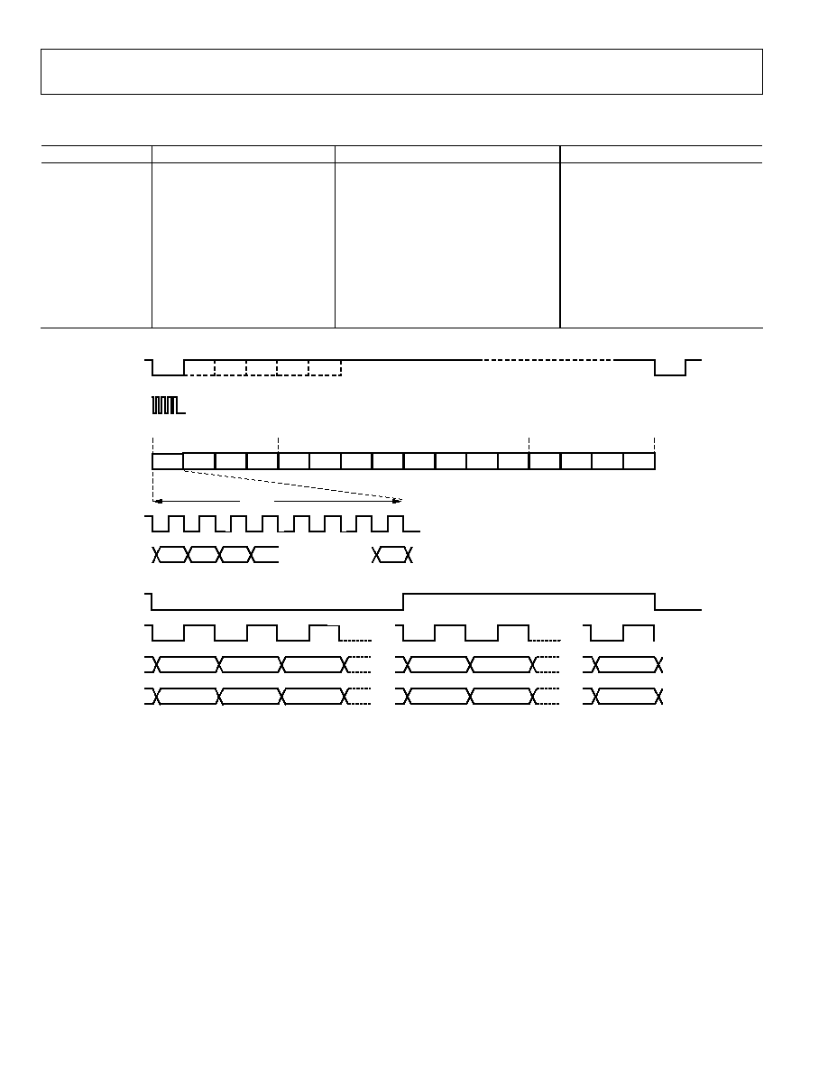
TIME-DIVISION MULTIPLEXED (TDM) MODES
The ADAU1328 serial ports also have several different TDM
serial data modes. The first and most commonly used
configurations are shown in Figure 12 and Figure 13. In Figure 12,
the ADC serial port outputs one data stream consisting of four
on-chip ADCs followed by four unused slots. In Figure 13, the
eight on-chip DAC data slots are packed into one TDM stream.
In this mode, both DBCLK and ABCLK are 256 f
S
.
The I/O pins of the serial ports are defined according to the
serial mode selected. For a detailed description of the function
of each pin in TDM and AUX modes, see Table 11.
The ADAU1328 allows systems with more than eight DAC
channels to be easily configured by the use of an auxiliary serial
data port. The DAC TDM-AUX mode is shown in Figure 14. In
this mode, the AUX channels are the last four slots of the TDM
data stream. These slots are extracted and output to the AUX serial
port. It should be noted that due to the high DBCLK frequency, this
mode is available only in the 48 kHz/44.1 kHz/32 kHz sample rate.
The ADAU1328 also allows system configurations with more
than four ADC channels, as shown in Figure 15 and Figure 16,
which show using 8 ADCs and 16 ADCs, respectively. Again,
due to the high ABCLK frequency, this mode is available only
in the 48 kHz/44.1 kHz/32 kHz sample rate.
Combining the AUX DAC and ADC modes results in a system
configuration of 8 ADCs and 12 DACs. The system, then, con-
sists of two external stereo ADCs, two external stereo DACs,
and one ADAU1328. This mode is shown in Figure 17
(combined AUX DAC and ADC modes).
SLOT 1
LEFT 1
SLOT 2
RIGHT 1
SLOT 3
LEFT 2
SLOT 4
RIGHT 2
MSB
MSB≠1
MSB≠2
DATA
BCLK
LRCLK
SLOT 5
SLOT 6
SLOT 7
SLOT 8
LRCLK
BCLK
DATA
256 BCLKs
32 BCLKs
06102-
016
Figure 12. ADC TDM (8-Channel I
2
S Mode)
SLOT 1
LEFT 1
SLOT 2
RIGHT 1
SLOT 3
LEFT 2
SLOT 4
RIGHT 2
MSB
MSB≠1
MSB≠2
DATA
BCLK
LRCLK
SLOT 5
LEFT 3
SLOT 6
RIGHT 3
SLOT 7
LEFT 4
SLOT 8
RIGHT 4
LRCLK
BCLK
DATA
256 BCLKs
32 BCLK
06
102-
017
Figure 13. DAC TDM (8-Channel I
2
S Mode)
ADAU1328
Rev. 0 | Page 16 of 32
Table 11. Pin Function Changes in TDM and AUX Modes
Mnemonic
Stereo Modes
TDM Modes
AUX Modes
ASDATA1
ADC1 Data Out
ADC TDM Data Out
TDM Data Out
ASDATA2
ADC2 Data Out
ADC TDM Data In
AUX Data Out 1 (to External DAC 1)
DSDATA1
DAC1 Data In
DAC TDM Data In
TDM Data In
DSDATA2
DAC2 Data In
DAC TDM Data Out
AUX Data In 1 (from External ADC 1)
DSDATA3
DAC3 Data In
DAC TDM Data In 2 (Dual-Line Mode)
AUX Data In 2 (from External ADC 2)
DSDATA4
DAC4 Data In
DAC TDM Data Out 2 (Dual-Line Mode)
AUX Data Out 2 (to External DAC 2)
ALRCLK
ADC LRCLK In/Out
ADC TDM Frame Sync In/Out
TDM Frame Sync In/Out
ABCLK
ADC BCLK In/Out
ADC TDM BCLK In/Out
TDM BCLK In/Out
DLRCLK
DAC LRCLK In/Out
DAC TDM Frame Sync In/Out
AUX LRCLK In/Out
DBCLK
DAC BCLK In/Out
DAC TDM BCLK In/Out
AUX BCLK In/Out
LEFT
RIGHT
MSB
MSB
MSB
MSB
ALRCLK
ABCLK
DSDATA1
(TDM_IN)
DLRCLK
(AUX PORT)
DBCLK
(AUX PORT)
ASDATA2
(AUX1_OUT)
DSDATA4
(AUX2_OUT)
MSB
EMPTY
EMPTY
EMPTY
EMPTY
DAC L1 DAC R1 DAC L2 DAC R2 DAC L3 DAC R3 DAC L4 DAC R4 AUX L1 AUX R1 AUX L2 AUX R2
8-ON-CHIP DAC CHANNELS
AUXILIARY DAC CHANNELS
WILL APPEAR AT
AUX DAC PORTS
UNUSED SLOTS
32 BITS
0
61
02
-
051
Figure 14. 16-Channel DAC TDM-AUX Mode

ADAU1328
Rev. 0 | Page 17 of 32
ALRCLK
ABCLK
DSDATA1
(TDM_IN)
ASDATA1
(TDM_OUT)
DLRCLK
(AUX PORT)
DBCLK
(AUX PORT)
DSDATA2
(AUX1_IN)
DSDATA3
(AUX2_IN)
DAC L1
DAC R1
DAC L2
DAC R2
DAC L3
DAC R3
DAC L4
DAC R4
ADC L1
ADC R1
ADC L2
ADC R2
AUX L1
AUX R1
AUX L2
AUX R2
8-ON-CHIP DAC CHANNELS
4-ON-CHIP ADC CHANNELS
4-AUX ADC CHANNELS
32 BITS
LEFT
RIGHT
MSB
MSB
MSB
MSB
MSB
0
61
02
-
05
0
Figure 15. 8-Channel AUX ADC Mode
LEFT
RIGHT
MSB
MSB
MSB
MSB
DLRCLK
(AUX PORT)
DBCLK
(AUX PORT)
DSDATA2
(AUX1_IN)
DSDATA3
(AUX2_IN)
ALRCLK
ABCLK
ASDATA1
(TDM_OUT)
MSB
ADC L1 ADC R1 ADC L2 ADC R2 AUX L1 AUX R1 AUX L2 AUX R2
UNUSED UNUSED UNUSED UNUSED
UNUSED UNUSED UNUSED UNUSED
4 ON-CHIP ADC CHANNELS
AUXILIARY ADC CHANNELS
UNUSED SLOTS
32 BITS
06
10
2-
0
52
Figure 16. 16-Channel AUX ADC Mode
ADAU1328
Rev. 0 | Page 18 of 32
LEFT
RIGHT
DLRCLK
(AUX PORT)
DBCLK
(AUX PORT)
MSB
MSB
DSDATA2
(AUX1_IN)
MSB
MSB
DSDATA3
(AUX2_IN)
MSB
MSB
ASDATA2
(AUX1_OUT)
MSB
MSB
DSDATA4
(AUX2_OUT)
ALRCLK
ABCLK
DSDATA1
(TDM_IN)
EMPTY
EMPTY
EMPTY
EMPTY
DAC L1 DAC R1 DAC L2 DAC R2 DAC L3 DAC R3 DAC L4 DAC R4 AUX L1 AUX R1 AUX L2 AUX R2
8 ON-CHIP DAC CHANNELS
AUXILIARY DAC CHANNELS
APPEAR AT
AUX DAC PORTS
UNUSED SLOTS
ASDATA1
(TDM_OUT)
ADC L1 ADC R1 ADC L2 ADC R2
AUX L1 AUX R1 AUX L2 AUX R2
UNUSED UNUSED UNUSED UNUSED
UNUSED UNUSED UNUSED UNUSED
4 ON-CHIP ADC CHANNELS
AUXILIARY ADC CHANNELS
UNUSED SLOTS
0
61
02
-
05
3
Figure 17. Combined AUX DAC and ADC Mode

ADAU1328
Rev. 0 | Page 19 of 32
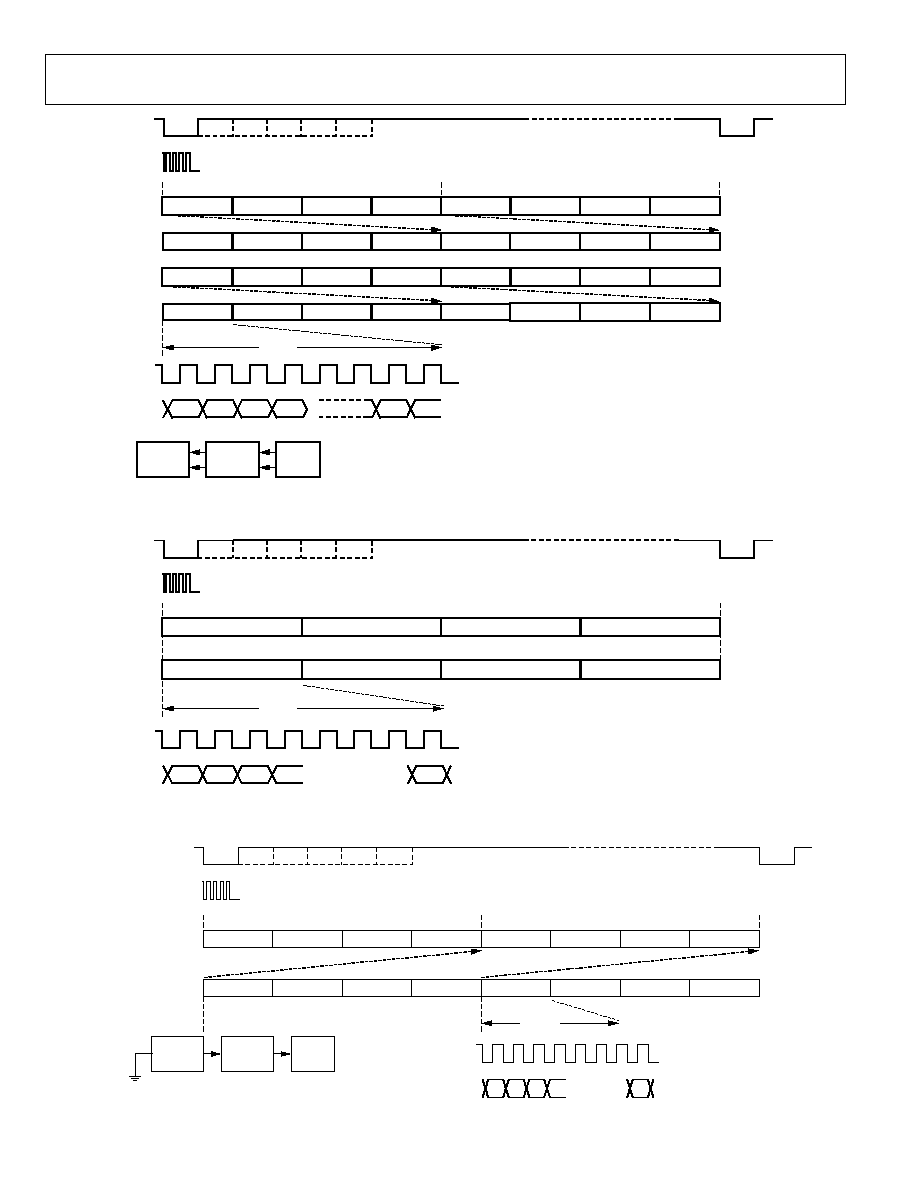
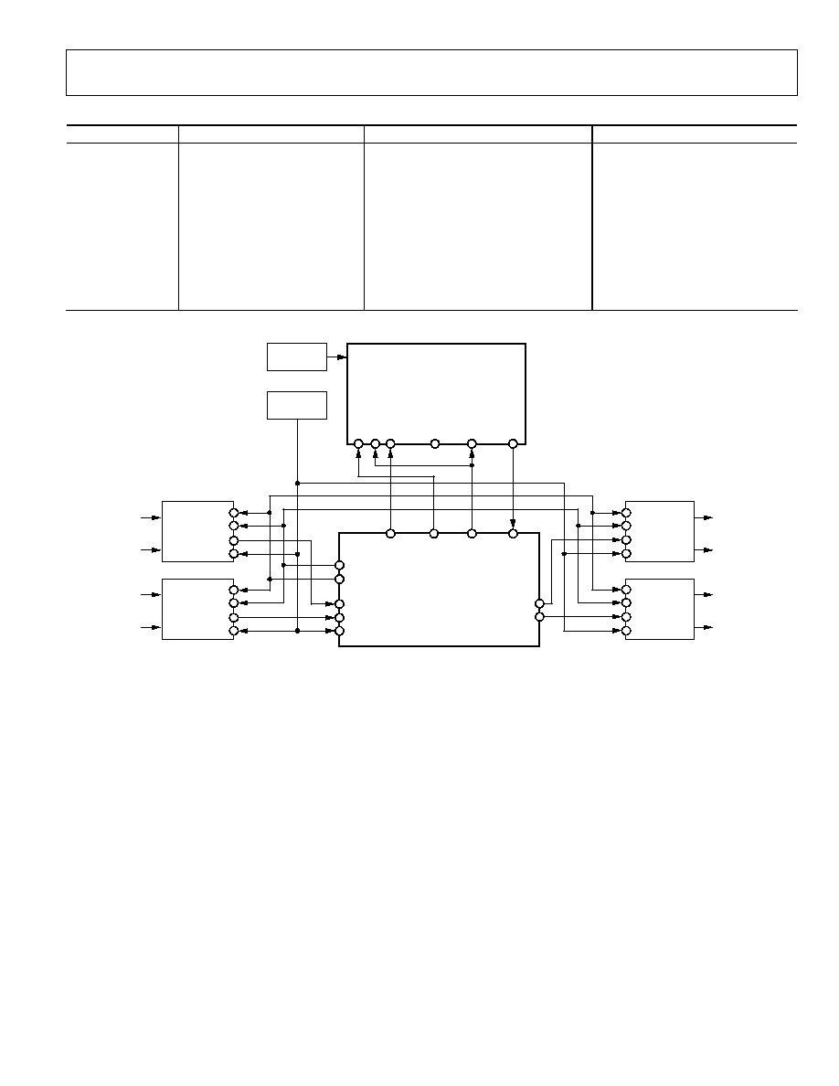
DAISY-CHAIN MODE
The ADAU1328 also allows a daisy-chain configuration to
expand the system to 8 ADCs and 16 DACs (see Figure 18). In
this mode, the DBCLK frequency is 512 f
S
. The first eight slots
of the DAC TDM data stream belong to the first ADAU1328 in
the chain and the last eight slots belong to the second ADAU1328.
The second ADAU1328 is the device attached to the DSP
TDM port.
To accommodate 16 channels at a 96 kHz sample rate, the
ADAU1328 can be configured into a dual-line, DAC TDM
mode, as shown in Figure 19. This mode allows a slower
DBCLK than normally required by the one-line TDM mode.
Again, the first four channels of each TDM input belong to the
first ADAU1328 in the chain and the last four channels belong
to the second ADAU1328.
The dual-line TDM mode can also be used to send data at a
192 kHz sample rate into the ADAU1328, as shown in Figure 20.
There are two configurations for the ADC port to work in
daisy-chain mode. The first one is with an ABCLK at 256 f
S
shown in Figure 21. The second configuration is shown in
Figure 22. Note that in the 512 f
S
ABCLK mode, the ADC
channels occupy the first eight slots; the second eight slots are
empty. The TDM_IN of the first ADAU1328 must be grounded
in all modes of operation.
The I/O pins of the serial ports are defined according to the
serial mode selected. See Table 12 for a detailed description of
the function of each pin. See Figure 26 for a typical ADAU1328
configuration with two external stereo DACs and two external
stereo ADCs.
Figure 23 through Figure 25 show the serial mode formats. For
maximum flexibility, the polarity of LRCLK and BCLK are
programmable. In these figures, all of the clocks are shown with
their normal polarity. The default mode is I
2
S.
DLRCLK
DBCLK
8 DAC CHANNELS OF THE FIRST IC IN THE CHAIN
8 UNUSED SLOTS
8 DAC CHANNELS OF THE SECOND IC IN THE CHAIN
MSB
DSDATA1 (TDM_IN)
OF THE SECOND ADAU1328
DSDATA2 (TDM_OUT)
OF THE SECOND ADAU1328
THIS IS THE TDM
TO THE FIRST ADAU1328
DAC L1 DAC R1 DAC L2 DAC R2 DAC L3 DAC R3 DAC L4 DAC R4 DAC L1 DAC R1 DAC L2 DAC R2 DAC L3 DAC R3 DAC L4 DAC R4
DAC L1 DAC R1 DAC L2 DAC R2 DAC L3 DAC R3 DAC L4 DAC R4
32 BITS
DSP
SECOND
ADAU1328
FIRST
ADAU1328
06
10
2-
0
54
Figure 18. Single-Line DAC TDM Daisy-Chain Mode (Applicable to 48 kHz Sample Rate, 16-Channel, Two ADAU1328 Daisy Chain)
ADAU1328
Rev. 0 | Page 20 of 32
DLRCLK
DBCLK
8 DAC CHANNELS OF THE SECOND IC IN THE CHAIN
8 DAC CHANNELS OF THE FIRST IC IN THE CHAIN
DSDATA1
(IN)
DAC L1
DAC R1
DAC L2
DAC R2
DAC L1
DAC R1
DAC L2
DAC R2
DSDATA3
(IN)
DAC L3
DAC R3
DAC L4
DAC R4
DAC L3
DAC R3
DAC L4
DAC R4
DSDATA2
(OUT)
DAC L1
DAC R1
DAC L2
DAC R2
DSDATA4
(OUT)
DAC L3
DAC R3
DAC L4
DAC R4
32 BITS
DSP
SECOND
ADAU1328
FIRST
ADAU1328
MSB
06
10
2-
05
5
Figure 19. Dual-Line DAC TDM Mode (Applicable to 96 kHz Sample Rate, 16-Channel, Two ADAU1328 Daisy Chain); DSDATA3 and DSDATA4 Are the Daisy Chain
DLRCLK
DBCLK
DSDATA1
DAC L1
DAC R1
DAC L2
DAC R2
DSDATA2
DAC L3
DAC R3
DAC L4
DAC R4
32 BITS
MSB
06
10
2-
0
58
Figure 20. Dual-Line DAC TDM Mode (Applicable to 192 kHz Sample Rate, 8-Channel Mode)
ALRCLK
ABCLK
ASDATA2 (TDM_IN
OF THE SECOND ADAU1328
IN THE CHAIN)
ADC L1
ADC R1
ADC L2
ADC R2
4 ADC CHANNELS OF FIRST IC IN THE CHAIN
4 ADC CHANNELS OF SECOND IC IN THE CHAIN
ASDATA1 (TDM_OUT
OF THE SECOND ADAU1328
IN THE CHAIN)
ADC L1
ADC R1
ADC L2
ADC R2
ADC L1
ADC R1
ADC L2
ADC R2
32 BITS
MSB
DSP
SECOND
ADAU1328
FIRST
ADAU1328
0
610
2-
0
56
Figure 21. Dual-Line ADC TDM Daisy-Chain Mode (256 f
S
ABCLK, Two ADAU1328 Daisy Chain)

ADAU1328
Rev. 0 | Page 21 of 32
ALRCLK
ABCLK
4 ADC CHANNELS OF
SECOND IC IN THE CHAIN
4 ADC CHANNELS OF
FIRST IC IN THE CHAIN
ADC L1 ADC R1 ADC L2 ADC R2 ADC L1 ADC R1 ADC L2 ADC R2
ASDATA1 (TDM_OUT
OF THE SECOND ADAU1328
IN THE CHAIN)
ADC L1 ADC R1 ADC L2 ADC R2
ASDATA2 (TDM_IN
OF THE SECOND ADAU1328
IN THE CHAIN)
32 BITS
MSB
DSP
SECOND
ADAU1328
FIRST
ADAU1328
06
10
2-
0
57
Figure 22. Dual-Line ADC TDM Daisy-Chain Mode (512 f
S
ABCLK, Two ADAU1328 Daisy Chain)
LRCLK
BCLK
SDATA
LRCLK
BCLK
SDATA
LRCLK
BCLK
SDATA
LSB
LSB
LSB
LSB
LSB
LSB
LEFT CHANNEL
RIGHT CHANNEL
RIGHT CHANNEL
LEFT CHANNEL
LEFT CHANNEL
RIGHT CHANNEL
MSB
MSB
MSB
MSB
MSB
MSB
RIGHT-JUSTIFIED MODE--SELECT NUMBER OF BITS PER CHANNEL
DSP MODE--16 BITS TO 24 BITS PER CHANNEL
I
2
S MODE--16 BITS TO 24 BITS PER CHANNEL
LEFT-JUSTIFIED MODE--16 BITS TO 24 BITS PER CHANNEL
LRCLK
BCLK
SDATA
LSB
LSB
NOTES
1. DSP MODE DOES NOT IDENTIFY CHANNEL.
2. LRCLK NORMALLY OPERATES AT
f
S
EXCEPT FOR DSP MODE, WHICH IS 2 ◊
f
S
.
3. BCLK FREQUENCY IS NORMALLY 64 ◊ LRCLK BUT MAY BE OPERATED IN BURST MODE.
MSB
MSB
1/
f
S
06
102
-
0
13
Figure 23. Stereo Serial Modes

ADAU1328
Rev. 0 | Page 22 of 32
DBCLK
DLRCLK
DSDATA
LEFT-JUSTIFIED
MODE
DSDATA
RIGHT-JUSTIFIED
MODE
DSDATA
I
2
S-JUSTIFIED
MODE
t
DLH
t
DBH
t
DBL
t
DLS
t
DDS
MSB
MSB
MSB
LSB
MSB≠1
t
DDH
t
DDS
t
DDH
t
DDS
t
DDH
t
DDH
t
DDS
0
610
2-
014
Figure 24. DAC Serial Timing
ABCLK
ALRCLK
ASDATA
LEFT-JUSTIFIED
MODE
ASDATA
RIGHT-JUSTIFIED
MODE
ASDATA
I
2
S-JUSTIFIED
MODE
t
ABH
LSB
MSB
MSB
MSB
MSB≠1
t
ABL
t
ALS
t
ABDD
t
ABDD
t
ABDD
t
ALH
06
10
2-
0
15
Figure 25. ADC Serial Timing
ADAU1328
Rev. 0 | Page 23 of 32
Table 12. Pin Function Changes in TDM and AUX Modes (Replication of Table 11)
Mnemonic
Stereo Modes
TDM Modes
AUX Modes
ASDATA1
ADC1 Data Out
ADC TDM Data Out
TDM Data Out
ASDATA2
ADC2 Data Out
ADC TDM Data In
AUX Data Out 1 (to External DAC 1)
DSDATA1
DAC1 Data In
DAC TDM Data In
TDM Data In
DSDATA2
DAC2 Data In
DAC TDM Data Out
AUX Data In 1 (from External ADC 1)
DSDATA3
DAC3 Data In
DAC TDM Data In 2 (Dual-Line Mode)
AUX Data In 2 (from External ADC 2)
DSDATA4
DAC4 Data In
DAC TDM Data Out 2 (Dual-Line Mode)
AUX Data Out 2 (to External DAC 2)
ALRCLK
ADC LRCLK In/Out
ADC TDM Frame Sync In/Out
TDM Frame Sync In/Out
ABCLK
ADC BCLK In/Out
ADC TDM BCLK In/Out
TDM BCLK In/Out
DLRCLK
DAC LRCLK In/Out
DAC TDM Frame Sync In/Out
AUX LRCLK In/Out
DBCLK
DAC BCLK In/Out
DAC TDM BCLK In/Out
AUX BCLK In/Out
AUX
ADC 1
LRCLK
BCLK
DATA
MCLK
AUX
ADC 2
LRCLK
BCLK
DATA
MCLK
AUX
DAC 1
AUX
DAC 2
LRCLK
BCLK
DATA
MCLK
LRCLK
BCLK
DATA
MCLK
30MHz
12.288MHz
SHARC IS RUNNING IN SLAVE MODE
(INTERRUPT-DRIVEN)
SHARC
ADAU1328
TDM MASTER
AUX MASTER
F
S
Y
N
C
-
TD
M (
R
FS
)
RxCL
K
RxDAT
A
Tx
C
L
K
Tx
D
A
TA
T
F
S
(
NC)
ASDATA2
DSDATA4
DBCLK
DLRCLK
DSDATA2
DSDATA3
MCLK
ASDATA1 ALRCLK ABCLK DSDATA1
06
10
2-
0
19
Figure 26. Example of AUX Mode Connection to SHARCÆ (ADAU1328 as TDM Master/AUX Master Shown)

ADAU1328
Rev. 0 | Page 24 of 32
CONTROL REGISTERS
DEFINITIONS
The format is the same for I
2
C and SPI ports. The global address for the ADAU1328 is 0x04, shifted left 1 bit due to the R/W bit. However,
in I
2
C, ADR0 and ADR1 are OR'ed into Bit 17 and Bit 8 to provide multiple chip addressing. All registers are reset to 0, except for the
DAC volume registers that are set to full volume.
Note that the first setting in each control register parameter is the default setting.
Table 13. Register Format
Global
Address
R/W
Register Address
Data
Bit
23:17 16
15:8
7:0
Table 14. Register Addresses and Functions
Address Function
0
PLL and Clock Control 0
1
PLL and Clock Control 1
2
DAC Control 0
3
DAC Control 1
4
DAC Control 2
5
DAC individual channel mutes
6
DAC 1L volume control
7
DAC 1R volume control
8
DAC 2L volume control
9
DAC 2R volume control
10
DAC 3L volume control
11
DAC 3R volume control
12
DAC 4L volume control
13
DAC 4R volume control
14
ADC Control 0
15
ADC Control 1
16
ADC Control 2
PLL AND CLOCK CONTROL REGISTERS
Table 15. PLL and Clock Control 0
Bit Value Function
Description
0
0
Normal operation
PLL power-down
1 Power-down
2:1
00
INPUT 256 (◊44.1 kHz or 48 kHz)
MCLK pin functionality (PLL active)
01
INPUT 384 (◊44.1 kHz or 48 kHz)
10
INPUT 512 (◊44.1 kHz or 48 kHz)
11
INPUT 768 (◊44.1 kHz or 48 kHz)
4:3
00
XTAL oscillator enabled
MCLKO pin
01
256 ◊ f
S
VCO output
10
512 ◊ f
S
VCO output
11 Off
6:5 00
MCLK
PLL
input
01 DLRCLK
10 ALRCLK
11 Reserved
7
0
Disable: ADC and DAC idle
Internal MCLK enable
1
Enable: ADC and DAC active
ADAU1328
Rev. 0 | Page 25 of 32
Table 16. PLL and Clock Control 1
Bit Value Function
Description
0
0
PLL clock
DAC clock source select
1 MCLK
1
0
PLL clock
ADC clock source select
1 MCLK
2 0
Enabled
On-chip
voltage
reference
1 Disabled
3
0
Not locked
PLL lock indicator (read-only)
1 Locked
7:4 0000 Reserved
DAC CONTROL REGISTERS
Table 17. DAC Control 0
Bit
Value
Function
Description
0 0
Normal
Power-down
1
Power-down
2:1
00
32 kHz/44.1 kHz/48 kHz
Sample rate
01
64 kHz/88.2 kHz/96 kHz
10
128 kHz/176.4 kHz/192 kHz
11
Reserved
5:3
000
1
SDATA delay (BCLK periods)
001 0
010 8
011 12
100 16
101 Reserved
110 Reserved
111 Reserved
7:6
00
Stereo (normal)
Serial format
01
TDM
(daisy
chain)
10
DAC AUX mode (ADC-, DAC-, TDM-coupled)
11
Dual-line
TDM
Table 18. DAC Control 1
Bit Value Function
Description
0
0
Latch in midcycle (normal)
BCLK active edge (TDM in)
1
Latch in at end of cycle (pipeline)
2:1
00
64 (2 channels)
BCLKs per frame
01
128 (4 channels)
10
256 (8 channels)
11
512 (16 channels)
3
0
Left low
LRCLK polarity
1
Left
high
4 0
Slave
LRCLK
master/slave
1
Master
5 0
Slave
BCLK
master/slave
1
Master
6
0
DBCLK pin
BCLK source
1
Internally
generated
7 0
Normal
BCLK
polarity
1
Inverted

ADAU1328
Rev. 0 | Page 26 of 32
Table 19. DAC Control 2
Bit Value
Function
Description
0 0
Unmute
Master
mute
1
Mute
2:1
00
Flat
De-emphasis (32 kHz/44.1 kHz/48 kHz mode only)
01
48 kHz curve
10
44.1 kHz curve
11
32 kHz curve
4:3 00
24
Word
width
01
20
10
Reserved
11
16
5
0
Noninverted
DAC output polarity
1
Inverted
7:6 00
Reserved
Table 20. DAC Individual Channel Mutes
Bit Value
Function
Description
0
0
Unmute
DAC 1 left mute
1
Mute
1
0
Unmute
DAC 1 right mute
1
Mute
2
0
Unmute
DAC 2 left mute
1
Mute
3
0
Unmute
DAC 2 right mute
1
Mute
4
0
Unmute
DAC 3 left mute
1
Mute
5
0
Unmute
DAC 3 right mute
1
Mute
6
0
Unmute
DAC 4 left mute
1
Mute
7
0
Unmute
DAC 4 right mute
1
Mute
Table 21. DAC Volume Controls
Bit Value
Function
Description
7:0
0
No attenuation
DAC volume control
1 to 254
-3/8 dB per step
255
Full
attenuation
ADAU1328
Rev. 0 | Page 27 of 32
ADC CONTROL REGISTERS
Table 22. ADC Control 0
Bit Value
Function
Description
0 0 Normal
Power-down
1
Power-down
1 0 Off
High-pass
filter
1
On
2
0
Unmute
ADC 1L mute
1
Mute
3
0
Unmute
ADC 1R mute
1
Mute
4
0
Unmute
ADC 2L mute
1
Mute
5
0
Unmute
ADC 2R mute
1
Mute
7:6
00
32 kHz/44.1 kHz/48 kHz
Output sample rate
01
64 kHz/88.2 kHz/96 kHz
10
128 kHz/176.4 kHz/192 kHz
11
Reserved
Table 23. ADC Control 1
Bit Value
Function
Description
1:0 00 24
Word
width
01
20
10
Reserved
11
16
4:2
000
1
SDATA delay (BCLK periods)
001
0
010
8
011
12
100
16
101
Reserved
110
Reserved
111
Reserved
6:5 00 Stereo
Serial
format
01
TDM
(daisy
chain)
10
ADC AUX mode (ADC-, DAC-, TDM-coupled)
11
Reserved
7
0
Latch in midcycle (normal)
BCLK active edge (TDM in)
1
Latch in at end of cycle (pipeline)
ADAU1328
Rev. 0 | Page 28 of 32
Table 24. ADC Control 2
Bit
Value
Function
Description
0
0
50/50 (allows 32-/24-/20-/16-BCLK/channel)
LRCLK format
1
Pulse
(32-BCLK/channel)
1
0
Drive out on falling edge (DEF)
BCLK polarity
1
Drive out on rising edge
2
0
Left low
LRCLK polarity
1
Left
high
3 0
Slave
LRCLK
master/slave
1
Master
5:4
00
64
BCLKs per frame
01
128
10
256
11
512
6 0
Slave
BCLK
master/slave
1
Master
7
0
ABCLK pin
BCLK source
1
Internally
generated

ADAU1328
Rev. 0 | Page 29 of 32
ADDITIONAL MODES
The ADAU1328 offers several additional modes for board level
design enhancements. To reduce the EMI in board level design,
serial data can be transmitted without an explicit BCLK. See
Figure 27 for an example of a DAC TDM data transmission
mode that does not require high speed DBCLK. This configuration
is applicable when the ADAU1328 master clock is generated by
the PLL with the DLRCLK as the PLL reference frequency.
To relax the requirement for the setup time of the ADAU1328
in cases of high speed TDM data transmission, the ADAU1328
can latch in the data using the falling edge of DBCLK. This
effectively dedicates the entire BCLK period to the setup time.
This mode is useful in cases where the source has a large delay
time in the serial data driver. Figure 28 shows this pipeline
mode of data transmission.
Both the BLCK-less and pipeline modes are available on the
ADC serial data port.
DLRCLK
INTERNAL
DBCLK
DSDATA
DLRCLK
INTERNAL
DBCLK
TDM-DSDATA
32 BITS
06
10
2-
0
59
Figure 27. Serial DAC Data Transmission in TDM Format Without DBCLK
(Applicable Only If PLL Locks to DLRCLK. This Mode Is Also Available in the ADC Serial Data Port)
DLRCLK
DBCLK
DSDATA
DATA MUST BE VALID
AT THIS BCLK EDGE
MSB
06
10
2-
0
60
Figure 28. I
2
S Pipeline Mode in DAC Serial Data Transmission
(Applicable in Stereo and TDM Useful for High Frequency TDM Transmission.
This Model Is Also Available in the ADC Serial Data Port.)

ADAU1328
Rev. 0 | Page 30 of 32
APPLICATION CIRCUITS
Typical applications circuits are shown in Figure 29 through
Figure 32. Figure 29 shows a typical ADC input filter circuit.
Recommended loop filters for LR clock and master clock as the
PLL reference are shown in Figure 30. Output filters for the
DAC outputs are shown in Figure 31 and Figure 32 for the
noninverting and inverting cases, respectively.
2
1
3
OP275
≠
+
6
7
5
OP275
≠
+
5.76k
5.76k
237
5.76k
120pF
600Z
AUDIO
INPUT
100pF
5.76k
120pF
4.7µF
+
237
4.7µF
+
100pF
1nF
NPO
1nF
NPO
ADCxN
ADCxP
06
10
2-
0
23
Figure 29. Typical ADC Input Filter Circuit
39nF
+
2.2nF
LF
LRCLK
AVDD2
3.32k
5.6nF
390nF
LF
MCLK
AVDD2
562
0
61
02
-
02
7
Figure 30. Recommended Loop Filters for LRCLK or MCLK PLL Reference
3
1
2
OP275
+
≠
4.75k
4.75k
4.7µF
+
DAC OUT
240pF
NPO
270pF
NPO
3.3nF
NPO
AUDIO
OUTPUT
4.99k
604
4.99k
49.9k
06
102
-
0
24
Figure 31. Typical DAC Output Filter Circuit (Single-Ended, Noninverting)
2
1
3
OP275
≠
+
3.01k
11k
4.7µF
+
DAC
OUT
CM
0.1µF
270pF
NPO
68pF
NPO
2.2nF
NPO
AUDIO
OUTPUT
604
49.9k
11k
06
10
2-
02
5
Figure 32. Typical DAC Output Filter Circuit (Single-Ended, Inverting)

ADAU1328
Rev. 0 | Page 31 of 32
OUTLINE DIMENSIONS
COMPLIANT TO JEDEC STANDARDS MS-026-BBC
TOP VIEW
(PINS DOWN)
1
12
13
25
24
36
37
48
0.27
0.22
0.17
0.50
BSC
LEAD PITCH
7.00
BSC SQ
1.60
MAX
0.75
0.60
0.45
VIEW A
9.00
BSC SQ
PIN 1
0.20
0.09
1.45
1.40
1.35
0.08 MAX
COPLANARITY
VIEW A
ROTATED 90∞ CCW
SEATING
PLANE
7∞
3.5∞
0∞
0.15
0.05
Figure 33. 48-Lead Low Profile Quad Flat Package [LQFP]
(ST-48)
Dimensions shown in millimeters
ORDERING GUIDE
Model
Temperature Range
Package Description
Package Option
ADAU1328BSTZ
1
-40∞C to +85∞C
48-Lead LQFP
ST-48
ADAU1328BSTZ-RL
1
-40∞C to +85∞C
48-Lead LQFP, 13" Reel
ST-48
EVAL-ADAU1328EB
Evaluation
Board
1
Z = Pb-free part.

ADAU1328
Rev. 0 | Page 32 of 32
NOTES
©2006 Analog Devices, Inc. All rights reserved. Trademarks and
registered trademarks are the property of their respective owners.
D061
02-0-6/06(0)