 | ÐлекÑÑоннÑй компоненÑ: AD9833 | СкаÑаÑÑ:  PDF PDF  ZIP ZIP |
AD9833 DS
=
+2.5 V to +5.5 V, 25 MHz Low Power
CMOS Complete DDS
Preliminary
Technical Data AD9833
FEATURES
+2.3 V to +5.5 V Power Supply
25 MHz Speed
Tiny 10-Pin
µ
µ
µ
µ
µ
SOIC Package
Serial Loading
Sinusoidal/Triangular DAC Output
Power-Down Option
Narrowband SFDR > 72 dB
20 mW Power Consumption at 3 V
APPLICATIONS
Digital Modulation
Portable Equipment
Test Equipment
DDS Tuning
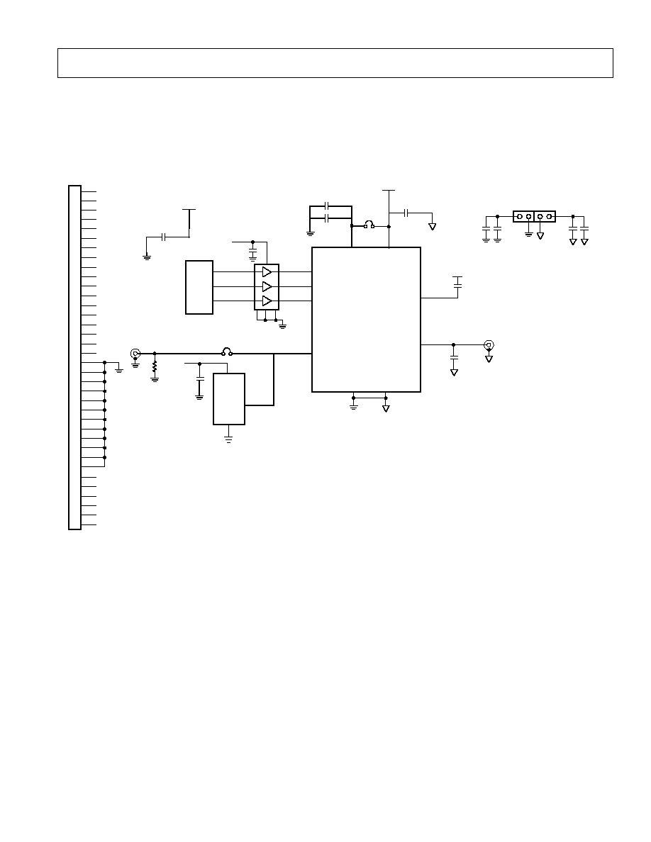
Serial Interface
&
Control Logic
SCLK
SDATA
FSYNC
Control Register
PHASE1 REG
PHASE0 REG
MUX
SIN
ROM
10-Bit DAC
COMP
FullScale
Control
MUX
FREQ0 REG
MCLK
FREQ1 REG
12
On-Board
Reference
AGND
DGND
VDD
AD9833
Phase
Accumulator
(28 Bit)
Regulator
CAP/2.5V
2.5V
AVDD/
DVDD
VOUT
MUX
DIV BY
2
MSB
MUX
R
200
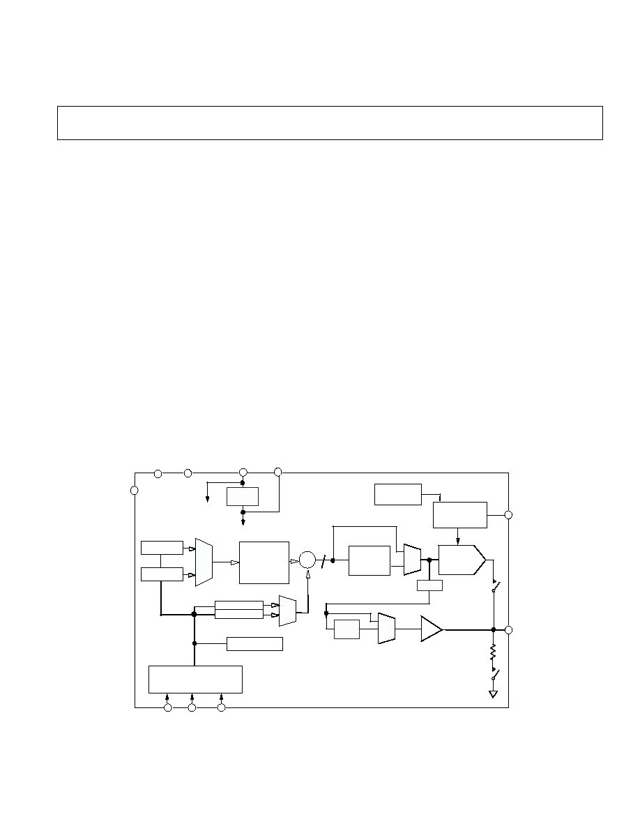
FUNCTIONAL BLOCK DIAGRAM
GENERAL DESCRIPTION
This low power DDS device is a numerically controlled
oscillator employing a phase accumulator, a SIN ROM
and a 10-bit D/A converter integrated on a single
CMOS chip. Clock rates up to 25 MHz are supported
with a power supply from +2.3 V to +5.5 V.
Capability for phase modulation and frequency modula-
tion is provided. Frequency accuracy can be controlled to
one part in 0.25 billion. Modulation is effected by loading
registers through the serial interface.
The AD9833 offers a variety of output waveforms from
the VOUT pin. The SIN ROM can be bypassed so that a
linear up/down ramp is output from the DAC. If the SIN
ROM is not by-passed, a sinusoidal output is available.
Also, if a clock output is required, the MSB of the DAC
data can be output.
The digital section is internally operated at +2.5 V, irre-
spective of the value of VDD, by an on board regulator
which steps down VDD to +2.5 V, when VDD exceeds
+2.5 V.
The AD9833 has a power-down function (SLEEP). This
allows sections of the device which are not being used to
be powered down, thus minimising the current consump-
tion of the part e.g the DAC can be powered down when a
clock output is being generated.
The AD9833 is available in a 10-pin
µ
SOIC package.
PRELIMINARY TECHNICAL DATA
REV PrG 02/02
Information furnished by Analog Devices is believed to be accurate and
reliable. However, no responsibility is assumed by Analog Devices for its
use, nor for any infringements of patents or other rights of third parties
which may result from its use. No license is granted by implication or
otherwise under any patent or patent rights of Analog Devices.
One Technology Way, P.O. Box 9106, Norwood, MA 02062-9106,U.S.A.
Tel: 781/329-4700
www.analog.com
Fax: 781/326-8703
© Analog Devices, Inc., 2002

AD9833
2
REV PrG
PRELIMINARY TECHNICAL DATA
Parameter
Min
Typ
Max
Units
Test Conditions/Comments
SIGNAL DAC SPECIFICATIONS
Resolution
10
Bits
Update Rate (f
MAX
)
25
MSPS
Output Compliance
2
0.8
V
DC Accuracy:
Integral Nonlinearity
±1
LSB
Differential Nonlinearity
±0.5
LSB
DDS SPECIFICATIONS
Dynamic Specifications:
Signal to Noise Ratio
50
dB
f
MCLK
= 25 MHz, f
OUT
= 1.5 kHz
Total Harmonic Distortion
-53
dBc
f
MCLK
= 25 MHz, f
OUT
= 1.5 kHz
Spurious Free Dynamic Range (SFDR):
Wideband (± 2 MHz)
50
dBc
f
MCLK
= 25 MHz, f
OUT
= f
MCLK
/3
55
dBc
f
MCLK
= 25 MHz, f
OUT
= 0.5 MHz
NarrowBand (± 50 kHz)
72
dBc
f
MCLK
= 25 MHz, f
OUT
= f
MCLK
/3
75
dBc
f
MCLK
= 25 MHz, f
OUT
= 0.5 MHz
Clock Feedthrough
55
dBc
Wake Up Time
1
ms
OUTPUT BUFFER
Output Rise/Fall Time
20
ns
Using a 15 pF Load
Output Jitter
100
ps rms
When DAC data MSB is output
VOLTAGE REFERENCE
Internal Reference
1.116
1.2
1.284
V
1.2 V ± 7%
LOGIC INPUTS
V
INH
, Input High Voltage
V
DD
0.9
V
+3.6 V to +5.5 V Power Supply
V
DD
- 0.5
V
+2.7 V to +3.6 V Power Supply
2
V
+2.3 V to + 2.7 V Power Supply
V
INL
, Input Low Voltage
0.9
V
+3.6 V to +5.5 V Power Supply
0.5
V
+2.3 V to + 3.6 V Power Supply
I
INH
, Input Current
1
µA
C
IN
, Input Capacitance
10
pF
POWER SUPPLIES
f
MCLK
= 25 MHz, f
OUT
= f
MCLK
/7
VDD
2.3
5.5
V
I
AA
3
5
mA
I
DD
3
1 + 0.04/MHz
mA
I
AA
+ I
DD
3
7
10
mA
3 V Power Supply
10
15
mA
5 V Power Supply
Low Power Sleep Mode
3
0.25
mA
DAC and Internal Clock Powered Down
NOTES
1
Operating temperature range is as follows: B Version: 40°C to +85°C; typical specifications are at 25 C
2
Guaranteed by Design.
3
Measured with the digital inputs static and equal to 0 V or DVDD.
Specifications subject to change without notice. There is 95% test coverage of the digital circuitry.
SPECIFICATIONS
1
(V
DD
= +2.3 V to +5.5 V; AGND = DGND = 0 V; T
A
= T
MIN
to T
MAX
; R
SET
= 6.8 k
for
VOUT unless otherwise noted)
AD9833
3
REV PrG
PRELIMINARY TECHNICAL DATA
TIMING CHARACTERISTICS
1
(V
DD
= +2.3 V to +5.5 V; AGND = DGND = 0 V, unless otherwise noted)
Parameter
Limit at T
MIN
to T
MAX
Units
Test Conditions/Comments
t
1
40
ns min
MCLK Period
t
2
16
ns min
MCLK High Duration
t
3
16
ns min
MCLK Low Duration
t
4
25
ns min
SCLK Period
t
5
10
ns min
SCLK High Duration
t
6
10
ns min
SCLK Low Duration
t
7
5
ns min
FSYNC
to SCLK Falling Edge Setup Time
t
8
10
ns min
FSYNC to SCLK Hold Time
t
4
- 5
ns max
t
9
5
ns min
Data Setup Time
t
10
3
ns min
Data Hold Time
1
Guaranteed by design, not production tested.
Figure 2. Master Clock
Figure 3. Serial Timing
MCLK
t
2
t
1
t
3
SCLK
FSYNC
SDATA
t
5
t
4
t
6
t
7
t
8
t
10
t
9
D15
D14
D2
D1
D0
D15
D14
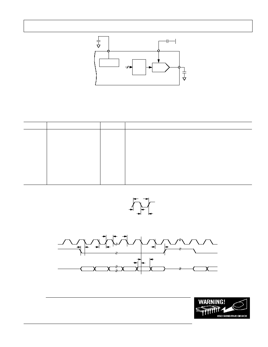
Figure 1. Test Circuit With which Specifications are tested.
VOUT
COMP
12
AD9833
10-BIT DAC
SIN
ROM
20pF
10nF
VDD
REGULATOR
100nF
CAP/2.5V
CAUTION
ESD (electrostatic discharge) sensitive device. Electrostatic charges as high as 4000 V readily
accumulate on the human body and test equipment and can discharge without detection.
Although the AD9833 features proprietary ESD protection circuitry, permanent damage may
occur on devices subjected to high energy electrostatic discharges. Therefore, proper ESD
precautions are recommended to avoid performance degradation or loss of functionality.
AD9833
4
REV PrG
PRELIMINARY TECHNICAL DATA
ABSOLUTE MAXIMUM RATINGS*
(T
A
= +25°C unless otherwise noted)
VDD to AGND . . . . . . . . . . . . . . . . . . . . . 0.3 V to +6 V
VDD to DGND . . . . . . . . . . . . . . . . . . . . . 0.3 V to +6 V
AGND to DGND. . . . . . . . . . . . . . . . . . 0.3 V to +0.3 V
CAP/2.5V . . . . . . . . . . . . . . . . . . . . . . . . . . . . . . . . . . 2.75 V
Digital I/O Voltage to DGND . 0.3 V to VDD + 0.3 V
Analog I/O Voltage to AGND . 0.3 V to VDD + 0.3 V
Operating Temperature Range
Industrial (B Version) . . . . . . . . . . . . . . 40°C to +85°C
Storage Temperature Range . . . . . . . . . 65°C to +150°C
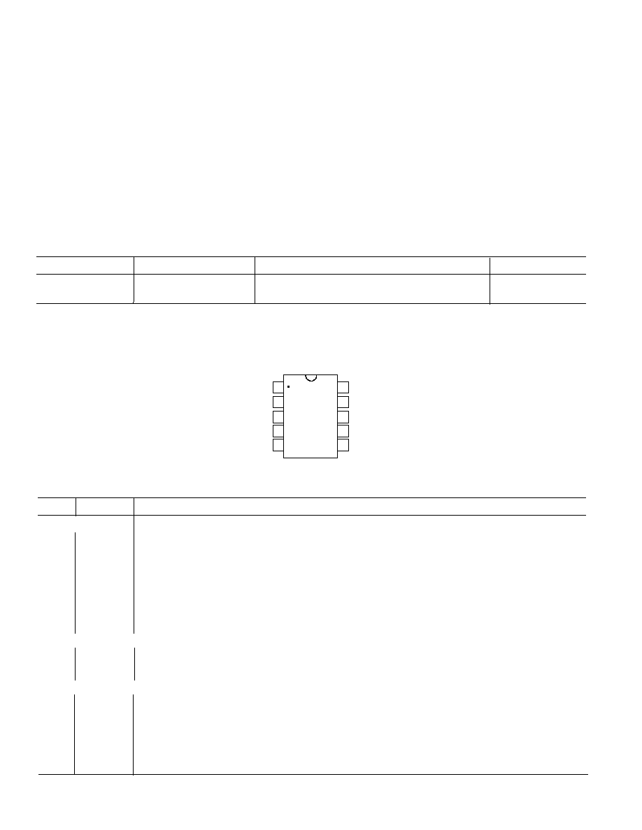
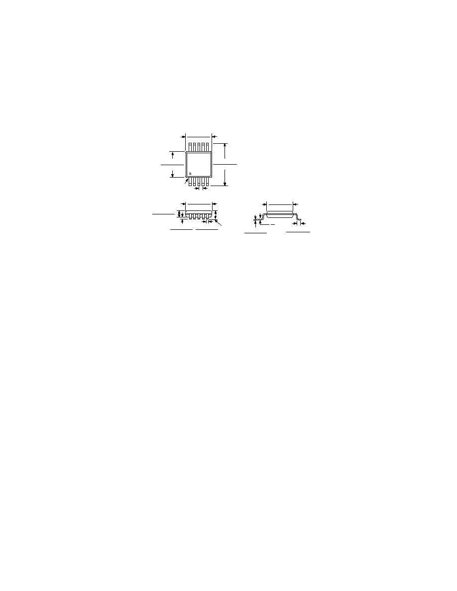
PIN CONFIGURATION
Maximum Junction Temperature . . . . . . . . . . . . . . 150°C
µ
SOIC Package
JA
Thermal Impedance . . . . . . . . . . . . . . . . . . . 206°C/W
JC
Thermal Impedance . . . . . . . . . . . . . . . . . . . 44°C/W
Lead Temperature, Soldering (10 sec) . . . . . . . . . 300°C
IR Reflow, Peak Temperature . . . . . . . . . . . . . . . 220°C
*Stresses above those listed under "Absolute Maximum Ratings" may cause permanent
damage to the device. This is a stress rating only and functional operation of the device
at these or any other conditions above those listed in the operational sections of this
specification is not implied. Exposure to absolute maximum rating conditions for
extended periods may affect device reliability.
ORDERING GUIDE
Model
Temperature Range
Package Description
Package Option
AD9833BRM
40°C to +85°C
14-Pin
µ
SOIC (Micro Small Outline IC )
RM-10
EVAL-AD9833EB
Evaluation Board
1
2
3
4
5
6
7
8
TOP VIEW
(Not to Scale)
VDD
CAP/2.5V
DGND
MCLK
VOUT
AGND
FSYNC
SCLK
SDATA
AD9833
10
9
COMP
PIN DESCRIPTION
Pin #
Mnemonic
Function
POWER SUPPLY
2
V D D
Positive power supply for the analog section and the digital interface sections. The on board 2.5 V
regulator is also supplied from VDD. VDD can have a value from +2.3 V to +5.5 V. A 0.1 µF and
10 µF decoupling capacitor should be connected between VDD and AGND.
3
CAP/2.5V
The digital circuitry operates from a +2.5 V power supply. This +2.5 V is generated from VDD
using an on board regulator (when VDD exceeds +2.7 V). The regulator requires a decoupling
capacitor of typically 100 nF, which is connected from CAP/2.5V to DGND. If VDD is equal to
or less than +2.7 V, CAP/2.5V should be tied directly to VDD.
4
D G N D
Digital Ground.
9
A G N D
Analog Ground.
ANALOG SIGNAL AND REFERENCE
1
C O M P
A DAC Bias Pin. This pin is used for de-coupling the DAC bias voltage.
10
V O U T
Voltage Output. The analog and digital output from the AD9833 is available at this pin. An
external load resistor is not required as the device has a 200W resistor on board.
DIGITAL INTERFACE AND CONTROL
5
MCLK
Digital Clock Input. DDS output frequencies are expressed as a binary fraction of the frequency of
MCLK. The output frequency accuracy and phase noise are determined by this clock.
6
SDATA
Serial Data Input. The 16-bit serial data word is applied to this input.
7
SCLK
Serial Clock Input. Data is clocked into the AD9833 on each falling SCLK edge.
8
F S Y N C
Active Low Control Input. This is the frame synchronisation signal for the input data. When
FSYNC is taken low, the internal logic is informed that a new word is being loaded into the
device.

AD9833
5
REV PrG
PRELIMINARY TECHNICAL DATA
Typical Performance Characteristics
T B D
TPC 1. Typical Current Consumption
vs. MCLK Frequency
T B D
TPC 4. Wide Band SFDR vs. f
OUT
/f
MCLK
for Various MCLK Frequencies
T B D
TPC 7. Wake-Up Time vs.
Temperature
T B D
TPC 2. Narrow Band SFDR vs. MCLK
Frequency
T B D
TPC 5. SNR vs. MCLK Frequency
T B D
TPC 3. Wide Band SFDR vs. MCLK
Frequency
T B D
TPC 6. SNR vs. f
OUT
/f
MCLK
for
Various MCLK Frequencies

AD9833
6
REV PrG
PRELIMINARY TECHNICAL DATA
Typical Performance Characteristics
T B D
TPC 9. f
MCLK
= 10 MHz; f
OUT
= 2.4 kHz;
Frequency Word = 000FBA9
T B D
TPC 12. f
MCLK
= 25 MHz; f
OUT
= 6 kHz;
Frequency Word = 000FBA9
T B D
TPC 15. f
MCLK
= 25 MHz;
f
OUT
= 2.4 MHz;
Frequency Word = 189374D
T B D
TPC 10. f
MCLK
= 10 MHz; f
OUT
= 1.43 kHz
= f
MCLK
/7 ;
Frequency Word = 2492492
T B D
TPC 13. f
MCLK
= 25 MHz; f
OUT
= 60 kHz;
Frequency Word = 009D495
T B D
TPC 16. f
MCLK
= 25 MHz;
f
OUT
= 3.857 MHz = f
MCLK
/7 ;
Frequency Word = 277EE4F
T B D
TPC 11. f
MCLK
= 10 MHz; f
OUT
= 3.33 kHz
= f
MCLK
/3 ;
Frequency Word = 5555555
T B D
TPC 14. f
MCLK
= 25 MHz; f
OUT
= 600 kHz;
Frequency Word = 0624DD3
T B D
TPC 17. f
MCLK
= 25 MHz;
f
OUT
= 8.333 MHz = f
MCLK
/3 ;
Frequency Word = 555475C
AD9833
7
REV PrG
PRELIMINARY TECHNICAL DATA
TERMINOLOGY
Integral Nonlinearity
This is the maximum deviation of any code from a
straight line passing through the endpoints of the transfer
function. The endpoints of the transfer function are zero
scale, a point 0.5 LSB below the first code transition
(000 . . . 00 to 000 . . . 01) and full scale, a point 0.5 LSB
above the last code transition (111 . . . 10 to 111 . . . 11).
The error is expressed in LSBs.
Differential Nonlinearity
This is the difference between the measured and ideal 1
LSB change between two adjacent codes in the DAC. A
specified differential nonlinearity of
±1 LSB maximium ensures
monotonicity.
Output Compliance
The output compliance refers to the maximum voltage
that can be generated at the output of the DAC to meet
the specifications. When voltages greater than that speci-
fied for the output compliance are generated, the AD9833
may not meet the specifications listed in the data sheet.
Spurious Free Dynamic Range
Along with the frequency of interest, harmonics of the
fundamental frequency and images of the these frequencies
are present at the output of a DDS device. The spurious
free dynamic range (SFDR) refers to the largest spur or
harmonic which is present in the band of interest. The
wide band SFDR gives the magnitude of the largest har-
monic or spur relative to the magnitude of the fundamental
frequency in the 0 to Nyquist bandwidth. The narrow band
SFDR gives the attenuation of the largest spur or harmonic
in a bandwidth of ±200 kHz about the fundamental fre-
quency.
Total Harmonic Distortion
Total Harmonic Distortion (THD) is the ratio of the rms
sum of harmonics to the rms value of the fundameltal. For
the AD9834, THD is defined as:
THD = 20 log
(
V
2
2
+ V
3
2
+ V
4
2
+ V
5
2
+ V
6
2
)/V
1
where V
1
is the rms amplitude of the fundamental and V
2
,
V
3
, V
4
, V
5
and V
6
are the rms amplitudes of the second
through thre sixth harmonic.
Signal-to-Noise Ratio (SNR)
S/N is the ratio of the rms value of the measured output
signal to the rms sum of all other spectral components
below the Nyquist frequency, excluding the first six har-
monics and dc. The value for SNR is expressed in
decibels.
Clock Feedthrough
There will be feedthrough from the MCLK input to the
analog output. Clock feedthrough refers to the magnitude
of the MCLK signal relative to the fundamental frequency
in the AD9834's output spectrum.
THEORY OF OPERATION
Sine waves are typically thought of in terms of their
magnitude form a(t) = sin (
t). However, these are
nonlinear and not easy to generate except through piece
wise construction. On the other hand, the angular
information is linear in nature. That is, the phase angle
rotates through a fixed angle for each unit of time. The
angular rate depends on the frequency of the signal by the
traditional rate of
= 2
f.
Figure 4. Sine Wave
Knowing that the phase of a sine wave is linear and given
a reference interval (clock period), the phase rotation for
that period can be determined.
Phase =
t
Solving for
=
Phase/
t = 2
f
Solving for f and substituting the reference clock
frequency for the reference period (1/f
MCLK
=
t)
f =
Phase x f
MCLK
/2
The AD9833 builds the output based on this simple
equation. A simple DDS chip can implement this
equation with three major subcircuits:
Numerical Controlled Oscillator + Phase Modulator
SIN ROM
Digital- to- Analog Convertor.
Each of these sub-circuits are discussed in the following
section.
MAGNITUDE
PHASE
+1
0
- 1
2
0

AD9833
8
REV PrG
PRELIMINARY TECHNICAL DATA
CIRCUIT DESCRIPTION
The AD9833 is a fully integrated Direct Digital Synthesis
(DDS) chip. The chip requires one reference clock, one
low precision resistor and decoupling capacitors to pro-
vide digitally created sine waves up to 12.5 MHz. In
addition to the generation of this RF signal, the chip is
fully capable of a broad range of simple and complex
modulation schemes. These modulation schemes are fully
implemented in the digital domain allowing accurate and
simple realization of complex modulation algorithms us-
ing DSP techniques.
The internal circuitry of the AD9833 consists of the fol-
lowing main sections: a Numerical Controlled Oscillator
(NCO), Frequency and Phase Modulators, SIN ROM, a
Digital-to-Analog Converter, and a Regulator.
Numerical Controlled Oscillator + Phase Modulator
This consists of two frequency select registers, a phase
accumulator, two phase offset registers and a phase offset
adder. The main component of the NCO is a 28-bit phase
accumulator which assembles the phase component of the
output signal. Continuous time signals have a phase range
of 0 to 2 . Outside this range of numbers, the sinusoid
functions repeat themselves in a periodic manner. The
digital implementation is no different. The accumulator
simply scales the range of phase numbers into a multibit
digital word. The phase accumulator in the AD9833 is
implemented with 28 bits. Therefore, in the AD9833, 2
= 2
28
. Likewise, the
Phase term is scaled into this range
of numbers 0 <
Phase < 2
28
1. Making these substitu-
tions into the equation above
f =
Phase x f
MCLK
/2
28
where 0 <
Phase < 2
28
- 1.
The input to the phase accumulator (i.e., the phase step)
can be selected either from the FREQ0 Register or
FREQ1 Register and this is controlled by the FSELECT
bit. NCOs inherently generate continuous phase signals,
thus avoiding any output discontinuity when switching
between frequencies.
Following the NCO, a phase offset can be added to
perform phase modulation using the 12-bit Phase
Registers. The contents of one of these phase registers is
added to the most significant bits of the NCO. The
AD9833 has two Phase registers, the resolution of these
registers being 2
/4096.
SIN ROM
To make the output from the NCO useful, it must be
converted from phase information into a sinusoidal value.
Since phase information maps directly into amplitude, the
SIN ROM uses the digital phase information as an ad-
dress to a look-up table, and converts the phase
information into amplitude. Although the NCO contains a
28-bit phase accumulator, the output of the NCO is trun-
cated to 12 bits. Using the full resolution of the phase
accumulator is impractical and unnecessary as this would
require a look-up table of 2
28
entries. It is necessary only
to have sufficient phase resolution such that the errors due
to truncation are smaller than the resolution of the 10-bit
DAC. This requires the SIN ROM to have two bits of
phase resolution more than the 10-bit DAC.
The SIN ROM is enabled using the MODE bit (D1) in
the control register. This is explained further in Table 11.
Digital-to-Analog Converter
The AD9833 includes a high impedance current source
10-bit DAC. The DAC receives the digital words from
the SIN ROM and converts them into the corresponding
analog voltages.
The DAC is configured for single-ended operation. An
external load resistor is not required as the device has a
200
resistor on board. The DAC generates an output
voltage of typically 0.6 Vpp.
Regulator
VDD provides the power supply required for the analog
section and the digital section of the AD9833. This supply
can have a value of +2.3V to +5.5V
The internal digital section of the AD9833 is operated at
2.5 V. An on-board regulator steps down the voltage ap-
plied at VDD to 2.5 V. When the applied voltage at the
VDD pin of the AD9833 is equal to or less than 2.7 V,
the pins CAP/2.5V and VDD should be tied together, thus
by-passing the on-board regulator.
AD9833
9
REV PrG
PRELIMINARY TECHNICAL DATA
FUNCTIONAL DESCRIPTION
Serial Interface
The AD9833 has a standard 3-wire serial interface, which
is compatible with SPI, QSPI, MICROWIRE and DSP
interface standards.
Data is loaded into the device as a 16-bit word under the
control of a serial clock input, SCLK. The timing dia-
gram for this operation is given in Figure 3.
The FSYNC input is a level triggered input that acts as a
frame synchronisation and chip enable. Data can only be
transferred into the device when FSYNC is low. To start
the serial data transfer, FSYNC should be taken low, ob-
serving the minimum FSYNC to SCLK falling edge setup
time, t
7
. After FSYNC goes low, serial data will be shifted
into the device's input shift register on the falling edges of
SCLK for 16 clock pulses. FSYNC may be taken high
after the sixteenth falling edge of SCLK, observing the
minimum SCLK falling edge to FSYNC rising edge time,
t
8
. Alternatively, FSYNC can be kept low for a multiple of
16 SCLK pulses, and then brought high at the end of the
data transfer. In this way, a continuous stream of 16 bit
words can be loaded while FSYNC is held low, FSYNC
only going high after the 16th SCLK falling edge of the
last word loaded.
The SCLK can be continuous or, alternatively, the SCLK
can idle high or low between write operations.
Powering up the AD9833
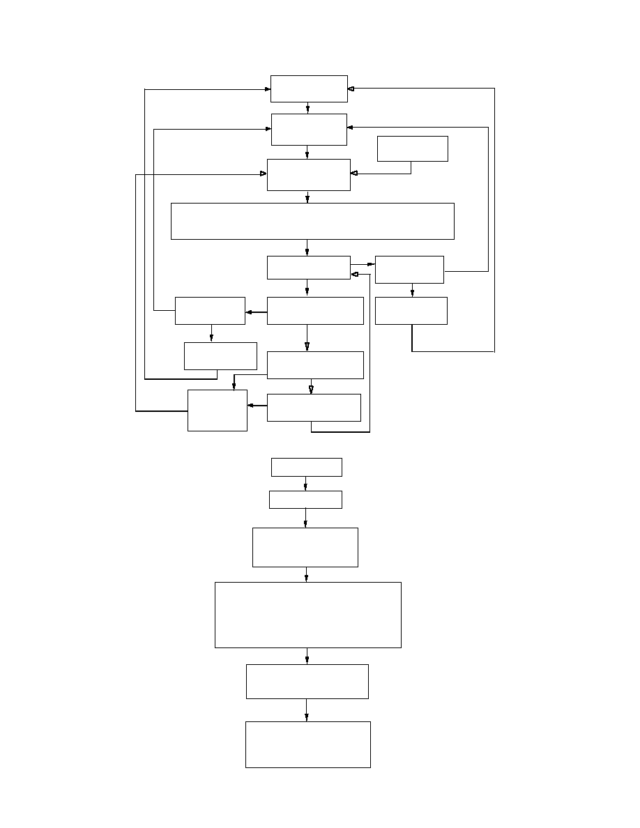
The flow chart in Figure 6 shows the operating routine for
the AD9833. When the AD9833 is powered up, the part
should be reset. This will reset appropriate internal regis-
ters to zero to provide an analog output of midscale. To
avoid spurious DAC outputs while the AD9833 is being
initialized, the RESET bit should be set to 1 until the part
is ready to begin generating an output. RESET does not
reset the phase, frequency or control registers. These reg-
isters will contain invalid data and, therefore, should be set
to a known value by the user. The RESET bit should then
be set to 0 to begin generating an output. A signal will
appear at the DAC output 7 MCLK cycles after RESET is
set to 0.
Latency
Associated with each asynchronous write operation in the
AD9833 is a latency. If a selected frequency/phase register
is loaded with a new word there is a delay of 7 to 8 MCLK
cycles before the analog output will change. (There is an
uncertainty of one MCLK cycle as it depends on the posi-
tion of the MCLK rising edge when the data is loaded into
the destination register.)
The Control Register
The AD9833 contains a 16-bit control register which sets
up the AD9833 as the user wishes to operate it. All control
bits, except MODE, are sampled on the internal negative
edge of MCLK.
Table 2, on the following page, describes the individual
bits of the control register. The different functions and the
various output options from the AD9833 are described in
more detail in the section following Table 2.
To inform the AD9833 that you wish to alter the contents
of the Control register, D15 and D14 must be set to '0' as
shown below.
Table 1. Control Register
D15
D14
D13
D0
0
0
CONTROL BITS
Figure 5. Function of Control Bits
S IN
R O M
(L ow P ow er)
10-Bit DA C
V O U T
A D 9833
P hase
A ccu m u lator
(28 B it)
M U X
D IV B Y
2
M U X
D IG IT AL
O U TP U T
(enab le)
S L EE P 12
S LE E P 1
R E S E T
O P B IT EN
D IV 2
0
1
1
0
DB15 DB14
DB13
DB12 DB11
DB10
DB9
DB8
DB7
DB6
DB5
DB4
DB3
DB2
DB1
DB0
0
0
B2 8
HLB
FSELECT PSELECT
0
RESET
SLEEP1 SLEEP12
O PBITEN
0
DIV2
0
M ODE
0
M O D E + O P BITE N

AD9833
10
REV PrG
PRELIMINARY TECHNICAL DATA
Table 2. Description of bits in the Control Register
Bit
Name
Function
D13
B28
Two write operations are required to load a complete word into either of the Frequency registers.
B28 = '1' allows a complete word to be loaded into a frequency register in two consecutive
writes. The first write contains the 14 LSBs of the frequency word and the next write will
contain the 14 MSBs. The first two bits of each sixteen-bit word define the frequency register to
which the word is loaded, and should therefore be the same for both of the consecutive writes.
Refer to table 6 for the appropriate addresses. The write to the frequency register occurs after both
words have been loaded, so the register never holds an intermediate value. An example of a com-
plete 28-bit write is shown in table 5.
When B28 = '0' the 28-bit frequency register operates as 2 14-bit registers, one containing the 14
MSBs and the other containing the 14 LSBs. This means that the 14 MSBs of the frequency
word can be altered independent of the 14 LSBs and vice versa. To alter the 14 MSBs or the 14
LSBs, a single write is made to the appropriate Frequency address. The control bit D12 (HLB)
informs the AD9833 whether the bits to be altered are the 14 MSBs or 14 LSBs.
D12
H L B
This control bit allows the user to continuously load the MSBs or LSBs of a frequency register
while ignoring the remaining 14 bits. This is useful if the complete 28 bit resolution is not re-
quired. HLB is used in conjunction with D13 (B28). This control bit indicates whether the 14 bits
being loaded are being transferred to the 14 MSBs or 14 LSBs of the addressed frequency regis-
ter. D13 (B28) must be set to '0' to be able to change the MSBs and LSBs of a frequency word
seperately. When D13 (B28) = '1', this control bit is ignored.
HLB = '1' allows a write to the 14 MSBs of the addressed frequency register.
HLB = '0' allows a write to the 14 LSBs of the addressed frequency register.
D11
F S E L E C T
The FSELECT bit defines whether the FREQ0 register or the FREQ1 register is used in the
phase accumulator.
D10
P S E L E C T
The PSELECT bit defines whether the PHASE0 register or the PHASE1 register data is added to
the output of the phase accumulator.
D 9
Reserved
This bit should be set to 0.
D 8
R E S E T
RESET = '1' resets internal registers to zero, which corresponds to an analog output of midscale.
RESET = '0' disables Reset. This function is explained further in Table 9.
D 7
S L E E P 1
When SLEEP1 = '1', the internal MCLK clock is disabled. The DAC output will remain at its
present value as the NCO is no longer accumulating.
When SLEEP1 = '0' MCLK is enabled. This function is explained further in Table 10.
D 6
SLEEP12
SLEEP12 = '1' powers down the on-chip DAC. This is useful when the AD9833 is used to output
the MSB of the DAC data.
SLEEP12 = '0' implies that the DAC is active. This function is explained further in Table 10.
D 5
O P B I T E N
The function of this bit, in association with D1 (MODE), is to control what is output at the
VOUT pin. This is explained further in Table 11.
When OPBITEN = '1' the output of the DAC is no longer available at the VOUT pin. Instead,
the MSB (or MSB/2) of the DAC data is connected to the VOUT pin. This is useful as a coarse
clock source. The bit DIV2 controls whether it is the MSB or MSB/2 that is ouput.
When OPBITEN equals 0, the DAC is connected to VOUT. The MODE bit determines whether
it is a sinusoidal or a ramp output that is available.
D 4
Reserved
This bit must be set to 0.
D 3
DIV2
DIV2 is used in association with D5 (OPBITEN). This is explained further in Table 11.
When DIV2 = '1', the MSB of the DAC data is passed directly to the VOUT pin.
When DIV2 = '0', the MSB/2 of the DAC data is output at the VOUT pin.
D 2
Reserved
This bit must always be set to 0.
D 1
M O D E
This bit is used in association with OPBITEN (D5). The function of this bit is to control what is
output at the VOUT pin when the on-chip DAC is connected to VOUT. This bit should be
set to '0' if the control bit OPBITEN = '1'. This is explained further in Table 11.
When MODE = '1', the SIN ROM is bypassed, resulting in a ramp output from the DAC.
When MODE = '0' the SIN ROM is used to convert the phase information into amplitude infor-
mation which results in a sinusoidal signal at the output.
D 0
Reserved
This bit must always be set to 0.
AD9833
11
REV PrG
PRELIMINARY TECHNICAL DATA
The Frequency and Phase Resisters
The AD9833 contains 2 frequency registers and 2 phase
registers. These are described in Table 3 below.
Table 3. Frequency/Phase Registers
Register
Size
Description
F R E Q 0
28 Bits Frequency Register 0. When the
F S E L E C T bit = 0, this register
defines the output frequency as a
fraction of the MCLK frequency.
F R E Q 1
28 Bits Frequency Register 1. When the
F S E L E C T bit = 1, this register
defines the output frequency as a
fraction of the MCLK frequency.
PHASE0
12 Bits Phase Offset Register 0. When the
PSELECT bit = 0, the contents of
this register are added to the output
of the phase accumulator.
PHASE1
12 Bits Phase Offset Register 1. When the
PSELECT bit = 1, the contents of
this register are added to the output
of the phase accumulator.
The analog output from the AD9833 is
f
MCLK
/2
28
x FREQREG
where FREQREG is the value loaded into the selected
frequency register. This signal will be phase shifted by
2
/4096 x PHASEREG
where PHASEREG is the value contained in the selected
phase register.
The flow chart in Figure 8 shows the routine for writing
to the frequency and phase registers of the AD9833.
Writing to a Frequency Register:
When writing to a frequency register, bits D15 and D14
give the address of the frequency register.
Table 4. Frequency Register Bits
D15
D14
D13
D 0
0
1
MSB
14 FREQ0 REG BITS
LSB
1
0
MSB
14 FREQ1 REG BITS
LSB
If the user wishes to alter the entire contents of a fre-
quency register, two consecutive writes to the same
address must be performed, as the frequency registers are
28 bits wide. The first write will contain the 14 LSBs
while the second write will contain the 14 MSBs. For this
mode of operation, the control bit B28 (D13) should be
set to 1. An example of a 28-bit write is shown in Table 5.
Table 5: Writing 3FFF0000 to FREQ0 REG
SDATA input
Result of input word
0010 0000 0000 0000
Control word write (D15, D14 = 00);
B28 (D13) = 1; HLB (D12) = X
0100 0000 0000 0000
FREQ0 REG write (D15, D14 = 01);
14 LSBs = 0000
0111 1111 1111 1111
FREQ0 REG write (D15, D14 = 01);
14 MSBs = 3FFF
In some applications, the user does not need to alter all 28
bits of the frequency register. With coarse tuning, only
the 14 MSBs are altered while with fine tuning, only the
14 LSBs are altered. By setting the control bit B28 (D13)
to 0, the 28-bit frequency register operates as 2 14-bit
registers, one containing the 14 MSBs and the other con-
taining the 14 LSBs. This means that the 14 MSBs of the
frequency word can be altered independent of the 14 LSBs
and vice versa. Bit HLB (D12) in the control register
identifies which 14 bits are being altered. Examples of this
are shown below.
Table 6: Writing 3FFF to the 14 LSBs of FREQ1 REG
SDATA input
Result of input word
0000 0000 0000 0000
Control word write (D15, D14 = 00);
B28 (D13) = 0; HLB (D12) = 0, i.e. LSBs
1011 1111 1111 1111
FREQ1 REG write (D15, D14 = 10);
14 LSBs = 3FFF
Table 7: Writing 3FFF to the 14 MSBs of FREQ0 REG
SDATA input
Result of Input word
0001 0000 0000 0000
Control word write (D15, D14 = 00);
B28 (D13) = 0; HLB (D12) = 1, i.e. MSBs
0111 1111 1111 1111
FREQ0 REG write (D15, D14 = 01);
14 MSBs = 3FFF
Writing to a Phase Register:
When writing to a phase register, bits D15 and D14 are
set to 11. Bit D13 identifies which phase register is being
loaded.
Table 8. Phase Register Bits
D15 D14
D13
D12
D11
D 0
1
1
0
X
MSB
12 PHASE0 BITS
LSB
1
1
1
X
MSB
12 PHASE1 BITS
LSB
The RESET Function
The RESET function resets appropriate internal registers
to zero to provide an analog output of midscale. RESET
does not reset the phase, frequency or control registers.
When the AD9833 is powered up, the part should be re-
set. To reset the AD9833, set the RESET bit to 1. To
take the part out of reset, set the bit to 0. A signal will

AD9833
12
REV PrG
PRELIMINARY TECHNICAL DATA
appear at the DAC output 7 MCLK cycles after RESET is
set to 0.
Table 9: Applying RESET
RESET bit
Result
0
No Reset Applied
1
Internal Registers Reset
The Sleep Function
Sections of the AD9833 which are not in use can be pow-
ered down to minimise power consumption. This is done
using the Sleep Function. The parts of the chip that can
be powered down are the Internal clock and the DAC.
The bits required for the Sleep Function are outlined in
Table 10.
Table 10: Applying the SLEEP Function
SLEEP1
SLEEP12
Result
bit
bit
0
0
No powerdown
0
1
DAC Powered Down
1
0
Internal Clock disabled
1
1
Both the DAC powered down and
the Internal Clock disabled
DAC Powered Down: This is useful when the AD9833 is
used to output the MSB of the DAC data only. In this
case, the DAC is not required so it can be powered down
to reduce power consumption.
Internal Clock disabled: When the internal clock of the
AD9833 is disabled the DAC output will remain at its
present value as the NCO is no longer accumulating. New
frequency, phase and control words can be written to the
part when the SLEEP1 control bit is active. The
synchronising clock is still active which means that the
selected frequency and phase registers can also be changed
using the control bits. Setting the SLEEP1 bit equal to 0
enables the MCLK. Any changes made to the registers
while SLEEP1 was active will be seen at the output after a
certain latency.
The VOUT Pin
The AD9833 offers a variety of outputs from the chip, all
of which are available from the VOUT pin. The choice of
outputs are:
The MSB of the DAC data,
A sinusoidal output or
A ramp output.
The bits OPBITEN (D5) and MODE (D1) in the control
register are used to decide which output is available from
the AD9833. This is explained further below and also in
Table 11.
MSB of the DAC data: The MSB of the DAC data can be
output from the AD9833. By setting the OPBITEN (D5)
control bit to 1, the MSB of the DAC data is available at
the VOUT pin. This is useful as a coarse clock source.
This square wave can also be divided by 2 before being
output. The bit DIV2 (D3) in the control register controls
the frequency of this output from the VOUT pin.
Sinusoidal Output: The SIN ROM is used to convert the
phase information from the frequency and phase registers
into amplitude information which results in a sinusoidal
signal at the output. To have a sinusoidal output from the
VOUT pin, set the bit MODE (D1) = 0 and the
OPBITEN (D5) bit to 0.
Up/Down Ramp Output: The SIN ROM can be bypassed
so that the truncated digital output from the NCO is sent
to the DAC. In this case, the output is no longer sinusoi-
dal. The DAC will produce a ramp up/down function. To
have a ramp output from the VOUT pin set the bit
MODE (D1) = 1.
Note that the SLEEP12 bit must be 0 (i.e. the DAC is
enabled) when using this pin.
Table 11: Various Outputs from VOUT
OPBITEN
MODE
DIV2
VOUT
bit
bit
bit
Pin
0
0
X
Sinusoid
0
1
X
Up/Down Ramp
1
0
0
DAC data MSB / 2
1
0
1
DAC data MSB
1
1
X
Reserved

AD9833
13
REV PrG
PRELIMINARY TECHNICAL DATA
APPLICATIONS
Because of the various output options available from the
part, the AD9833 can be configured to suit a wide variety
of applications.
One of the areas where the AD9833 is suitable is in modu-
lation applications. The part can be used to perform
simple modulation such as FSK. More complex modula-
tion schemes such as GMSK and QPSK can also be
implemented using the AD9833.
In an FSK application, the two frequency registers of the
AD9833 are loaded with different values; one frequency
will represent the space frequency while the other will
represent the mark frequency. Using the FSELECT bit in
the control register of the AD9833, the user can modulate
the carrier frequency between the two values.
The AD9833 has two phase registers; this enables the part
to perform PSK. With phase shift keying, the carrier fre-
quency is phase shifted, the phase being altered by an
amount which is related to the bit stream being input to
the modulator.
The AD9833 is also suitable for signal generator applica-
tions. Because the MSB of the DAC data is available at
the VOUT pin, the device can be used to generate a
square wave.
With its low current consumption, the part is suitable for
applications in which it can be used as a local oscillator.
GROUNDING AND LAYOUT
The printed circuit board that houses the AD9833 should
be designed so that the analog and digital sections are
separated and confined to certain areas of the board. This
facilitates the use of ground planes which can be separated
easily. A minimum etch technique is generally best for
ground planes as it gives the best shielding. Digital and
analog ground planes should only be joined in one place.
If the AD9833 is the only device requiring an AGND to
DGND connection, then the ground planes should be
connected at the AGND and DGND pins of the AD9833.
If the AD9833 is in a system where multiple devices re-
quire AGND to DGND connections, the connection
should be made at one point only, a star ground point that
should be established as close as possible to the AD9833.
Avoid running digital lines under the device as these will
couple noise onto the die. The analog ground plane should
be allowed to run under the AD9833 to avoid noise cou-
pling. The power supply lines to the AD9833 should use
as large a track as is possible to provide low impedance
paths and reduce the effects of glitches on the power sup-
ply line. Fast switching signals such as clocks should be
shielded with digital ground to avoid radiating noise to
other sections of the board. Avoid crossover of digital and
analog signals. Traces on opposite sides of the board
should run at right angles to each other. This will reduce
the effects of feedthrough through the board. A microstrip
technique is by far the best but is not always possible with
a double-sided board. In this technique, the component
side of the board is dedicated to ground planes while sig-
nals are placed on the other side.
Good decoupling is important. The AD9833 should have
supply bypassing of 0.1 µF ceramic capacitors in parallel
with 10 µF tantalum capacitors. To achieve the best from
the decoupling capacitors, they should be placed as close
as possible to the device, ideally right up against the de-
vice.
AD9833
14
REV PrG
PRELIMINARY TECHNICAL DATA
Figure 7. Initialisation
Figure 6. Flow Chart for AD9833 Initialisation and Operation
WAIT 7/8 MCLK
CYCLES
VOUT = VREF * 18 * RLOAD/RSET * (1+ (SIN(2
p
(FREQREG * FMCLK * t/2
28 + PHASEREG/212)))
DAC OUTPUT
DATA WRITE
SELECT DATA
SOURCES
INITIALISATION
See Figure 7 below
CHANGE PHASE?
CHANGE FREQUENCY?
CHANGE
FSELECT?
CHANGE FREQ
REGISTER?
CHANGE DAC OUTPUT
FROM SIN TO RAMP?
CONTROL
REGISTER
WRITE
(see Table 11)
CHANGE OUTPUT TO
A DIGITAL SIGNAL?
CHANGE
PSELECT?
CHANGE PHASE
REGISTER?
See Figure 8 below
NO
NO
NO
NO
NO
YES
YES
YES
YES
YES
YES
YES
NO
YES
INITIALISATION
APPLY RESET
WRITE TO FREQUENCY AND PHASE REGISTERS
FREQ0 REG = FOUT0 / fMCLK * 2
28
FREQ1 REG = FOUT1 / fMCLK * 2
28
PHASE 0 & PHASE1 REG = (PhaseShift * 212) / 2
p
(See Figure 8)
SET RESET = 0
SELECT FREQUENCY REGISTERS
SELECT PHASE REGISTERS
(CONTROL REGISTER WRITE)
RESET bit = 0
FSELECT = Selected Freq Register
PSELECT = Selected Phase Register
(CONTROL REGISTER WRITE)
RESET = 1
AD9833
15
REV PrG
PRELIMINARY TECHNICAL DATA
Figure 8. Data Writes
INTERFACING TO MICROPROCESSORS
The AD9833 has a standard serial interface which allows
the part to interface directly with several microprocessors.
The device uses an external serial clock to write the data/
control information into the device. The serial clock can
have a frequency of 40 MHz maximum. The serial clock
can be continuous or, it can idle high or low between
write operations. When data/control information is being
written to the AD9833, FSYNC is taken low and is held
low while the 16 bits of data are being written into the
AD9833. The FSYNC signal frames the 16 bits of infor-
mation being loaded into the AD9833.
AD9833 to ADSP-21xx Interface
Figure 9 shows the serial interface between the AD9833
and the ADSP-21xx. The ADSP-21xx should be set up to
operate in the SPORT Transmit Alternate Framing Mode
(TFSW = 1). The ADSP-21xx is programmed through
the SPORT control register and should be configured as
follows:
Internal clock operation (ISCLK = 1)
Active low framing (INVTFS = 1)
16-bit word length (SLEN = 15)
Internal frame sync signal (ITFS = 1)
Generate a frame sync for each write (TFSR = 1).
Transmission is initiated by writing a word to the Tx reg-
ister after the SPORT has been enabled. The data is
clocked out on each rising edge of the serial clock and
clocked into the AD9833 on the SCLK falling edge.
ADSP-2101/
ADSP-2103*
AD9833*
TFS
DT
SCLK
FSYNC
* ADDITIONAL PINS OMITTED FOR CLARITY
SDATA
SCLK
Figure 9. ADSP2101/ADSP2103 to AD9833 Interface
AD9833 to 68HC11/68L11 Interface
Figure 10 shows the serial interface between the AD9833
and the 68HC11/68L11 microcontroller. The
microcontroller is configured as the master by setting bit
MSTR in the SPCR to 1 and, this provides a serial clock
on SCK while the MOSI output drives the serial data line
SDATA. Since the microcontroller does not have a dedi-
cated frame sync pin, the FSYNC signal is derived from a
port line (PC7). The set up conditions for correct opera-
tion of the interface are as follows:
DATA WRITE
WRITE A FULL 28-BIT WORD
TO A FREQUENCY REGISTER?
WRITE 14 MSBs OR LSBs
TO A FREQUENCY REGISTER?
WRITE TO PHASE
REGISTER?
(CONTROL REGISTER WRITE)
B28 (D13) = 1
WRITE 2 CONSECUTIVE
16-BIT WORDS
(See Table 5 for Example)
WRITE A 16-BIT WORD
(See Tables 6 & 7 for
examples)
(CONTROL REGISTER WRITE)
B28 (D13) = 0
HLB (D12) = 0 / 1
WRITE ANOTHER FULL
28 BITS TO A
FREQUENCY REGISTER?
WRITE 14 MSBs OR LSBs
TO A
FREQUENCY REGISTER?
(16 - Bit Write)
D15, D14 = 11
D13 = 0/1 (chooses the
phase register)
D12 = X
D11 ... D0 = Phase Data
WRITE TO ANOTHER
PHASE REGISTER?
YES
YES
YES
YES
YES
YES
NO
NO
NO
NO
NO
AD9833
16
REV PrG
PRELIMINARY TECHNICAL DATA
SCK idles high between write operations (CPOL = 0)
data is valid on the SCK falling edge (CPHA = 1).
When data is being transmitted to the AD9833, the
FSYNC line is taken low (PC7). Serial data from the
68HC11/68L11 is transmitted in 8-bit bytes with only 8
falling clock edges occuring in the transmit cycle. Data is
transmitted MSB first. In order to load data into the
AD9833, PC7 is held low after the first 8 bits are trans-
ferred and a second serial write operation is performed to
the AD9833. Only after the second 8 bits have been trans-
ferred should FSYNC be taken high again.
68HC11/68L11*
AD9833*
PC7
MOSI
SCK
SDATA
SCLK
FSYNC
* ADDITIONAL PINS OMITTED FOR CLARITY
Figure 10. 68HC11/68L11 to AD9833 Interface
AD9833 to 80C51/80L51 Interface
Figure 11 shows the serial interface between the AD9833
and the 80C51/80L51 microcontroller. The
microcontroller is operated in mode 0 so that TXD of the
80C51/80L51 drives SCLK of the AD9833 while RXD
drives the serial data line SDATA. The FSYNC signal is
again derived from a bit programmable pin on the port
(P3.3 being used in the diagram). When data is to be
transmitted to the AD9833, P3.3 is taken low. The
80C51/80L51 transmits data in 8 bit bytes thus, only 8
falling SCLK edges occur in each cycle. To load the re-
maining 8 bits to the AD9833, P3.3 is held low after the
first 8 bits have been transmitted and a second write op-
eration is initiated to transmit the second byte of data.
P3.3 is taken high following the completion of the second
write operation. SCLK should idle high between the two
write operations. The 80C51/80L51 outputs the serial
data in a format which has the LSB first. The AD9833
accepts the MSB first (the 4 MSBs being the control in-
formation, the next 4 bits being the address while the 8
LSBs contain the data when writing to a destination regis-
ter). Therefore, the transmit routine of the 80C51/80L51
must take this into account and re-arrange the bits so that
the MSB is output first.
80C51/80L51*
AD9833*
P3.3
RXD
TXD
SDATA
SCLK
FSYNC
* ADDITIONAL PINS OMITTED FOR CLARITY
Figure 11. 80C51/80L51 to AD9833 Interface
AD9833 to DSP56002 Interface
Figure 12 shows the interface between the AD9833 and
the DSP56002. The DSP56002 is configured for normal
mode asynchronous operation with a Gated internal clock
(SYN = 0, GCK = 1, SCKD = 1). The frame sync pin is
generated internally (SC2 = 1), the transfers are 16 bits
wide (WL1 = 1, WL0 = 0) and the frame sync signal will
frame the 16 bits (FSL = 0). The frame sync signal is
available on pin SC2 but, it needs to be inverted before
being applied to the AD9833. The interface to the
DSP56000/DSP56001 is similar to that of the DSP56002.
DSP56002*
AD9833*
SC2
STD
SCK
SDATA
SCLK
FSYNC
* ADDITIONAL PINS OMITTED FOR CLARITY
Figure 12. AD9833 to DSP56002 Interface
AD9833 EVALUATION BOARD
The AD9833 Evaluation Board allows designers to evalu-
ate the high performance AD9833 DDS modulator with
minimum of effort.
To prove that this device will meet the user's waveform
synthesis requirements, the user only require's a power-
supply, an IBM-compatible PC and a spectrum analyser
along with the evaluation board.
The DDS evaluation kit includes a populated, tested
AD9833 printed circuit board. The evaluation board in-
terfaces to the parallel port of an IBM compatible PC.
Software is available with the evaluation board which al-
lows the user to easily program the AD9833. A schematic
of the Evaluation board is shown in Figure 13. The soft-
ware will run on any IBM compatible PC which has
Microsoft Windows95, Windows98 or Windows ME 2000
NTTM installed.
Using the AD9833 Evaluation Board
The AD9833 Evaluation kit is a test system designed to
simplify the evaluation of the AD9833. An application
note is also available with the evaluation board and gives
full information on operating the evaluation board.
Prototyping Area
An area is available on the evaluation board for the user to
add additional circuits to the evaluation test set. Users
may want to build custom analog filters for the output or
add buffers and operational amplifiers to be used in the
AD9833
17
REV PrG
PRELIMINARY TECHNICAL DATA
final application.
XO vs. External Clock
The AD9833 can operate with master clocks up to 25
MHz. A 25 MHz oscillator is included on the evaluation
board. However, this oscillator can be removed and, if
required, an external CMOS clock connected to the part.
Figure 13. AD9833 Evaluation Board Layout
Integrated Circuits
U 1
AD9833BRU
U 2
74HCT244
U 3
OSC XTAL 25 MHz
Capacitors
C1 C2
100nF Ceramic Capacitor 0805
C5 C6 C7 C9 100nF Ceramic Capacitor
C 3
10nF ceramic Capacitor
C8 C10 C11
10uF Tantalum Capacitor
C 4
Option for extra decoupling capacitor
Resistor
R1
51
Resistor
Links
Lk1 Lk2
2 pin sil header
Sockets
MCLK VOUT
Sub Minature BNC Connector
Connectors
J 1
36-Pin Edge Connector
J2, J3
PCB Mounting Terminal Block
Power Supply
Power to the AD9833 Evaluation Board must be provided
externally through pin connections. The power leads
should be twisted to reduce ground loops.
C8
10
m
F
C7
0.1
m
F
DVDD
J2
J3
C9
0.1
m
F
C10
10
m
F
VDD
C2
0.1
m
F
VDD
2
VDD
1
10
COMP
VOUT
VDD
C3
0.01
m
F
VOUT
DGND
AGND
4
9
5
8
6
7
MCLK
FSYNC
SDATA
SCLK
18
16
14
1
6
4
2
DVDD
C6
0.1
m
F
U2
J1
SCLK
SDATA
FSYNC
MCLK
50R
DGND
DVDD
OUT
DVDD
C5
0.1
m
F
U3
SCLK
SDATA
FSYNC
1
2
3
4
5
6
7
8
9
10
11
12
13
14
15
16
17
18
19
20
21
22
23
24
25
26
27
28
29
30
31
32
33
34
35
36
U1
AD9833
C4
R1
LK2
CAP
LK1
C11
10
m
F
C1
0.1
m
F
3
DVDD
C6
0.1
m
F
AD9833
18
REV PrG
PRELIMINARY TECHNICAL DATA
OUTLINE DIMENSIONS
Dimensions shown in inches and (mm).
10-Lead mSOIC Package
(RM-10)
0.0197 (0.50) BSC
0.122 (3.10)
0.114 (2.90)
1
0
6
5
1
0.199 (5.05)
0.187 (4.75)
PIN 1
0.122 (3.10)
0.114 (2.90)
0.012 (0.30)
0.006 (0.15)
0.037
(0.94)
0.031
(0.78)
SEATING
PLANE
0.120 (3.05)
0.112 (2.85)
0.043 (1.10)
MAX
0.006 (0.15)
0.002 (0.05)
0.028 (0.70)
0.016 (0.40)
0.009 (0.23)
0.005 (0.13)
6o
0
0.120 (3.05)
0.112 (2.85)
o