 | ÐлекÑÑоннÑй компоненÑ: AD9830 | СкаÑаÑÑ:  PDF PDF  ZIP ZIP |
Äîêóìåíòàöèÿ è îïèñàíèÿ www.docs.chipfind.ru
REV. A
Information furnished by Analog Devices is believed to be accurate and
reliable. However, no responsibility is assumed by Analog Devices for its
use, nor for any infringements of patents or other rights of third parties
which may result from its use. No license is granted by implication or
otherwise under any patent or patent rights of Analog Devices.
a
CMOS
Complete DDS
AD9830
© Analog Devices, Inc., 1996
One Technology Way, P.O. Box 9106, Norwood, MA 02062-9106, U.S.A.
Tel: 617/329-4700
Fax: 617/326-8703
FEATURES
+5 V Power Supply
50 MHz Speed
On-Chip SINE Look-Up Table
On-Chip 10-Bit DAC
Parallel Loading
Power-Down Option
72 dB SFDR
250 mW Power Consumption
48-Pin TQFP
APPLICATIONS
DDS Tuning
Digital Demodulation
GENERAL DESCRIPTION
This DDS device is a numerically controlled oscillator em-
ploying a phase accumulator, a sine look-up table and a
10-bit D/A converter integrated on a single CMOS chip.
Modulation capabilities are provided for phase modulation
and frequency modulation.
Clock rates up to 50 MHz are supported. Frequency accu-
racy can be controlled to one part in 4 billion. Modulation
is effected by loading registers through the parallel micro-
processor interface.
A power-down pin allows external control of a power-down
mode. The part is available in a 48-pin TQFP package.
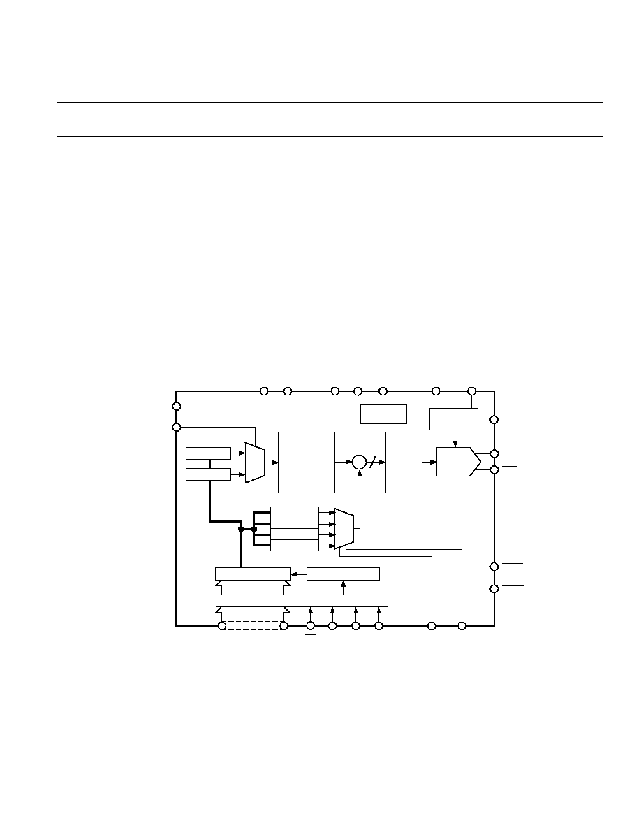
FUNCTIONAL BLOCK DIAGRAM
RESET
SLEEP
IOUT
IOUT
COMP
REFIN
FS ADJUST
REFOUT
AGND
AVDD
DGND
DVDD
MCLK
D0
FSELECT
D15
WR
A0
A1
A2
PSEL0
PSEL1
12
AD9830
ON-BOARD
REFERENCE
FULL SCALE
CONTROL
10-BIT DAC
SIN
ROM
PHASE
ACCUMULATOR
(32-BIT)
MUX
MUX
FREQ0 REG
FREQ1 REG
PHASE0 REG
PHASE1 REG
PHASE2 REG
PHASE3 REG
PARALLEL REGISTER
TRANSFER CONTROL
MPU INTERFACE
REV. A
2
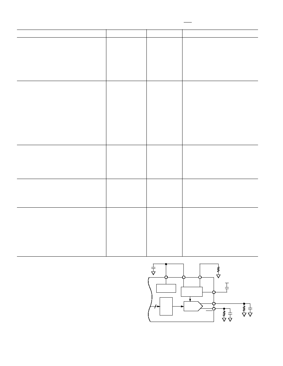
AD9830SPECIFICATIONS
1
Parameter
AD9830A
Units
Test Conditions/Comments
SIGNAL DAC SPECIFICATIONS
Resolution
10
Bits
Update Rate (f
MAX
)
50
MSPS max
I
OUT
Full Scale
20
mA max
Output Compliance
1
V max
DC Accuracy
Integral Nonlinearity
±
1
LSB typ
Differential Nonlinearity
±
0.5
LSB typ
DDS SPECIFICATIONS
2
Dynamic Specifications
Signal-to-Noise Ratio
50
dB min
f
MCLK
= f
MAX
, f
OUT
= 2 MHz
Total Harmonic Distortion
53
dBc max
f
MCLK
= f
MAX
, f
OUT
= 2 MHz
Spurious Free Dynamic Range (SFDR)
3
f
MCLK
= 6.25 MHz, f
OUT
= 2.11 MHz
Narrow Band
(
±
50 kHz)
72
dBc min
(
±
200 kHz)
68
dBc min
Wide Band (
±
2 MHz)
50
dBc min
Clock Feedthrough
55
dBc typ
Wake Up Time
1
ms typ
Power-Down Option
Yes
VOLTAGE REFERENCE
Internal Reference @ +25
°
C
1.21
Volts typ
T
MIN
to T
MAX
1.21
±
7%
Volts min/max
REFIN Input Impedance
10
M
typ
Reference TC
100
ppm/
°
C typ
REFOUT Impedance
300
typ
LOGIC INPUTS
V
INH
, Input High Voltage
V
DD
0.9
V min
V
INL
, Input Low Voltage
0.9
V max
I
INH
, Input Current
10
µ
A max
C
IN
, Input Capacitance
10
pF max
POWER SUPPLIES
f
OUT
= 2 MHz
AVDD
4.75/5.25
V min/V max
DVDD
4.75/5.25
V min/V max
I
AA
25
mA max
I
DD
6 + 0.5/MHz
mA typ
I
AA
+ I
DD
4
60
mA max
Low Power Sleep Mode
5
0.25
mA typ
1 M
Resistor Tied Between
1
mA max
REFOUT and AGND
(V
DD
= +5 V 5%; AGND = DGND = 0 V; T
A
= T
MIN
to T
MAX
; REFIN = REFOUT;
R
SET
= 1 k ; R
LOAD
= 51
for IOUT and IOUT unless otherwise noted)
NOTES
1
Operating temperature range is as follows: A Version: 40
°
C to +85
°
C.
2
All dynamic specifications are measured using IOUT. 100% production tested.
3
f
MCLK
= 6.25 MHz, Frequency Word = 5671C71C HEX, f
OUT
= 2.11 MHz.
4
Measured with the digital inputs static and equal to 0 V or DVDD.
5
The Low Power Sleep Mode current is 2 mA typically when a 1 M
resistor is
not tied from REFOUT to AGND.
The AD9830 is tested with a capacitive load of 50 pF. The part can be operated
with higher capacitive loads, but the magnitude of the analog output will be attenu-
ated. For example, a 10 MHz output signal will be attenuated by 3 dB when the
load capacitance equals 250 pF.
Specifications subject to change without notice.
FULL-SCALE
CONTROL
10-BIT
DAC
SIN
ROM
ON-BOARD
REFERENCE
12
REFOUT
REFIN
FS
ADJUST
COMP
IOUT
IOUT
51
50pF
51
50pF
AVDD
R
SET
1k
10nF
10nF
Figure 1. Test Circuit with Which Specifications Are
Tested
AD9830
REV. A
3
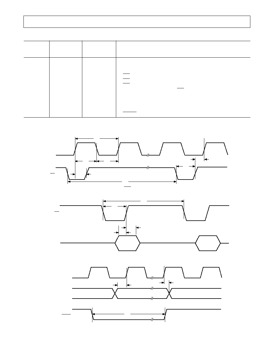
TIMING CHARACTERISTICS
Limit at
T
MIN
to T
MAX
Parameter
(A Version)
Units
Test Conditions/Comments
t
1
20
ns min
MCLK Period
t
2
8
ns min
MCLK High Duration
t
3
8
ns min
MCLK Low Duration
t
4
1
8
ns min
WR
Rising Edge Before MCLK Rising Edge
t
4A
1
8
ns min
WR
Rising Edge After MCLK Rising Edge
t
5
8
ns min
WR
Pulse Width
t
6
t
1
ns min
Duration Between Consecutive WR Pulses
t
7
5
ns min
Data/Address Setup Time
t
8
3
ns min
Data/Address Hold Time
t
9
1
8
ns min
FSELECT, PSEL0, PSEL1 Setup Time Before MCLK Rising Edge
t
9A
1
8
ns min
FSELECT, PSEL0, PSEL1 Setup Time After MCLK Rising Edge
t
10
t
1
ns min
RESET
Pulse Duration
NOTES
1
See Pin Description section.
Guaranteed by design, but not production tested.
t
1
t
2
t
3
t
4A
t
4
t
5
t
6
MCLK
WR
Figure 2. WRMCLK Relationship
A0, A1, A2
DATA
WR
t
6
t
8
t
7
t
5
VALID DATA
VALID DATA
Figure 3. Writing to a Phase/Frequency Register
t
9
VALID DATA
VALID DATA
VALID DATA
t
9A
t
10
MCLK
FSELECT
PSEL0, PSEL1
RESET
Figure 4. Control Timing
(V
DD
= +5 V 5%; AGND = DGND = 0 V, unless otherwise noted)
AD9830
REV. A
4
ABSOLUTE MAXIMUM RATINGS*
(
T
A
= +25
°
C unless otherwise noted)
AVDD to AGND . . . . . . . . . . . . . . . . . . . . . . . 0.3 V to +7 V
DVDD to DGND . . . . . . . . . . . . . . . . . . . . . . 0.3 V to +7 V
AVDD to DVDD . . . . . . . . . . . . . . . . . . . . . . 0.3 V to +0.3 V
AGND to DGND . . . . . . . . . . . . . . . . . . . . . 0.3 V to +0.3 V
Digital I/O Voltage to DGND . . . . . 0.3 V to DVDD + 0.3 V
Analog I/O Voltage to AGND . . . . . 0.3 V to AVDD + 0.3 V
Operating Temperature Range
Industrial (A Version) . . . . . . . . . . . . . . . . 40
°
C to +85
°
C
Storage Temperature Range . . . . . . . . . . . . 65
°
C to +150
°
C
Maximum Junction Temperature . . . . . . . . . . . . . . . . +150
°
C
TQFP
JA
Thermal Impedance . . . . . . . . . . . . . . . . . 75
°
C/W
Lead Temperature, Soldering
Vapor Phase (60 sec) . . . . . . . . . . . . . . . . . . . . . . . +215
°
C
Infrared (15 sec) . . . . . . . . . . . . . . . . . . . . . . . . . . . +220
°
C
*Stresses above those listed under "Absolute Maximum Ratings" may cause
permanent damage to the device. This is a stress rating only and functional
operation of the device at these or any other conditions above those listed in the
operational sections of this specification is not implied. Exposure to abso lute
maximum rating conditions for extended periods may affect device reliability.
WARNING!
ESD SENSITIVE DEVICE
CAUTION
ESD (electrostatic discharge) sensitive device. Electrostatic charges as high as 4000 V readily
accumulate on the human body and test equipment and can discharge without detection.
Although this device features proprietary ESD protection circuitry, permanent damage may
occur on devices subjected to high energy electrostatic discharges. Therefore, proper ESD
precautions are recommended to avoid performance degradation or loss of functionality.
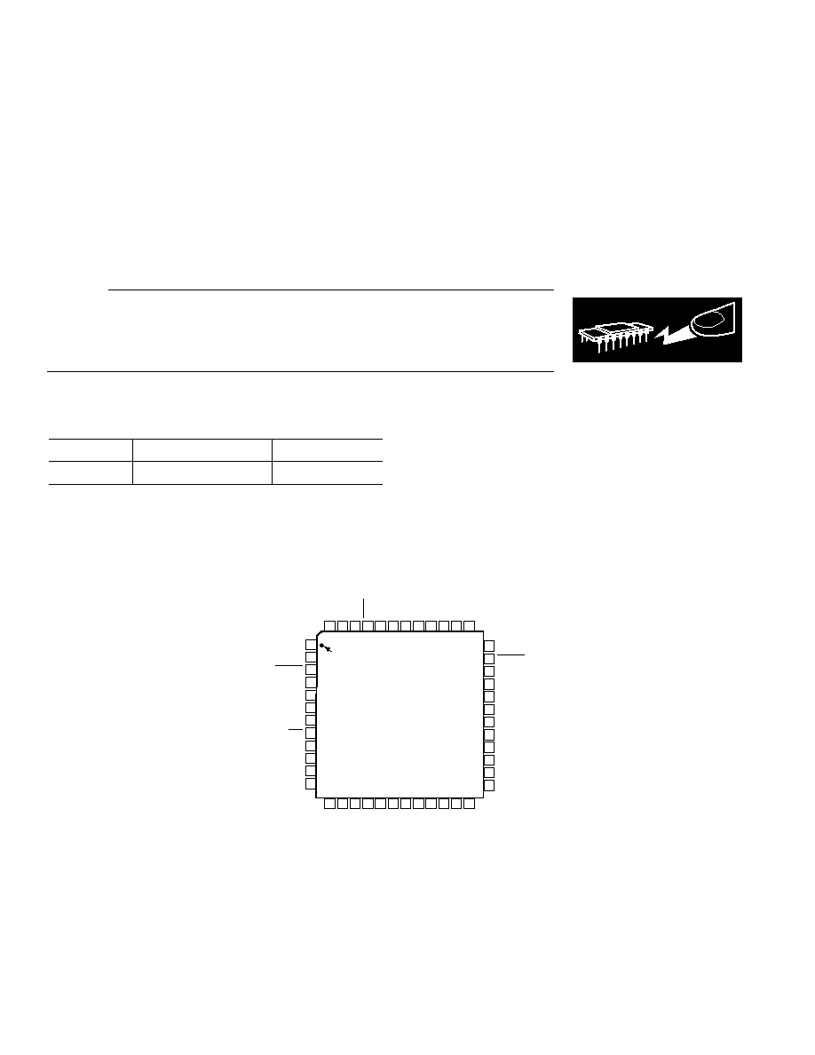
ORDERING GUIDE
Model
Temperature Range
Package Option*
AD9830AST
40
°
C to +85
°
C
ST-48
*ST = Thin Quad Flatpack (TQFP).
PIN CONFIGURATION
36
35
34
33
32
31
30
29
28
27
26
25
NC
AVDD
FS ADJUST
AGND
NC
AGND
AGND
NC
13 14 15 16 17 18 19 20 21 22 23 24
1
2
3
4
5
6
7
8
9
10
11
12
48 47 46 45 44
39 38 37
43 42 41 40
PIN 1
IDENTIFIER
TOP VIEW
(Not to Scale)
AGND
RESET
A0
A1
A2
DB0
DB1
DB11
DGND
DB15
DB14
DB13
DB12
DB10
REFIN
REFOUT
SLEEP
DVDD
DVDD
DGND
MCLK
NC = NO CONNECT
WR
DVDD
FSELECT
PSEL0
DGND
DB2
DB3
DB4
DB9
DB8
DB7
DB6
COMP
AD9830
DB5
PSEL1
DVDD
AVDD
IOUT
IOUT

AD9830
REV. A
5
PIN DESCRIPTION
Mnemonic
Function
POWER SUPPLY
AVDD
Positive power supply for the analog section. A 0.1
µ
F capacitor should be connected between AVDD and
AGND. AVDD has a value of +5 V
±
5%.
AGND
Analog Ground.
DVDD
Positive power supply for the digital section. A 0.1
µ
F decoupling capacitor should be connected between DVDD
and DGND. DVDD has a value of +5 V
±
5%.
DGND
Digital Ground.
ANALOG SIGNAL AND REFERENCE
IOUT, IOUT
Current Output. This is a high impedance current source. A load resistor should be connected between IOUT
and AGND. IOUT should be either tied directly to AGND or through an external load resistor to AGND.
FS ADJUST
Full-Scale Adjust Control. A resistor (R
SET
) is connected between this pin and AGND. This determines the mag-
nitude of the full-scale DAC current. The relationship between R
SET
and the full-scale current is as follows:
IOUT
FULL-SCALE
= 16 V
REFIN
/R
SET
V
REFIN
= 1.21 V nominal, R
SET
= 1 k
typical
REFIN
Voltage Reference Input. The AD9830 can be used with either the on-board reference, which is available from pin
REFOUT, or an external reference. The reference to be used is connected to the REFIN pin. The AD9830 ac-
cepts a reference of 1.21 V nominal.
REFOUT
Voltage Reference Output. The AD9830 has an on-board reference of value 1.21 V nominal. The reference is
made available on the REFOUT pin. This reference is used as the reference to the DAC by connecting REFOUT
to REFIN. REFOUT should be decoupled with a 10 nF capacitor to AGND.
COMP
Compensation pin. This is a compensation pin for the internal reference amplifier. A 10 nF decoupling ceramic
capacitor should be connected between COMP and AVDD.
DIGITAL INTERFACE AND CONTROL
MCLK
Digital Clock Input. DDS output frequencies are expressed as a binary fraction of the frequency of MCLK. The
output frequency accuracy and phase noise are determined by this clock.
FSELECT
Frequency Select Input. FSELECT controls which frequency register, FREQ0 or FREQ1, is used in the phase ac-
cumulator. FSELECT is sampled on the rising MCLK edge. FSELECT needs to be in steady state when an
MCLK rising edge occurs. If FSELECT changes value when an MCLK rising edge occurs, there is an uncertainty
of one MCLK cycle as to when control is transferred to the other frequency register. To avoid any uncertainty, a
change on FSELECT should not coincide with an MCLK rising edge.
WR
Write, Edge-Triggered Digital Input. The WR pin is used when writing data to the AD9830. The data is loaded
into the AD9830 on the rising edge of the WR pulse. This data is then loaded into the destination register on the
MCLK rising edge. The WR pulse rising edge should not coincide with the MCLK rising edge as there will be an
uncertainty of one MCLK cycle regarding the loading of the destination register with the new data. The WR ris-
ing edge should occur before an MCLK rising edge. The data will then be transferred into the destination register
on the MCLK rising edge. Alternatively, the WR rising edge can occur after the MCLK rising edge and the desti-
nation register will be loaded on the next MCLK rising edge.
D0D15
Data Bus, Digital Inputs for destination registers.
A0A2
Address Digital Inputs. These address bits are used to select the destination register to which the digital data is to
be written.
PSEL0, PSEL1
Phase Select Input. The AD9830 has four phase registers. These registers can be used to alter the value being in-
put to the SIN ROM. The contents of the phase register can be added to the phase accumulator output, the inputs
PSEL0 and PSEL1 selecting the phase register to be used. Like the FSELECT input, the AD9830 samples the
PSEL0 and PSEL1 inputs on the MCLK rising edge. Therefore, these inputs should be in steady state at the
MCLK rising edge or, there is an uncertainty of one MCLK cycle as to when control is transferred to the selected
phase register.
SLEEP
Low Power Control, active low digital input. SLEEP puts the AD9830 into a low power mode. Internal clocks
are disabled and the DAC's current sources and REFOUT are turned off. The AD9830 is re-enabled by taking
SLEEP
high.
RESET
Reset, active low digital input. RESET resets the phase accumulator to zero which corresponds to an analog
output of midscale.

AD9830
REV. A
6
TERMINOLOGY
Integral Nonlinearity
This is the maximum deviation of any code from a straight line
passing through the endpoints of the transfer function. The
endpoints of the transfer function are zero scale, a point 0.5
LSB below the first code transition (000 . . . 00 to 000 . . . 01)
and full scale, a point 0.5 LSB above the last code transition
(111 . . . 10 to 111 . . . 11). The error is expressed in LSBs.
Differential Nonlinearity
This is the difference between the measured and the ideal 1 LSB
change between two adjacent codes in the DAC.
Signal to (Noise + Distortion)
Signal to (Noise + Distortion) is measured signal to noise at the
output of the DAC. The signal is the rms magnitude of the fun-
damental. Noise is the rms sum of all the nonfundamental sig-
nals up to half the sampling frequency (f
MCLK
/2) but excluding
the dc component. Signal to (Noise + Distortion) is dependent
on the number of quantization levels used in the digitization
process; the more levels, the smaller the quantization noise.
The theoretical Signal to (Noise + Distortion) ratio for a sine
wave input is given by
Signal to (Noise + Distortion) = (6.02 N + 1.76) dB
where N is the number of bits. Thus, for an ideal 10-bit con-
verter, Signal to (Noise + Distortion) = 61.96 dB.
Total Harmonic Distortion
Total Harmonic Distortion (THD) is the ratio of the rms sum
of harmonics to the rms value of the fundamental. For the
AD9830, THD is defined as
THD
=
20log
(V
2
2
+
V
3
2
+
V
4
2
+
V
5
2
+
V
6
2
V
1
where V
1
is the rms amplitude of the fundamental and V
2
, V
3
,
V
4
, V
5
and V
6
are the rms amplitudes of the second through the
sixth harmonic.
Output Compliance
The output compliance refers to the maximum voltage which
can be generated at the output of the DAC to meet the specifi-
cations. When voltages greater than that specified for the out-
put compliance are generated, the AD9830 may not meet the
specifications listed in the data sheet. For the AD9830, the
maximum voltage which can be generated by the DAC is 1V.
Spurious Free Dynamic Range
Along with the frequency of interest, harmonics of the funda-
mental frequency and images of the MCLK frequency will be
present at the output of a DDS device. The spurious free dy-
namic range (SFDR) refers to the largest spur or harmonic
which is present in the band of interest. The wideband SFDR
gives the magnitude of the largest harmonic or spur relative to
the magnitude of the fundamental frequency in the bandwidth
±
2 MHz about the fundamental frequency. The narrowband
SFDR gives the attenuation of the largest spur or harmonic in a
bandwidth of
±
200 kHz and
±
50 kHz about the fundamental
frequency.
Clock Feedthrough
There will be feedthrough from the MCLK input to the analog
output. The clock feedthrough refers to the magnitude of the
MCLK signal relative to the fundamental frequency in the
AD9830's output spectrum.
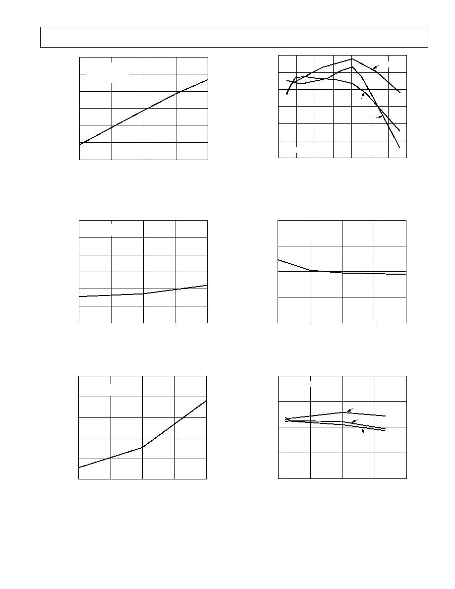
MCLK FREQUENCY MHz
TOTAL CURRENT mA
60
30
10
20
30
40
50
55
50
45
40
35
AVDD = DVDD = +5V
T
A
= +25
°
C
f
OUT
= 200kHz
Figure 5. Typical Current Consumption vs. MCLK
Frequency
MCLK FREQUENCY MHz
SFDR (
±
200kHz) - dB
50
80
10
20
30
40
50
55
60
65
70
75
AVDD = DVDD = +5V
f
OUT
/f
MCLK
= 1/3
Figure 6. Narrow Band SFDR vs. MCLK Frequency
MCLK FREQUENCY MHz
65
10
50
20
SFDR (
±
2MHz
) dB
30
40
50
55
60
40
45
AVDD = DVDD = +5V
f
OUT
/f
MCLK
= 1/3
Figure 7. Wide Band SFDR vs. MCLK Frequency
f
OUT
/f
MCLK
35
65
0
0.35
0.05
0.1
0.15
0.2
0.25
0.3
40
45
50
55
60
AVDD = DVDD = +5V
50MHz
30MHz
10MHz
SFDR (0MCLK/2) dB
Figure 8. WB SFDR vs. f
OUT
/f
MCLK
for Various MCLK
Frequencies
SNR dB
MCLK FREQUENCY MHz
60
55
40
10
50
20
30
40
50
45
AVDD = DVDD = +5V
f
OUT
= f
MCLK
/3
Figure 9. SNR vs. MCLK Frequency
f
OUT
/f
MCLK
60
55
40
0
0.4
0.1
0.2
0.3
50
45
SNR dB
10MHz
30MHz
50MHz
AVDD = DVDD = +5V
Figure 10. SNR vs. f
OUT
/f
MCLK
for Various MCLK
Frequencies
Typical Performance CharacteristicsAD9830
7
REV. A
AD9830
REV. A
8
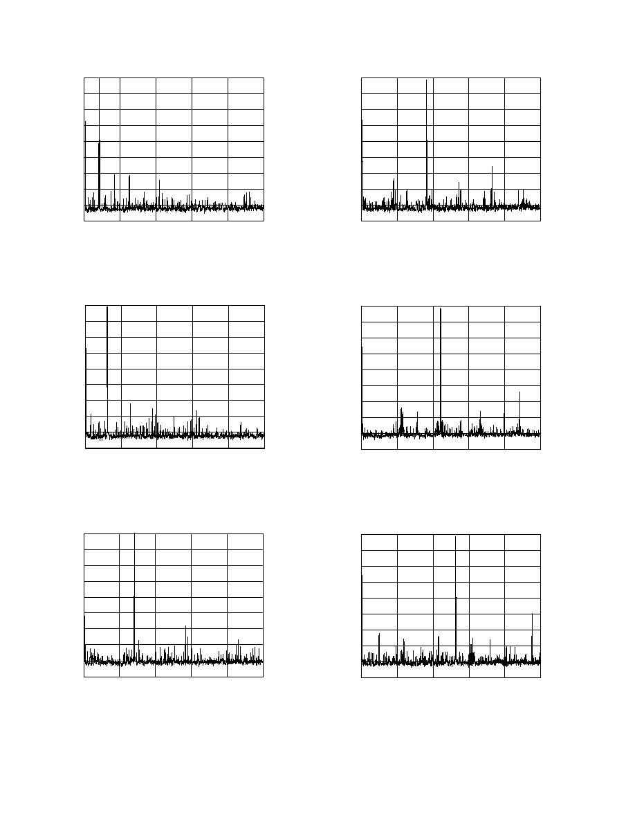
RBW 1kHz VBW 3kHz ST 50 SEC
10dB/DIV
0
10
90
START 0Hz
STOP 25MHz
40
60
70
80
20
30
50
Figure 14. f
MCLK
= 50 MHz, f
OUT
= 9.1 MHz, Frequency
Word = 2E978D50
RBW 1kHz VBW 3kHz ST 50 SEC
10dB/DIV
0
10
90
START 0Hz
STOP 25MHz
40
60
70
80
20
30
50
Figure 15. f
MCLK
= 50 MHz, f
OUT
= 11.1 MHz, Frequency
Word = 38D4FDF4
RBW 1kHz VBW 3kHz ST 50 SEC
10dB/DIV
0
10
90
START 0Hz
STOP 25MHz
40
60
70
80
20
30
50
Figure 16. f
MCLK
= 50 MHz, f
OUT
= 13.1 MHz, Frequency
Word = 43126E98
RBW 1kHz VBW 3kHz ST 50 SEC
10dB/DIV
0
10
90
START 0Hz
STOP 25MHz
40
60
70
80
20
30
50
Figure 11.
f
MCLK
= 50 MHz, f
OUT
= 2.1 MHz, Frequency
Word = ACO8312
RBW 1kHz VBW 3kHz ST 50 SEC
10dB/DIV
0
10
90
START 0Hz
STOP 25MHz
40
60
70
80
20
30
50
Figure 12. f
MCLK
= 50 MHz, f
OUT
= 3.1 MHz, Frequency
Word = FDF3B64
RBW 1kHz VBW 3kHz ST 50 SEC
10dB/DIV
0
10
90
START 0Hz
STOP 25MHz
40
60
70
80
20
30
50
Figure 13. f
MCLK
= 50 MHz, f
OUT
= 7.1 MHz, Frequency
Word = 245A1CAC
AD9830
REV. A
9
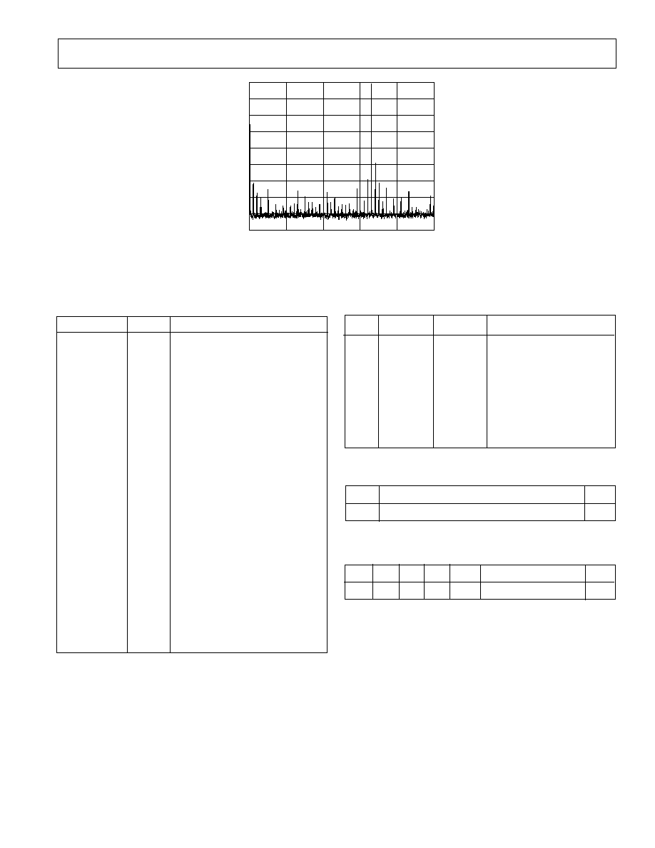
RBW 1kHz VBW 3kHz ST 50 SEC
10dB/DIV
0
10
90
START 0Hz
STOP 25MHz
40
60
70
80
20
30
50
Figure 17. f
MCLK
= 50 MHz, f
OUT
= 16.5 MHz, Frequency
Word = 547AE148
Register
Size
Description
FREQ0 REG
32 Bits
Frequency Register 0. This defines
the output frequency, when
FSELECT = 0, as a fraction of the
MCLK frequency.
FREQ1 REG
32 Bits
Frequency Register 1. This de-
fines the output frequency, when
FSELECT = 1, as a fraction of the
MCLK frequency.
PHASE0 REG
12 Bits
Phase Offset Register 0. When
PSEL0 = PSEL1 = 0, the contents
of this register are added to the out-
put of the phase accumulator.
PHASE1 REG
12 Bits
Phase Offset Register 1. When
PSEL0 = 1 and PSEL1 = 0, the
contents of this register are added
to the output of the phase
accumulator.
PHASE2 REG
12 Bits
Phase Offset Register 2. When
PSEL0 = 0 and PSEL1 = 1, the
contents of this register are added
to the output of the phase
accumulator.
PHASE3 REG
12 Bits
Phase Offset Register 3. When
PSEL0 = PSEL1 = 1, the contents
of this register are added to the out-
put of the phase accumulator.
Figure 18. AD9830 Control Registers
A2
A1
A0
Destination Register
0
0
0
FREQ0 REG 16 LSBs
0
0
1
FREQ0 REG 16 MSBs
0
1
0
FREQ1 REG 16 LSBs
0
1
1
FREQ1 REG 16 MSBs
1
0
0
PHASE0 REG
1
0
1
PHASE1 REG
1
1
0
PHASE2 REG
1
1
1
PHASE3 REG
Figure 19. Addressing the Control Registers
D15
D0
MSB
LSB
Figure 20. Frequency Register Bits
D15
D14 D13 D12 D11
D0
X
X
X
X
MSB
LSB
X = Don't Care
Figure 21. Phase Register Bits
AD9830
REV. A
10
CIRCUIT DESCRIPTION
The AD9830 provides an exciting new level of integration
for the RF/Communications system designer. The AD9830
combines the Numerical Controlled Oscillator (NCO), SINE
Look-Up table, Frequency and Phase Modulators, and a
Digital-to-Analog Converter on a single integrated circuit.
The internal circuitry of the AD9830 consists of three main
sections. These are:
Numerical Controlled Oscillator (NCO) + Phase Modulator
SINE Look-Up Table
Digital-to-Analog Converter
The AD9830 is a fully integrated Direct Digital Synthesis
(DDS) chip. The chip requires one reference clock, two low
precision resistors and eight decoupling capacitors to provide
digitally created sine waves up to 25 MHz. In addition to the
generation of this RF signal, the chip is fully capable of a broad
range of simple and complex modulation schemes. These
modulation schemes are fully implemented in the digital do-
main allowing accurate and simple realization of complex
modulation algorithms using DSP techniques.
THEORY OF OPERATION
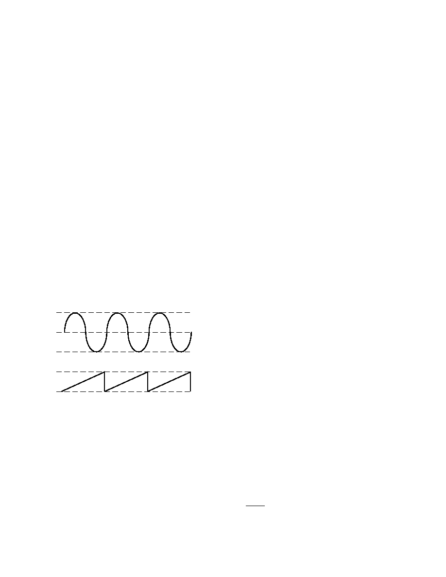
Sine waves are typically thought of in terms of their magnitude
form a (t) = sin (
t). However, these are nonlinear and not
easy to generate except through piece wise construction. On
the other hand, the angular information is linear in nature.
That is, the phase angle rotates through a fixed angle for each
unit of time. The angular rate depends on the frequency of the
signal by the traditional rate of
= 2
f
MAGNITUDE
PHASE
+1
0
1
2
0
Figure 22. Sine Wave
Knowing that the phase of a sine wave is linear and given a ref-
erence interval (clock period), the phase rotation for that period
can be determined.
Phase =
t
Solving for
=
Phase/
t = 2
f
Solving for f and substituting the reference clock frequency for
the reference period (1/f
MCLK
=
t)
f =
Phase
×
f
MCLK
/2
The AD9830 builds the output based on this simple equation.
A simple DDS chip can implement this equation with three
major subcircuits.
Numerical Controlled Oscillator + Phase Modulator
This consists of two frequency select registers, a phase accumu-
lator and four phase offset registers. The main component of
the NCO is a 32-bit phase accumulator which assembles the
phase component of the output signal. Continuous time signals
have a phase range of 0 to 2
. Outside this range of numbers,
the sinusoid functions repeat themselves in a periodic manner.
The digital implementation is no different. The accumulator
simply scales the range of phase numbers into a multibit digital
word. The phase accumulator in the AD9830 is implemented
with 32 bits. Therefore, in the AD9830, 2
= 2
32
. Likewise,
the
Phase term is scaled into this range of numbers 0 <
Phase
< 2
32
1. Making these substitutions into the equation above
f =
Phase
×
f
MCLK
/2
32
where 0 <
Phase < 2
32
With a clock signal of 50 MHz and a phase word of 051EB852
hex
f = 51EB852
×
50 MHz/2
32
= 1.000000000931 MHz
The input to the phase accumulator (i.e., the phase step) can be
selected either from the FREQ0 Register or FREQ1 Register
and this is controlled by the FSELECT pin. NCOs inherently
generate continuous phase signals, thus avoiding any output
discontinuity when switching between frequencies. More com-
plex frequency modulation schemes can be implemented by up-
dating the contents of these registers. This facilitates complex
frequency modulation schemes, such as GMSK.
Following the NCO, a phase offset can be added to perform
phase modulation using the 12-bit PHASE Registers. The con-
tents of this register are added to the most significant bits of the
NCO. The AD9830 has four PHASE registers. The resolution
of the phase registers equals 2
/4096.
Sine Look-Up Table (LUT)
To make the output useful, the signal must be converted from
phase information into a sinusoidal value. Since phase informa-
tion maps directly into amplitude, a ROM LUT converts the
phase information into amplitude. To do this, the digital phase
information is used to address a sine ROM LUT. Although the
NCO contains a 32-bit phase accumulator, the output of the
NCO is truncated to 12 bits. Using the full resolution of the
phase accumulator is impractical and unnecessary as this would
require a look-up table of 2
32
entries.
It is necessary only to have sufficient phase resolution in the
LUTs such that the dc error of the output waveform is domi-
nated by the quantization error in the DAC. This requires the
look-up table to have two more bits of phase resolution than the
10-bit DAC.
Digital-to-Analog Converter
The AD9830 includes a high impedance current source 10-bit
DAC, capable of driving a wide range of loads at different
speeds. Full-scale output current can be adjusted, for optimum
power and external load requirements, through the use of a
single external resistor (R
SET
).
The DAC can be configured for single or differential ended op-
eration. IOUT can be tied directly to AGND for single ended
operation or through a load resistor to develop an output volt-
age. The load resistor can be any value required, as long as the
AD9830
REV. A
11
full-scale voltage developed across it does not exceed the voltage
compliance range. Since full-scale current is controlled by R
SET
,
adjustments to R
SET
can balance changes made to the load resistor.
However, if the DAC full-scale output current is significantly less
than 20 mA, the linearity of the DAC may degrade.
DSP and MPU Interfacing
The AD9830 has a parallel interface, with 16 bits of data being
loaded during each write cycle.
The frequency or phase registers are loaded by asserting the WR
signal. The destination register for the 16-bit data is selected
using the address inputs A0, A1 and A2. The phase registers
are 12 bits wide so, only the 12 LSBs need to be valid--the
4 MSBs of the 16 bit word do not have to contain valid data.
Data is loaded into the AD9830 by pulsing WR low, the data
being latched into the AD9830 on the rising edge of WR. The
values of inputs A0, A1 and A2 are also latched into the
AD9830 on the WR rising edge. The appropriate register is up-
dated on the next MCLK rising edge. To ensure that the
AD9830 contains valid data at the rising edge of MCLK, the
rising edge of the WR pulse should not coincide with the rising
MCLK edge. The WR pulse must occur several nanoseconds
before the MCLK rising edge. If the WR rising edge occurs at
the MCLK rising edge, there is an uncertainty of one MCLK
cycle regarding the loading of the destination register--the desti-
nation register may be loaded with the new data immediately or
the destination register may be updated on the next MCLK ris-
ing edge. To avoid any uncertainty, the times listed in the speci-
fications should be complied with.
FSELECT, PSEL0 and PSEL1 are sampled on the MCLK
rising edge. Again, these inputs should be valid when an
MCLK rising edge occurs as there will be an uncertainty of one
MCLK cycle introduced otherwise. When these inputs change
value, there will be a pipeline delay before control is transferred
to the selected register--there will be a pipeline delay before the
analog output is controlled by the selected register. Similarly,
there is a delay when a new word is written to a register. PSEL0,
PSEL1, FSELECT and WR have latencies of six MCLK cycles.
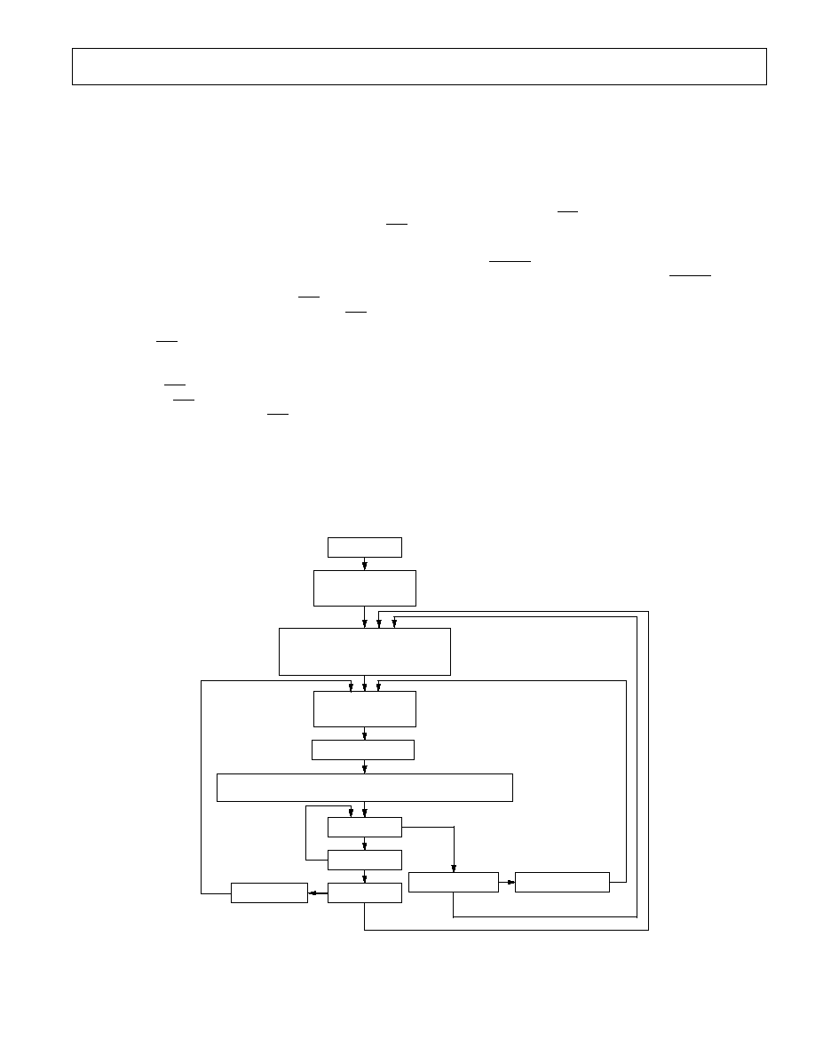
The flow chart in Figure 23 shows the operating routine for the
AD9830. When the AD9830 is powered up, the part should be
reset using RESET. This will reset the phase accumulator to
zero so that the analog output is at midscale. RESET does not
reset the phase and frequency registers. These registers will con-
tain invalid data and, therefore, should be set to zero by the user.
The registers to be used should be loaded, the analog output be-
ing f
MCLK
/2
32
×
FREG where FREG is the value contained in
the selected frequency register. This signal will be phase shifted
by an amount 2
/4096
×
PHASEREG where PHASEREG is the
value contained in the selected phase register. When FSELECT,
PSEL0 and PSEL1 are programmed, there will be a pipeline de-
lay of approximately 6 MCLK cycles before the analog output
reacts to the change on these inputs.
RESET
DATA WRITE
FREG<0, 1> = 0
PHASEREG<0, 1, 2, 3> = 0
DATA WRITE
FREG<0> = f
OUT
0/f
MCLK
*2
32
FREG<1> = f
OUT
1/f
MCLK
*2
32
PHASEREG<3:0> = DELTA PHASE<0, 1, 2, 3>
SELECT DATA SOURCES
SET FSELECT
SET PSEL0, PSEL1
DAC OUTPUT
V
OUT
= V
REFIN
*8*R
OUT
/R
SET*
(1 + SIN(2
(FREG*f
MCLK
*t/2
32
+ PHASEREG/2
12
)))
WAIT 6 MCLK CYCLES
CHANGE PHASE?
CHANGE FOUT?
CHANGE FREG?
YES
CHANGE PHASEREG?
CHANGE PSEL0, PSEL1
YES
NO
NO
CHANGE FSELECT
YES
NO
YES
NO
Figure 23. Flow Chart for AD9830 Initialization and Operation
AD9830
REV. A
12
APPLICATIONS
The AD9830 contains functions which make it suitable for
modulation applications. The part can be used to perform
simple modulation such as FSK. More complex modulation
schemes such as GMSK and QPSK can also be implemented
using the AD9830. In a FSK application, the two frequency reg-
isters of the AD9830 are loaded with different values, one fre-
quency will represent the space frequency while the other will
represent the mark frequency. The digital data stream is fed to
the FSELECT pin which will cause the AD9830 to modulate
the carrier frequency between the two values.
The AD9830 has four phase registers which enable the part to
perform PSK. With phase shift keying, the carrier frequency is
phase shifted, the phase being altered by an amount which is
related to the bit stream being input to the modulator. The
presence of four shift registers eases the interaction needed
between the DSP and the AD9830.
The frequency and phase registers can be written to continuously,
if required. The maximum update rate equals the frequency of
the MCLK. However, if a selected register is loaded with a new
word, there will be a delay of 6 MCLK cycles before the analog
output will change accordingly.
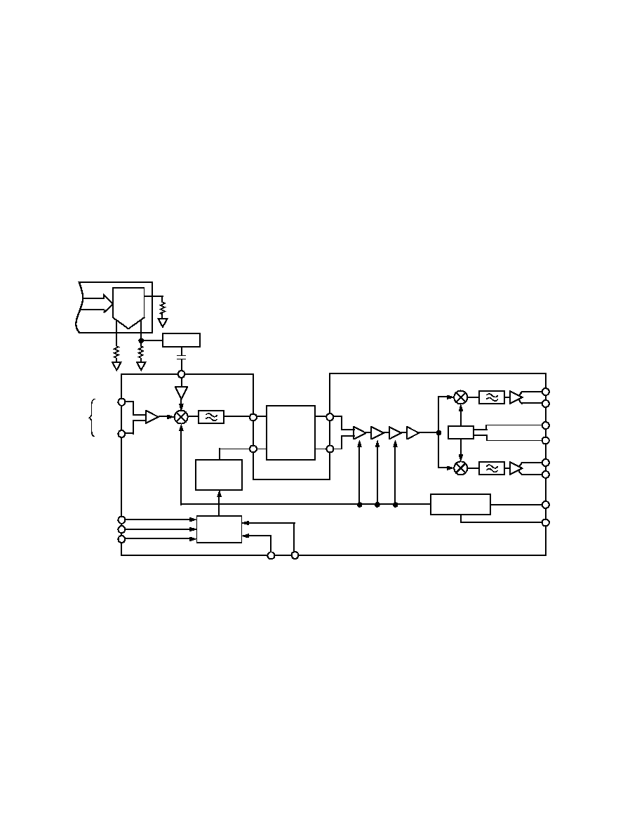
The AD9830 is also suitable for signal generator applications.
With its low current consumption, the part is suitable for
mobile applications in which it can be used as a local oscillator.
Figure 24 shows the interface between the AD9830 and AD6459
which is a down converter used on the receive side of mobile
phones or basestations.
BANDPASS
FILTER
IFIP
IFIM
MXOP
MXOM
MIDPOINT
BIAS
GENERATOR
BIAS
CIRCUIT
LOIP
FILTER
51
51
10 BITS
R
SET
1k
AD9830
AD6459
PLL
0
°
90
°
GAIN TC
COMPENSATION
IRxP
IRxN
FREF
FLTR
QRxP
QRxN
GAIN
GREF
RFHI
RFLO
VPS1
VPS2
PRUP
COM1
COM2
0.1µF
ANTENNA
Figure 24. AD9830 and AD6459 Receiver Circuit
AD9830
REV. A
13
Grounding and Layout
The printed circuit board that houses the AD9830 should be
designed so that the analog and digital sections are separated
and confined to certain areas of the board. This facilitates the
use of ground planes which can be separated easily. A mini-
mum etch technique is generally best for ground planes as it
gives the best shielding. Digital and analog ground planes
should only be joined in one place. If the AD9830 is the only
device requiring an AGND to DGND connection, then the
ground planes should be connected at the AGND and DGND
pins of the AD9830. If the AD9830 is in a system where mul-
tiple devices require AGND to DGND connections, the con-
nection should be made at one point only, a star ground point
that should be established as close as possible to the AD9830.
Avoid running digital lines under the device as these will couple
noise onto the die. The analog ground plane should be allowed
to run under the AD9830 to avoid noise coupling. The power
supply lines to the AD9830 should use as large a track as is pos-
sible to provide low impedance paths and reduce the effects of
glitches on the power supply line. Fast switching signals like
clocks should be shielded with digital ground to avoid radiating
noise to other sections of the board. Avoid crossover of digital
and analog signals. Traces on opposite sides of the board
should run at right angles to each other. This will reduce the ef-
fects of feedthrough through the board. A microstrip technique
is by far the best but is not always possible with a double-sided
board. In this technique, the component side of the board is
dedicated to ground planes while signals are placed on the other
side.
Good decoupling is important. The analog and digital supplies
to the AD9830 are independent and separately pinned out to
minimize coupling between analog and digital sections of the
device. All analog and digital supplies should be decoupled to
AGND and DGND respectively with 0.1
µ
F ceramic capacitors
in parallel with 10
µ
F tantalum capacitors. To achieve the best
from the decoupling capacitors, they should be placed as close
as possible to the device, ideally right up against the device. In
systems where a common supply is used to drive both the AVDD
and DVDD of the AD9830, it is recommended that the system's
AVDD supply be used. This supply should have the recom-
mended analog supply decoupling between the AVDD pins of
the AD9830 and AGND and the recommended digital supply
decoupling capacitors between the DVDD pins and DGND.
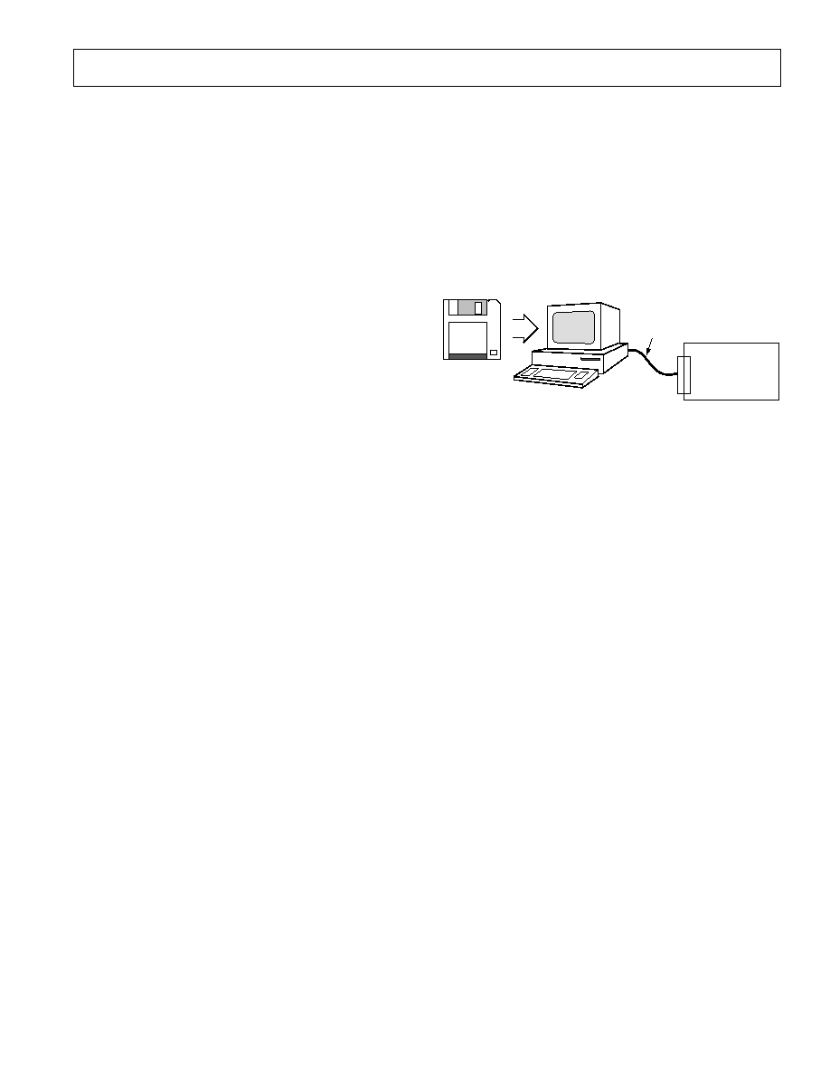
AD9830 Evaluation Board
The AD9830 Evaluation Board allows designers to evaluate the
high performance AD9830 DDS Modulator with a minimum of
effort.
To prove that this device will meet the user's waveform synthesis
requirements, the user only requires a +5 V power supply, an
IBM-compatible PC and a spectrum analyzer along with the
evaluation board. The evaluation setup is shown below.
The DDS Evaluation kit includes a populated, tested AD9830
printed circuit board along with software which controls the
AD9830 in a Windows environment.
AD9830.EXE
IBM COMPATIBLE PC
PARALLEL PORT
CENTRONICS
PRINTER CABLE
AD9830 EVALUATION
BOARD
Figure 25. AD9830 Evaluation Board Setup
Using the AD9830 Evaluation Board
The AD9830 Evaluation kit is a test system designed to simplify
the evaluation of the AD9830. Provisions to control the AD9830
from the printer port of an IBM-compatible PC are included
along with the necessary software. An application note is also
available with the evaluation board which gives information on
operating the evaluation board.
Prototyping Area
An area is available on the evaluation board where the user can
add additional circuits to the evaluation test set. Users may
want to build custom analog filters for the outputs or add buf-
fers and operational amplifiers which are to be used in the final
application.
XO vs. External Clock
The AD9830 can operate with master clocks up to 50 MHz. A
50 MHz oscillator is included on the evaluation board. How-
ever, this oscillator can be removed and an external CMOS
clock connected to the part, if required.
Power Supply
Power to the AD9830 evaluation board must be provided exter-
nally through the pin connections. The power leads should be
twisted to reduce ground loops.
AD9830
REV. A
14
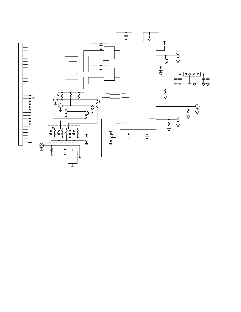
COMPONENT LIST
Integrated Circuits
U1
AD9830 (48-Pin TQFP)
U2, U3
74HC574 Latches
XTAL1
OSC XTAL 50 MHz
Capacitors
C9, C11
10
µ
F Tantalum Capacitor
C8, C10, C12C14
0.1
µ
F Ceramic Capacitor
C1C5
0.1
µ
F Ceramic Chip Capacitor
C6, C7
10 nF Ceramic Capacitor
Resistors
R5
1 k
Resistor
R6, R7
51
Resistor
R4
50
Resistor
R1R3
10 k
Resistor
Links
LK5
Two Pin Link
LK1, LK2, LK3, LK4
Three Pin Link
Switch
SW
End Stackable Switch (SDC
Double Throw)
Sockets
SMB1SMB7
Sub-Miniature BNC Connector
Connectors
J2, J3
PCB Mounting Terminal Block
J1
36-Pin Edge Connector
1
2
3
4
5
6
7
8
9
10
11
12
13
14
15
16
17
18
19
20
21
22
23
24
25
26
27
28
29
30
31
32
33
34
35
36
LATCH
D0
D1
D2
D3
D4
D5
D6
D7
LOAD
WR
RESET
WR
RESET
LATCH
LOAD
D7
D0
J1
PC INTERFACE
V
DD
CK
74HC574
0.1µF
C13
DVDD
LOAD
U2
V
DD
CK
74HC574
0.1µF
C14
DVDD
LATCH
U3
14
21
22
31
32
34
D15
D8
D7
D0
A2
A0
WR
RESET
8
35
WR
RESET
12
11
10
7
3
PSEL1
PSEL0
FSELECT
MCLK
SLEEP
LK1
LK2
LK3
R3
10k
R1
10k
R2
10k
SMB1
SMB2
SMB3
AVDD
DVDD
10µF
C9
0.1µF
C8
0.1µF
C10
10µF
C11
J2
DVDD
SW
DVDD
DGND
OUT
U4
DVDD
C12
0.1µF
R4
50
SMB4
MCLK
DVDD
LK4
DGND
AGND
6,13, 29
36, 39, 41, 46
COMP
REFIN
REFOUT
FSADJUST
IOUT
IOUT
DVDD
4, 5, 9, 25
AVDD
38, 43
0.1µF
C1, C2, C3
0.1µF
C4, C5
AD9830
U1
AVDD
48
10nF
C6
10nF
C7
1
2
LK5
SMB5
1k
R5
SMB7
51
R7
47
44
45
SMB6
51
R6
DVDD
AVDD
XTAL1
J3
Figure 26. Evaluation Board Layout
AD9830
REV. A
15
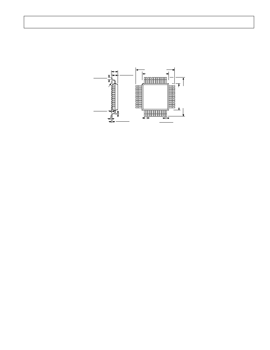
OUTLINE DIMENSIONS
Dimensions shown in inches and (mm).
48-Lead TQFP
(ST-48)
0.354 (9.00) BSC
0.276 (7.0) BSC
1
12
13
25
24
36
37
48
TOP VIEW
(PINS DOWN)
0.276 (7.0) BSC
0.354 (9.00) BSC
0.011 (0.27)
0.006 (0.17)
0.019 (0.5)
BSC
SEATING
PLANE
0.063 (1.60) MAX
0
°
MIN
0
°
7
°
0.006 (0.15)
0.002 (0.05)
0.030 (0.75)
0.018 (0.45)
0.057 (1.45)
0.053 (1.35)
0.030 (0.75)
0.018 (0.45)
0.007 (0.18)
0.004 (0.09)

PRINTED IN U.S.A.
16
C2142a109/96