 | ÐлекÑÑоннÑй компоненÑ: AD9822 | СкаÑаÑÑ:  PDF PDF  ZIP ZIP |
Äîêóìåíòàöèÿ è îïèñàíèÿ www.docs.chipfind.ru
REV. A
Information furnished by Analog Devices is believed to be accurate and
reliable. However, no responsibility is assumed by Analog Devices for its
use, nor for any infringements of patents or other rights of third parties
which may result from its use. No license is granted by implication or
otherwise under any patent or patent rights of Analog Devices.
a
AD9822
One Technology Way, P.O. Box 9106, Norwood, MA 02062-9106, U.S.A.
Tel: 781/329-4700
World Wide Web Site: http://www.analog.com
Fax: 781/326-8703
© Analog Devices, Inc., 1999
Complete 14-Bit
CCD/CIS Signal Processor
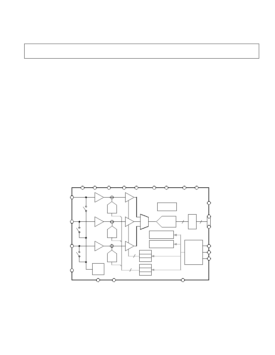
FUNCTIONAL BLOCK DIAGRAM
9-BIT
DAC
PGA
CDS
PGA
CDS
PGA
CDS
3:1
MUX
14-BIT
ADC
14
14:8
MUX
8
BANDGAP
REFERENCE
CONFIGURATION
REGISTER
MUX
REGISTER
BLUE
GREEN
RED
BLUE
GREEN
RED
6
9
GAIN
REGISTERS
OFFSET
REGISTERS
DIGITAL
CONTROL
INTERFACE
INPUT
CLAMP
BIAS
AD9822
DRVDD
DRVSS
AVDD
AVSS
CAPT
CAPB
AVDD
AVSS
CML
OEB
DOUT
SCLK
SLOAD
SDATA
ADCCLK
CDSCLK2
CDSCLK1
OFFSET
VINB
VING
VINR
9-BIT
DAC
9-BIT
DAC
FEATURES
14-Bit 15 MSPS A/D Converter
No Missing Codes Guaranteed
3-Channel Operation Up to 15 MSPS
1-Channel Operation Up to 12.5 MSPS
Correlated Double Sampling
16x Programmable Gain
350 mV Programmable Offset
Input Clamp Circuitry
Internal Voltage Reference
Multiplexed Byte-Wide Output (8+6 Format)
3-Wire Serial Digital Interface
3 V/5 V Digital I/O Compatibility
28-Lead SOIC or SSOP
Low Power CMOS: 385 mW (Typ)
Power-Down Mode: <1 mW
APPLICATIONS
Flatbed Document Scanners
Film Scanners
Digital Color Copiers
Multifunction Peripherals
PRODUCT DESCRIPTION
The AD9822 is a complete analog signal processor for CCD
imaging applications. It features a 3-channel architecture
designed to sample and condition the outputs of trilinear
color CCD arrays. Each channel consists of an input clamp,
Correlated Double Sampler (CDS), offset DAC and Pro-
grammable Gain Amplifier (PGA), multiplexed to a high
performance 14-bit A/D converter.
The CDS amplifiers may be disabled for use with sensors such
as Contact Image Sensors (CIS) and CMOS active pixel sensors,
which do not require CDS.
The 14-bit digital output is multiplexed into an 8-bit output
word that is accessed using two read cycles. The internal
registers are programmed through a 3-wire serial interface, and
provide adjustment of the gain, offset, and operating mode.
The AD9822 operates from a single 5 V power supply, typically
consumes 385 mW of power, and is packaged in a 28-lead SOIC
or SSOP.
REV. A
2
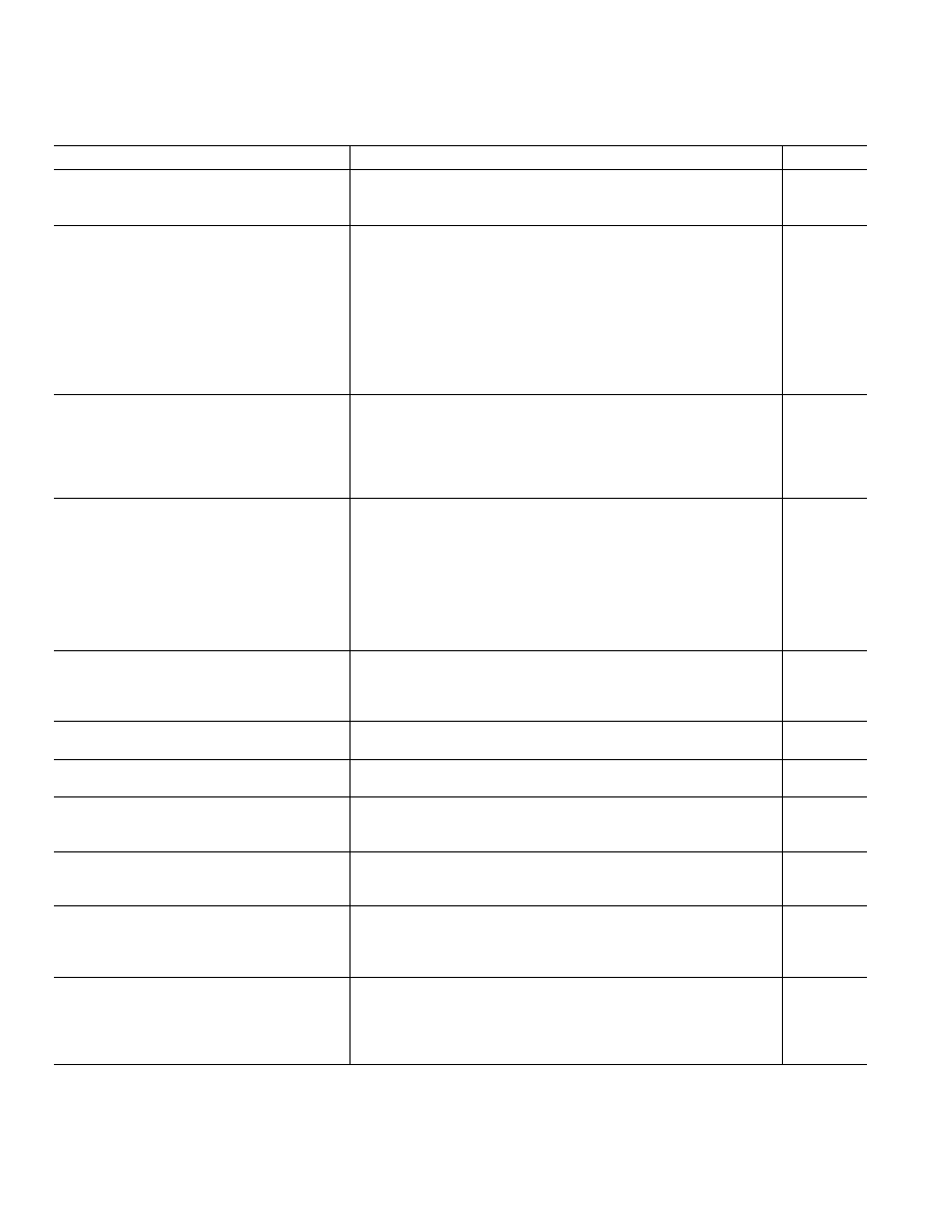
AD9822SPECIFICATIONS
ANALOG SPECIFICATIONS
Parameter
Min
Typ
Max
Unit
MAXIMUM CONVERSION RATE
3-Channel Mode with CDS
15
MSPS
1-Channel Mode with CDS
12.5
MSPS
ACCURACY (Entire Signal Path)
ADC Resolution
14
Bits
Integral Nonlinearity
(INL)
17.0/+3.5
LSB
INL @ 6 MHz
10.5/+1.5
LSB
Differential Nonlinearity (DNL)
0.65/+0.75
LSB
DNL @ 6 MHz
1.0
0.6/+0.65
+1.1
LSB
No Missing Codes
14
Bits
No Missing Codes @ 6 MHz
14
Bits
Offset Error
240
19
+200
mV
Gain Error
1.4
+3.5
+6.9
% FSR
ANALOG INPUTS
Input Signal Range
1
2.0
V p-p
Allowable Reset Transient
1
1.0
V
Input Limits
2
AVSS 0.3
AVDD + 0.3
V
Input Capacitance
10
pF
Input Bias Current
10
nA
AMPLIFIERS
PGA Gain at Minimum
1
V/V
PGA Gain at Maximum
5.7
V/V
PGA Gain Resolution
2
64
Steps
PGA Gain Monotonicity
Guaranteed
Programmable Offset at Minimum
350
mV
Programmable Offset at Maximum
+350
mV
Programmable Offset Resolution
512
Steps
Programmable Offset Monotonicity
Guaranteed
NOISE AND CROSSTALK
Total Output Noise @ PGA Minimum
1.5
LSB rms
Total Output Noise @ PGA Maximum
6.0
LSB rms
Channel-Channel Crosstalk @ 6 MHz
<1
LSB
POWER SUPPLY REJECTION
AVDD = +5 V
±
0.25 V
0.063
0.9
% FSR
DIFFERENTIAL VREF (@ 25
°
C)
CAPTCAPB (2 V ADC Full-Scale Range)
0.94
1.0
1.06
V
TEMPERATURE RANGE
Operating
0
+70
°
C
Storage
65
+150
°
C
POWER SUPPLIES
AVDD
4.75
5.0
5.25
V
DRVDD
3.0
5.0
5.25
V
OPERATING CURRENT
AVDD
73
mA
DRVDD
4
mA
Power-Down Mode Current
150
µ
A
POWER DISSIPATION
3-Channel Mode
385
450
mW
3-Channel Mode @ 6 MHz
335
410
mW
1-Channel Mode
300
mW
1-Channel Mode @ 6 MHz
250
mW
(T
MIN
to T
MAX
, AVDD = 5 V, DRVDD = 5 V, CDS Mode, f
ADCCLK
= 15 MHz, f
CDSCLK1
= f
CDSCLK2
= 5 MHz, PGA
Gain = 1, unless otherwise noted.)
3
REV. A
DIGITAL SPECIFICATIONS
Parameter
Symbol
Min
Typ
Max
Unit
LOGIC INPUTS
High Level Input Voltage
V
IH
2.0
V
Low Level Input Voltage
V
IL
0.8
V
High Level Input Current
I
IH
10
µ
A
Low Level Input Current
I
IL
10
µ
A
Input Capacitance
C
IN
10
pF
LOGIC OUTPUTS
High Level Output Voltage
V
OH
4.5
V
Low Level Output Voltage
V
OL
0.1
V
High Level Output Current
I
OH
50
µ
A
Low Level Output Current
I
OL
50
µ
A
Specifications subject to change without notice.
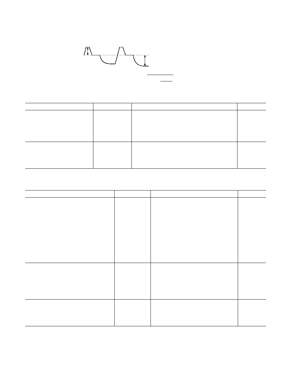
TIMING SPECIFICATIONS
Parameter
Symbol
Min
Typ
Max
Unit
CLOCK PARAMETERS
3-Channel Pixel Rate
t
PRA
67
ns
1-Channel Pixel Rate
t
PRB
80
ns
ADCCLK Pulsewidth
t
ADCLK
30
ns
CDSCLK1 Pulsewidth
t
C1
10
ns
CDSCLK2 Pulsewidth
t
C2
10
ns
CDSCLK1 Falling to CDSCLK2 Rising
t
C1C2
0
ns
ADCCLK Falling to CDSCLK2 Rising
t
ADC2
0
ns
CDSCLK2 Rising to ADCCLK Rising
t
C2ADR
0
ns
CDSCLK2 Falling to ADCCLK Falling
t
C2ADF
30
40
ns
CDSCLK2 Falling to CDSCLK1 Rising
t
C2C1
30
40
ns
ADCCLK Falling to CDSCLK1 Rising
t
ADC1
0
ns
Aperture Delay for CDS Clocks
t
AD
2
ns
SERIAL INTERFACE
Maximum SCLK Frequency
f
SCLK
10
MHz
SLOAD to SCLK Setup Time
t
LS
10
ns
SCLK to SLOAD Hold Time
t
LH
10
ns
SDATA to SCLK Rising Setup Time
t
DS
10
ns
SCLK Rising to SDATA Hold Time
t
DH
10
ns
SCLK Falling to SDATA Valid
t
RDV
10
ns
DATA OUTPUT
Output Delay
t
OD
8
ns
3-State to Data Valid
t
DV
10
ns
Output Enable High to 3-State
t
HZ
10
ns
Latency (Pipeline Delay)
3 (Fixed)
Cycles
Specifications subject to change without notice.
(T
MIN
to T
MAX
, AVDD = 5 V, DRVDD = 5 V, CDS Mode, f
ADCCLK
= 15 MHz, f
CDSCLK1
= f
CDSCLK2
= 5 MHz,
C
L
= 10 pF, unless otherwise noted.)
(T
MIN
to T
MAX
, AVDD = 5 V, DRVDD = 5 V)
NOTES
1
Linear input signal range is from 2 V to 4 V when the CCD's reference level is clamped to 4 V by the AD9822's input clamp.
1V TYP
RESET TRANSIENT
4V SET BY INPUT CLAMP (3V OPTION ALSO AVAILABLE)
2V p-p MAX INPUT SIGNAL RANGE
2
The PGA Gain is approximately "linear in dB" and follows the equation:
Gain
=
+
[
.
. [
]
]
5 7
1
4 7
63 G
63
where G is the register value. See Figure 13.
Specifications subject to change without notice.
AD9822
REV. A
AD9822
4
CAUTION
ESD (electrostatic discharge) sensitive device. Electrostatic charges as high as 4000 V readily
accumulate on the human body and test equipment and can discharge without detection.
Although the AD9822 features proprietary ESD protection circuitry, permanent damage may
occur on devices subjected to high energy electrostatic discharges. Therefore, proper ESD
precautions are recommended to avoid performance degradation or loss of functionality.
WARNING!
ESD SENSITIVE DEVICE
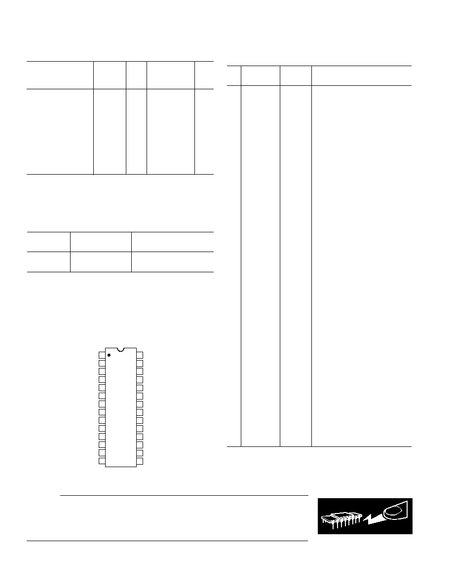
ABSOLUTE MAXIMUM RATINGS
*
With
Respect
Parameter
To
Min
Max
Unit
VIN, CAPT, CAPB
AVSS
0.3
AVDD + 0.3
V
Digital Inputs
AVSS
0.3
AVDD + 0.3
V
AVDD
AVSS
0.5
+6.5
V
DRVDD
DRVSS
0.5
+6.5
V
AVSS
DRVSS
0.3
+0.3
V
Digital Outputs
DRVSS
0.3
DRVDD + 0.3
V
Junction Temperature
150
°
C
Storage Temperature
65
+150
°
C
Lead Temperature
(10 sec)
300
°
C
*Stresses above those listed under Absolute Maximum Ratings may cause perma-
nent damage to the device. This is a stress rating only; functional operation of the
device at these or other conditions above those indicated in the operational
sections of this specification is not implied. Exposure to absolute maximum ratings
for extended periods may affect device reliability.
ORDERING GUIDE
Temperature
Package
Model
Range
Description
AD9822JR
0
°
C to 70
°
C
28-Lead 300 Mil SOIC
AD9822JRS
0
°
C to 70
°
C
28-Lead 5.3 mm SSOP
THERMAL CHARACTERISTICS
Thermal Resistance
28-Lead 300 Mil SOIC
28-Lead 5.3 mm SSOP
JA
= 71.4
°
C/W
JA
= 109
°
C/W
JC
= 23
°
C/W
JC
= 39
°
C/W
PIN CONFIGURATION
TOP VIEW
(Not to Scale)
28
27
26
25
24
23
22
21
20
19
18
17
16
15
1
2
3
4
5
6
7
8
9
10
11
12
13
14
AD9822
CDSCLK1
AVDD
CDSCLK2
AVSS
ADCCLK
VINR
OEB
OFFSET
DRVDD
VING
DRVSS
CML
(MSB) D7
VINB
D6
CAPT
D5
CAPB
D4
AVSS
D3
AVDD
D2
SLOAD
D1
SCLK
(LSB) D0
SDATA
PIN FUNCTION DESCRIPTIONS
Pin
N
o.
Name
Type
Description
1
CDSCLK1
DI
CDS Reference Level Sampling
Clock
2
CDSCLK2
DI
CDS Data Level Sampling Clock
3
ADCCLK
DI
A/D Converter Sampling Clock
4
OEB
DI
Output Enable, Active Low
5
DRVDD
P
Digital Output Driver Supply
6
DRVSS
P
Digital Output Driver Ground
7
D7
DO
Data Output MSB. ADC DB13
High Byte, ADC DB5 Low Byte
8
D6
DO
Data Output. ADC DB12 High
Byte, ADC DB4 Low Byte
9
D5
DO
Data Output. ADC DB11 High
Byte, ADC DB3 Low Byte
10
D4
DO
Data Output. ADC DB10 High
Byte, ADC DB2 Low Byte
11
D3
DO
Data Output. ADC DB9 High
Byte, ADC DB1 Low Byte
12
D2
DO
Data Output. ADC DB8 High
Byte, ADC DB0 Low Byte
13
D1
DO
Data Output. ADC DB7 High
Byte, Don't Care Low Byte
14
D0
DO
Data Output LSB. ADC DB6
High Byte, Don't Care Low Byte
15
SDATA
DI/DO
Serial Interface Data Input/Output
16
SCLK
DI
Serial Interface Clock Input
17
SLOAD
DI
Serial Interface Load Pulse
18
AVDD
P
5 V Analog Supply
19
AVSS
P
Analog Ground
20
CAPB
AO
ADC Bottom Reference Voltage
Decoupling
21
CAPT
AO
ADC Top Reference Voltage
Decoupling
22
VINB
AI
Analog Input, Blue Channel
23
CML
AO
Internal Bias Level Decoupling
24
VING
AI
Analog Input, Green Channel
25
OFFSET
AO
Clamp Bias Level Decoupling
26
VINR
AI
Analog Input, Red Channel
27
AVSS
P
Analog Ground
28
AVDD
P
5 V Analog Supply
TYPE: AI = Analog Input, AO = Analog Output, DI = Digital Input, DO =
Digital Output, P = Power.

REV. A
AD9822
5
DEFINITIONS OF SPECIFICATIONS
INTEGRAL NONLINEARITY (INL)
Integral nonlinearity error refers to the deviation of each individual
code from a line drawn from "zero scale" through "positive full
scale." The point used as "zero scale" occurs 1/2 LSB before
the first code transition. "Positive full scale" is defined as a level
1 1/2 LSB beyond the last code transition. The deviation is
measured from the middle of each particular code to the true
straight line.
DIFFERENTIAL NONLINEARITY (DNL)
An ideal ADC exhibits code transitions that are exactly 1 LSB
apart. DNL is the deviation from this ideal value. Thus every
code must have a finite width. No missing codes guaranteed to
14-bit resolution indicates that all 16384 codes, respectively,
must be present over all operating ranges.
OFFSET ERROR
The first ADC code transition should occur at a level 1/2 LSB
above the nominal zero scale voltage. The offset error is the
deviation of the actual first code transition level from the
ideal level.
GAIN ERROR
The last code transition should occur for an analog value
1 1/2 LSB below the nominal full-scale voltage. Gain error is
the deviation of the actual difference between first and last code
transitions and the ideal difference between the first and last
code transitions.
INPUT REFERRED NOISE
The rms output noise is measured using histogram techniques.
The ADC output codes' standard deviation is calculated in LSB,
and converted to an equivalent voltage, using the relationship
1 LSB = 4 V/16384 = 244 mV. The noise is then referred to the
input of the AD9822 by dividing by the PGA gain.
CHANNEL-TO-CHANNEL CROSSTALK
In an ideal 3-channel system, the signal in one channel will not
influence the signal level of another channel. The channel-to-
channel crosstalk specification is a measure of the change that
occurs in one channel as the other two channels are varied. In the
AD9822, one channel is grounded and the other two channels
are exercised with full-scale input signals. The change in the
output codes from the first channel is measured and compared
with the result when all three channels are grounded. The
difference is the channel-to-channel crosstalk, stated in LSB.
APERTURE DELAY
The aperture delay is the time delay that occurs from when a
sampling edge is applied to the AD9822 until the actual sample
of the input signal is held. Both CDSCLK1 and CDSCLK2
sample the input signal during the transition from high to low,
so the aperture delay is measured from each clock's falling edge
to the instant the actual internal sample is taken.
POWER SUPPLY REJECTION
Power Supply Rejection specifies the maximum full-scale change
that occurs from the initial value when the supplies are varied
over the specified limits.
REV. A
AD9822
6
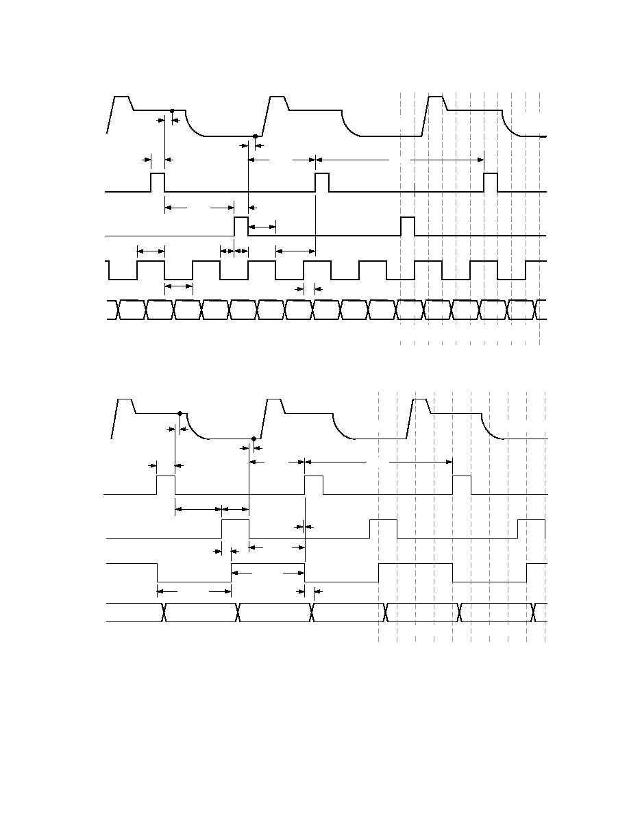
PIXEL N (R, G, B)
PIXEL (N+1)
t
AD
t
C2
t
C2ADF
t
ADC2
t
C2ADR
t
ADCLK
t
ADCLK
t
OD
ANALOG
INPUTS
CDSCLK2
ADCCLK
OUTPUT
DATA
D<7:0>
R (N2)
G (N2)
G (N2)
B (N2)
B (N2)
R (N1)
R (N1)
G (N1)
G (N1)
B (N1)
B (N1)
R (N)
R (N)
G (N)
G (N)
HIGH
BYTE
LOW
BYTE
HIGH
BYTE
LOW
BYTE
HIGH
BYTE
LOW
BYTE
HIGH
BYTE
LOW
BYTE
HIGH
BYTE
LOW
BYTE
HIGH
BYTE
LOW
BYTE
HIGH
BYTE
LOW
BYTE
t
ADC1
t
C2C1
t
PRA
t
AD
t
C1
t
C1C2
CDSCLK1
PIXEL
(N+2)
Figure 1. 3-Channel CDS Mode Timing
t
AD
PIXEL N
t
AD
ANALOG
INPUTS
t
OD
CDSCLK2
ADCCLK
OUTPUT
DATA
D<7:0>
t
C2
t
C2ADF
t
ADCLK
t
ADCLK
PIXEL (N4)
PIXEL (N4)
PIXEL (N3)
PIXEL (N3)
PIXEL (N2)
PIXEL (N2)
t
C1C2
t
C1
CDSCLK1
t
ADC1
t
C2C1
HIGH BYTE
LOW BYTE
LOW BYTE
HIGH BYTE
LOW BYTE
HIGH BYTE
PIXEL (N+1)
t
PRB
PIXEL (N+2)
t
C2ADR
Figure 2. 1-Channel CDS Mode Timing
REV. A
AD9822
7
PIXEL N (R, G, B)
PIXEL (N+1)
t
AD
t
PRA
t
C2
t
C2ADF
t
ADC2
t
C2ADR
t
ADCLK
t
ADCLK
t
OD
ANALOG
INPUTS
CDSCLK2
ADCCLK
OUTPUT
DATA
D<7:0>
R (N2)
G (N2)
G (N2)
B (N2)
B (N2)
R (N1)
R (N1)
G (N1)
G (N1)
B (N1)
B (N1)
R (N)
R (N)
G (N)
G (N)
HIGH
BYTE
LOW
BYTE
HIGH
BYTE
LOW
BYTE
HIGH
BYTE
LOW
BYTE
HIGH
BYTE
LOW
BYTE
HIGH
BYTE
LOW
BYTE
HIGH
BYTE
LOW
BYTE
HIGH
BYTE
LOW
BYTE
Figure 3. 3-Channel SHA Mode Timing
t
PRB
t
OD
ANALOG
INPUTS
CDSCLK2
ADCCLK
OUTPUT
DATA
D<7:0>
t
C2
PIXEL N
t
AD
t
C2ADF
t
ADCLK
t
ADCLK
HIGH BYTE
LOW BYTE
LOW BYTE
HIGH BYTE
HIGH BYTE
LOW BYTE
PIXEL (N4)
PIXEL (N4)
PIXEL (N3)
PIXEL (N3)
PIXEL (N2)
PIXEL (N2)
t
C2ADR
Figure 4. 1-Channel SHA Mode Timing
REV. A
AD9822
8
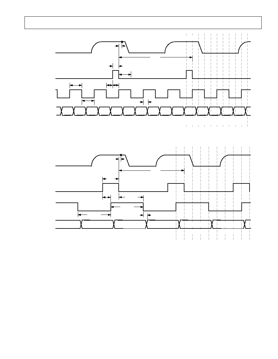
t
HZ
t
DV
t
OD
t
OD
ADCCLK
OUTPUT
DATA
<D7:D0>
OEB
HIGH BYTE
DB13DB6
LOW BYTE
DB5DB0
HIGH BYTE
N+1
LOW
BYTE
N+1
LOW
BYTE
N+2
HIGH
BYTE
N+3
PIXEL N
PIXEL N
Figure 5. Digital Output Data Timing
SDATA
SCLK
SLOAD
R/Wb
A2
A1
A0
XX
XX
D8
D7
D6
D5
D4
D3
D2
D1
D0
t
DS
t
DH
t
LS
t
LH
XX
Figure 6. Serial Write Operation Timing
SDATA
SCLK
SLOAD
R/Wb
A2
A1
A0
XX
XX
XX
D8
D7
D6
D5
D4
D3
D2
D1
D0
t
DS
t
RDV
t
DH
t
LS
t
LH
Figure 7. Serial Read Operation Timing

REV. A
AD9822
9
FUNCTIONAL DESCRIPTION
The AD9822 can be operated in four different modes: 3-Channel
CDS Mode, 3-Channel SHA Mode, 1-Channel CDS Mode,
and 1-Channel SHA Mode. Each mode is selected by program-
ming the Configuration Register through the serial interface.
For more detail on CDS or SHA mode operation, see the
Circuit Operation section.
3-Channel CDS Mode
In 3-Channel CDS Mode, the AD9822 simultaneously samples
the red, green and blue input voltages from the CCD outputs.
The sampling points for each Correlated Double Sampler (CDS)
are controlled by CDSCLK1 and CDSCLK2 (see Figures 8 and
9). CDSCLK1's falling edge samples the reference level of the
CCD waveform. CDSCLK2's falling edge samples the data
level of the CCD waveform. Each CDS amplifier outputs the
difference between the CCD's reference and data levels. Next,
the output voltage of each CDS amplifier is level-shifted by an
Offset DAC. The voltages are then scaled by the three Program-
mable Gain Amplifiers before being multiplexed through the
14-bit ADC. The ADC sequentially samples the PGA outputs
on the falling edges of ADCCLK.
The offset and gain values for the red, green and blue channels
are programmed using the serial interface. The order in which
the channels are switched through the multiplexer is selected by
programming the MUX register.
Timing for this mode is shown in Figure 1. It is recommended
that the falling edge of CDSCLK2 occur coincident with or before
the rising edge of ADCCLK, although this is not required
to satisfy the minimum timing constraints. The rising edge of
CDSCLK2 should not occur before the previous falling edge of
ADCCLK, as shown by t
ADC2
. The output data latency is three
clock cycles.
3-Channel SHA Mode
In 3-Channel SHA Mode, the AD9822 simultaneously samples
the red, green and blue input voltages. The sampling point is
controlled by CDSCLK2. CDSCLK2's falling edge samples the
input waveforms on each channel. The output voltages from the
three SHAs are modified by the offset DACs and then scaled by
the three PGAs. The outputs of the PGAs are then multiplexed
through the 14-bit ADC. The ADC sequentially samples the
PGA outputs on the falling edges of ADCCLK.
The input signal is sampled with respect to the voltage applied
to the OFFSET pin (see Figure 10). With the OFFSET pin
grounded, a zero volt input corresponds to the ADC's zero-scale
output. The OFFSET pin may also be used as a coarse offset
adjust pin. A voltage applied to this pin will be subtracted from
the voltages applied to the red, green, and blue inputs in the
first amplifier stage of the AD9822. The input clamp is dis-
abled in this mode. For more information, see the Circuit
Operation section.
Timing for this mode is shown in Figure 2. CDSCLK1 should
be grounded in this mode. Although not required, it is recom-
mended that the falling edge of CDSCLK2 occur coincident
with or before the rising edge of ADCCLK. The rising edge of
CDSCLK2 should not occur before the previous falling edge of
ADCCLK, as shown by t
ADC2
. The output data latency is three
ADCCLK cycles.
The offset and gain values for the red, green, and blue channels
are programmed using the serial interface. The order in which
the channels are switched through the multiplexer is selected by
programming the MUX register.
1-Channel CDS Mode
This mode operates in the same way as the 3-Channel CDS
mode. The difference is that the multiplexer remains fixed in
this mode, so only the channel specified in the MUX register is
processed.
Timing for this mode is shown in Figure 3.
1-Channel SHA Mode
This mode operates in the same way as the 3-Channel SHA
mode, except that the multiplexer remains stationary. Only the
channel specified in the MUX register is processed.
The input signal is sampled with respect to the voltage applied
to the OFFSET pin. With the OFFSET pin grounded, a zero
volt input corresponds to the ADC's zero scale output. The
OFFSET pin may also be used as a coarse offset adjust pin. A
voltage applied to this pin will be subtracted from the voltages
applied to the red, green, and blue inputs in the first amplifier
stage of the AD9822. The input clamp is disabled in this mode.
For more information, see the Circuit Operation section.
Timing for this mode is shown in Figure 4. CDSCLK1 should
be grounded in this mode of operation.
REV. A
AD9822
10
INTERNAL REGISTER DESCRIPTIONS
Table I. Internal Register Map
Register
Address
Data Bits
Name
A2
A1
A0
D8
D7
D6
D5
D4
D3
D2
D1
D0
Configuration
0
0
0
0
0
VREF
3Ch/1Ch
CDS On
Clamp
Pwr Dn
0
0
MUX
0
0
1
0
RGB/BGR
Red
Green
Blue
0
0
0
0
Red PGA
0
1
0
0
0
0
MSB
LSB
Green PGA
0
1
1
0
0
0
MSB
LSB
Blue PGA
1
0
0
0
0
0
MSB
LSB
Red Offset
1
0
1
MSB
LSB
Green Offset
1
1
0
MSB
LSB
Blue Offset
1
1
1
MSB
LSB
Configuration Register
The Configuration Register controls the AD9822's operating mode and bias levels. Bits D8, D1, and D0 should always be set low.
Bit D7 sets the full-scale voltage range of the AD9822's A/D converter to either 4 V (high) or 2 V (low). Bit D6 controls the internal
voltage reference. If the AD9822's internal voltage reference is used, this bit is set high. Setting Bit D6 low will disable the internal
voltage reference, allowing an external voltage reference to be used. Bit D5 will configure the AD9822 for either the 3-Channel (high)
or 1-Channel (low) mode of operation. Setting Bit D4 high will enable the CDS mode of operation, and setting this bit low will
enable the SHA mode of operation. Bit D3 sets the dc bias level of the AD9822's input clamp. This bit should always be set high for
the 4 V clamp bias, unless a CCD with a reset feedthrough transient exceeding 2 V is used. If the 3 V clamp bias level is used, the
peak-to-peak input signal range to the AD9822 is reduced to 3 V maximum. Bit D2 controls the power-down mode. Setting Bit D2
high will place the AD9822 into a very low power "sleep" mode. All register contents are retained while the AD9822 is in the powered-
down state.
Table II. Configuration Register Settings
D8
D7
D6
D5
D4
D3
D2
D1
D0
Set
Set
Internal VREF
# of Channels
CDS Operation
Input Clamp Bias
Power-Down
Set
Set
to
to
1 = Enabled
*
1 = 3-Ch Mode
*
1 = CDS Mode
*
1 = 4 V
*
1 = On
to
to
0
0
0 = Disabled
0 = 1-Ch Mode
0 = SHA Mode
0 = 3 V
0 = Off (Normal)
* 0
0
*Power-on default value.
MUX Register
The MUX Register controls the sampling channel order in the AD9822. Bits D8, D3, D2, D1, and D0 should always be set low. Bit
D7 is used when operating in 3-Channel Mode. Setting Bit D7 high will sequence the MUX to sample the red channel first, then the
green channel, and then the blue channel. When in this mode, the CDSCLK2 pulse always resets the MUX to sample the red channel
first (see Timing Figure 1). When Bit D7 is set low, the channel order is reversed to blue first, green second, and red third. The
CDSCLK2 pulse will always reset the MUX to sample the blue channel first. Bits D6, D5, and D4 are used when operating in
1-Channel Mode. Bit D6 is set high to sample the red channel. Bit D5 is set high to sample the green channel. Bit D4 is set high to
sample the blue channel. The MUX will remain stationary during 1-Channel Mode.
Table III. MUX Register Settings
D8
D7
D6
D5
D4
D3
D2
D1
D0
Set
3-Channel Select
1-Channel Select
1-Channel Select
1-Channel Select
Set
Set
Set
Set
to
1 = R-G-B
*
1 = RED
*
1 = GREEN
1 = BLUE
to
to
to
to
0
0 = B-G-R
0 = Off
0 = Off
*
0 = Off
*
0
0
0
0
*Power-on default value.
REV. A
AD9822
11
PGA Gain Registers
There are three PGA registers for individually programming the gain in the red, green, and blue channels. Bits D8, D7, and D6 in
each register must be set low, and bits D5 through D0 control the gain range in 64 increments. See Figure 13 for a graph of the PGA
Gain versus PGA register code. The coding for the PGA registers is straight binary, with an all "zeros" word corresponding to the
minimum gain setting (1x) and an all "ones" word corresponding to the maximum gain setting (5.7x).
Table IV. PGA Gain Register Settings
D8
D7
D6
D5
D4
D3
D2
D1
D0
Gain (V/V)
Gain (dB)
Set to 0
Set to 0
Set to 0
MSB
LSB
0
0
0
0
0
0
0
0
0
*
1.0
0.0
0
0
0
0
0
0
0
0
1
1.013
0.12
·
·
·
·
·
·
·
·
·
0
0
0
1
1
1
1
1
0
5.4
14.6
0
0
0
1
1
1
1
1
1
5.7
15.1
*Power-on default value.
Offset Registers
There are three PGA registers for individually programming the offset in the red, green, and blue channels. Bits D8 through D0
control the offset range from 350 mV to +350 mV in 512 increments. The coding for the offset registers is sign magnitude, with D8
as the sign bit. Table V shows the offset range as a function of the Bits D8 through D0.
Table V. Offset Register Settings
D8
D7
D6
D5
D4
D3
D2
D1
D0
Offset (mV)
MSB
LSB
0
0
0
0
0
0
0
0
0
*
0
0
0
0
0
0
0
0
0
1
+1.2
·
·
·
·
·
·
0
1
1
1
1
1
1
1
1
+350
1
0
0
0
0
0
0
0
0
0
1
0
0
0
0
0
0
0
1
1.2
·
·
·
·
·
·
1
1
1
1
1
1
1
1
1
350
*Power-on default value.
REV. A
AD9822
12
CIRCUIT OPERATION
Analog Inputs--CDS Mode
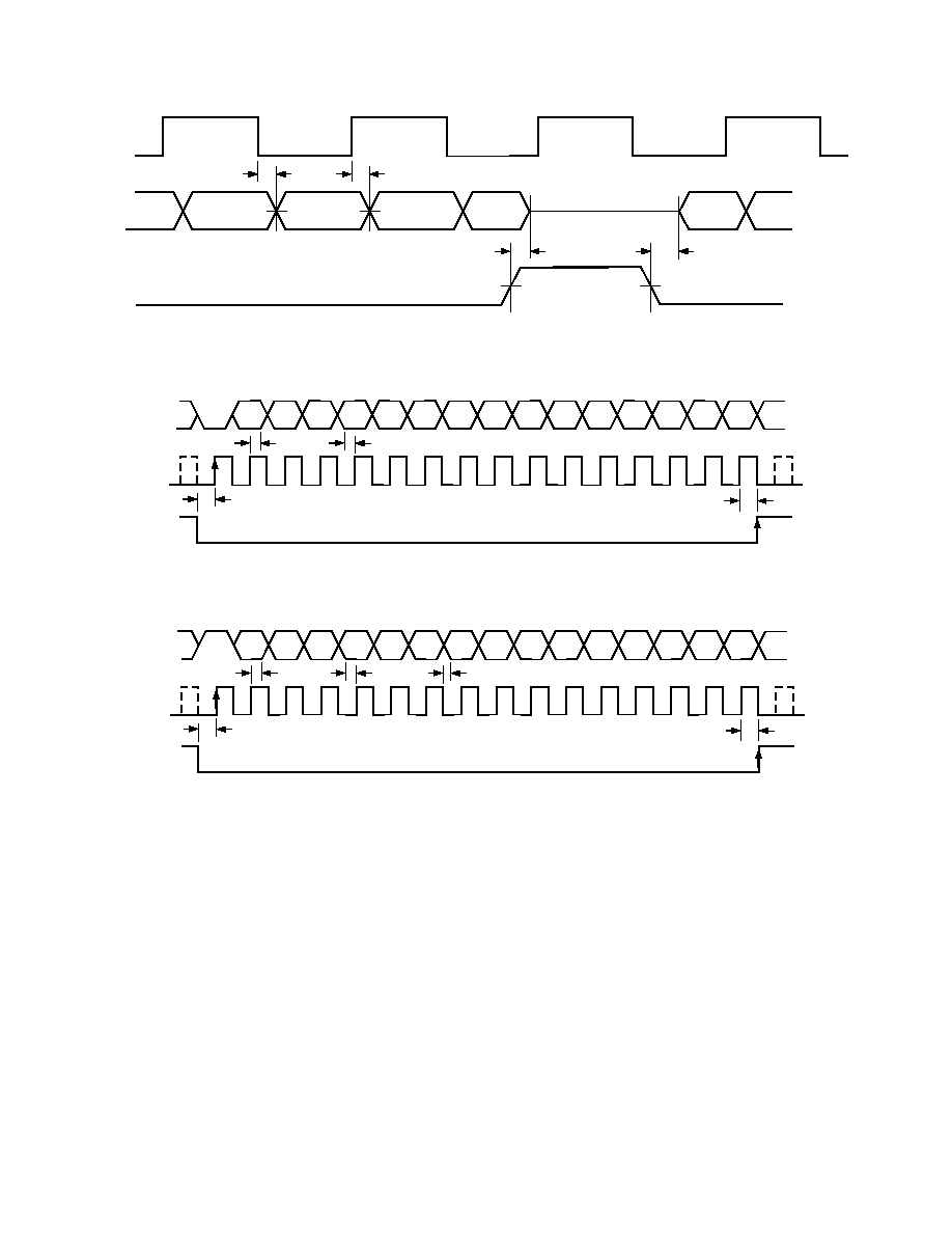
Figure 8 shows the analog input configuration for the CDS
mode of operation. Figure 9 shows the internal timing for the
sampling switches. The CCD reference level is sampled when
CDSCLK1 transitions from high to low, opening S1. The CCD
data level is sampled when CDSCLK2 transitions from high to
low, opening S2. S3 is then closed, generating a differential output
voltage representing the difference between the two sampled levels.
The input clamp is controlled by CDSCLK1. When CDSCLK1
is high, S4 closes and the internal bias voltage is connected to
the analog input. The bias voltage charges the external 0.1
µ
F
input capacitor, level-shifting the CCD signal into the AD9822's
input common-mode range. The time constant of the input
clamp is determined by the internal 5 k
resistance and the
external 0.1
µ
F input capacitance.
AD9822
S1
S2
2pF
S3
2pF
CML
CML
AVDD
4V
S4
5k
1.7k
VINR
OFFSET
C
IN
0.1 F
CCD SIGNAL
0.1 F
1 F
+
3V
2.2k
6.9k
INPUT CLAMP LEVEL
IS SELECTED IN THE
CONFIGURATION
REGISTER
Figure 8. CDS-Mode Input Configuration (All Three Chan-
nels Are Identical)
CDSCLK1
CDSCLK2
Q3
(INTERNAL)
S1, S4 CLOSED
S1, S4 CLOSED
S2 CLOSED
S2 CLOSED
S3 CLOSED
S3 CLOSED
S3 OPEN
S2 OPEN
S1, S4 OPEN
Figure 9. CDS-Mode Internal Switch Timing
External Input Coupling Capacitors
The recommended value for the input coupling capacitors is
0.1
µ
F. While it is possible to use a smaller capacitor, this larger
value is chosen for several reasons:
1. Signal Attenuation. The input coupling capacitor creates a
capacitive divider with a CMOS integrated circuit's input
capacitance, attenuating the CCD signal level. C
IN
should be
large relative to the IC's 10 pF input capacitance in order to
minimize this effect.
2. Linearity. Some of the input capacitance of a CMOS IC is
junction capacitance, which varies nonlinearly with applied
voltage. If the input coupling capacitor is too small, then the
attenuation of the CCD signal will vary nonlinearly with signal
level. This will degrade the system linearity performance.
3. Sampling Errors. The internal 2 pF sample capacitors have
a "memory" of the previously sampled pixel. There is a
charge redistribution error between C
IN
and the internal
sample capacitors
for larger pixel-to-pixel voltage swings. As
the value of C
IN
is reduced, the resulting error in the sampled
voltage will increase. With a C
IN
value of 0.1
µ
F, the charge
redistribution error will be less than 1 LSB for a full-scale
pixel-to-pixel voltage swing.
Analog Inputs--SHA Mode
Figure 10 shows the analog input configuration for the SHA
mode of operation. Figure 11 shows the internal timing for the
sampling switches. The input signal is sampled when CDSCLK2
transitions from high to low, opening S1. The voltage on the
OFFSET pin is also sampled on the falling edge of CDSCLK2,
when S2 opens. S3 is then closed, generating a differential out-
put voltage representing the difference between the sampled
input voltage and the OFFSET voltage. The input clamp is
disabled during SHA mode operation.
AD9822
S1
2pF
S3
CML
VINR
INPUT SIGNAL
S2
2pF
CML
OFFSET
RED
VING
GREEN
VINB
BLUE
OPTIONAL DC OFFSET
(OR CONNECT TO GND)
Figure 10. SHA-Mode Input Configuration (All Three
Channels Are Identical)
CDSCLK2
Q3
(INTERNAL)
S1, S2 CLOSED
S1, S2 CLOSED
S3 CLOSED
S3 CLOSED
S3 OPEN
S1, S2 OPEN
Figure 11. SHA-Mode Internal Switch Timing
REV. A
13
AD9822
Figure 12 shows how the OFFSET pin may be used in a CIS
application for coarse offset adjustment. Many CIS signals have
dc offsets ranging from several hundred millivolts to more than
1 V. By connecting the appropriate dc voltage to the OFFSET
pin, the CIS signal will be restored to "zero." After the large dc
offset is removed, the signal can be scaled using the PGA to
maximize the ADC's dynamic range.
AD9822
OFFSET
RED-OFFSET
GREEN-OFFSET
BLUE-OFFSET
VINR
VING
VINB
RED
GREEN
BLUE
0.1 F
AVDD
VREF FROM
CIS MODULE
DC OFFSET
R1
R2
SHA
SHA
SHA
Figure 12. SHA-Mode Used with External DC Offset
Programmable Gain Amplifiers
The AD9822 uses one Programmable Gain Amplifier (PGA) for
each channel. Each PGA has a gain range from 1x (0 dB) to
5.8x (15.5 dB), adjustable in 64 steps. Figure 6 shows the PGA
gain as a function of the PGA register code. Although the gain
curve is approximately "linear in dB", the gain in V/V varies
nonlinearly with register code, following the equation:
Gain
G
=
+
-
5 7
1
4 7
63
63
.
.
where G is the decimal value of the gain register contents, and
varies from 0 to 63.
PGA REGISTER VALUE Decimal
15
0
GAIN dB ( )
12
9
6
3
0
4
8
12 16 20 24 28 32 36 40 44 48 52 56 60 63
5.7
5.0
4.0
3.0
2.0
1.0
GAIN V/V ( )
Figure 13. PGA Gain Transfer Function
REV. A
AD9822
14
28
27
26
25
24
23
22
21
20
19
18
17
16
15
1
2
3
4
5
6
7
8
9
10
11
12
13
14
AD9822
CDSCLK1
AVDD
CDSCLK2
ADCCLK
OEB
DRVDD
DRVSS
D7 (MSB)
D6
D5
D4
D3
D2
D1
D0 (LSB)
AVSS
VINR
OFFSET
VING
CML
VINB
CAPT
CAPB
AVSS
AVDD
SLOAD
SCLK
SDATA
3
CLOCK INPUTS
8
DATA OUTPUTS
0.1 F
3
SERIAL INTERFACE
0.1 F
5V/3V
5V
0.1 F
0.1 F
0.1 F
0.1 F
RED INPUT
GREEN INPUT
BLUE INPUT
0.1 F
0.1 F
1.0 F
10 F
0.1 F
+
0.1 F
5V
0.1 F
Figure 14. Recommended Circuit Configuration, 3-Channel CDS Mode
28
27
26
25
24
23
22
21
20
19
18
17
16
15
1
2
3
4
5
6
7
8
9
10
11
12
13
14
AD9822
CDSCLK1
AVDD
CDSCLK2
ADCCLK
OEB
DRVDD
DRVSS
D7 (MSB)
D6
D5
D4
D3
D2
D1
D0 (LSB)
AVSS
VINR
OFFSET
VING
CML
VINB
CAPT
CAPB
AVSS
AVDD
SLOAD
SCLK
SDATA
3
CLOCK INPUTS
8
DATA OUTPUTS
0.1 F
3
SERIAL INTERFACE
0.1 F
5V/3V
5V
0.1 F
RED INPUT
GREEN INPUT
BLUE INPUT
0.1 F
10 F
0.1 F
+
0.1 F
5V
0.1 F
Figure 15. Recommended Circuit Configuration, 3-Channel SHA Mode
(Analog Inputs Sampled with Respect to Ground)
APPLICATIONS INFORMATION
Circuit and Layout Recommendations
The recommended circuit configuration for 3-Channel CDS
mode operation is shown in Figure 14. The recommended input
coupling capacitor value is 0.1
µ
F (see Circuit Operation section
for more details). A single ground plane is recommended for the
AD9822. A separate power supply may be used for DRVDD,
the digital driver supply, but this supply pin should still be
decoupled to the same ground plane as the rest of the AD9822.
The loading of the digital outputs should be minimized, either
by using short traces to the digital ASIC, or by using external
digital buffers. To minimize the effect of digital transients during
major output code transitions, the falling edge of CDSCLK2
should occur coincident with or before the rising edge of
ADCCLK (see Figures 1 through 4 for timing). All 0.1
µ
F
decoupling capacitors should be located as close as possible to
the AD9822 pins. When operating in single channel mode, the
unused analog inputs should be grounded.
Figure 15 shows the recommended circuit configuration for 3-
Channel SHA mode. All of the above considerations also apply
for this configuration, except that the analog input signals are
directly connected to the AD9822 without the use of coupling
capacitors. The analog input signals must already be dc-biased
between 0 V and 2 V (see the Circuit Operation section for
more details).
REV. A
AD9822
15
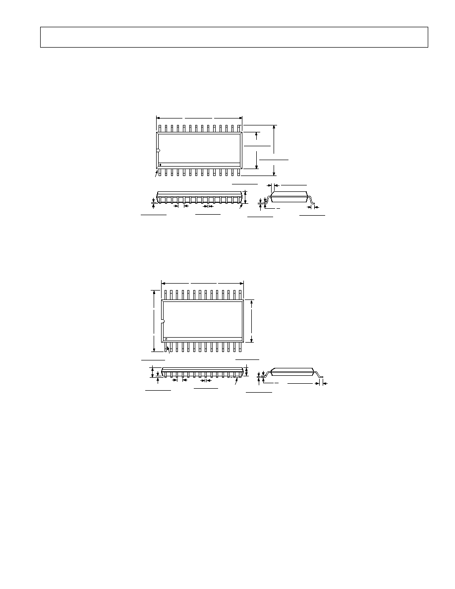
OUTLINE DIMENSIONS
Dimensions shown in inches and (mm).
28-Lead, 300 Mil SOIC
(R-28)
0.0125 (0.32)
0.0091 (0.23)
8
0
0.0291 (0.74)
0.0098 (0.25)
45
0.0500 (1.27)
0.0157 (0.40)
SEATING
PLANE
0.0118 (0.30)
0.0040 (0.10)
0.0192 (0.49)
0.0138 (0.35)
0.1043 (2.65)
0.0926 (2.35)
0.0500
(1.27)
BSC
28
15
14
1
0.7125 (18.10)
0.6969 (17.70)
0.4193 (10.65)
0.3937 (10.00)
0.2992 (7.60)
0.2914 (7.40)
PIN 1
28-Lead, 5.33 mm SSOP
(RS-28)
0.009 (0.229)
0.005 (0.127)
0.03 (0.762)
0.022 (0.558)
8°
0°
0.008 (0.203)
0.002 (0.050)
0.07 (1.79)
0.066 (1.67)
0.078 (1.98)
0.068 (1.73)
0.015 (0.38)
0.010 (0.25)
SEATING
PLANE
0.0256
(0.65)
BSC
0.311 (7.9)
0.301 (7.64)
0.212 (5.38)
0.205 (5.21)
28
15
14
1
0.407 (10.34)
0.397 (10.08)
PIN 1
C3700a012/99 (rev. A)
PRINTED IN U.S.A.