 | ÐлекÑÑоннÑй компоненÑ: AD9805 | СкаÑаÑÑ:  PDF PDF  ZIP ZIP |
Äîêóìåíòàöèÿ è îïèñàíèÿ www.docs.chipfind.ru
REV. 0
Information furnished by Analog Devices is believed to be accurate and
reliable. However, no responsibility is assumed by Analog Devices for its
use, nor for any infringements of patents or other rights of third parties
which may result from its use. No license is granted by implication or
otherwise under any patent or patent rights of Analog Devices.
a
AD9807/AD9805
One Technology Way, P.O. Box 9106, Norwood, MA 02062-9106, U.S.A.
Tel: 617/329-4700
World Wide Web Site: http://www.analog.com
Fax: 617/326-8703
© Analog Devices, Inc., 1997
Complete 12-Bit/10-Bit 6 MSPS
CCD/CIS Signal Processors
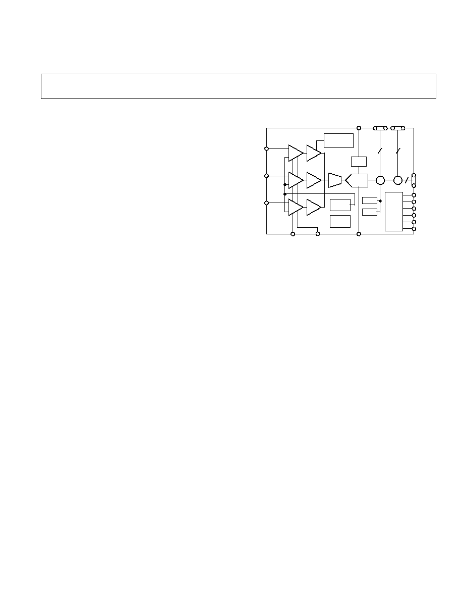
FUNCTIONAL BLOCK DIAGRAM
PGA
PGA
PGA
GREEN
RED
BLUE
MUX
ADC
REF
GAIN
REGISTERS
INPUT
OFFSET
CONFIG
REGS
ODD
EVEN
8-10
12-10
12-10
MPU
PORT
CSB
RD
WR
A2
A1
A0
VREF
PIXEL
OFFSET
PIXEL
GAIN
CDSCLK1
CDSCLK2
ADCCLK
VINR
VING
VINB
DOUT
AD9807/AD9805
PGA
PGA
GAIN
REGISTERS
MUX
REF
INPUT
OFFSET
CONFIG
REGS
EVEN
ODD
MPU
PORT
X
CDS
CDS
CDS
PRODUCTION DESCRIPTION
The AD9807 and AD9805 are complete CCD/CIS imaging
decoders and signal processors on a single monolithic integrated
circuit. The input of the AD9807/AD9805 allows direct ac
coupling of the charge-coupled device (CCD) or contact image
sensor (CIS) output(s). The AD9807/AD9805 includes all the
circuitry to perform three-channel correlated double sampling
(CDS) and programmable gain adjustment of the CCD output;
a 12-bit or 10-bit analog-to-digital converter (ADC) quantizes
the analog signal. After digitization, the on-board digital signal
processor (DSP) circuitry allows pixel rate offset and gain correc-
tion. The DSP also corrects odd/even CCD register imbalance
errors. A parallel control bus provides a simple interface to
8-bit microcontrollers. The AD9807/AD9805 comes in a
space saving 64-pin plastic quad flatpack (PQFP) and is specified
over the commercial (0
°
C to +70
°
C) temperature range. By
disabling the CDS, the AD9807/AD9805 are also suitable for
non-CCD applications, or applications that do not require
CDS, such as CIS signal processing.
PRODUCT HIGHLIGHTS
The AD9807/AD9805 offers a complete, single chip CCD
imaging front end in a 64-pin plastic quad flatpack (PQFP).
On-Chip PGA--The AD9807/AD9805 includes a 3-channel
analog programmable gain amplifier; it is programmable from
1
×
to 4
×
in 16 increments.
On-Chip CDS--An integrated 3-channel correlated double
sampler allows easy ac coupling directly from the CCD sensor
outputs. Additionally, the CDS reduces low frequency noise
and reset feedthrough.
On-Chip Voltage Reference--The AD9807/AD9805 includes a
2 V bandgap reference that allows the input range of the device to
be configured for input spans up to 4 V.
6 MSPS A/D Converter--A highly linear 12-bit or 10-bit A/D
converter sequentially digitizes the red, green and blue CDS
outputs ensuring no missing code performance. The user may also
configure the AD9807/AD9805 for single channel operation.
Digital Gain & Offset Correction--Pixel rate digital gain and
offset correction blocks allow precise repeatable correction of
imaging system error sources.
Digital I/O Compatibility--The AD9807/AD9805 offers
+3.3 V/+5 V logic level compatibility.
Pin-Compatible 12-Bit and 10-Bit Versions--The AD9807 is
also offered in a pin-compatible 10-bit version, the AD9805,
allowing upgrade-ability and simplifying design issues across
different scanner models.
FEATURES
Pin Compatible 12-Bit and 10-Bit Versions
12-Bit/10-Bit 6 MSPS A/D Converter
Integrated Triple Correlated Double Sampler
3-Channel, 2 MSPS Color Mode
1 4 Analog Programmable Gain Amplifier
Pixel-Rate Digital Gain Adjustment
Pixel-Rate Digital Offset Adjustment
Internal Voltage Reference
No Missing Codes Guaranteed
Microprocessor-Compatible Control Interface
+3.3 V/+5 V Digital I/O Compatibility
Low Power CMOS: 500 mW
64-Pin PQFP Surface Mount Package
2
REV. 0
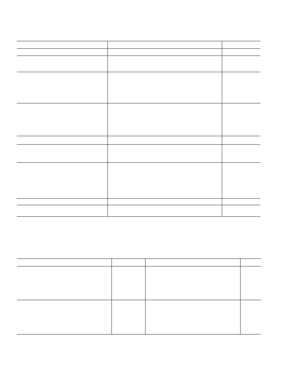
Parameter
Min
Typ
Max
Units
RESOLUTION
12
Bits
CONVERSION RATE
3-Channel Mode With CDS
6
MSPS
1-Channel Mode With CDS
1
6
MSPS
DC ACCURACY
Integral Nonlinearity (INL)
2
1.5
LSB
Differential Nonlinearity (DNL)
2
0.4
0.75
LSB
No Missing Codes
12
Bits Guaranteed
Unipolar Offset Error (@ +25
°
C)
0.4
% FSR
Gain Error (@ +25
°
C)
1.2
% FSR
ANALOG INPUTS
Full-Scale Input Span
0.0625
4
V p-p
Input Limits
3
AV
SS
0.3 V
AV
DD
+ 0.3
V
Input Capacitance
10
pF
Input Bias Current
0.01
µ
A
Input Referred Noise
0.3
LSB rms
PSRR (AV
DD
= +5 V
±
0.25 V)
0.06
% FSR
INTERNAL VOLTAGE REFERENCE
1 V Output Tolerance (@+25
°
C)
±
15
mV
2 V Output Tolerance (@+25
°
C)
±
30
mV
POWER SUPPLIES
Operating Voltages
AV
DD
+4.75
+5.25
V
DV
DD
+4.75
+5.25
V
Operating Current
AV
DD
73
86
mA
DV
DD
16.6
20
mA
POWER CONSUMPTION
450
530
mW
TEMPERATURE RANGE
Operating
0
+70
°
C
NOTES
1
Blue and green channels. Red channel conversion rate for 1-channel mode is 5 MSPS.
2
Measured with 4 V p-p input range.
3
Input signals exceeding these limits are subject to excessive overvoltage recovery times.
Specifications subject to change without notice.
ANALOG SPECIFICATIONS
DIGITAL SPECIFICATIONS
Parameter
Symbol
Min
Typ
Max
Units
LOGIC INPUTS
High Level Input Voltage
V
IH
2.0
V
Low Level Input Voltage
V
IL
0.8
V
High Level Input Current
I
IH
10
µ
A
Low Level Input Current
I
IL
10
µ
A
Input Capacitance
C
IN
10
pF
LOGIC OUTPUTS
High Level Output Voltage (I
OH
= 50
µ
A)
V
OH
4.5
4.9
V
High Level Output Voltage (I
OH
= 0.5 mA)
V
OH
2.4
V
Low Level Output Voltage (I
OL
= 50
µ
A)
V
OL
0.1
V
Low Level Output Voltage (I
OL
= 0.6 mA)
V
OL
0.4
V
Output Capacitance
C
OUT
5
pF
Specifications subject to change without notice.
(T
MIN
to T
MAX
with AV
DD
= +5.0 V, DV
DD
= +5.0 V, f
ADCCLK
= 6 MSPS, f
CDSCLK1
= 2 MSPS, f
CDSCLK2
= 2 MSPS,
C
L
= 20 pF, unless otherwise noted)
(T
MIN
to T
MAX
with AV
DD
= +5.0 V, DV
DD
= +5.0 V, f
ADCCLK
= 6 MSPS, f
CDSCLK1
= 2 MSPS, f
CDSCLK2
= 2 MSPS,
PGA Gain = 1 unless otherwise noted)
AD9807SPECIFICATIONS
3
REV. 0
AD9807/AD9805
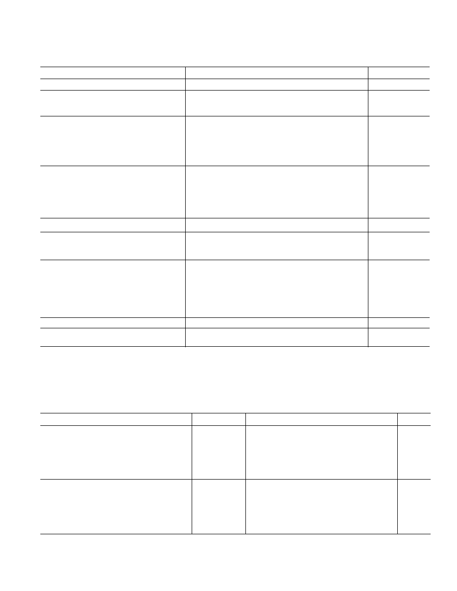
Parameter
Min
Typ
Max
Units
RESOLUTION
10
Bits
CONVERSION RATE
3-Channel Mode With CDS
6
MSPS
1-Channel Mode With CDS
1
6
MSPS
DC ACCURACY
Integral Nonlinearity (INL)
2
1.0
LSB
Differential Nonlinearity (DNL)
2
0.5
LSB
No Missing Codes
10
Bits Guaranteed
Unipolar Offset Error (@ +25
°
C)
0.6
% FSR
Gain Error (@ +25
°
C)
1.2
% FSR
ANALOG INPUTS
Full-Scale Input Span
0.0625
4
V p-p
Input Limits
3
AV
SS
0.3 V
AV
DD
+ 0.3
V
Input Capacitance
10
pF
Input Bias Current
0.01
µ
A
Input Referred Noise
0.1
LSB rms
PSRR (AV
DD
= +5 V
±
0.25 V)
0.06
% FSR
INTERNAL VOLTAGE REFERENCE
1 V Output Tolerance (@ +25
°
C)
±
15
mV
2 V Output Tolerance (@ +25
°
C)
±
30
mV
POWER SUPPLIES
Operating Voltages
AV
DD
+4.75
+5.25
V
DV
DD
+4.75
+5.25
V
Operating Current
AV
DD
73
86
mA
DV
DD
16.6
20
mA
POWER CONSUMPTION
450
530
mW
TEMPERATURE RANGE
Operating
0
+70
°
C
NOTES
1
Blue and green channels. Red channel conversion rate for 1-channel mode is 5 MSPS.
2
Measured with 4 V p-p input range.
3
Input signals exceeding these limits are subject to excessive overvoltage recovery times.
Specifications subject to change without notice.
ANALOG SPECIFICATIONS
DIGITAL SPECIFICATIONS
Parameter
Symbol
Min
Typ
Max
Units
LOGIC INPUTS
High Level Input Voltage
V
IH
2.0
V
Low Level Input Voltage
V
IL
0.8
V
High Level Input Current
I
IH
10
µ
A
Low Level Input Current
I
IL
10
µ
A
Input Capacitance
C
IN
10
pF
LOGIC OUTPUTS
High Level Output Voltage (I
OH
= 50
µ
A)
V
OH
4.5
4.9
V
High Level Output Voltage (I
OH
= 0.5 mA)
V
OH
2.4
V
Low Level Output Voltage (I
OL
= 50
µ
A)
V
OL
0.1
V
Low Level Output Voltage (I
OL
= 0.6 mA)
V
OL
0.4
V
Output Capacitance
C
OUT
5
pF
Specifications subject to change without notice.
(T
MIN
to T
MAX
with AV
DD
= +5.0 V, DV
DD
= +5.0 V, f
ADCCLK
= 6 MSPS, f
CDSCLK1
= 2 MSPS, f
CDSCLK2
= 2 MSPS,
C
L
= 20 pF, unless otherwise noted)
(T
MIN
to T
MAX
with AV
DD
= +5.0 V, DV
DD
= +5.0 V, f
ADCCLK
= 6 MSPS, f
CDSCLK1
= 2 MSPS, f
CDSCLK2
= 2 MSPS,
PGA Gain = 1 unless otherwise noted)
AD9805SPECIFICATIONS
AD9807/AD9805
4
REV. 0
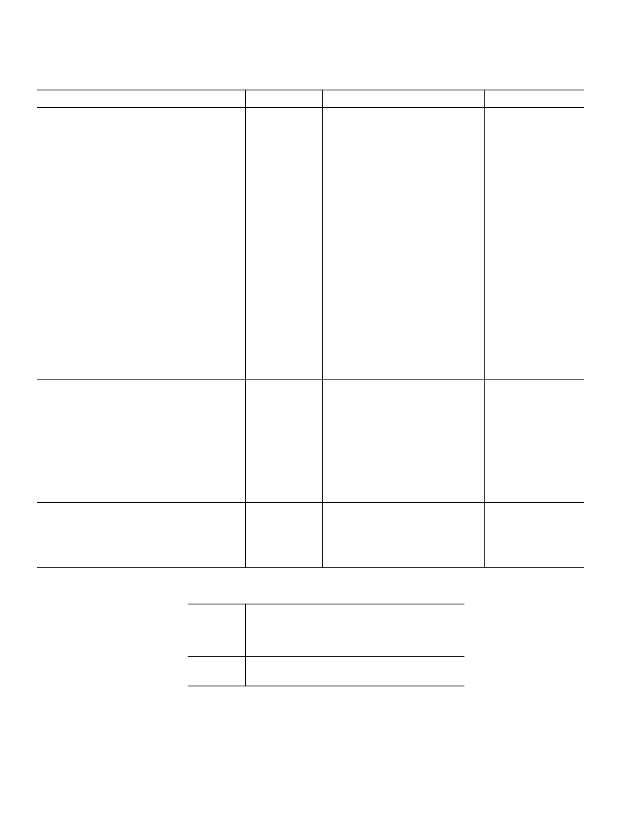
TIMING SPECIFICATIONS
Parameter
Symbol
Min
Typ
Max
Units
CLOCK PARAMETERS
3-Channel Conversion Rate
t
CRA
500
ns
1-Channel Conversion Rate
t
CRB
166
ns
CDSCK1 Pulse Width
t
C1A
30
ns
CDSCK1 Pulse Width
t
C1B
30
ns
CDSCK2 Pulse Width
t
C2A
30
ns
CDSCK2 Pulse Width
t
C2B
30
ns
CDS Clocks Digital Quiet Time
t
Q
20
ns
CDSCK2 Falling to CDSCK1 Rising
t
C2C1A
80
ns
CDSCK2 Falling to CDSCK1 Rising
t
C2C1B
40
ns
CDSCK1 Falling to CDSCK2 Rising
t
C1C2A
20
ns
CDSCK1 Falling to CDSCK2 Rising
t
C1C2B
20
ns
ADCCLK Rising to CDSCK1 Falling
t
C1AD
35
ns
ADCCLK Pulse Width
t
ACLK
50
ns
ADCCLK Period
t
CP
166
ns
ADCCLK Period (Red Single Channel Mode)
t
CP2
200
ns
3-Channel Settling Time
t
STL1
60
ns
1-Channel Settling Time (B and G Only)
t
STL2
30
ns
ADCCLK Rising to Control Data Setup
t
GOS
15
ns
ADCCLK Rising to Control Data Hold
t
GOH
15
ns
STRTLN Rising, Falling Setup
t
S
15
ns
STRTLN Rising, Falling Hold
t
H
15
ns
Aperture Delay
t
AD
10
ns
REGISTER WRITE/READ
Address Setup Time
t
AS
15
ns
Address Hold Time
t
AH
15
ns
Data Setup Time
t
DS
15
ns
Data Hold Time
t
DH
15
ns
Chip Select Setup Time
t
CSS
15
ns
Chip Select Hold Time
t
CSH
15
ns
Write Pulse Width
t
PWW
25
ns
Read Pulse Width
t
PWR
50
ns
Read To Data Valid
t
DD
40
ns
DATA OUTPUT
Output Delay
t
OD
15
ns
3-State to Data Valid
t
EDV
15
ns
Output Enable High to 3-State
t
HZ
5
ns
Latency
6
ADCCLK Cycles
(T
MIN
to T
MAX
with AV
DD
= +5.0 V, DV
DD
= +5.0 V, unless otherwise noted)
Table I. Output Controls
CSB
0
0
0
0
0
0
1
1
RDB
0
0
1
1
1
1
x
x
WRB
0
1
0
0
1
1
x
x
OEB
x
x
0
1
0
1
0
1
DOUT
X
Q
X
D
X
Z
Q
Z
MPU
MPU
ADC
LEGEND:
x = Don't Care
X = Unknown (Not Recommended)
Q = Outputs
D = Inputs
Z = 3-State
AD9807/AD9805
5
REV. 0
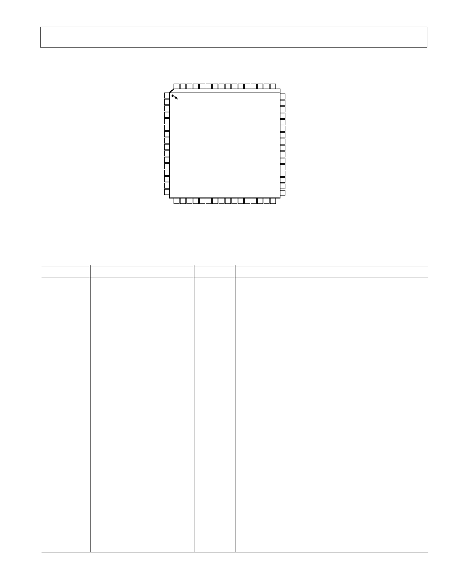
PIN CONFIGURATION
1
2
3
4
5
6
7
8
9
10
11
13
14
15
16
12
17 18 19 20 21 22 23 24 25 26 27 28 29 30 31 32
48
47
46
45
44
43
42
41
40
39
38
37
36
35
34
33
64 63 62 61 60
55 54 53 52 51 50 49
59 58 57 56
PIN 1
IDENTIFIER
TOP VIEW
(Not to Scale)
GAIN<11>
GAIN<10>
GAIN<9>
GAIN<8>
GAIN<7>
GAIN<6>
GAIN<5>
GAIN<4>
GAIN<3>
GAIN<2>
GAIN<1>
GAIN<0>
DVSS
DVDD
A2
A1
AVDD
AVSS
CAPT
CAPT
CAPB
CAPB
VREF
CML
VINR
AVSS
VING
AVSS
VINB
AVSS
AVDD
STRTLN
A0
DOUT<11>
DOUT<10>
DOUT<9>
DOUT<8>
DOUT<7>/MPU<7>
DOUT<6>/MPU<6>
DRVDD
DRVSS
DOUT<5>/MPU<5>
DOUT<4>/MPU<4>
DOUT<3>/MPU<3>
DOUT<2>/MPU<2>
DOUT<1>/MPU<1>
DOUT<0>/MPU<0>
OEB
CDSCLK1
CDSCLK2
ADCCLK
OFFSET<7>
OFFSET<6>
OFFSET<5>
OFFSET<4>
OFFSET<3>
OFFSET<2>
OFFSET<1>
DVSS
DVDD
CSB
RDB
WRB
OFFSET<0>
AD9807
PIN DESCRIPTIONS
Pin No.
Pin Name
Type
Description
1, 15
AVDD
P
+5 V Analog Supply.
2, 10, 12, 14
AVSS
P
Analog Ground.
3, 4
CAPT
AO
Reference Decoupling. See Figure 22.
5, 6
CAPB
AO
Reference Decoupling.
7
VREF
AO
Internal Reference Output. Decouple with 10
µ
F + 0.1
µ
F.
8
CML
AO
Internal Bias Voltage. Decouple with 0.1
µ
F.
9
VINR
AI
Analog Input, Red.
11
VING
AI
Analog Input, Green.
13
VINB
AI
Analog Input, Blue.
16
STRTLN
DI
STRTLN. Indicates beginning of scan line.
17
CDSCLK1
DI
CDS Reset Clock Pulse Input.
18
CDSCLK2
DI
CDS Data Clock Pulse Input.
19
ADCCLK
DI
A/D Sample Clock Input.
28, 52
DVSS
P
Digital Ground.
29, 51
DVDD
P
+5 V Digital Supply.
20
OFFSET<7>
DI
Pixel Rate Offset Coefficient Inputs. Most Significant Bit.
2126
OFFSET<6:1>
DI
Pixel Rate Offset Coefficient Inputs.
27
OFFSET<0>
DI
Pixel Rate Offset Coefficient Inputs. Least Significant Bit.
30
CSB
DI
Chip Select. Active Low.
31
RDB
DI
Read Strobe. Active Low.
32
WRB
DI
Write Strobe. Active Low.
33
OEB
DI
Output Enable. Active Low.
34
DOUT<0>/MPU<0>
DIO
Data Output LSB/Register Input LSB
3539, 42
DOUT<1:6>/MPU<1:6>
DIO
Data Outputs/Register Inputs.
40
DRVSS
P
Digital Driver Ground
41
DRVDD
P
Digital Driver Supply
43
DOUT<7>/MPU<7>
DIO
Data Output/Register Input MSB.
4446
DOUT<8:10>
DO
Data Outputs.
47
DOUT<11>
DO
Data Output MSB.
48, 49, 50
A0, A1, A2
DI
Register Select Pins.
53
GAIN<0>
DI
Pixel Rate Gain Coefficient Input. LSB.
5463
GAIN<1:10>
DI
Pixel Rate Gain Coefficient Inputs.
64
GAIN<11>
DI
Pixel Rate Gain Coefficient Input. MSB.
TYPE: AI = Analog Input; AO = Analog Output; DI = Digital Input; DO = Digital Output; DIO = Digital Input/Output; P = Power.
AD9807/AD9805
6
REV. 0
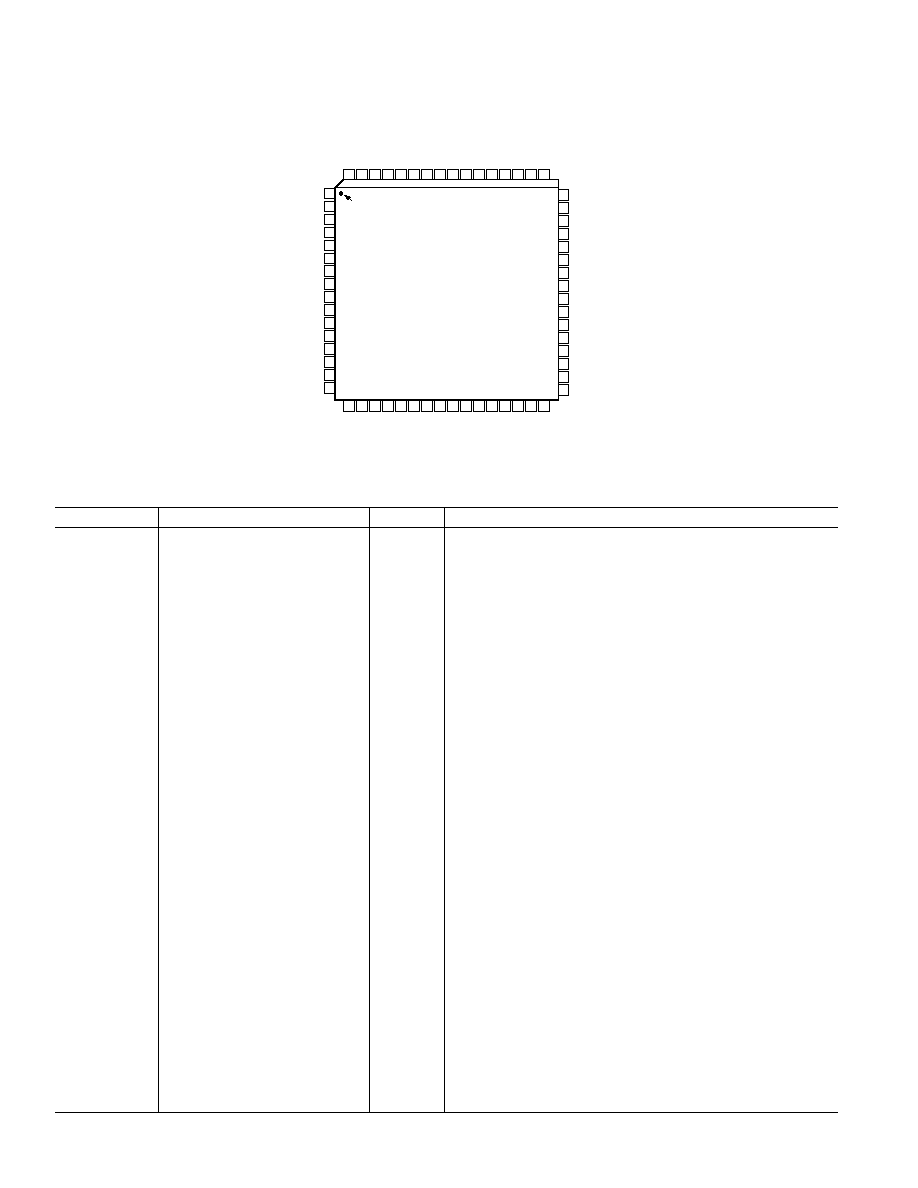
PIN CONFIGURATION
1
2
3
4
5
6
7
8
9
10
11
13
14
15
16
12
17 18 19 20 21 22 23 24 25 26 27 28 29 30 31 32
48
47
46
45
44
43
42
41
40
39
38
37
36
35
34
33
64 63 62 61 60
55 54 53 52 51 50 49
59 58 57 56
PIN 1
IDENTIFIER
TOP VIEW
(Not to Scale)
GAIN<9>
GAIN<8>
GAIN<7>
NC
GAIN<6>
GAIN<5>
GAIN<4>
GAIN<3>
GAIN<2>
GAIN<1>
GAIN<0>
DVSS
DVDD
A2
A1
AVDD
AVSS
CAPT
CAPT
CAPB
CAPB
VREF
CML
VINR
AVSS
VING
AVSS
VINB
AVSS
AVDD
STRTLN
A0
DOUT<9>
DOUT<8>
DOUT<7>
DOUT<6>
DOUT<5>/MPU<7>
DOUT<4>/MPU<6>
DRVDD
DRVSS
DOUT<3>/MPU<5>
DOUT<2>/MPU<4>
DOUT<1>/MPU<3>
DOUT<0>/MPU<2>
MPU<1>
MPU<0>
OEB
CDSCLK1
CDSCLK2
ADCCLK
OFFSET<7>
OFFSET<6>
OFFSET<5>
OFFSET<4>
OFFSET<3>
OFFSET<2>
OFFSET<1>
DVSS
DVDD
CSB
RDB
WRB
OFFSET<0>
AD9805
NC
NC = NO CONNECT
PIN DESCRIPTIONS
Pin No.
Pin Name
Type
Description
1, 15
AVDD
P
+5 V Analog Supply.
2, 10, 12, 14
AVSS
P
Analog Ground.
3, 4
CAPT
AO
Reference Decoupling. See Figure 22.
5, 6
CAPB
AO
Reference Decoupling.
7
VREF
AO
Internal Reference Output. Decouple with 10
µ
F + 0.1
µ
F.
8
CML
AO
Internal Bias Voltage. Decouple with 0.1
µ
F.
9
VINR
AI
Analog Input, Red.
11
VING
AI
Analog Input, Green.
13
VINB
AI
Analog Input, Blue.
16
STRTLN
DI
STRTLN. Indicates beginning of scan line.
17
CDSCLK1
DI
CDS Reset Clock Pulse Input.
18
CDSCLK2
DI
CDS Data Clock Pulse Input.
19
ADCCLK
DI
A/D Sample Clock Input.
28, 52
DVSS
P
Digital Ground.
29, 51
DVDD
P
+5 V Digital Supply.
20
OFFSET<7>
DI
Pixel Rate Offset Coefficient Inputs. Most Significant Bit.
2126
OFFSET<6:1>
DI
Pixel Rate Offset Coefficient Inputs.
27
OFFSET<0>
DI
Pixel Rate Offset Coefficient Inputs. Least Significant Bit.
30
CSB
DI
Chip Select. Active Low.
31
RDB
DI
Read Strobe. Active Low.
32
WRB
DI
Write Strobe. Active Low.
33
OEB
DI
Output Enable. Active Low.
34
MPU<0>
DIO
Register Input-Output LSB.
35
MPU<1>
DIO
Register Input-Output.
36
DOUT<0>/MPU<2>
DIO
Data Output LSB/Register Input-Output.
3739, 42
DOUT<1:4>/MPU<3:6>
DIO
Data Output/Register Input-Output.
40
DRVSS
P
Digital Driver Ground.
41
DRVDD
P
Digital Driver Supply.
43
DOUT<5>/MPU<7>
DIO
Data Output/Register Input-Output MSB.
4446
DOUT<6:8>
DO
Data Outputs.
47
DOUT<9>
DO
Data Output MSB.
48, 49, 50
A0, A1, A2
DI
Register Select Pins.
53, 54
NC
No Connection.
55
GAIN<0>
DI
Pixel Rate Gain Coefficient Input LSB.
5663
GAIN<1:8>
DI
Pixel Rate Gain Coefficient Inputs.
64
GAIN<9>
DI
Pixel Rate Gain Coefficient Input MSB.
TYPE: AI = Analog Input; AO = Analog Output; DI = Digital Input; DO = Digital Output; DIO = Digital Input/Output; P = Power.
AD9807/AD9805
7
REV. 0
WARNING!
ESD SENSITIVE DEVICE
CAUTION
ESD (electrostatic discharge) sensitive device. Electrostatic charges as high as 4000 V readily
accumulate on the human body and test equipment and can discharge without detection.
Although the AD9807/AD9805 feature proprietary ESD protection circuitry, permanent damage
may occur on devices subjected to high energy electrostatic discharges. Therefore, proper ESD
precautions are recommended to avoid performance degradation or loss of functionality.
ABSOLUTE MAXIMUM RATINGS*
With
Respect
Parameter
to
Min
Max
Units
AVDD
AVSS
0.5
+6.5
Volts
AVSS
AVDD
6.5
+0.5
Volts
DVDD
DVSS
0.5
+6.5
Volts
AGND
DVSS
0.3
+0.3
Volts
AVDD
DVDD
6.5
+6.5
Volts
Clock Input
DVSS
0.5
DVDD + 0.5 Volts
Digital Outputs
DVSS
0.5
AVDD + 0.3 Volts
AIN, VREF
AVSS
0.3
AVDD + 0.3 Volts
Junction Temperature
+150
°
C
Storage Temperature
65
+150
°
C
Lead Temperature (10 sec)
+300
°
C
*Stresses above those listed under "Absolute Maximum Ratings" may cause
permanent damage to the device. This is a stress rating only; functional operation
of the device at these or any other conditions above those indicated in the
operational sections of this specification is not implied. Exposure to absolute
maximum ratings for extended periods may affect device reliability.
ORDERING GUIDE
Temperature
Package
Package
Model
Range
Description
Option*
AD9807JS
0
°
C to +70
°
C
PQFP
S-64
AD9805JS
0
°
C to +70
°
C
PQFP
S-64
*S = Plastic Quad Flatpack.
DEFINITIONS OF SPECIFICATIONS
INTEGRAL NONLINEARITY
Linearity error refers to the deviation of each individual code
from a line drawn from "negative full scale" through "positive
full scale." The point used as "negative full scale" occurs
1/2 LSB
before the first code transition. "Positive full scale" is defined as a
level 1 1/2 LSB beyond the last code transition. The deviation is
measured from the middle of each particular code to the true
straight line.
DIFFERENTIAL LINEARITY ERROR (DNL, NO MISSING
CODES)
An ideal ADC exhibits code transitions that are exactly 1 LSB
apart. DNL is the deviation from this ideal value. Thus every
code must have a finite width. Guaranteed no missing codes
to 12-bit resolution indicates that all 4096 codes, respectively,
must be present over all operating ranges.
UNIPOLAR OFFSET ERROR
In the unipolar mode, the first transition should occur at a level
1/2 LSB above analog common. Unipolar offset is defined as
the deviation of the actual from that point. The unipolar offset
temperature coefficient specifies the maximum change of the
transition point over temperature, with or without external
adjustments.
GAIN ERROR
The last transition should occur for an analog value 1 1/2 LSB
below the nominal full scale. Gain error is the deviation of the
actual difference between first and last code transitions and the
ideal difference between first and last code transitions.
POWER SUPPLY REJECTION
Power Supply Rejection specifies the maximum full-scale change
from the initial value with the supplies at the various limits.
APERTURE DELAY
Aperture delay is a timing measurement between the sampling
clocks and the CDS. It is measured from the falling edge of the
CDSCLK2 input to when the input signal is held for conversion
in CDS mode. In non-CDS mode, it is the falling edge of
CDSCLK1.
AD9807/AD9805
8
REV. 0
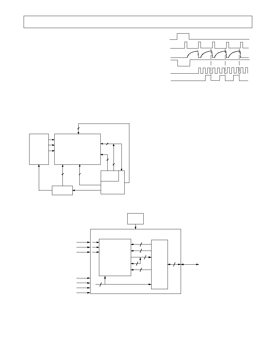
R0, G0, B0
R1, G1, B1
Rn, Gn, Bn
t
AD
t
AD
t
C1A
t
C2C1A
t
CRA
t
S
t
H
t
GOH
t
GOS
t
CP2
t
C1AD
t
ACLK
t
ACLK
t
STL1
R
G
B
R
G
B
R
G
B
ANALOG
INPUTS
STRTLN
CDSCLK1
CDSCLK2
ADCCLK
GAIN<n:0>
OFFSET<m:0>
R0
G0
B0
R1
G1
B1
t
C2A
t
C1C2A
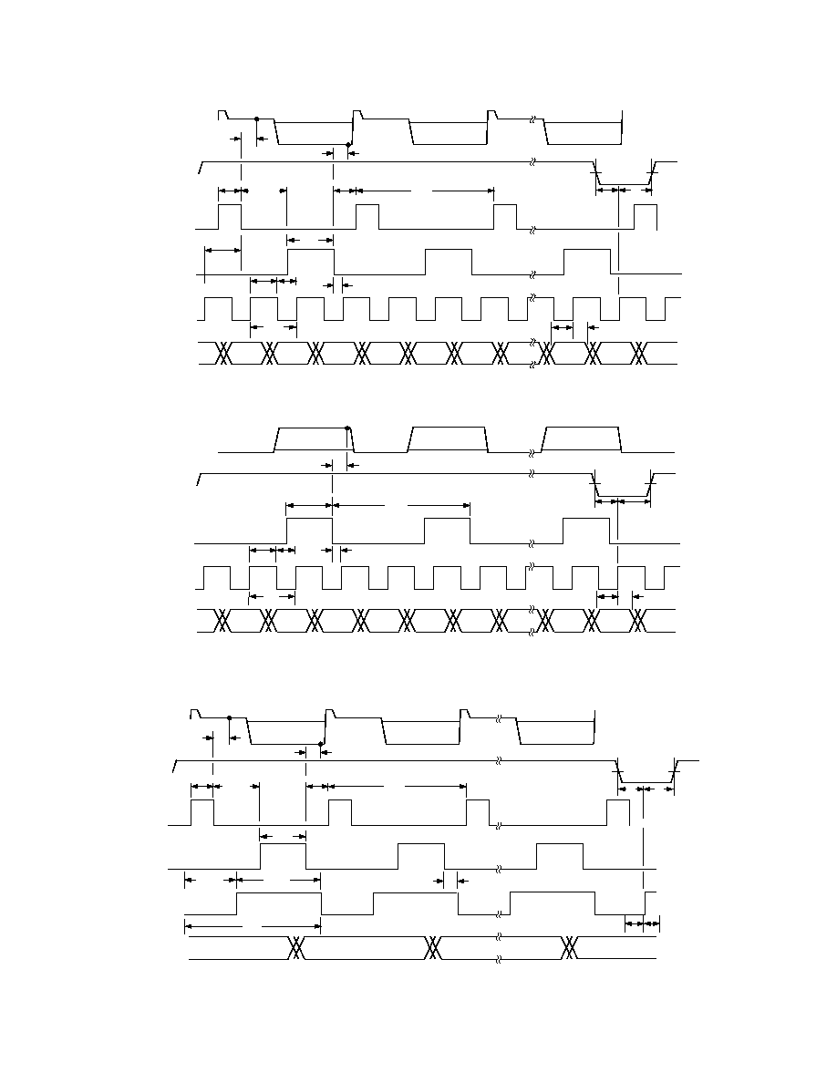
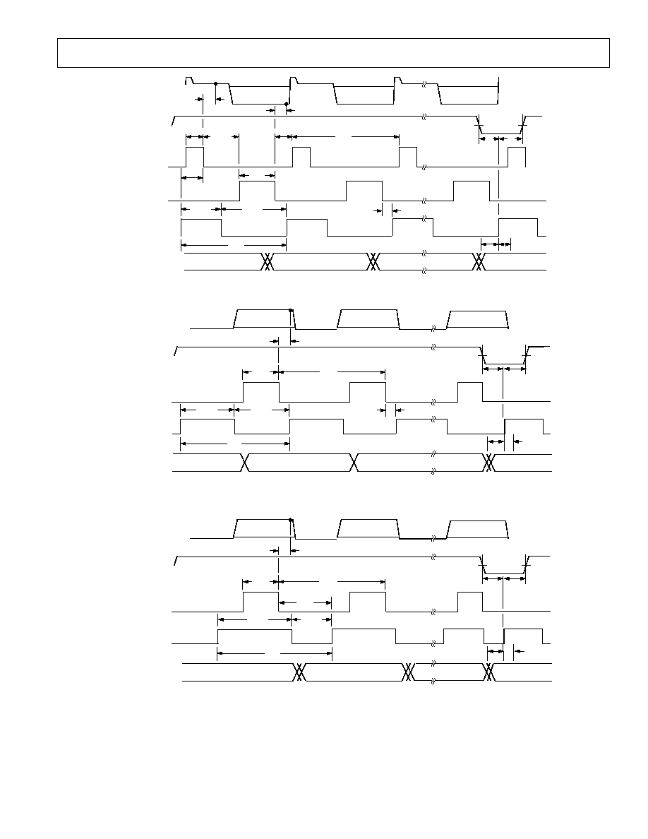
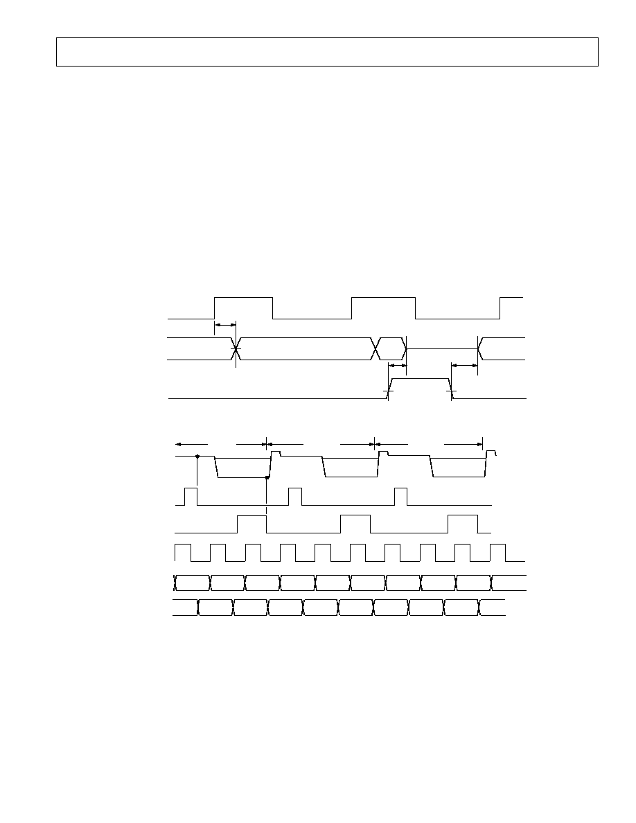
Figure 1a. 3-Channel CDS-Mode Clock Timing
t
GOH
t
GOS
t
CP
t
C2A
t
ACLK
t
ACLK
t
STL1
CDSCLK1
ADCCLK
GAIN<n:0>
OFFSET<m:0>
t
CRA
t
S
t
H
STRTLN
t
AD
(0V)
ANALOG
INPUTS
R0, G0, B0
R1, G1, B1
Rn, Gn, Bn
Figure 1b. 3-Channel SHA-Mode Clock Timing
PIXEL 0
t
S
t
H
t
GOH
t
GOS
t
C1B
t
C2C1B
t
CRB
CDSCLK1
t
C1C2B
PIXEL 1
PIXEL n
t
AD
t
AD
ANALOG
INPUTS
STRTLN
CDSCLK2
t
ACLK
t
ACLK
G2
G1
G0
t
CP
ADCCLK
GAIN<n:0>
OFFSET<m:0>
t
C2B
t
STL2
Figure 1c. 1-Channel CDS-Mode Clock Timing (for B and G Only)
AD9807/AD9805
9
REV. 0
PIXEL 0
t
S
t
H
t
GOH
t
GOS
t
C1B
t
C2C1B
t
CRB
CDSCLK1
t
C1C2B
t
C1AD
PIXEL 1
PIXEL n
t
AD
t
AD
ANALOG
INPUTS
STRTLN
CDSCLK2
t
STL1
t
ACLK
t
ACLK
G2
G1
G0
t
CP2
ADCCLK
GAIN<n:0>
OFFSET<m:0>
t
C2B
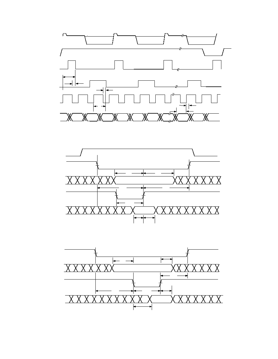
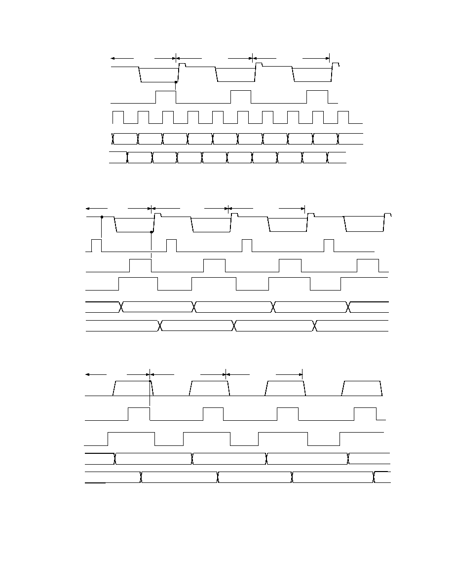
Figure 1d. 1-Channel CDS-Mode Clock Timing (Red Channel)
CDSCLK1
t
CRB
t
S
t
H
STRTLN
Rn, Gn, Bn
t
AD
(0V)
ANALOG
INPUTS
R0, G0, B0
R1, G1, B1
t
C2B
t
ACLK
t
ACLK
t
STL2
t
CP
t
GOS
t
GOH
G1
G0
ADCCLK
GAIN<n:0>
OFFSET<m:0>
G2
Figure 1e. 1-Channel SHA-Mode Clock Timing (for Blue and Green Channels)
CDSCLK1
t
CRB
t
S
t
H
STRTLN
Rn, Gn, Bn
t
AD
(0V)
ANALOG
INPUTS
R0, G0, B0
R1, G1, B1
t
C2B
t
ACLK
t
ACLK
t
CP2
t
GOS
t
GOH
G1
G0
ADCCLK
GAIN<n:0>
OFFSET<m:0>
t
STL1
Figure 1f. 1-Channel SHA-Mode Clock Timing (Red Channel)
AD9807/AD9805
10
REV. 0
t
PWR
t
AS
t
AH
t
CSS
t
CSH
t
DD
t
DH
CSB
A0, A1, A2
RDB
MPU<7:0>
Figure 3. Read Timing
R
G
B
R
G
B
R
G
B
CDSCLK1
STRTLN
Rn, Gn, Bn
ANALOG
INPUTS
R0, G0, B0
R1, G1, B1
B1
R0
G0
B0
R1
G1
ADCCLK
GAIN<n:0>
OFFSET<m:0>
t
Q
t
Q
CDSCLK2
t
Q
t
GOS
t
GOH
t
Q
Figure 1g. CDS Clocks Digital Quiet Time
t
PWW
t
AS
t
AH
t
CSS
t
CSH
t
DS
t
DH
OEB
CSB
A0, A1, A2
WRB
MPU<7:0>
Figure 2. Write Timing
AD9807/AD9805
11
REV. 0
7
6
5
4
3
2
1
0
8X FULL SCALE
4X FULL SCALE
2X FULL SCALE
10-BIT GAIN, 10-BIT OFFSET
11-BIT GAIN, 9-BIT OFFSET
12-BIT GAIN, 8-BIT OFFSET
COLOR0
COLOR1
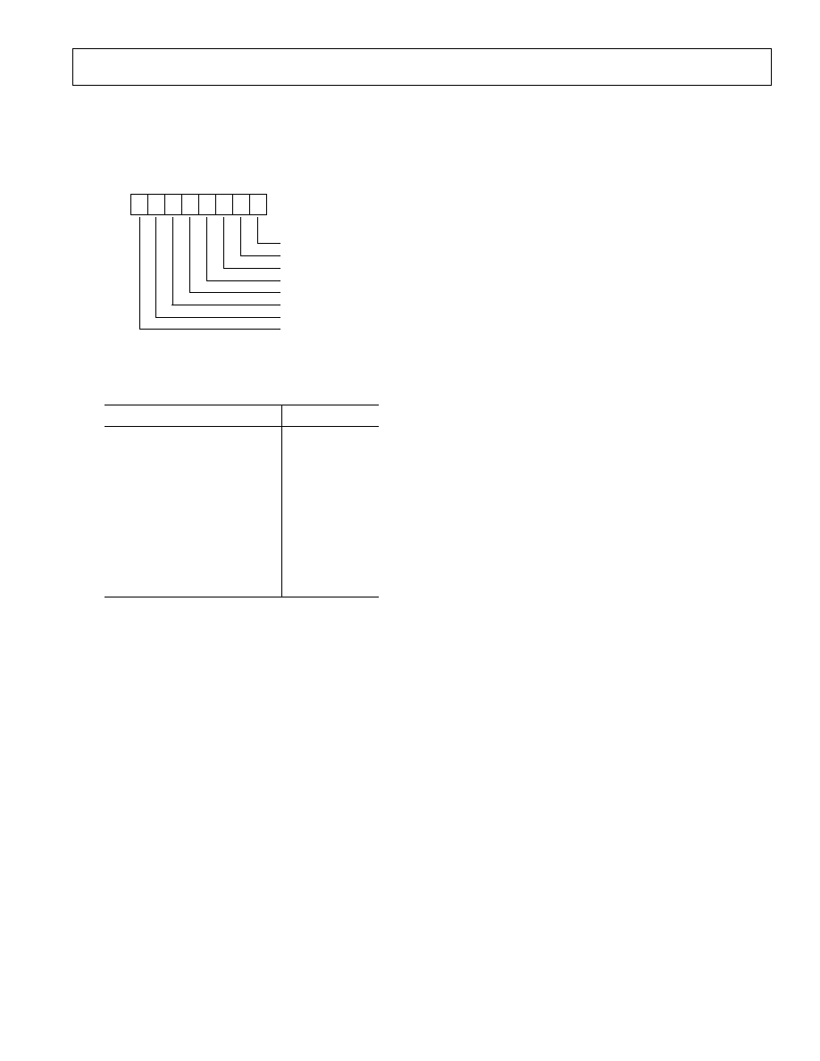
Figure 5. AD9807 Configuration Register Format
Configuration Register/AD9805
The Configuration Register controls three functions: a color
pointer, gain and offset pin configurations, and digital gain
scaling. Figure 6 shows the AD9805 Configuration Register.
Bits 02 control the digital scaling function. Setting a Bit
makes the corresponding condition true. Resetting Bits 02
disables and bypasses the digital multiplier. Bits 35 control
the gain and offset pin distribution. Resetting Bits 35 disables
and bypasses the digital subtracter and sets the gain word width
to 10. Setting any bit makes the corresponding condition true.
If Bit 3 is set, the 2 LSBs of the gain word become the 2 MSBs
of the offset word. If Bit 4 is set, the LSB of the gain word
becomes MSB of the offset word. Bits 6 and 7 direct register
data written to the MPU<7:0> bus to the appropriate red,
green or blue register.
7
6
5
4
3
2
1
0
8X FULL SCALE
4X FULL SCALE
2X FULL SCALE
8-BIT GAIN, 10-BIT OFFSET
9-BIT GAIN, 9-BIT OFFSET
10-BIT GAIN, 8-BIT OFFSET
COLOR0
COLOR1
Figure 6. AD9805 Configuration Register Format
REGISTER OVERVIEW
MPU Port Map
Table II shows the MPU Port Map. The MPU Port Map is
accessed through pins A0, A1 and A2 of the AD9807/AD9805,
and provides the decoding scheme for the various registers of
the AD9807/AD9805. When writing or reading from any of the
registers, the appropriate bits must be applied to A0A2.
Table II. MPU Port Map Format
A2
A1
A0
Register
0
0
0
Configuration Register
0
0
1
Configuration Register 2
0
1
0
PGA Gain Register
0
1
1
Odd Offset Register
1
0
0
Even Offset Register
1
0
1
Input Offset Register
1
1
0
RESERVED
1
1
1
Bayer Mode
Configuration Register/AD9807
The Configuration Register controls three functions: a color
pointer, gain and offset pin configurations, and digital gain
scaling. Figure 5 shows the AD9807 Configuration Register.
Bits 02 control the digital scaling function. Setting a bit makes
the corresponding condition true. Resetting Bits 02 disables
and bypasses the digital multiplier. Bits 35 control the gain
and offset pin distribution. Resetting Bits 35 disables and
bypasses the digital subtracter and sets the gain word width to
12. Setting any bit makes the corresponding condition true. For
example, if Bit 3 is set, the 2 LSBs of the gain word become the
2 MSBs of the offset word. If Bit 4 is set, the LSB of the gain
word becomes MSB of the offset word. Bits 6 and 7 direct
register data written to the MPU<7:0> bus to the appropriate
red, green or blue register.
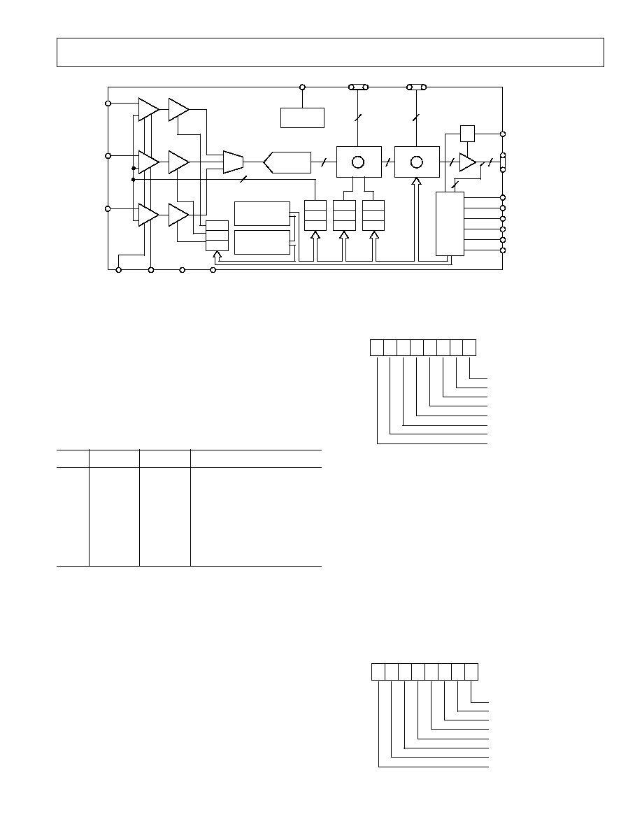
Figure 4. Block Diagram
12-BIT/10-BIT
A/D
PGA
PGA
PGA
GREEN
RED
BLUE
CDS
MUX
BANDGAP
REFERENCE
CONFIGURATION
REGISTER
2
8-10
MPU
PORT
CSB
RDB
WRB
A2
A1
A0
VREF
OFFSET<M:0>
GAIN<N:0>
CDSCLK1
CDSCLK2
VINR
VING
VINB
DOUT<11:0>/MPU<7:0>
CDS
CDS
STRTLN ADCCLK
CONFIGURATION
REGISTER
R
EVEN
G
EVEN
B
EVEN
R
G
B
R
ODD
G
ODD
B
ODD
R
G
B
INPUT OFFSET
REGISTER
12
SUBTRACTOR
DIGITAL
MULTIPLIER
DIGITAL
X
12
12-10/10-8
8
12
12
I/O
OEB
AD9807/AD9805
3
AD9807/AD9805
12
REV. 0
Color Pointer
Both the AD9807 and the AD9805 use Bits 6 and 7 in the
Configuration Register to direct data to the corresponding
internal registers. Table III shows the mapping of Bits 6 and 7
to their corresponding color.
Table III. Color Pointer Map
Bit 7
Bit 6
Color Register
0
0
Red
0
1
Green
1
0
Blue
1
1
RESERVED
Configuration Register 2
Configuration Register 2 controls several functions: color/black
and white selection, CDS enabling, A/D Reference Control
and Input Clamp Mode. Figure 7 shows the AD9807 and
AD9805 Configuration Register 2 format. Setting Bit 0 enables
the three internal CDS blocks of the AD9807/AD9805. Reset-
ting Bit 0 disables the internal CDS blocks, configuring the part
for SHA operation. Setting Bit 1 places the AD9807/AD9805 in
single-channel (black & white) mode. In this mode, only one of
the three input channels is used. The color bits in the configu-
ration register at the time of the last write indicate the particular
channel used. Resetting Bit 1 places the AD9807/AD9805 in
color mode and all three input channels are enabled. Bits 2-4
control the full-scale input span of the A/D. Setting Bit 2 results in
a 4 V p-p input span. Setting Bit 3 results in a 2 V p-p full-scale
input span. Setting Bit 4 results in a full-scale span set by an
external reference connected to the VREF pin of the AD9807/
AD9805 (Full Scale = 2
×
VREF). Resetting Bits 2, 3 or 4
disables that particular mode. Bits 6 and 7 select the desired
clamp mode (see Figure 17). Table IV shows the truth table
for clamp mode functionality. Line clamp mode allows control
of the input switch (S1) via CDSCLK1 only while STRTLN is
reset. Pixel clamp mode allows control of the input switch (S1)
via CDSCLK1 regardless of the state of STRTLN. No clamp
mode disables the input switch (S1) regardless of the selected
mode of CDS operation.
Table IV. Clamp Mode Truth Table
Bit 7
Bit 6
Clamp Mode
0
0
Line Clamp
0
1
Pixel Clamp
1
0
No Clamp
1
1
RESERVED
7
6
5
4
3
2
1
0
CDSEN
BLACK & WHITE
ADC FULL SCALE = 4V
ADC FULL SCALE = 2V
EXTERNAL REFERENCE
SET TO 0
CLAMP MODE SELECT
CLAMP MODE SELECT
Figure 7. AD9807/AD9805 Configuration Register 2 Format
Input Offset Registers
The Input Offset Registers control the amount of analog offset
applied to the analog inputs prior to the PGA portion of the
AD9807/AD9805; there is one Input Offset Register for each
color. Figure 8 shows the Input Offset Register format. The
offset range may be varied between 80 mV and 20 mV. The
data format for the Input Offset Registers is straight binary
coding. An all "zeros" data word corresponds to 80 mV. An
all "ones" data word corresponds to 20 mV. The offset is
variable in 256 steps. The contents of the color pointer in the
Configuration Register at the time an Input Offset Register is
written indicates the color for which that offset setting applies.
7
6
5
4
3
2
1
0
ANALOG OFFSET (LSB)
ANALOG OFFSET
ANALOG OFFSET
ANALOG OFFSET
ANALOG OFFSET
ANALOG OFFSET
ANALOG OFFSET
ANALOG OFFSET (MSB)
Figure 8. Input Offset Registers Format
PGA Gain Registers
Bits 03 of the PGA Gain Registers control the amount of gain
applied to the analog inputs prior to the A/D conversion
portion of the AD9807/AD9805; there is one PGA Gain
Register for each channel. Figure 9 shows the PGA Gain Register
format. The gain range may be varied between 1 and 4. The
data format for the PGA Gain Registers is straight binary
coding. An all "zeros" data word corresponds to an analog
gain of 1. An all "ones" data word corresponds to an analog
gain of 4. The gain is variable in 16 steps (see Figure 16).
The contents of the color pointer in the Configuration
Register at the time a PGA Gain Register is written indicates
the color for which that gain setting applies. Bits 47 of the PGA
Gain Registers are reserved.
7
6
5
4
3
2
1
0
PGA0
PGA1
PGA2
PGA3
RESERVED
RESERVED
RESERVED
RESERVED
Figure 9. PGA Gain Registers Format
Odd, Even Offset Registers
The Odd and Even Offset Registers provide a means of digitally
compensating the odd and even offset error (Register Imbal-
ance) typical of multiplexed CCD imagers; there is one Odd
and one Even Offset Register for each color. Figure 10 shows
the AD9807/AD9805 Odd and Even Offset Register Formats.
The data format for the Odd and Even Offset Registers is twos
complement. The offsets may be varied between positive
AD9807/AD9805
13
REV. 0
127 LSBs and negative 128 LSBs. The offset is variable in
1 LSB increments (see Table V). The contents of the color
pointer in the Configuration Register at the time an Odd or
Even Register is written indicates the color for which that offset
setting applies.
7
6
5
4
3
2
1
0
O/E OFFSET (LSB)
O/E OFFSET
O/E OFFSET
O/E OFFSET
O/E OFFSET
O/E OFFSET
O/E OFFSET
O/E OFFSET (MSB)
Figure 10. Odd and Even Offset Registers Format
Table V. Odd/Even Offset Register Coding
Odd/Even Register Contents
Offset Value
0111 1111
+127 LSB
.
.
.
.
.
.
0000 0001
+1 LSB
0000 0000
0 LSB
1111 1111
1 LSB
.
.
.
.
.
.
1000 0000
128 LSB
DATA BUSES
GAIN<n:0>--The GAIN data bus gives the user access to the
internal digital multiplier. Data from the GAIN bus is latched
into the appropriate internal registers in accordance with the
timing shown in Figure 1. Note that the GAIN data must be
valid on the rising edges of ADCCLK. The contents of the
register become one multiplicand of the digital multiplier; the
output data from the digital subtracter is the other multiplicand.
The AD9807/AD9805 provide a variable word length for the
GAIN data word. Based on the setting in the Configuration
Register, the GAIN data word may be 10, 11 or 12 bits wide
(8, 9 or 10 bits wide for the AD9805). The data format for the
GAIN data bus is straight binary coding. An all "zeros" data
word always corresponds to a gain setting of 1
×
. An all "ones"
data word corresponds to a gain setting dependent on Bits 02
of the Configuration Register. The gain is variable in 1024,
2048, or 4096 (256, 512 or 1024 for the AD9805) increments
depending on the width of GAIN data word.
OFFSET<m:0>
The OFFSET data bus gives the user access to the internal
digital subtracter. Data from the OFFSET bus is latched into
the appropriate internal registers in accordance with the timing
shown in Figure 1. Note that the OFFSET data must be valid
on the rising edges of ADCCLK. The contents of the register
become the subtrahend; the output data from the A/D converter
(after odd/even correction) is the other input. The AD9807/
AD9805 provide a variable word length for the OFFSET data
word. Based on the setting in the Configuration Register, the
OFFSET data word may be 8, 9 or 10 bits wide. The data
format for the OFFSET data bus is straight binary coding. An
all "zeros" data word corresponds to an offset value of 0 LSBs.
An all "ones" data word subtracts an offset value of 256, 512 or
1024 LSBs, depending on the width of OFFSET data word.
The offset is variable in 256, 512 or 1024 increments.
DOUT<n:0>--The DOUT data bus is bidirectional. CMOS
compatible digital data is available as an output on the DOUT
bus. Data is coded in straight binary format. When CSB and
either WRB or RDB are applied to the AD9807/AD9805, the
DOUT data bus becomes an input/output port for the register
data, shown as MPU<7:0>. The timing and latency for the
DOUT data bus are given in Figures 11 through 15.
FUNCTIONAL OVERVIEW
It is possible to operate the AD9807/AD9805 in one of five
modes: 3-Channel Operation with CDS, 3-Channel SHA
Operation, 1-Channel Operation with CDS, 1-Channel SHA
Operation and 2-Channel Bayer Mode. A description of each of
the five modes follows.
3-Channel Operation with CDS
This mode of the AD9807/AD9805 enables simultaneous
sampling of a triple output CCD. The CCD waveforms are ac
coupled to the VINR, VING and VINB pins of the AD9807/
AD9805 where they are automatically biased at an appropriate
voltage level using the on-chip clamp; the inputs may alterna-
tively be dc coupled if they have already been appropriately level
shifted. The internal CDSs take two samples of the incoming
pixel data: the first samples (CDSCLK1) are taken during the
reset time while the second samples (CDSCLK2) are taken
during the video, or data, portion of the input pixels. The offsets
of the three input channels are modified by the values stored in
the input offset registers. The voltage differences of the reset
levels and video levels are inverted and amplified by the PGAs;
the settings in the corresponding PGA Gain Registers determine
the gains of the PGAs. These outputs from the PGAs are then
routed through a high speed multiplexer to a 12-bit A/D
converter (10-bit for AD9805) for digitization; the multiplexer
cycles between the red, green and then blue channels. After
digitization, the data is modified by the amount indicated in the
Odd and Even Offset Registers. A digital subtracter allows
additional pixel rate offset modification of each color based on
the values written to the OFFSET data bus. Finally, a digital
multiplier allows pixel rate gain modification of each color based
on the values written to the GAIN data bus. Latency for the red,
green and blue channels is 6 ADCCLK cycles (9 cycles for the
gain and offset bus; see Figure 12).
The STRTLN signal indicates the first red, green and blue
pixels in a scan line, and the red channel is always the first pixel
digitized. The state of STRTLN is evaluated on the rising
edges of ADCCLK. When STRTLN is low, the internal
circuitry is reset on the next rising edge of ADCCLK; the
multiplexer is switched to the red channel and the odd/even
circuitry is configured to expect even pixels. After STRTLN
goes high, the first set of pixels is assumed to be even. Consecu-
tive sets of pixels (red, green and blue) are assumed to alternate
between odd and even pixel sets.

AD9807/AD9805
14
REV. 0
3-Channel SHA Operation
This mode of the AD9807/AD9805 enables 3-channel simulta-
neous sampling; it differs from the CDS sampling mode in that
the CDS functions are replaced with sample-and-hold amplifiers
(SHAs). CDSCLK1 becomes the sample-and-hold clock;
CDSCLK2 is tied to ground. The input is sampled on the
falling edge of CDSCLK1. The input signals must be either dc
coupled and level shifted, or dc restored prior to driving the
VINR, VING, and VINB pins of the AD9807/AD9805 (clamp
mode must be disabled). The input signal in this mode is
ground-referenced. The offsets of the three input channels are
modified by the values stored in the input offset registers. The
part does not invert the input signals prior to amplification by
the PGAs; the settings in the corresponding PGA Gain Registers
determine the gains of the PGAs. These outputs from the
PGAs are then routed through a high speed multiplexer to a
12-bit A/D converter (10-bit for AD9805) for digitization; the
multiplexer cycles between the red, green and then blue
channels. After digitization, the data is modified by the amount
indicated in the Odd and Even Offset Registers. A digital
subtracter allows additional pixel rate offset modification of
each color based on the values written to the OFFSET data bus.
Finally, a digital multiplier allows pixel rate gain modification
of each color based on the values written to the GAIN data bus.
Latency for the red, green and blue channels is 6 ADCCLK
cycles (9 cycles for the gain and offset bus; see Figure 13).
The STRTLN signal indicates the first red, green and blue
pixels in a scan line and the red channel is always the first pixel
digitized. The state of STRTLN is evaluated on the rising
edges of ADCCLK. When STRTLN is low, the internal
circuitry is reset on the next rising edge of ADCCLK; the
multiplexer is switched to the red channel and the odd/even
circuitry is configured to expect even pixels. After STRTLN
goes high, the first set of pixels is assumed to be even. Consecu-
tive sets of pixels (red, green and blue) are assumed to alternate
between odd and even pixel sets.
1-Channel Operation with CDS
This mode of the AD9807/AD9805 enables single-channel, or
monochrome, sampling. The CCD waveform is ac coupled to
either the VINR, VING, and VINB pin of the AD9807/AD9805
where it is biased at an appropriate voltage level using the on-
chip clamp; the input may alternatively be dc coupled if it has
already been appropriately level shifted. Bits 6 and 7 in the
Configuration Register select the desired input. The internal
CDS takes two samples of the incoming pixel data: the first
sample (CDSCLK1) is taken during the reset time while the
second sample (CDSCLK2) is taken during the video, or data,
portion of the input pixel. The offset of the input signal is
modified by the value stored in the input offset register. The
voltage difference of the reset level and video level is inverted and
amplified by the PGA; the setting in the corresponding PGA
Gain Register determines the gain of the PGA. The output
from the PGA is then routed through a high-speed multiplexer
to a 12-bit A/D converter (10-bit for AD9805) for digitization;
the multiplexer does not cycle in this mode. After digitization,
the data is modified by the amount indicated in the Odd and
Even Offset Registers. A digital subtracter allows additional
pixel rate offset modification of the signal based on the values
written to the OFFSET data bus. Finally, a digital multiplier
allows pixel rate gain modification of the signal based on the
values written to the GAIN data bus. Latency is 6 ADCCLK
cycles (7 cycles for the gain and offset bus; see Figure 14).
The state of STRTLN is evaluated on the rising edges of
ADCCLK. When STRTLN is low, the internal circuitry is
reset on the next rising edge of ADCCLK; the odd/even
circuitry is configured to expect an even pixel. After STRTLN
goes high, the first pixel is assumed to be even. Consecutive
pixels (red, green or blue) are assumed to alternate between odd
and even. The blue and green channels are recommended for
single channel operation to achieve the maximum sampling rate;
if using red, invert ADCCLK as shown in Figure 1d.
1-Channel SHA Operation
This mode of the AD9807/AD9805 enables single-channel, or
monochrome sampling; it differs from the CDS monochrome
sampling mode in that the CDS function is replaced with a
sample-and-hold amplifier (SHA). CDSCLK1 becomes the
sample-and-hold clock; CDSCLK2 is tied to ground. The
input is sampled on the falling edge of CDSCLK1. The input
waveform would typically be either dc coupled and level shifted,
or dc restored prior to driving either the VINR, VING and
VINB pins of the AD9807/AD9805 (clamp mode must be
disabled).
Bits 6 and 7 in the Configuration Register select the desired
input. The input signal in this mode is ground referenced. The
input signal is not inverted prior to amplification by the PGA;
the setting in the corresponding PGA Gain Register determines
the gain of the PGA. The offset of the input signal is modified
by the value stored in the input offset register. This signal is
then routed through a high speed multiplexer to a 12-bit A/D
converter (10-bit for AD9805) for digitization; the multiplexer
does not cycle in this mode. After digitization, the data is
modified by the amount indicated in the Odd and Even Offset
Registers. A digital subtracter allows additional pixel rate offset
modification of the signal based on the values written to the
OFFSET data bus. Finally, a digital multiplier allows pixel rate
gain modification of the signal based on the values written to the
GAIN data bus. Latency is 6 ADCCLK cycles (7 cycles for
gain and offset; see Figure 15).
The state of STRTLN is evaluated on the rising edges of
ADCCLK. When STRTLN is low, the internal circuitry is
reset on the next rising edge of ADCCLK; the odd/even
circuitry is configured to expect an even pixel. After STRTLN
goes high, the first pixel is assumed to be even. Consecutive
pixels (red, green or blue) are assumed to alternate between odd
and even. The blue and green channels are recommended for
single channel operation to achieve the maximum sampling rate;
if using red, invert ADCCLK as shown in Figure 1f.
2-Channel Bayer Mode Operation with CDS
This mode of the AD9807/AD9805 enables Bayer Mode. The
CCD waveform is ac coupled to both the VING and VINB pins
of the AD9807/AD9805 where it is biased at an appropriate
voltage level using the on-chip clamp; the input may alterna-
tively be dc coupled if it has already been appropriately level
shifted. The internal CDS takes two samples of the incoming
pixel data: the first sample (CDSCLK1) is taken during the
reset time while the second sample (CDSCLK2) is taken during
the video, or data, portion of the input pixel. The offset of the
input signal is modified by the value stored in the input offset
register. The voltage difference of the reset level and video level
AD9807/AD9805
15
REV. 0
R (n2)
G (n2)
B (n2)
R (n1)
G (n1)
B (n1)
R (n)
PIXEL n
PIXEL n+1
PIXEL n+2
R, G, B
R, G, B
R, G, B
R
G
B
R
G
B
R
G
B
RIN, GIN, BIN
CDSCLK1
CDSCLK2
ADCCLK
DATA<11:0>
G (n+1)
B (n+1)
R (n+2)
G (n+2)
B (n+2)
R (n+3)
GAIN<n:0>
GAIN<m:0>
R (n)
G (n)
B (n)
R (n+1)
Figure 12. DOUT Latency, 3-Channel CDS Mode
t
OD
t
HZ
t
EDV
ADCCLK
DATA<11:0>
OEB
Figure 11. Digital Output Timing
is inverted and amplified by the PGA; the setting in the corre-
sponding PGA Gain Register determines the gain of the PGA.
The output from the PGA is then routed through a high speed
multiplexer to a 12-bit A/D converter (10-bit for AD9805) for
digitization; the multiplexer does cycle in this mode. After
digitization, the data is modified by the amount indicated in
the Even Offset Registers. A digital subtracter allows additional
pixel rate offset modification of the signal based on the values
written to the OFFSET data bus. Finally, a digital multiplier
allows pixel rate gain modification of the signal based on the
values written to the GAIN data bus. Latency is 6 ADCCLK
cycles (7 cycles for the gain and offset bus; see Figure 14).
The state of STRTLN is evaluated on the rising edges of
ADCCLK. When STRTLN is low, the internal circuitry is
reset on the next rising edge of ADCCLK; the odd/even
circuitry is configured to expect even pixels.
This feature has been included to accommodate the use of the
part with an area CCD (Bayer Mode). The mode is initiated by
writing a one to the LSB of the register at Address 7 (see Figure
21). The write to enable the mode should be performed when
the STRTLN input is inactive (low) and the ADCCLK is running.
The first pixel after an active edge on STRTLN will be a green
pixel. All pixels in Bayer Mode are even and use the even offset
registers. The line will continue alternating GRGRGR pixels
until STRTLN goes inactive. The next line will be BGBGBG
pixels (the first pixel after the active STRTLN edge being blue).
Line type will then alternate between GRGRGR and BGBGBG
type. To reset the next line to GRGRGR type at the start of the
next frame/image, rewrite the Bayer mode enable bit to a one
during the inactive STRTLN period. All red and blue pixels
pass through the blue channel of the part and use the blue PGA
and offset registers. To use a different offset/PGA gain value the
register must be written to between lines. Green pixels on either
line type pass through the green channel.
AD9807/AD9805
16
REV. 0
PIXEL n
PIXEL n+1
PIXEL n+2
R, G, B
R, G, B
R, G, B
R
G
B
R
G
B
R
G
B
R (n2)
G (n2)
B (n2)
R (n1)
G (n1)
B (n1)
RIN, GIN, BIN
CDSCLK1
ADCCLK
DATA<11:0>
R (n)
G (n+1)
B (n+1)
R (n+2)
G (n+2)
B (n+2)
R (n+3)
GAIN<n:0>
GAIN<m:0>
R (n)
G (n)
B (n)
R (n+1)
Figure 13. DOUT Latency, 3-Channel SHA Mode
RIN, GIN, BIN
CDSCLK2
ADCCLK
DATA<11:0>
PIXEL n
PIXEL n+1
PIXEL n+2
CDSCLK1
D (n7)
D (n6)
D (n5)
D (n8)
GAIN<n:0>
OFFSET<m:0>
D (n4)
G (n+1)
G (n+2)
G (n+3)
G (n)
Figure 14. DOUT Latency, 1-Channel CDS Mode
G (n+1)
G (n+2)
G (n+3)
GAIN<n:0>
OFFSET<m:0>
PIXEL n
PIXEL n+1
PIXEL n+2
RIN, GIN, BIN
CDSCLK1
ADCCLK
D (n7)
D (n6)
D (n5)
D (n4)
DATA<11:0>
G (n)
Figure 15. DOUT Latency, 1-Channel SHA Mode
AD9807/AD9805
17
REV. 0
Choosing the Input Coupling Capacitors
Because of the dc offset present at the output of CCDs, it is likely
that these outputs will require some form of dc restoration to be
compatible with the input requirements of the AD9807/AD9805.
To simplify input level shifting, a dc blocking capacitor may be
used in conjunction with the internal biasing circuits of the
AD9807/AD9805 to accomplish the necessary dc restoration.
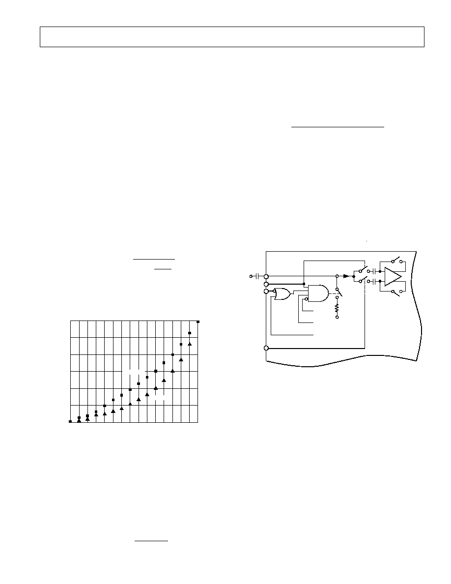
Figure 17 shows the equivalent analog input for the VINR,
VING and VINB inputs.
I
BIAS
S1
V
BIAS
AD9807/AD9805
C
V
IN
CDSCLK1
STRTLN
CONFIG
REG 2<7>
CONFIG
REG 2<6>
CONFIG
REG 2<0>
CDSCLK2
CDS
5k
4pF
4pF
Figure 17. Equivalent Analog Inputs (VINR, VING, and
VINB)
Enabling CDS functionality and Line Clamp Mode with Bits 0,
6 and 7 in Configuration Register 2 allows switch S1 to turn on
when STRTLN is low and CDSCLK1 goes high. This connects
a 5 k
biasing resistor to the inputs. This arrangement acts to
bias the average level of the input signal at voltage, V
BIAS
. The
voltage, V
BIAS
, changes depending on the selected PGA gain set-
ting. Specifically, for gain settings from 0 to 5, V
BIAS
equals 4 V;
for gain settings from 10 to 15, V
BIAS
equals 3 V. For gain set-
tings between 5 and 10, V
BIAS
decreases linearly from 4 V to 3 V.
The size of the coupling capacitor is dependent on several
factors including signal swing, allowable droop, and acquisition
time. The following procedure shows how to determine the
recommended range of capacitors.
Calculating C
MAX
The maximum capacitor value is largely dependent on the
degree of accuracy and how quickly the input signal must be
level-shifted into the valid input range of the degree of accuracy.
Other factors affecting the speed of the capacitor charging or
Calculating Overall Gain
The overall gain for the AD9807/AD9805 can accommodate a
wide range of input voltage spans. The total gain is a composite
of analog gain (from the PGAs), digital gain (from the digital
multiplier) and the input span setting for the A/D (2 V or 4 V). To
determine the overall gain setting for the AD9807/AD9805, always
multiply the PGA gain setting by the digital gain setting. In
addition, the 2 V/4 V reference option can effectively provide
analog gain for input signals less than 2 V p-p.
Overall Gain = Analog Gain
×
Digital Gain
For example, with the PGA gain equal to 1 (gain setting equals
all "zeros") and the digital multiplier equal to 1, the minimum
gain equals 1. With these settings, input signals can be as large
as 2 V or 4 V depending on the reference setting. Alternatively,
with the PGA gain equal to 4 (gain setting equals all "ones")
and the digital multiplier equal to 8, the maximum gain equals
32. With the A/D reference span set to 2 V, an input signal span
as small as 62.5 mV p-p will produce a digital output spanning
from all "zeros" to all "ones." For ranges between 62.5 mV and
4 V, see the Digital Gain and Analog Gain sections of the data
sheet.
Analog Gain
The transfer function of the PGA is:
Analog Input
=
4
1
+
3
×
15
-
x
15
where x is the decimal representation of the settings in the PGA
gain register. Figure 16 shows the graph of this transfer
function on both a linear and logarithmic scale. The transfer
function is approximately linear in dB.
12
6
0
10
8
4
2
GAIN dB
4.0
2.5
1.0
3.5
3.0
2.0
1.5
GAIN
PGA GAIN SETTING
0
13
1
2
3
4
5
6
7
8
9
10 11 12
14 15
GAIN
GAIN (dB)
Figure 16. PGA Transfer Function
Digital Gain
The digital multiplier section of the AD9807/AD9805 allows the
user to apply gain in addition to that afforded by the analog
PGA. The minimum gain of the digital multiplier is always 1.
The user sets the maximum gain of the digital multiplier to be 8,
4, or 2 with Bits 02 in the Configuration Register. (The max
gain is the same for all three channels.) The digital gain
applied to the output from the digital subtracter is calculated
using the equation:
Digital Gain
=
1
+
Gain
<
n:0
>
Y
×
X
where GAIN<n:0> is the decimal representation of the GAIN
bus data bits, Y = 4096 for the AD9807, Y = 1024 for the
AD9805, and X equals 1, 3 or 7 depending on Bits 02 in the
Configuration Register.
Overall Transfer Function
The overall transfer function for the AD9807 can be calculated
as follows:
ADC
OUT
=
V
IN
±
InputOffset
(
)
×
PGA Gain
[
]
2
×
V
REF
×
4096
D
OUT
= [ADC
OUT
+ Offset Register Offset Bus][Digital Gain]

AD9807/AD9805
18
REV. 0
discharging include the amount of time that input switch S1 is
turned on, the input impedance of the AD9807/AD9805 and
the output impedance of the circuit driving the coupling
capacitor. The impedance of the drive circuit, R
OUT
, the input
impedance of the AD9807/AD9805, R
IN
, and the desired
charging time, t
ACQ
, are all known quantities. Note that t
ACQ
may not necessarily occur over a continuous period of time; it may
actually be an accumulation of discrete charging periods. This
is typical where CDSCLK1 is asserted only during the reset
levels of the pixels. In this case, the quantity, m
×
T, may be
substituted for t
ACQ
, where m is the number of periods
CDSCLK1 is asserted and T is the period of the assertion.
Given these quantities, the maximum value for the input
coupling capacitor is computed from the equation:
C
MAX
t
ACQ
R
IN
+
R
OUT
/ ln
V
C
V
E
where V
C
is the required voltage change across the coupling
capacitor and V
E
is the maximum tolerable error voltage. V
C
is
calculated by taking the difference between the CCD's reset
level and the internal bias level of the AD9807/AD9805. V
E
is
the level of accuracy to which the input capacitor must be charged
and is system dependent. Usually the allowable droop of the
capacitor voltage is taken into account. This is discussed below.
For example, if the CCD output can droop up to 1 volt without
affecting the accuracy of the CDS, then clamping to within
about one tenth of the allowable droop (100 mV) should be
sufficient in most cases.
Calculating C
MIN
Determining C
MIN
is a function of the amount of allowable
voltage droop. It is important that the signals at the inputs of
the AD9807/AD9805 remain within the supply voltage limits so
the CDSs are able to accurately digitize the difference between
the reset level and the video level. Assuming the input voltages
are initially biased at the correct levels, the input bias current of
the AD9807/AD9805 inputs will discharge the input coupling
capacitors resulting in voltage droop. After taking into account
any droop, the peaks of the input signal must remain within the
required voltage limits of AD9807/AD9805 inputs.
Specifically, C
MIN
is a function of the maximum allowable
droop, dV, in one scan line, the number of pixels across one scan
line, n, the period of one pixel, t, and the input bias current of
the AD9807/AD9805, I
BIAS
. C
MIN
is calculated from the equation:
C
MIN
=
I
BIAS
dV
×
n
×
t
Some examples are given below showing the typical range of
capacitor values.
Example 1
A 5000 pixel CCD running at a 2 MHz (t = 500 ns) has a reset
level of 4.5 volts and an output voltage of 1.8 volts. The number
of optical black pixels available at the start of a line is 18. Using
the AD9807/AD9805 with an input span of 4 volts and a PGA
gain of 2 gives a V
BIAS
of 3 volts. If the input signal is clamped
to 3 volts during the optical black pixels, the required voltage
change on the input capacitor, V
C
, equals (4.5 3) or 1.5 volts
and the maximum droop allowable during one line, dV, will be
(3 1.8) or 1.2 volts before the signal droops below 0 volts.
With dV = 1.2 volts, a clamp accuracy of 100 mV should be
sufficient (V
E
=100 mV), but this value can be adjusted. The
amount of time available to charge up the input capacitor,
T
ACQ
, will equal the period of CDSCLK1 (when the clamp
switch is closed) times the number of optical black pixels. With
a pixel rate of 2 MHz, CDSCLK1 would typically be around
100 ns wide, giving T
ACQ
=1800 ns or
1.8
µ
s. The input impedance of the AD9807 is 5K, and the
input bias current is 10 nA. Assume the source impedance
driving the AD9807 is low (R
OUT
= 0).
C
MAX
= (1.8
µ
s/5K)
×
(1/ln (1.5/0.1)) = 133 pF
C
MIN
= (10 nA/1.2)
×
5000
×
500 ns = 21 pF
Note that a capacitor larger than 133 pF would still work, it
would just take several lines to charge the input capacitor up
to the full V
C
level. Another option to lengthen T
ACQ
is by
clocking the CCD and CDSCLK1 while the transport motor
moves the scanner carriage. This would extend T
ACQ
to
several hundred
µ
s or more, meaning that only very fine
adjustment would be needed during the limited number of
optical black pixels.
Example 2
A 7926 pixel CCD running at 2 MHz has a reset level of 6 volts,
an output voltage of 2.9 volts and 80 optical black pixels. Using
the AD9807 with an input span of 4 volts and a PGA gain of
1.25, V
BIAS
= 4 volts. The maximum required voltage change
on the capacitor, V
C
, is 2 volts and the maximum amount of
droop dV for one line is 1.1 volts. T
ACQ
will be 80
×
100 ns or 8
µ
s, and V
E
= 100 mV should be sufficient. Again, R
IN
= 5K,
R
OUT
= 0, and I
BIAS
= 10 nA.
C
MAX
= (8
µ
s/5K)
×
(1/ln (2/0.1))
534 pF
C
MIN
= (10 nA/1.1)
×
(7926)
×
(500 ns) = 36 pF
Again, a larger capacitor may be used if several lines are allowed
for to initially charge up the cap, or if the CCD and CDSCLK1
are clocked during the moving of the scanner carriage.
Generating 3-Channel Timing from a 16 Master Clock
Generating the required signals for CDSCLK1, CDSCLK2 and
ADCCLK is easily accomplished with a master clock running
16
×
the desired per channel pixel rate (i.e., 2 MSPS pixel rate
requires 32 MHz master clock). The timing diagram shown
in Figure 18 meets all the minimum and maximum timing
specifications. Note that a 16
×
master clock using only rising
edges was chosen instead of using both edges of an 8
×
rate
clock to ensure immunity to duty cycle variations.
MASTER
(32MHz)
CDSCLK1
CDSCLK2
ADCCLK
1
2
3
4
5
6
7
8
9
10
11
12
13
14
15
16
500ns
Figure 18. Timing Scheme Using 16
×
Master Clock
AD9807/AD9805
19
REV. 0
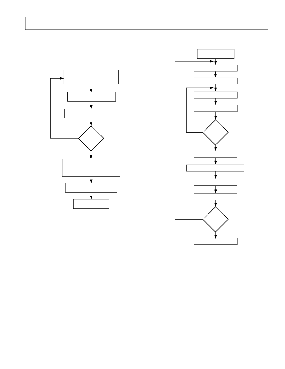
To calibrate the AD9807/AD9805 for a particular scan, use the
following sequence.
SET DIGITAL GAIN RANGE
YES
NO
SET PGA GAIN(S)
(INPUT OFFSET = 0mV)
SCAN DARK LINE
COMPUTE PIXEL OFFSETS
SET INPUT OFFSET
SET ODD/EVEN OFFSET
SET GAIN/OFFSET BUS SIZE
SET EXTERNAL PIXEL OFFSET VECTORS
SCAN WHITE LINE
NO
ADJUST
PGA GAIN(S)
?
COMPUTE PIXEL GAINS
SET
ANOTHER
COLOR
?
YES
Figure 20. Calibration
Power-On Initialization and Calibration Sequence
When the AD9807/AD9805 is powered on, the following
sequence should be used to initialize the part to a known state.
The digital gain and offset buses are disabled until the calibra-
tion sequence. The Bayer mode register must be written to and
set to zero if this mode is not going to be used.
WRITE TO CONFIGURATION REGISTER
SET DIGITAL GAIN RANGE TO 000
SET GAIN/OFFSET BUS SIZE TO 000
SET COLOR POINTER
OPTIONAL READBACK
FROM REGISTERS
WRITE TO PGA GAIN REGISTER
SET TO GAIN OF ONE (0000)
WRITE TO INPUT OFFSET REGISTER
SET TO 0mV (11001100)
WRITE TO CONFIGURATION 2 REGISTER
SET CDS OR SHA OPERATION
SET 3-CHANNEL OR 1-CHANNEL MODE
SET ADC FULL-SCALE RANGE
SET CLAMP MODE
WRITE TO BAYER MODE REGISTER
SET MODE ON OR OFF
YES
NO
CHANGE
POINTER
SET
ANOTHER
COLOR
?
Figure 19. Initialization
AD9807/AD9805
20
REV. 0
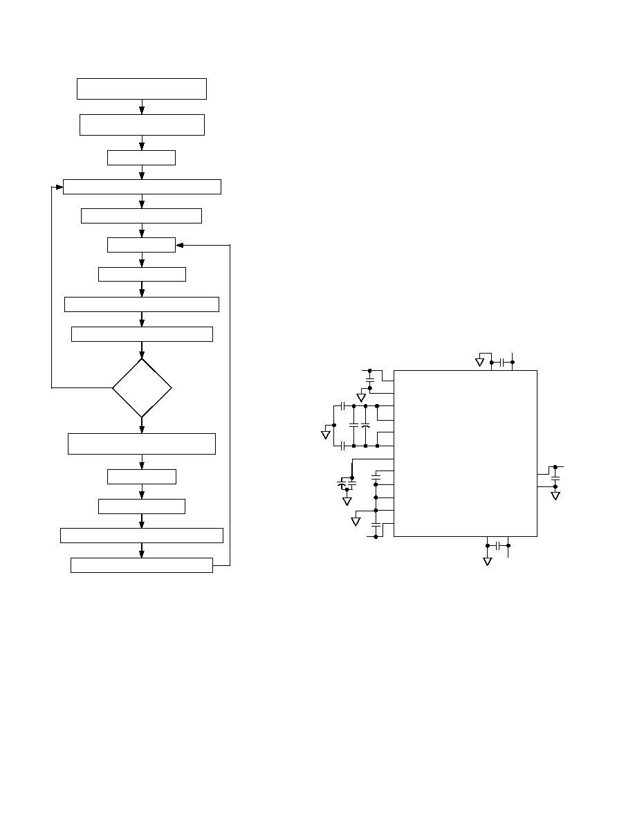
NO
BRING STRTLN HIGH
THE FIRST PIXEL IS GREEN
THE SECOND PIXEL IS RED, ALTERNATING GRGR...
BRING STRTLN LOW AT THE END OF THE LINE
NEXT LINE
GRGR AGAIN
(NEW FRAME)
?
YES
APPLY AT LEAST ONE ADCCLK CYCLE
WRITE A "1" TO THE LSB OF THE BAYER REGISTER
BRING STRTLN LOW
SET PGA AND INPUT OFFSET FOR RED
PIXELS USING THE BLUE REGISTERS
SET PGA AND INPUT OFFSET FOR GREEN
PIXELS USING THE GREEN REGISTERS
CHANGE THE PGA AND INPUT OFFSET OF BLUE
REGISTERS FOR BLUE PIXELS
BRING STRTLN HIGH
THE FIRST PIXEL IS BLUE
THE SECOND PIXEL IS GREEN, ALTERNATING BGBG...
BRING STRTLN LOW AT THE END OF THE LINE
CHANGE GAIN
AND OFFSET
FOR RED PIXELS
WITH BLUE
REGISTERS
Figure 21. Bayer Mode Operation
Grounding and Decoupling
Figure 22 shows the recommended decoupling capacitors and
ground connections for the AD9807/AD9805. Notice that all of
the power and ground connections are common for the analog
and digital portions of the chip. This would be the best way to
connect the device on a board containing a large number of
digital components. By treating the AD9807/AD9805 as an
analog component, the on-board digital circuitry is considered
"quiet digital" and the digital supply pins are connected to the
clean analog supply and analog ground plane. For this tech-
nique to work well, it is important that the digital supply pins be
well decoupled to the analog ground plane and that the digital
outputs of the AD9807/AD9805 are buffered to minimize the
digital drive current. The buffers would be referred to the digital
supply and ground. This scheme is preferable to tying the digital
portion of the AD9807/AD9805 to a noisy digital ground and
power plane, capacitively coupling noise to the analog circuitry
within the device. The AD9807/AD9805 evaluation boards use
this grounding method, shown in Figures 26 and 27. If a
minimum amount of digital circuitry exists on the board, it is
possible that the power and ground connections of the AD9807
can be separated; be sure to maintain a single point connection
between the two ground planes at the AD9807/AD9805.
+5
0.1µF
0.1µF
0.1µF
10µF
+
0.1µF
+
10µF
0.1µF
0.1µF
0.1µF
+5
52
+5
0.1µF
0.1µF
+5
28
+5
0.1µF
DVSS
DVDD
29
41
40
51
1
AD9807/AD9805
(PINS OMITTED FOR CLARITY)
AVDD
AVSS
CAPT
CAPT
CAPB
CAPB
REF
CML
AVSS
AVSS
AVSS
AVDD
DVSS
DRVDD
DRVSS
2
3
4
5
6
7
8
10
12
14
15
DVSS
DVDD
Figure 22.
AD9807/AD9805
21
REV. 0
CIS Application
Unlike many other integrated circuit CCD signal processors, the
AD9807/AD9805 can easily be implemented in imaging systems
that do not use a CCD. By disabling the input clamp and the
CDS blocks, any dc coupled signal within the input limits of the
part can be digitized. Figure 23 shows a typical block diagram of
the AD9807 used with a color CIS module, in this case Dyna
Image Corporation's DL100*. The three color output signals
are dc coupled into the AD9807. The Dyna CIS module's
output levels are around 70 mV to 500 mV dark to bright, well
within the input range of the AD9807. The AD9807 is config-
ured for 3-channel SHA operation through the MPU registers.
Timing used with the Dyna DL100 is shown in Figure 24; the
CIS output levels are sampled on the falling edge of CDSCLK1.
The digital ASIC shown can be implemented in a variety of
ways: it could include the MPU interface and timing generator,
as well as memory for the output data and pixel gain and offset
correction vectors.
RED
GREEN
BLUE
CIS
CLOCKS
VINR
VING
VINB
STRTLN,
CDSCLK1,
ADCCLK
OFFSET<7:0>
GAIN<11:0>
TIMING
GENERATOR
DIGITAL
ASIC
MPU
INTERFACE
PIXEL
OFFSET
CORRECTION
PIXEL
GAIN
CORRECTION
DOUT<11:0>
MPU<7:0>
A2, A1, A0
OEB, WRB
RDB, CSB
CIS
12
7
8
12
8
3
OUTPUT
DATA
AD9807
Figure 23. CIS Application Diagram (Power, Ground, and
Decoupling Omitted)
CIS START PULSE
CIS CLOCK
CIS OUTPUT
STRTLN
ADCCLK
CDSCLK1
Figure 24. CIS Application Timing Signals
EVALUATION BOARDS
The AD9807 and AD9805 evaluation boards are designed to
provide an easy interface to a standard PC, simplifying the task
of evaluating the performance of the AD9807/AD9805 with an
existing imaging system. The system level block diagram shown
in Figure 25 illustrates the basic evaluation setup for the
AD9807 (the AD9805 is the same). The user needs to supply
the analog input signals (such as outputs from a CCD), the
AD9807/AD9805's clock signals, a power supply and a printer
cable to connect the evaluation board to the PC's parallel port.
Software is included to allow the user to easily accomplish three
major tasks: first, configure the AD9807/AD9805 in one of several
operating modes (1 Channel, 3 Channel, CDS or SHA mode,
etc.), second, acquire output data from the part and third, down-
load pixel gain and offset correction data to the evaluation board
and enable pixel rate shading and offset correction.
Figures 26 and 27 show the signal routing and decoupling for
the AD9807 evaluation board.
The evaluation boards are designated with the part numbers
AD9807-EB and AD9805-EB.
*All trademarks are properties of their respective holders.
VINR
VING
VINB
CLOCKS
GAIN
OFFSET
DOUT
MPU I/O
MPU CONTROL
AD9807
RED
GREEN
BLUE
STRTLN
CDSCLK1
CDSCLK2
ADCCLK
4
12
8
12
8
7
FIFO
BUFFERS,
LATCHES,
AND
CONTROL
LOGIC
8
PRINTER
CABLE
PC
PARALLEL
PORT
AD9807 EVALUATION BOARD
+5V VOLT
POWER
SUPPLY
ANALOG INPUTS
CLOCK INPUTS
Figure 25. Evaluation System Block Diagram
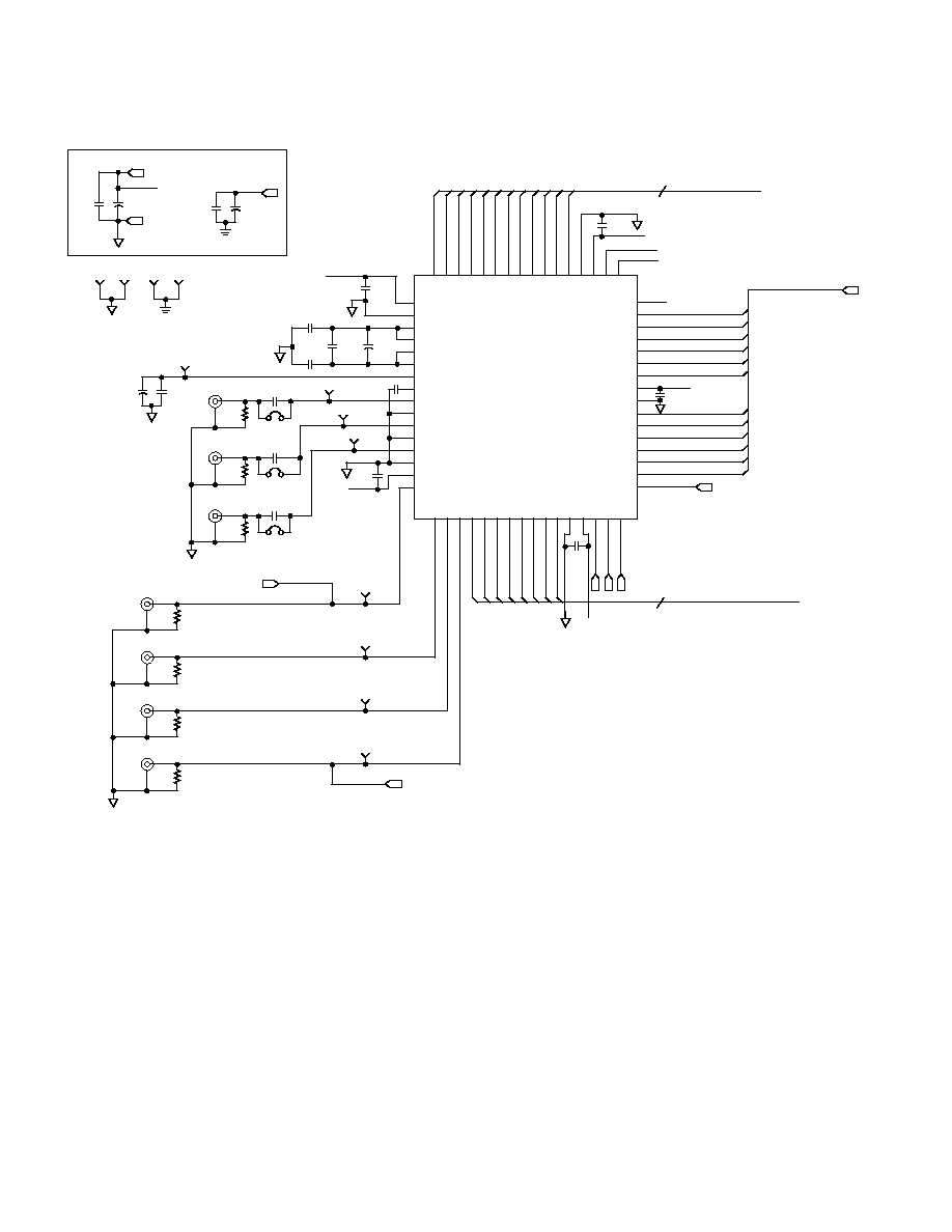
AD9807/AD9805
22
REV. 0
AVDD
AVSS
CAPT
CAPT
CAPB
CAPB
REF
CML
VINR
AVSS
VING
AVSS
VINB
AVSS
AVDD
ST_LIN
A0
D(11)
D(10)
D(9)
D(8)
D(7)
D(6)
DRVDD
DRVSS
D(5)
D(4)
D(3)
D(2)
D(1)
D(0)
OEB
CDS1
CDS2
ADCLK
OFF(7)
OFF(6)
OFF(5)
OFF(4)
OFF(3)
OFF(2)
OFF(1)
OFF(0)
DVSS
DVDD
CSB
RDB
WRB
G(11)
G(10)
G(9)
G(8)
G(7)
G(6)
G(5)
G(4)
G(3)
G(2)
G(1)
G(0)
DVSS
DVDD
A2
A1
AD9807
DVDD
C13
0.1µ
AD9807 DATABUS
D11
D10
D9
D8
D7
D6
D5
D4
D3
D2
D1
D0
OEB
C15
0.1µF
DVDD
A2
A1
GAIN
12
C7
0.1µF
C6
10µF
C12
0.1µF
AVDD
C8
0.1µF
C10
0.1µF
C4
0.1µF
AVDD
TP7
TP6
TP5
C1
0.01µF
C2
0.01µF
C3
0.01µF
JP3
JP2
JP1
R7
50
B5
R6
50
B6
R5
50
B7
TP5
C27
0.1µF
+
C28
10µF
+
TP14
TP13
TP16
TP15
C25
10µF
C26
0.1µF
+
+5VD
C18
10µF
C21
0.1µF
+
DVDD
AVSS
AVDD
TP9
STARTLINE
R4
50
B1
PL
PL
PL
PL
STARTLINE
TP10
R3
50
B2
PL
CDS1
TP11
R2
50
B3
PL
CDS2
TP12
R1
50
B4
PL
ADC
ADCCLK
DVDD
8
OFFSET
1
2
3
4
5
6
7
8
9
10
11
12
13
14
15
16
48
47
46
45
44
43
42
41
40
39
38
37
36
35
34
33
49
50
51
52
53
54
55
56
57
58
59
60
61
62
63
64
32
31
30
29
28
27
26
25
24
23
22
21
20
19
18
17
C11
0.1µF
C14
0.1µF
Figure 26. AD9807 Evaluation Board (Digital Circuitry Omitted)
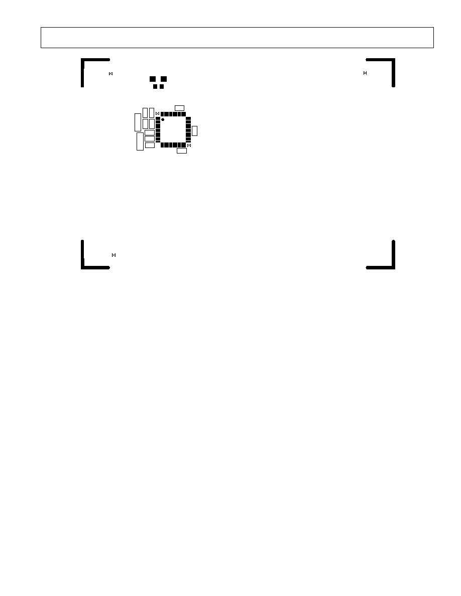
AD9807/AD9805
23
REV. 0
+C6
+C28
C27
C4
C11
C8
C12
C10
C7
C15
C14
C13
Figure 27. Suggested Capacitor Placement for Single-Side Component Layout
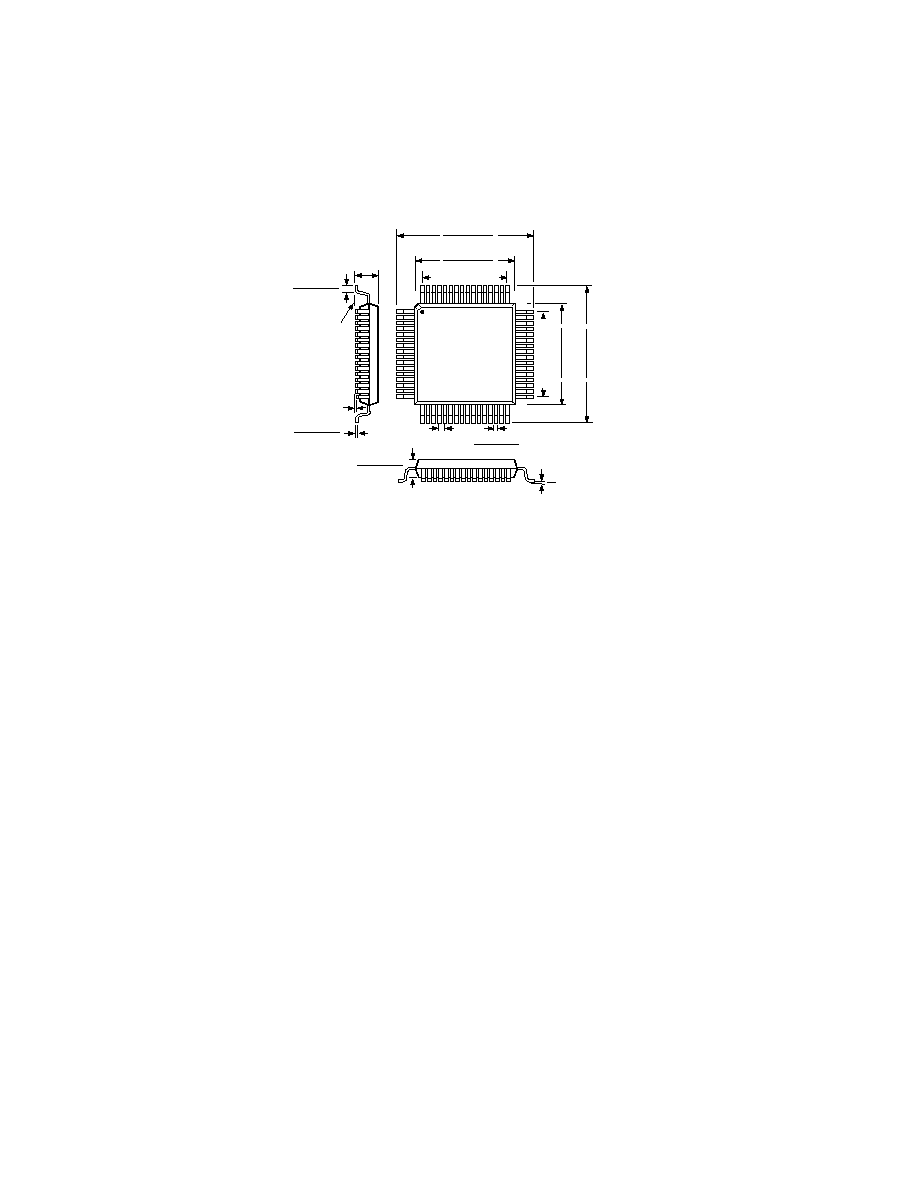
AD9807/AD9805
24
REV. 0
C2196121/97
PRINTED IN U.S.A.
64-Terminal PQFP
(S-64)
7
°
0
°
0.083 (2.10)
0.077 (1.95)
SEATING
PLANE
0.093 (2.35)
MAX
0.041 (1.03)
0.029 (0.73)
STANDOFF
0.010 (0.25)
0.009 (0.23)
0.005 (0.13)
PIN 1
TOP VIEW
(PINS DOWN)
33
48
64
1
17
16
32
49
0.031 (0.80)
BSC
0.018 (0.45)
0.012 (0.30)
0.555 (14.10)
0.547 (13.90)
0.687 (17.45)
0.667 (16.95)
0.472 (12.0) BSC
0
.
472
(
12.
0)
BSC
0.555 (14.10)
0.547 (13.90)
0.687 (17.45)
0.667 (16.95)
OUTLINE DIMENSIONS
Dimensions shown in inches and (mm).