 | ÐлекÑÑоннÑй компоненÑ: AD9803 | СкаÑаÑÑ:  PDF PDF  ZIP ZIP |
Äîêóìåíòàöèÿ è îïèñàíèÿ www.docs.chipfind.ru
REV. 0
Information furnished by Analog Devices is believed to be accurate and
reliable. However, no responsibility is assumed by Analog Devices for its
use, nor for any infringements of patents or other rights of third parties
which may result from its use. No license is granted by implication or
otherwise under any patent or patent rights of Analog Devices.
a
AD9803
One Technology Way, P.O. Box 9106, Norwood, MA 02062-9106, U.S.A.
Tel: 781/329-4700
World Wide Web Site: http://www.analog.com
Fax: 781/326-8703
© Analog Devices, Inc., 1999
CCD Signal Processor
for Electronic Cameras
FUNCTIONAL BLOCK DIAGRAM
PGA
030dB
010dB
PGA
CLAMP
3
REF
10-BIT
DAC
INTF
AD9803
10
PBLK
PGACONT1-2
CLPOB
3-W INTF
ADCIN AUXIN
ACLP SHP SHD ADCCLK
DOUT
AUXCONT
VRT
VRB
CCDIN
DAC1
DAC2
CLPDM
TIMING
GENERATOR
MUX
S/H
CLAMP
CDS
CLAMP
ADC
8-BIT
DAC
8-BIT
DAC
FEATURES
3-Wire Serial I/F for Digital Control
18 MHz Correlated Double Sampler
Low Noise PGA with 0 dB30 dB Range
Analog Pre-Blanking Function
AUX Input with Input Clamp and PGA
10-Bit 18 MSPS A/D Converter
Direct ADC Input with Input Clamp
Internal Voltage Reference
Two Auxiliary 8-Bit DACs
+3 V Single Supply Operation
Low Power: 150 mW at 2.7 V Supply
48-Lead LQFP Package
PRODUCT DESCRIPTION
The AD9803 is a complete CCD and video signal processor
developed for electronic cameras. It is well suited for video
camera and still-camera applications.
The 18 MHz CCD signal processing chain consists of a CDS,
low noise PGA, and 10-bit ADC. Required clamping circuitry
and a voltage reference are also provided. The AUX input
features a wideband PGA and input clamp, and can be used to
sample analog video signals.
The AD9803 nominally operates from a single 3 V power sup-
ply, typically dissipating 170 mW. The AD9803 is packaged in a
space-saving 48-lead LQFP and is specified over an operating
temperature range of 20
°
C to +70
°
C.
REV. 0
AD9803SPECIFICATIONS
2
GENERAL SPECIFICATIONS
Parameter
Min
Typ
Max
Units
TEMPERATURE RANGE
Operating
20
70
°
C
Storage
65
150
°
C
POWER SUPPLY VOLTAGE
(For Functional Operation)
Analog
2.7
3.0
3.6
V
Digital
2.7
3.0
3.6
V
Digital Driver
2.7
3.0
3.6
V
POWER CONSUMPTION
(Power-Down Modes Selected Through Serial I/F)
Normal Operation (D-Reg 00)
(Specified Under Each Mode of Operation)
High Speed AUX-MODE (D-Reg 01)
(Specified Under AUX-MODE)
Reference Standby (D-Reg 10 or STBY Pin Hi)
10
mW
Shutdown Mode (D-Reg 11)
10
mW
MAXIMUM CLOCK RATE
(Specified Under Each Mode of Operation)
S/H AMPLIFIER
Gain
0
dB
Clock Rate
27
MHz
A/D CONVERTER
Resolution
10
Bits
Differential Nonlinearity
0255 Code
±
0.5
±
0.8
LSBs
2561023 Code
±
0.5
±
1.0
LSBs
No Missing Codes
GUARANTEED
Full-Scale Input Range
1.0
V p-p
Clock Rate
0.01
18
MHz
REFERENCE
Reference Top Voltage
1.75
V
Reference Bottom Voltage
1.25
V
Specifications subject to change without notice.
DIGITAL SPECIFICATIONS
Parameter
Symbol
Min
Typ
Max
Units
LOGIC INPUTS
High Level Input Voltage
V
IH
2.1
V
Low Level Input Voltage
V
IL
0.6
V
High Level Input Current
I
IH
10
µ
A
Low Level Input Current
I
IL
10
µ
A
Input Capacitance
C
IN
10
pF
LOGIC OUTPUTS
High Level Output Voltage
V
OH
2.1
V
Low Level Output Voltage
V
OL
0.6
V
High Level Output Current
I
OH
50
µ
A
Low Level Output Current
I
OL
50
µ
A
SERIAL INTERFACE TIMING (Figure 35)
Maximum SCLK Frequency
10
MHz
SDATA to SCLK Setup
t
DS
10
ns
SCLK to SDATA Hold
t
DH
10
ns
SLOAD to SCLK Setup
t
LS
10
ns
SCLK to SLOAD Hold
t
LH
10
ns
Specifications subject to change without notice.
(T
MIN
to T
MAX
, ACVDD = ADVDD = DVDD = +2.8 V, f
ADCCLK
= 18 MHz unless otherwise noted)
(T
MIN
to T
MAX
, DRVDD = +2.7 V, C
L
= 20 pF unless otherwise noted)
3
REV. 0
AD9803
CCD-MODE SPECIFICATIONS
P
arameter
Min
Typ
Max
Units
POWER CONSUMPTION
V
DD
= 2.7
150
mW
V
DD
= 2.8
170
mW
V
DD
= 3.0
185
mW
MAXIMUM CLOCK RATE
18
MHz
CDS
Gain
0
dB
Allowable CCD Reset Transient
1
500
mV
Max Input Range Before Saturation
1
1000
mV p-p
PGA
Max Input Range
1000
mV p-p
Max Output Range
1000
mV p-p
Digital Gain Control (See Figure 26)
Gain Control Resolution
10 (Fixed)
Bits
Minimum Gain (Code 0)
3.5
1.5
0
dB
Low Gain (Code 207)
0
4
8
dB
Medium Gain (Code 437)
15
dB
High Gain (Code 688)
22
26
30
dB
Max Gain (Code 1023)
32
dB
Analog Gain Control (See Figure 25)
PGACONT1 = 0.7 V, PGACONT2 = 1.5 V
4.5
dB
PGACONT1 = 1.8 V, PGACONT2 = 1.5 V
26
dB
BLACK-LEVEL CLAMP
Clamp Level (Selected by the Serial I/F)
CLP(0) (E-Reg 00)
34
LSB
CLP(1) (E-Reg 01)
50
LSB
CLP(2) (E-Reg 10)
66
LSB
CLP(3) (E-Reg 11)
18
LSB
Even-Odd Offset
2
±
0.5
LSB
SIGNAL-TO-NOISE RATIO
3
(@ Minimum PGA Gain)
61
dB
TIMING SPECIFICATIONS
4
Pipeline Delay
Even-Odd Offset Correction Disabled
5
Cycles
Even-Odd Offset Correction Enabled
7
Cycles
Internal Clock Delay
5
(t
ID
)
3
ns
Inhibited Clock Period (t
INHIBIT
)
15
ns
Output Delay (t
OD
)
20
ns
Output Hold Time (t
HOLD
)
2
ns
ADCCLK, SHP, SHD, Clock Period
47
55.6
ns
ADCCLK Hi-Level, Or Low Level
20
28
ns
SHP, SHD Minimum Pulsewidth
6
10
14
ns
SHP Rising Edge to SHD Rising Edge
20
28
ns
NOTES
1
Input Signal Characteristics defined as shown:
50mV MAX
OPTICAL BLACK PIXEL
500mV TYP
RESET TRANSIENT
1V MAX
INPUT SIGNAL
RANGE
2V MAX
INPUT SIGNAL
W/PBLK
ENABLED
2
Even-Odd Offset is described under the Theory of Operation section. The Even-Odd Offset is measured with the Even-Off Offset correction enabled.
3
SNR = 20 log
10
(Full-Scale Voltage/RMS Output Noise).
4
20 pF loading; timing shown in Figure 1.
5
Internal aperture delay for actual sampling edge.
6
Active Low Clock Pulse Mode (C-Reg 00).
Specifications subject to change without notice.
(T
MIN
to T
MAX
, ACVDD = ADVDD = DVDD = +2.8 V, f
SHP
= f
SHD
= f
ADCCLK
= 18 MHz unless otherwise
noted)
REV. 0
AD9803SPECIFICATIONS
4
AUX-MODE SPECIFICATIONS
Parameter
Min
Typ
Max
Units
POWER CONSUMPTION
Normal (D-Reg 00)
80
mW
High Speed (D-Reg 01)
110
mW
MAXIMUM CLOCK RATE
18
MHz
PGA
Max Input Range
700
mV p-p
Max Output Range
1000
mV p-p
Digital Gain Control
Gain Control Resolution
8 (Fixed)
Bits
Gain (Selected by the Serial I/F)
Gain(0)
3.5
dB
Gain(255)
10.5
dB
ACTIVE CLAMP (CLAMP ON)
Clamp Level (Selectable by the Serial I/F)
CLP(0) (E-Reg 00)
34
LSB
CLP(1) (E-Reg 01)
50
LSB
CLP(2) (E-Reg 10)
66
LSB
CLP(3) (E-Reg 11)
18
LSB
TIMING SPECIFICATIONS
1
Pipeline Delay
4 (Fixed)
Cycles
Internal Clock Delay (t
ID
)
5
ns
Output Delay (t
OD
)
20
ns
Output Hold Time (t
HOLD
)
2
ns
NOTES
1
20 pF loading; timing shown in Figure 2.
Specifications subject to change without notice.
ADC-MODE SPECIFICATIONS
Parameter
Min
Typ
Max
Units
POWER CONSUMPTION (Normal D-Reg 00)
65
mW
MAXIMUM CLOCK RATE
18
MHz
ACTIVE CLAMP (Same as AUX-MODE)
TIMING SPECIFICATIONS (Same as AUX-MODE)
Specifications subject to change without notice.
DAC SPECIFICATIONS (DAC1 and DAC2)
Parameter
Min
Typ
Max
Units
RESOLUTION
8 (Fixed)
Bits
MIN OUTPUT
0.1
V
MAX OUTPUT
VDD 0.1
V
MAX CURRENT LOAD
1
mA
MAX CAPACITIVE LOAD
500
pF
Specifications subject to change without notice.
(T
MIN
to T
MAX
, ACVDD = ADVDD = DVDD = +2.8 V, f
ADCCLK
= 18 MHz unless otherwise noted)
(T
MIN
to T
MAX
, ACVDD = ADVDD = DVDD = +2.8 V, f
ADCCLK
= 18 MHz unless otherwise noted)
AD9803
5
REV. 0
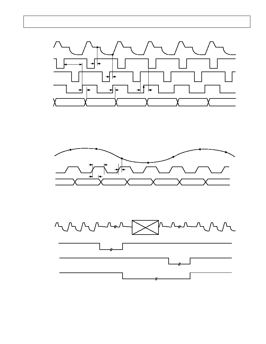
TIMING SPECIFICATIONS
N
N+1
N+2
N+3
N+4
t
INHIBIT
t
ID
t
ID
t
OD
t
HOLD
ADCCLK RISING EDGE PLACEMENT
N8
N7
N6
N5
N4
N3
CCD
SHP
SHD
ADCCLK
D0D9
NOTES:
1. SHP AND SHD SHOULD BE OPTIMALLY ALIGNED WITH THE CCD SIGNAL. SAMPLES ARE TAKEN AT THE
RISING EDGES.
2. ADCCLK RISING EDGE MUST OCCUR AT LEAST 15ns AFTER THE RISING EDGE OF SHP (
t
INHIBIT
).
3. RECOMMENDED PLACEMENT FOR ADCCLK RISING EDGE IS BETWEEN THE RISING EDGE OF SHD AND FALLING EDGE OF SHP.
4. OUTPUT LATENCY (7 CYCLES) SHOWN WITH EVEN-ODD OFFSET CORRECTION ENABLED.
5. ACTIVE LOW CLOCK PULSE MODE IS SHOWN.
Figure 1. CCD-MODE Timing
t
ID
t
OD
t
HOLD
N
N+1
N+2
N+3
N+4
N4
N3
N2
N+5
VIDEO
INPUT
ADCCLK
D0D9
N1
N
NOTE:
EXAMPLE OF OUTPUT DATA LATCHED BY ADCCLK RISING EDGE.
Figure 2. AUX-MODE and ADC-MODE Timing
CCD
SIGNAL
CLPOB
CLPDM
PBLK
EFFECTIVE
PIXELS
OPTICAL BLACK
BLANKING
INTERVAL
DUMMY BLACK
EFFECTIVE
PIXELS
NOTES:
1. CLPOB PULSEWIDTH SHOULD BE A MINIMUM OF 10 OB PIXELS WIDE, 20 OB PIXELS ARE RECOMMENDED.
2. CLPDM PULSEWIDTH SHOULD BE AT LEAST 1 s WIDE.
3. PBLK IS NOT REQUIRED, BUT RECOMMENDED IF THE CCD SIGNAL AMPLITUDE EXCEEDS 1V p-p.
4. CLPDM OVERWRITES PBLK.
5. ACTIVE LOW CLAMP PULSE MODE IS SHOWN.
Figure 3. CCD-MODE Clamp Timing
AD9803
6
REV. 0
ORDERING GUIDE
Model
Temperature Range
Package Description
Package Option
AD9803JST
0
°
C to +70
°
C
48-Lead Plastic Thin Quad Flatpack
ST-48
CAUTION
ESD (electrostatic discharge) sensitive device. Electrostatic charges as high as 4000 V readily
accumulate on the human body and test equipment and can discharge without detection.
Although the AD9803 features proprietary ESD protection circuitry, permanent damage may
occur on devices subjected to high energy electrostatic discharges. Therefore, proper ESD
precautions are recommended to avoid performance degradation or loss of functionality.
WARNING!
ESD SENSITIVE DEVICE
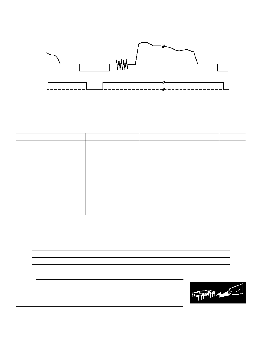
TIMING SPECIFICATIONS (CONTINUED)
H
SYNC
MANUAL CLAMPING
AUTOMATIC CLAMPING
VIDEO
SIGNAL
ACLP
Figure 4. AUX-MODE Clamp Timing
NOTE: ACLP can be used two different ways. To control the
exact time of the clamp, an active low pulse is used to specify
the clamp interval. Alternatively, ACLP may be tied to ground.
In this configuration, the clamp circuitry will sense the most
negative portion of the signal and use this level to set the clamp
voltage. For the video waveform in Figure 4, the SYNC level
will be clamped to the black level specified in the E-Register.
Active low clamp pulse mode is shown.
ABSOLUTE MAXIMUM RATINGS*
Parameter
With Respect To
Min
Max
Units
ADVDD
ADVSS, SUBST
0.3
6.5
V
ACVDD
ACVSS, SUBST
0.3
6.5
V
DVDD
DVSS
0.3
6.5
V
DRVDD
DRVSS
0.3
6.5
V
CLOCK INPUTS
DVSS
0.3
DVDD + 0.3
V
PGACONT1, PGACONT2
SUBST
0.3
ACVDD + 0.3
V
PIN, DIN
SUBST
0.3
ACVDD + 0.3
V
DOUT
DRVSS
0.3
DRVDD + 0.3
V
VRT, VRB
SUBST
0.3
ADVDD + 0.3
V
CCDBYP1, CCDBYP2
SUBST
0.3
ACVDD + 0.3
V
DAC1, DAC2
SUBST
0.3
ACVDD + 0.3
V
DRVSS, DVSS, ACVSS, ADVSS
SUBST
0.3
+0.3
V
Junction Temperature
+150
°
C
Storage Temperature
65
+150
°
C
Lead Temperature (10 sec)
+300
°
C
*Stresses above those listed under Absolute Maximum Ratings may cause permanent damage to the device. This is a stress rating only; functional operation of the device
at these or other conditions above those indicated in the operational sections of this specification is not implied. Exposure to absolute maximum ratings for extended periods
may affect device reliability.
AD9803
7
REV. 0
PIN FUNCTION DESCRIPTIONS
P
in #
Pin Name
Type
Description (See Figures 37 and 38 for Circuit Configurations)
1, 24
NC
No Connect (Should be Left Floating or Tied to Ground)
211
D0D9
DO
Digital Data Outputs
12
DRVDD
P
Digital Driver Supply (3 V)
13
DRVSS
P
Digital Driver Ground
14
DVSS
P
Digital Ground
15
ACLP
P
AUX-MODE/ADC-MODE Clamp
16
ADCCLK
DI
ADC Sample Clock Input
17
DVDD
P
Digital Supply (3 V)
18
STBY
DI
Power-Down Mode (Active Hi/Internal Pull-Down). Enables Reference Stand-By Mode.
19
PBLK
DI
Pixel Blanking
20
CLPOB
DI
Black Level Restore Clamp
21
SHP
DI
CCD Reference Sample Clock Input
22
SHD
DI
CCD Data Sample Clock Input
23
CLPDM
DI
Input Clamp
25
CCDBYP2
AO
CDS Ground Bypass (0.1
µ
F to Ground)
26
DIN
AI
CDS Negative Input (Tie to Pin 27 and AC-Couple to CCD Input Signal)
27
PIN
AI
CDS Positive Input (See Above)
28
CCDBYP1
AO
CDS Ground Bypass (0.1
µ
F to Ground)
29
PGACONT1
AI
PGA Coarse Gain Analog Control
30
PGACONT2
AI
PGA Fine Gain Analog Control
31
ACVSS
P
Analog Ground
32
CLPBYP
AO
Bias Bypass (0.1
µ
F to Ground)
33
ACVDD
P
Analog Supply (3 V)
34
AUXIN
AI
AUX-MODE Input
35
AUXCONT
AI
AUX-MODE PGA Gain Analog Control
36
ADCIN
AI
ADC-MODE Input
37
CMLEVEL
AO
Common-Mode Level (0.1
µ
F to Ground)
38
VTRBYP
AO
Bias Bypass (0.1
µ
F to Ground)
39
DAC1
AO
DAC1 Output
40
DAC2
AO
DAC2 Output
41
SL
DI
Serial I/F Load Signal
42
SCK
DI
Serial I/F Clock
43
ADVDD
P
Analog Supply (3 V)
44
SDATA
DI
Serial I/F Input Data
45
ADVSS
P
Analog Ground
46
SUBST
P
Analog Ground
47
VRB
AO
Bottom Reference (0.1
µ
F to Ground and 1
µ
F to VRT)
48
VRT
AO
Top Reference (0.1
µ
F to Ground)
NOTE
Type: AI = Analog Input, AO = Analog Output, DI = Digital Input, DO = Digital Output, P = Power.
PIN CONFIGURATION
36
35
34
33
32
31
30
29
28
27
26
25
13 14 15 16 17 18 19 20 21 22 23 24
1
2
3
4
5
6
7
8
9
10
11
12
48 47 46 45 44
39 38 37
43 42 41 40
PIN 1
IDENTIFIER
TOP VIEW
(Not to Scale)
DVDD
DVSS
ACLP
ADCCLK
STBY
NC
(LSB) D0
D1
D2
D3
D4
D5
D6
D7
D8
(MSB) D9
DRVDD
PBLK
CLPOB
SHP
SHD
AD9803
NC
ADCIN
AUXCONT
AUXIN
ACVDD
CLPBYP
ACVSS
PGACONT2
PGACONT1
CCDBYP1
PIN
DIN
CCDBYP2
VRT
VRB
SUBST
ADVSS
SDATA
ADVDD
SCK
SL
DAC2
DAC1
VTRBYP
CMLEVEL
CLPDM
DRVSS
NC = NO CONNECT
AD9803
8
REV. 0
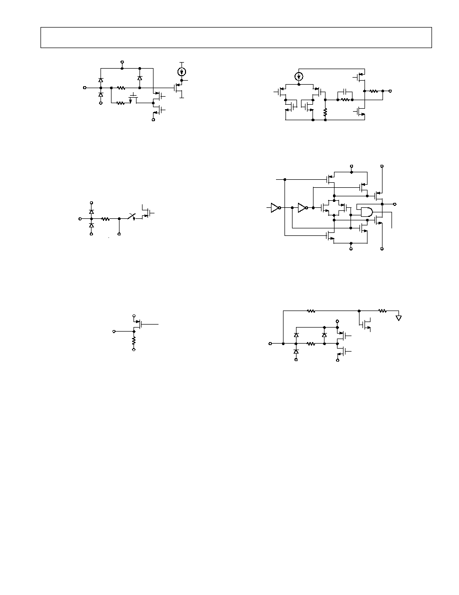
EQUIVALENT INPUT CIRCUITS
DVDD
DRVDD
DVSS
DRVSS
Figure 5. Pins 211 (D0D9)
DVDD
DVSS
200
DVSS
Figure 6. Pin 16, 21, 22 (ADCCLK, SHP, SHD)
ACVDD
SUBST
ACVSS
50
Figure 7. Pins 25, 28 (CCDBYP)
ACVDD
SUBST
ACVSS
50
10pF
Figure 8. Pin 26 (DIN) and Pin 27 (PIN)
ACVDD
SUBST
PGACONT1
1k
CMLEVEL
8k
8k
10k
PGACONT2
OPEN ANALOG CONTROL
CLOSED DIGITAL CONTROL
Figure 9. Pin 29 (PGACONT1) and Pin 30 (PGACONT2)
ACVDD
SUBST
ACVSS
10k
30k
200
Figure 10. Pin 32 (CLPBYP)
AD9803
9
REV. 0
ACVDD
SUBST
ACVSS
50
50
Figure 11. Pin 34 (AUXIN) and Pin 36 (ADCIN)
ACVDD
SUBST
CMLEVEL
5.5k
OPEN ANALOG CONTROL
CLOSED DIGITAL CONTROL
Figure 12. Pin 35 (AUXCONT)
ADVDD
ADVSS
9.3k
Figure 13. Pin 37 (CMLEVEL)
ADVDD
INTERNAL
DAC OUT
ADVSS
39k
39k
1.4pF
70
DAC1, DAC2
OUTPUT
Figure 14. Pin 39 (DAC1) and 40 (DAC2)
DVDD
DRVDD
DVSS
DRVSS
DATA
IN
SDATA
DATA
OUT
RNW
Figure 15. Pin 44 (SDATA)
ADVDD
SUBST
ADVSS
3k
200
1.1k
Figure 16. Pin 47 (VRB) and Pin 48 (VRT)
AD9803
10
REV. 0
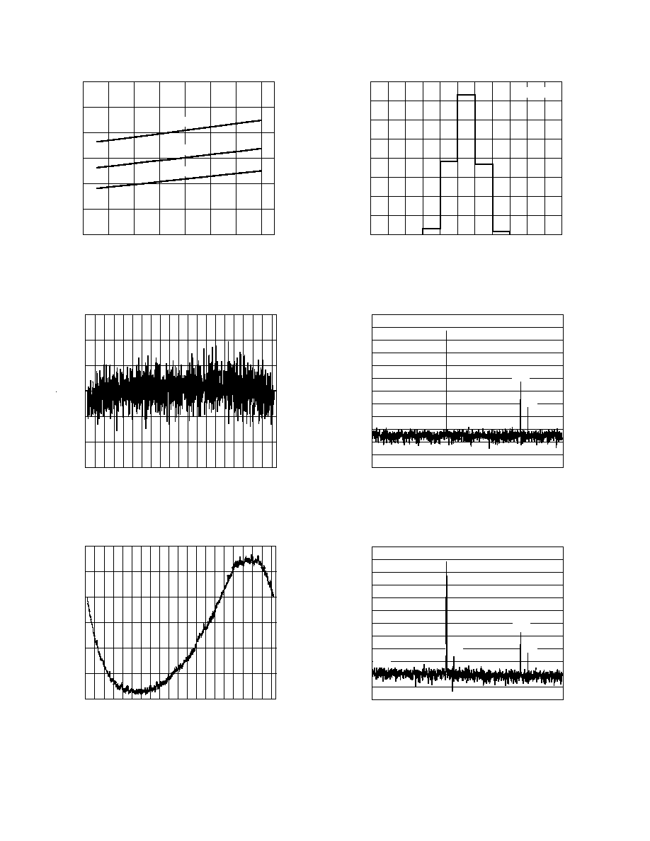
Typical Performance Characteristics
SAMPLE RATE MHz
240
4
POWER DISSIPATION mV
220
200
180
160
140
120
6
8
10
12
14
16
18
V
DD
= 3.3V
V
DD
= 3.0V
V
DD
= 2.8V
Figure 17. CCD-MODE Power vs. Clock Rate
TITLE
TITLE
0.6
0
0.4
0.2
0.0
0.2
0.4
0.6
150
300
450
600
750
900
1023
Figure 18. CCD-MODE DNL at 18 MHz
0
4
2
0
2
4
6
150
300
450
600
750
900
1023
8
Figure 19. CCD-MODE INL at 18 MHz
DIGITAL OUTPUT CODE Decimal
800000
29
NUMBER OF HITS
700000
600000
500000
400000
300000
200000
100000
0
30
31
32
33
34
35
36
37
38
39
= 0.8 LSB
Figure 20. CCD-MODE Grounded-Input Noise
(PGA Gain = MIN)
FREQUENCY MHz
60
DC
dB
1
2
3
4
5
6
7
8
9
50
40
30
20
10
0
10
20
30
40
50
60
5TH
4TH
2ND
3RD
FUND
THD = 38.7dB
Figure 21. AUX-MODE THD at 18 MHz
(f
IN
= 3.54 MHz at 3 dB)
FREQUENCY MHz
60
DC
dB
1
2
3
4
5
6
7
8
9
50
40
30
20
10
0
10
20
30
40
50
60
2ND
3RD
FUND
THD = 54.1dB
4TH
5TH
Figure 22. ADC-MODE at 18 MHz
(f
IN
= 3.54 MHz at 3 dB)
AD9803
11
REV. 0
THEORY OF OPERATION
Introduction
The AD9803 is a 10-bit analog-to-digital interface for CCD
cameras. The block level diagram of the system is shown in
Figure 23. The device includes a correlated double sampler
(CDS), 0 dB30 dB programmable gain amplifier (PGA), black
level correction loop, input clamp and voltage reference. The
only external analog circuitry required at the system level is an
emitter follower buffer between the CCD output and AD9803
inputs.
CLPDM
INPUT CLAMP
PIN
DIN
CDS
SHA
ADC
INTEG
BLACK LEVEL CLAMP
PGA
DIFFERENTIAL SIGNAL PATH
CLPOB
Figure 23. CCD Mode Signal Path
Correlated Double Sampling (CDS)
CDS is important in high performance CCD systems as a
method for removing several types of noise. Basically, two
samples of the CCD output are taken: one with the signal
present ("data") and one without ("reference"). Subtracting
these two samples removes any noise which is common--or
correlated--to both.
Figure 24 shows the block diagram of the AD9803's CDS. The
S/H blocks are directly driven by the input and the sampling
function is performed passively, without the use of amplifiers.
This implementation relies on the off-chip emitter follower
buffer to drive the two 10 pF sampling capacitors. Only one
capacitor at a time is seen at the input pin.
10pF
Q1
S/H
Q2
S/H
S
OUT
FROM
CCD
Figure 24. CDS Block Diagram
The AD9803 actually uses two CDS circuits in a "ping pong"
fashion to allow the system more acquisition time. In this way,
the output from one of the two CDS blocks will be valid for an
entire clock cycle. Thus, the bandwidth requirement of the
subsequent gain stage is reduced as compared to that for a single-
channel CDS system. This lower bandwidth translates to lower
power and noise.
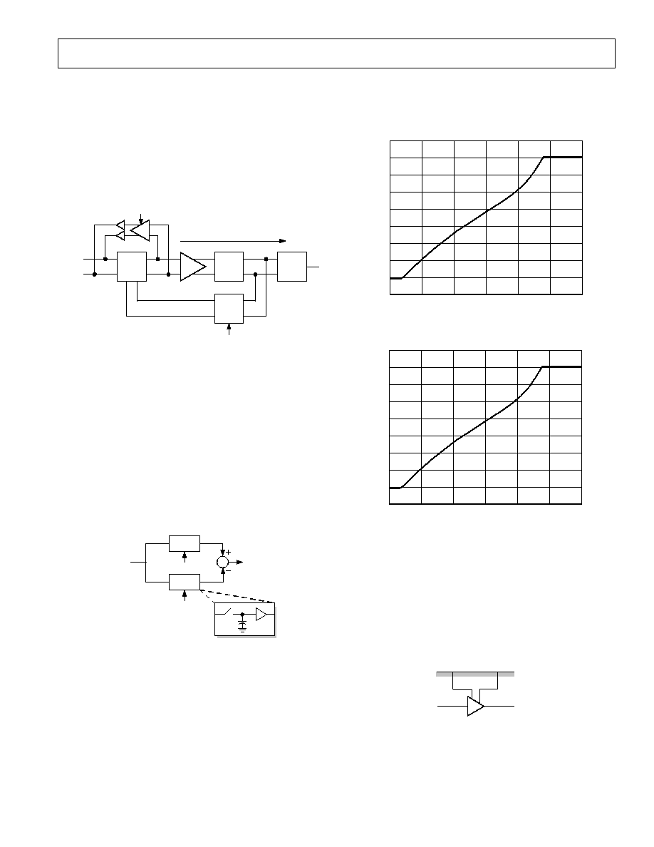
Programmable Gain Amplifier (PGA)
The on-chip PGA provides a gain range of 0 dB30 dB, which
is "linear in dB." Typical gain characteristics are shown in
Figures 25 and 26.
40
GAIN dB
PGACONT1 Volts
0
35
30
25
20
15
10
5
0
5
0.5
1.0
1.5
2.0
2.5
3.0
Figure 25. PGA Gain Curve--Analog Control
40
GAIN dB
PGA GAIN REGISTER
0
35
30
25
20
15
10
5
0
5
1023
171
341
511
682
852
Figure 26. PGA Gain Curve--Digital Control
As shown in Figure 27, analog PGA control is provided through
the PGACONT1 and PGACONT2 inputs. PGACONT1 pro-
vides coarse and PGACONT2 fine (1/16) gain control. The
PGA gain can also be controlled using the internal 10-bit DAC
through the serial digital interface. The gain characteristic
shown in Figure 26, with the internal DAC providing the same
control range as PGACONT1. See the Serial Interface Specifi-
cations for more details.
A
PGACONT1
PGACONT2
PGACONT1 = COARSE CONTROL
PGACONT2 = FINE (1/16) CONTROL
Figure 27. Analog PGA Control
AD9803
12
REV. 0
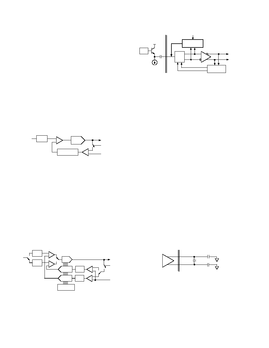
Black Level Clamping
For correct signal processing, the CCD signal must be refer-
enced to a well established "black level." The AD9803 uses the
CCD's optical black (OB) pixels as a calibration signal, which is
used to establish the black level. Two sources of offset are
addressed during the calibration--the CCD's own "black level"
offset, and the AD9803's internal offsets in the CDS and PGA
circuitry.
The feedback loop shown in Figure 28 is closed around the
PGA during the calibration interval (CLPOB = LOW) to set
the black level. As the black pixels are being processed, an inte-
grator block measures the difference between the input level
and the desired reference level. This difference, or error, signal
is amplified and passed to the CDS block where it is added to
the incoming pixel data. As a result of this process, the black
pixels are digitized at one end of the ADC range, taking maxi-
mum advantage of the available linear range of the system.
Using the AD9803's serial digital interface, the black level
reference may programmed to 16 LSB, 32 LSB, 48 LSB, or
64 LSB.
PGA
ADC
IN
CLPOB
NEG REF
INTEGRATOR
CDS
Figure 28. Black Level Correction Loop (Simplified)
The actual implementation of this loop is slightly more compli-
cated as shown in Figure 29. Because there are two separate
CDS blocks, two black level feedback loops are required and
two offset voltages are developed. Figure 29 also shows an
additional PGA block in the feedback loop labeled "RPGA."
The RPGA uses the same control inputs as the PGA, but has
the inverse gain. The RPGA functions to attenuate by the same
factor as the PGA amplifies, keeping the gain and bandwidth of
the loop constant.
There exists an unavoidable mismatch in the two offset voltages
used to correct both CDS blocks. This mismatch causes a
slight difference in the offset level for odd and even pixels, often
called "pixel-to-pixel offset" or "even-odd offset." To compen-
sate for this mismatch, the AD9803 uses a digital correction
circuit after the ADC which removes the even-odd offset be-
tween the channels.
PGA
ADC
IN
CLPOB
NEG REF
CONTROL
CDS1
RPGA2
INT2
CDS2
RPGA1
INT1
Figure 29. Black Level Correction Loop (Detailed)
Input Bias Level Clamping
The buffered CCD output is connected to the AD9803 through
an external coupling capacitor. The dc bias point for this cou-
pling capacitor is established during the clamping (CLPDM =
LOW) period using the "dummy clamp" loop shown in Figure
30. When closed around the CDS, this loop establishes the
desired dc bias point on the coupling capacitor.
BLACK
LEVEL CLP
CCD
INPUT
CLAMP
CLPDM
TO ADC
PGA
CDS
Figure 30. Input Clamp
Input Blanking
In some applications, the AD9803's input may be exposed to
large signals from the CCD, either during blanking intervals or
"high speed" modes. If the signals are larger than the AD9803's
1 V p-p input signal range, then the on-chip input circuitry
may saturate. Recovery time from a saturated state could be
substantial.
To avoid problems associated with processing these large tran-
sients, the AD9803 includes an input blanking function. When
active (PBLK = LOW) this function stops the CDS operation
and allows the user to disconnect the CDS inputs from the
CCD buffer. Additionally, the AD9803's digital outputs will all
go to zero while PBLK is low.
If the input voltage exceeds the supply rail by more than
0.3 volts, then protection diodes will be turned on, increasing
current flow into the AD9803 (see Equivalent Input Circuits).
Such voltage levels should be externally clamped to prevent
possible device damage.
10-Bit Analog-to-Digital Converter (ADC)
The ADC employs a multibit pipelined architecture which is
well-suited for high throughput rates while being both area and
power efficient. The multistep pipeline presents a low input
capacitance resulting in lower on-chip drive requirements. A
fully differential implementation was used to overcome head-
room constraints of the single +3 V power supply.
Differential Reference
The AD9803 includes a 0.5 V reference based on a differential,
continuous-time bandgap cell. Use of an external bypass capaci-
tor reduces the reference drive requirements, thus lowering the
power dissipation. The differential architecture was chosen for
its ability to reject supply and substrate noise. Required decou-
pling is shown in Figure 31.
VRT
REF
VRB
1 F
0.1 F
0.1 F
Figure 31. Reference Decoupling
Internal Timing
The AD9803's on-chip timing circuitry generates all clocks
necessary for operation of the CDS and ADC blocks. The user
needs only to synchronize the SHP and SHD clocks with the
CCD waveform, as all other timing is handled internally. The
ADCCLK signal is used to strobe the output data, and can be
adjusted to accommodate desired timing. Figure 1 shows the
recommended placement of ADCCLK relative to SHP and
SHD.
AD9803
13
REV. 0
Even-Odd Pixel Offset Correction
The AD9803 includes digital correction circuitry following the
10-bit ADC. The purpose of the digital correction is remove
the residual offset between the even and odd pixel channels,
which results from the "ping-pong" CDS architecture of the
AD9803. The digital offset correction tracks the black level of
the even and odd channels, applying the necessary digital cor-
rection value to keep them balanced. There is an additional two
cycle delay when using the offset correction, resulting in pipe-
line delay of 7 ADCCLK cycles (see Figure 1).
A/D
CONVERTER
+
EVEN
ODD
2:1
MUX
ADCCLK
10
DIGITAL
OFFSET
CORRECTION
DOUT
CLPOB
Figure 32. Digital Offset Correction
Auxiliary DACs
The AD9803 includes two 8-bit DACs for controlling any off-
chip system functions. These are voltage output DACs with
near rail-to-rail output capability. Output voltage levels are
programmed through the serial interface. DAC specifications
are shown on page 4, and the DAC equivalent output circuit is
shown in Figure 14.
AUX-MODE Operation
In addition to the CCD signal-processing path, the AD9803
includes an analog video-processing path. The AUXIN (Pin 34)
input consists of an input clamp, PGA, and ADC. Figure 33
shows the Input Configuration of this mode. The recommended
value of the external ac-coupling capacitor is 0.1
µ
F. The volt-
age droop with this capacitor value is 20
µ
V/
µ
s.
The recommended method of controlling the input clamp is
to simply ground the ACLP input (Pin 15) to activate the
"automatic" clamping capability of the AD9803. The clamp
may also be controlled with a separate clock signal. See the
clamp timing in Figure 4 for more details.
The THD performance for f
S
= 18 MHz is shown in Figure 21.
When operating at f
S
= 18 MHz, the linearity performance is
comparable to the CCD-Mode linearity, shown in Figure 18.
The AUX-MODE can be operated at a sampling rate of up to
28.6 MHz. If the sample rate exceeds 18 MHz, then the High
Speed AUX-MODE should be programmed through the serial
interface (D-Register 01).
AUXIN
CLP
ACLP
PGA
SHA
CLAMP LEVEL (E-REG)
+
0.1 F
VIDEO
SIGNAL
GND
AD9803
0~10 dB
ADCCLK
2 A
ADC
LPF
34
15
16
AUX
CONT
35
0.1 F
Figure 33. AUX-MODE Circuit Configuration
ADC-MODE Operation
The ADC-MODE of operation is the same as the AUX-MODE,
except there is no PGA in the signal path, only the input clamp
and ADC. Input specifications and timing for ADC-MODE are
the same as those for AUX-MODE. The THD performance is
shown in Figure 22.
AD9803
14
REV. 0
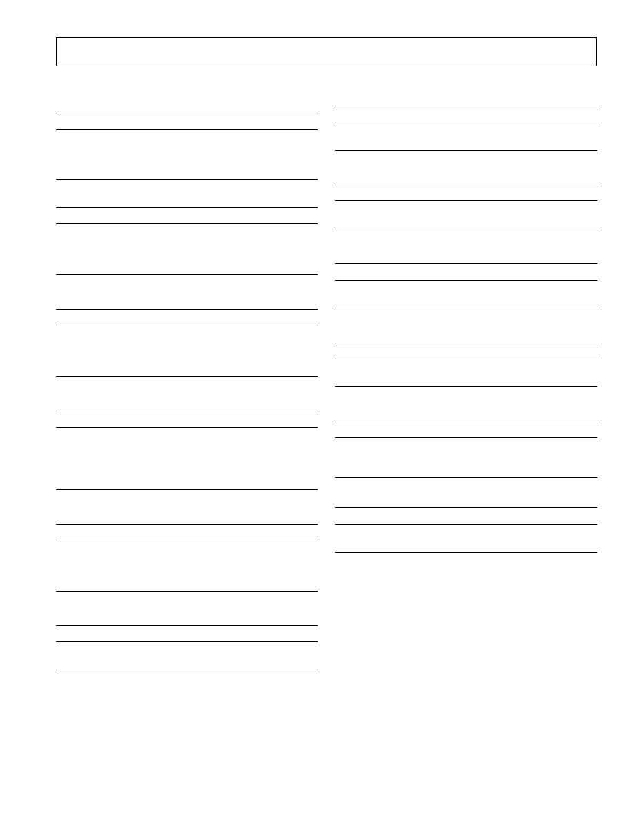
SERIAL INTERFACE SPECIFICATIONS
MODES2
1
SDATA
SELECT
DAC2
DAC1
PGA
MODES
A0
1
0
1
0
1
A1
1
0
1
1
0
A2
1
1
0
0
0
D0
D1
D2
D3
D4
D5
D6
D7
D8
D9
e0
e1
d0
d1
c0
c1
b0
b1
a0
a1
CLAMP
LEVEL
POWER DOWN
MODES
CLOCK
MODES
OUTPUT
MODES
OPERATION
MODES
f0
f1
f2
f3
f4
f5
f6
f7
f8
f9
PGA GAIN LEVEL SELECTION
g0
g1
g2
g3
g4
g5
g6
g7
h0
h1
h2
h3
h4
h5
h6
h7
m0
0
k0
j0
DAC1 INPUT
DAC2 INPUT
OPERATION AND
POWER DOWN MODES
SHIFT REGISTER
F-REG
f0f9
E-REG
e0e1
D-REG
(d) POWER DOWN MODES
d0d1
C-REG
c0c1
B-REG
b0b1
A-REG
(a) OPERATION MODES
a0a1
(b) OUTPUT MODES
(c) CLOCK MODES
(e) CLAMP LEVEL
(f) PGA GAIN
M-REG
m0
K-REG
(k) EXTERNAL PGA
GAIN CONTROL
k0
J-REG
j0
H-REG
h0h7
G-REG
(g) DAC1 INPUT
g0g7
(h) DAC2 INPUT
(j) EVEN-ODD OFFSET
CORRECTION
(m) DAC1 AND DAC2
POWER DOWN
SELECT
NOTE
1
MODES2 REGISTER BIT D1 MUST
BE SET TO ZERO.
Figure 34. Internal Register Map
RISING EDGE
TRIGGERED
t
DH
t
LS
t
LH
REGISTER LOADED ON
RISING EDGE
RNW
A0
A1
A2
D0
D1
D2
D3
D4
D5
D6
D7
D8
D9
SDATA
SCK
SL
t
DS
Figure 35. Serial WRITE Operation
SDATA
RNW
A0
A1
A2
D0
D1
D2
D3
D4
D5
D6
D7
D8
D9
XX
XX
DUMMY BITS
IGNORED
SCK
SL
Figure 36. 16-Bit Serial WRITE Operation
AD9803
15
REV. 0
REGISTER DESCRIPTION
(a) A-REGISTER: Modes of Operation (Power-On Default
Value = 11)
a1
a0
Modes
0
0
ADC-MODE
0
1
AUX-MODE
1
0
CCD-MODE
1
1
CCD-MODE
(b) B-REGISTER: Output Modes (Default = 00)
b1
b0
D9 D8 D7 D6 D5 D4 D3 D2 D1 D0
0
0
Normal
0
1
0
1
0
1
0
1
0
1
0
1
1
0
1
0
1
0
1
0
1
0
1
0
1
1
High Impedance
(c) C-REGISTER: Clock Modes (Default = 00)
c1
c0
SHP-SHD Clock Pulses
Clamp Active Pulses
0
0
Active Low
Active Low
0
1
Active Low
Active High
1
0
Active High
Active Low
1
1
Active High
Active High
(d) D-REGISTER: Power-Down Modes (Default = 00)
Modes
d1
d0 Description
Normal
0
0
Normal Operation
High Speed
0
1
High Speed AUX-MODE
Power-Down 1
1
0
Reference Stand-By (Same Mode
as STBY Pin 18)
Power-Down 2
1
1
Total Shut-Down
(e) E-REGISTER: Clamp Level Selection (Default = 00)
e1
e0
Clamp Level
CLP (0)
0
0
32 LSBs
CLP (1)
0
1
48 LSBs
CLP (2)
1
0
64 LSBs
CLP (3)
1
1
16 LSBs
(f) F-REGISTER: PGA Gain Selection (Default = 00 . . . 0)
f 9 f 8 f 7 f 6 f 5 f 4 f 3 f 2 f 1 f 0
CCD-Gain
Gain (0)
0 0 0 0 0 0 0 0 0 0
Minimum
Gain (1023) 1 1 1 1 1 1 1 1 1 1
Maximum
(f) F-REGISTER: PGA Gain Selection (Default = 00 . . . 0)
f 9 f 8 f 7 f 6 f 5 f 4 f 3 f 2
AUX-Gain
Gain (0)
0 0 0 0 0 0 0 0
Minimum
Gain (255)
1 1 1 1 1 1 1 1
Maximum
(g) G-REGISTER: DAC1 Input (Default = 00 . . . 0)
g7 g6 g5 g4 g3 g2 g1 g0
DAC1 Output
Code (0)
0
0
0
0
0
0
0
0
Minimum
Code (255) 1
1
1
1
1
1
1
1
Maximum
(h) H-REGISTER: DAC2 Input (Default = 00 . . . 0)
h7 h6 h5 h4 h3 h2 h1 h0
DAC2 Output
Code (0)
0
0
0
0
0
0
0
0
Minimum
Code (255) 1
1
1
1
1
1
1
1
Maximum
(j) J-REGISTER: Even-Odd Offset Correction (Default = 0)
j0
Even-Odd Offset Correction
0
Offset Correction In Use
1
Offset Correction Not Used
(k) K-REGISTER: External PGA Gain Control (Default = 0)
k0
PGA Gain Control
0
External Voltage Control Through AUXCONT or
PGACONT1 and PGACONT2
1
Internal 10-Bit DAC Control of PGA Gain
(m) M-REGISTER: DAC1 & DAC2 pdn (Default = 0)
m0
Power-Down of 8-Bit DACs
0
8-Bit DACs Powered-Down
1
8-Bit DACs Operational
AD9803
16
REV. 0
NOTE: With the exception of a write to the PGA register dur-
ing AUX-mode, all data writes must be 10 bits. During an
AUX-mode write to the PGA register, only 8 bits of data are
required. If more than 14 SCK rising edges are applied during a
write operation, additional SCK pulses will be ignored (see
Figure 35). All reads must be 10 bits to receive valid register
contents. All registers default to 0s on power-up, except for the
A-register which defaults to 11. Thus, on power-up, the AD9803
defaults to CCD mode. During the power-up phase, it is recom-
mended that SL be HIGH and SCK be LOW to prevent acci-
dental register write operations. SDATA may be unknown. The
RNW bit ("Read/Not Write") must be LOW for all write opera-
tions to the serial interface, and HIGH when reading back from
the serial interface registers.
APPLICATIONS INFORMATION
Power and Grounding Recommendations
The AD9803 should be treated as an analog component when
used in a system. The same power supply and ground plane
should be used for all of the pins. In a two-ground system, this
requires that the digital supply pins be decoupled to the analog
ground plane and the digital ground pins be connected to ana-
log ground for best noise performance. Separate digital supplies
can be used, particularly if slightly different driver supplies are
needed, but the digital power pins should still be decoupled to
the same point as the digital ground pins (the analog ground
plane). If the AD9803 digital outputs need to drive a bus or
substantial load, then a buffer should be used at the AD9803's
outputs, with the buffer referenced to system digital ground. In
some cases, when system digital noise is not substantial, it is
acceptable to split the ground pins on the AD9803 to separate
analog and digital ground planes. If this is done, be sure to
connect the two ground planes together at the AD9803.
To further improve performance, isolating the driver supply
DRVDD from DVDD with a ferrite bead can help reduce kick-
back effects during major code transitions. Alternatively, the
use of damping resistors on the digital outputs will reduce the
output rise times, also reducing the kickback effect.
Application Circuit Utilizing the AD9803's Digital Gain Control
Figure 37 shows the recommended circuit configuration for
CCD-Mode operation when using the 3-wire serial interface.
The analog PGA control pins, PGACONT1 and PGACONT2,
should be shorted together and decoupled to ground. If the two
auxiliary DACs are not used, then Pins 39 and 40 (DAC1 and
DAC2) may be grounded.
Using the AD9803 in AD9801 Sockets
The AD9803 may be easily used in existing AD9801 designs
without any circuit modifications. Most of the pin assignments
are the same for both ICs. Table I outlines the differences. The
circuit of Figure 38 shows the necessary connections for the
AD9803 when used in an existing AD9801 socket. The power-
on reset in the AD9803 assures that the device will power-up in
CCD-mode, with analog PGA gain control.
Table I. AD9801/AD9803 Pin Differences
Pin
No.
AD9801
AD9803
AD9801 Connection
1
ADVSS
NC
Ground
14
DSUBST
DVSS
Ground
15
DVSS
ACLP
Ground
24
DVSS
NC
Ground
32
CLAMP_BIAS
CLPBYP
Decoupled with 0.1
µ
F
to Ground
34
ACVDD
AUXIN
+3 Volt Supply
35
ACVDD
AUXCONT
+3 Volt Supply
36
INT_BIAS1
ADCIN
Decoupled with 0.1
µ
F
to Ground
38
INT_BIAS2
VTRBYP
Decoupled with 0.1
µ
F
to Ground
39
MODE2
DAC1
Ground
40
MODE1
DAC2
Ground
41
ADVSS
SL
Ground
42
ADVDD
SCK
+3 Volt Supply
44
ADVSS
SDATA
Ground
AD9803
17
REV. 0
0.1 F
0.1 F
0.1 F
0.1 F
0.1 F
CCD
SIGNAL
INPUT
V
DD
0.1 F
DIGITAL
OUTPUT
DATA
48
47
46
45
44
39 38
37
43
42
41 40
1
2
3
4
5
6
7
8
9
10
11
12
NC
D0 (LSB)
D1
D2
D3
D4
D5
D6
D7
D8
D9 (MSB)
DRVDD
AD9803
13 14
15
16
17
18
19
20
21 22
23
24
DVDD
DVSS
ACLP
ADCCLK
STBY
PBLK
CLPOB
SHP
SHD
NC
VRT
VRB
SUBST
ADVSS
SDATA
ADVDD
SCK
SL
DAC2
DAC1
VTRBYP
CMLEVEL
CLPDM
DRVSS
36
35
34
33
32
31
30
29
28
27
26
25
ADCIN
AUXCONT
AUXIN
ACVDD
CLPBYP
ACVSS
PGACONT2
PGACONT1
CCDBYP1
PIN
DIN
CCDBYP2
NC = NO CONNECT
0.1 F
V
DD
V
DD
0.1 F
CLPDM
SHD
SHP
CLPOB
PBLK
ADCCLK
0.1 F
0.1 F
VOUT1
VOUT2
SDATA
SCK
SL
0.1 F
0.1 F
1.0 F
0.1 F
V
DD
Figure 37. CCD-Mode Circuit Configuration--Digital PGA Control
AD9803
18
REV. 0
DIGITAL
OUTPUT
DATA
48
47
46
45
44
39 38
37
43
42
41 40
1
2
3
4
5
6
7
8
9
10
11
12
NC
D0 (LSB)
D1
D2
D3
D4
D5
D6
D7
D8
D9 (MSB)
DRVDD
AD9803
13 14
15
16
17
18
19
20
21 22
23
24
DVDD
DVSS
ACLP
ADCCLK
STBY
PBLK
CLPOB
SHP
SHD
NC
VRT
VRB
SUBST
ADVSS
SDATA
ADVDD
SCK
SL
DAC2
DAC1
VTRBYP
CMLEVEL
CLPDM
DRVSS
36
35
34
33
32
31
30
29
28
27
26
25
ADCIN
AUXCONT
AUXIN
ACVDD
CLPBYP
ACVSS
PGACONT2
PGACONT1
CCDBYP1
PIN
DIN
CCDBYP2
NC = NO CONNECT
0.1 F
V
DD
V
DD
0.1 F
CLPDM
SHD
SHP
CLPOB
PBLK
ADCCLK
0.1 F
0.1 F
0.1 F
CCD SIGNAL INPUT
0.1 F
0.1 F
0.1 F
0.1 F
0.1 F
1.0 F
0.1 F
V
DD
STBY
PGACONT1
PGACONT2
V
DD
0.1 F
0.1 F
0.1 F
0.1 F
Figure 38. Recommended Circuit for AD9801 Sockets
AD9803
19
REV. 0
OUTLINE DIMENSIONS
Dimensions shown in inches and (mm).
48-Lead Plastic Thin Quad Flatpack (LQFP)
(ST-48)
0.354 (9.00) BSC
0.276 (7.0) BSC
1
12
13
25
24
36
37
48
TOP VIEW
(PINS DOWN)
0.276 (7.0) BSC
0.354 (9.00) BSC
0.009 (0.225)
0.006 (0.17)
0.019 (0.5)
BSC
SEATING
PLANE
0.063 (1.60) MAX
0° MIN
0° 7°
0.076 MAX
NO MIN
0.030 (0.75)
0.018 (0.45)
0.057 (1.45)
0.053 (1.35)
0.030 (0.75)
0.018 (0.45)
0.007 (0.18)
0.004 (0.09)