 | ÐлекÑÑоннÑй компоненÑ: AD9801 | СкаÑаÑÑ:  PDF PDF  ZIP ZIP |
Äîêóìåíòàöèÿ è îïèñàíèÿ www.docs.chipfind.ru
REV. 0
Information furnished by Analog Devices is believed to be accurate and
reliable. However, no responsibility is assumed by Analog Devices for its
use, nor for any infringements of patents or other rights of third parties
which may result from its use. No license is granted by implication or
otherwise under any patent or patent rights of Analog Devices.
a
AD9801
One Technology Way, P.O. Box 9106, Norwood, MA 02062-9106, U.S.A.
Tel: 617/329-4700
World Wide Web Site: http://www.analog.com
Fax: 617/326-8703
© Analog Devices, Inc., 1997
CCD Signal Processor
For Electronic Cameras
FUNCTIONAL BLOCK DIAGRAM
SHP
AD9801
PGA
PGACONT1 PGACONT2
CLAMP
CLPDM
CDS
PBLK
PIN
DIN
SHD ADCCLK
TIMING
GENERATOR
23
29
30
19
21
22
16
27
26
37
48
47
18
CMLEVEL VRT VRB STBY
REFERENCE
S/H
20
CLPOB
CLAMP
A/D
2
11
DOUT
33
ACVDD
43
ADVDD
17
DVDD
12
DRVDD
10
FEATURES
10-Bit, 18 MSPS A/D Converter
18 MSPS Full-Speed CDS
Low Noise, Wideband PGA
Internal Voltage Reference
No Missing Codes Guaranteed
+3 V Single Supply Operation
Low Power CMOS: 185 mW
48-Pin TQFP Package
PRODUCT DESCRIPTION
The AD9801 is a complete CCD signal processor developed for
electronic cameras. It is well suited for both video conferencing
and consumer level still camera applications.
The signal processing chain is comprised of a high speed CDS,
variable gain PGA and 10-bit ADC. Required clamping
circuitry and an onboard voltage reference are also provided.
The AD9801 operates from a single +3 V supply with a typical
power consumption of 185 mW.
The AD9801 is packaged in a space saving 48-pin thin-quad
flatpack (TQFP) and is specified over an operating temperature
range of 0
°
C to +70
°
C.
PRODUCT HIGHLIGHTS
1. On-Chip Input Clamp and CDS
Clamp circuitry and high speed correlated double sampler
allow for simple ac coupling to interface a CCD sensor at full
18 MSPS conversion rate.
2. On-Chip PGA
The AD9801 includes a low noise, wideband amplifier with
analog variable gain from 0 dB to 31.5 dB (linear in dB).
3. 10-Bit, High Speed A/D Converter
A linear 10-bit ADC is capable of digitizing CCD signals at
the full 18 MSPS conversion rate. (Typical DNL is
±
0.5 LSB
and no missing code performance is guaranteed.)
4. Low Power
At 185 mW, the AD9801 consumes a fraction of the power of
presently available multichip solutions. The part's power-
down mode (15 mW) further enhances its desirability in low
power, battery operated applications.
5. Digital I/O Functionality
The AD9801 offers three-state digital output control.
6. Small Package
Packaged in a 48-pin, surface-mount thin-quad flatpack, the
AD9801 is well suited to very tight, low headroom designs.
2
REV. 0
AD9801SPECIFICATIONS
(T
MIN
to T
MAX
with ACVDD = 3.15 V, ADVDD = 3.15 V, DVDD = 3.15 V, DRVDD = 3.15 V unless
otherwise noted)
Parameter
Min
Typ
Max
Units
TEMPERATURE RANGE
Operating
0
70
°
C
Storage
65
150
°
C
POWER SUPPLY VOLTAGE
(For Functional Operation)
ACVDD
3.00
3.15
3.50
V
ADVDD
3.00
3.15
3.50
V
DVDD
3.00
3.15
3.50
V
DRVDD
3.00
3.15
3.50
V
POWER SUPPLY CURRENT
ACVDD
39.5
mA
ADVDD
14.6
mA
DVDD
4.7
mA
DRVDD
0.07
mA
POWER CONSUMPTION
Normal Operation
185
mW
Power-Down Mode
15
mW
MAXIMUM SHP, SHD, ADCCLK RATE
18
MHz
ADC
Resolution
10
Bits
Differential Nonlinearity
±
0.5
LSB
No Missing Codes
GUARANTEED
ADCCLK Rate
18
MHz
Reference Top Voltage
1.75
V
Reference Bottom Voltage
1.25
V
Input Range
1.0
V p-p
CDS
Maximum Input Signal
500
mV p-p
Pixel Rate
18
MHz
PGA
1
Maximum Gain
31.5
dB
High Gain
15
19
23
dB
Medium Gain
0.5
3.5
6.5
dB
Minimum Gain
5
1
+3
dB
CLAMP
Average Black Level (During CLPOB. Only
Stable Over PGA Range 0.3 V to 2.7 V)
32
LSB
1
PGA test conditions: max gain PGACONT1 = 2.7 V, PGACONT2 = 1.5 V; high gain PGACONT1 = 2.0 V, PGACONT2 = 1.5 V; medium gain
PGACONT1 =
0.5 V, PGACONT2 = 1.5 V; minimum gain PGACONT1 = 0.3 V, PGACONT2 = 1.5 V.
Specifications subject to change without notice.
DIGITAL SPECIFICATIONS
Parameter
Symbol
Min
Typ
Max
Units
LOGIC INPUTS
High Level Input Voltage
V
IH
2.4
V
Low Level Input Voltage
V
IL
0.6
V
High Level Input Current
I
IH
10
µ
A
Low Level Input Current
I
IL
10
µ
A
Input Capacitance
C
IN
10
pF
LOGIC OUTPUTS
High Level Output Voltage
V
OH
2.4
V
Low Level Output Voltage
V
OL
0.6
V
I
OH
50
µ
A
I
OL
50
µ
A
Specifications subject to change without notice.
(T
MIN
to T
MAX
with ACVDD = 3.15 V, ADVDD = 3.15 V, DVDD = 3.15 V, DRVDD = 3.15 V unless otherwise noted)
AD9801
3
REV. 0
TIMING SPECIFICATIONS
Parameter
Min
Typ
Max
Units
ADCCLK CLOCK PERIOD
55.6
ns
ADCCLK High Level Period
24.8
27.8
ns
ADCCLK Low Level Period
24.8
27.8
ns
SHP, SHD Clock Period
55.6
ns
Digital Output Delay
20
ns
Digital Output Data Control
Mode1
Mode2
Digital Output Data (D9D0)
0
0
Normal Operation
0
1
1 0 1 0 1 0 1 0 1 0
1
0
0 1 0 1 0 1 0 1 0 1
1
1
High Impedance
(T
MIN
to T
MAX
with ACVDD = 3.15 V, ADVDD = 3.15 V, DVDD = 3.15 V, DRVDD = 3.15 V unless otherwise noted)
ABSOLUTE MAXIMUM RATINGS*
Parameter
With Respect To
Min
Max
Units
ADVDD
ADVSS, SUBST
0.3
6.5
V
ACVDD
ACVSS, SUBST
0.3
6.5
V
DVDD
DVSS, DSUBST
0.3
6.5
V
DRVDD
DRVSS, DSUBST
0.3
6.5
V
SHP, SHD
DSUBST
0.3
DVDD + 2.0
V
ADCCLK, CLOB, CLPDM
DSUBST
0.3
DVDD + 0.3
V
PGACONT1, PGACONT2
SUBST
0.3
ACVDD + 0.3
V
PIN, DIN
SUBST
0.3
ACVDD + 0.3
V
DOUT
DSUBST
0.3
DRVDD + 0.3
V
VRT, VRB
SUBST
0.3
ADVDD + 0.3
V
CLAMP_BIAS
SUBST
0.3
ACVDD + 0.3
V
CCDBYP1, CCDBYP2
SUBST
0.3
ACVDD + 0.3
V
STBY
DSUBST
0.3
DVDD + 0.3
V
MODE1, MODE2
SUBST
0.3
ADVDD + 0.3
V
DRVSS, DVSS, ACVSS, ADVSS
SUBST, DSUBST
0.3
+0.3
V
Junction Temperature
+150
°
C
Storage Temperature
65
+150
°
C
Lead Temperature (10 sec)
+300
°
C
* Stresses above those listed under "Absolute Maximum Ratings" may cause permanent damage to the device. This is a stress rating
only; functional operation of the device at these or other conditions above those indicated in the operational sections of this
specification is not implied. Exposure to absolute maximum ratings for extended periods may affect device reliability.
WARNING!
ESD SENSITIVE DEVICE
CAUTION
ESD (electrostatic discharge) sensitive device. Electrostatic charges as high as 4000 V readily
accumulate on the human body and test equipment and can discharge without detection.
Although the AD9801 features proprietary ESD protection circuitry, permanent damage may
occur on devices subjected to high energy electrostatic discharges. Therefore, proper ESD
precautions are recommended to avoid performance degradation or loss of functionality.
ORDERING GUIDE
Model
Temperature
Package Description
Package Option*
AD9801
0
°
C to +70
°
C
48-Pin TQFP
ST-48
*ST = Thin Quad Flatpack Package.
AD9801
4
REV. 0
Pin No.
Pin Name
Type
Description
1
ADVSS
P
Analog Ground
211
D0D9
DO
Digital Data Outputs
12
DRVDD
P
+3 V Digital Driver Supply
13
DRVSS
P
Digital Driver Ground
14
DSUBST
P
Digital Substrate
15
DVSS
P
Digital Ground
16
ADCCLK
DI
ADC Sample Clock Input
17
DVDD
P
+3 V Digital Supply
18
STBY
DI
Power down (Active HIGH)
19
PBLK
DI
Pixel Blanking (Active LOW)
20
CLPOB
DI
Black Level Restore Clamp (Active LOW)
21
SHP
DI
Reference Sample Clock Input
22
SHD
DI
Data Sample Clock Input
23
CLPDM
DI
Input Clamp (Active Low)
24
DVSS
DI
Digital Ground
25
CCDBYP2
AO
CCD Bypass (Decouple to Analog Ground Through 0.1
µ
F)
26
DIN
AI
CDS Input (Tie to Pin 27 and AC-Couple to CCD Output Through 0.1
µ
F)
27
PIN
AI
CDS Input (See Above)
28
CCDBYP1
AO
CCD Bypass (Decouple to Analog Ground Through 0.1
µ
F)
29
PGACONT1
AI
Coarse PGA Gain Control (0.3 V2.7 V Decoupled to Analog Ground Through 0.1
µ
F)
30
PGACONT2
AI
Fine PGA Gain Control (0.3 V2.7 V Decoupled to Analog Ground Through 0.1
µ
F)
31
ACVSS
P
Analog Ground
32
CLAMP_BIAS
AO
Clamp Bias Level (Decouple to Analog Ground Through 0.1
µ
F)
33
ACVDD
P
+3 V Analog Supply
34
ACVDD
AI
+3 V Analog Supply
35
ACVDD
AI
+3 V Analog Supply
36
INT_BIAS1
AO
Internal Bias Level (Decouple to Analog Ground Through 0.1
µ
F)
37
CMLEVEL
AO
Common-Mode Level (Decouple to Analog Ground Through 0.1
µ
F)
38
INT_BIAS2
AO
Internal Bias Level (Decouple to Analog Ground Through 0.1
µ
F)
39
MODE2
DI
ADC Test Mode Control (See Digital Output Data Control)
40
MODE1
DI
ADC Test Mode Control (See Digital Output Data Control)
41
ADVSS
P
Analog Ground
42
ADVDD
P
+3 V Analog Supply
43
ADVDD
P
+3 V Analog Supply
44
ADVSS
P
Analog Ground
45
ADVSS
P
Analog Ground
46
SUBST
P
Substrate (Connect to Analog Ground)
47
VRB
AO
Bottom Reference Bypass (Decouple to Analog Ground Through 0.1
µ
F)
48
VRT
AO
Top Reference Bypass (Decouple to Analog Ground Through 0.1
µ
F)
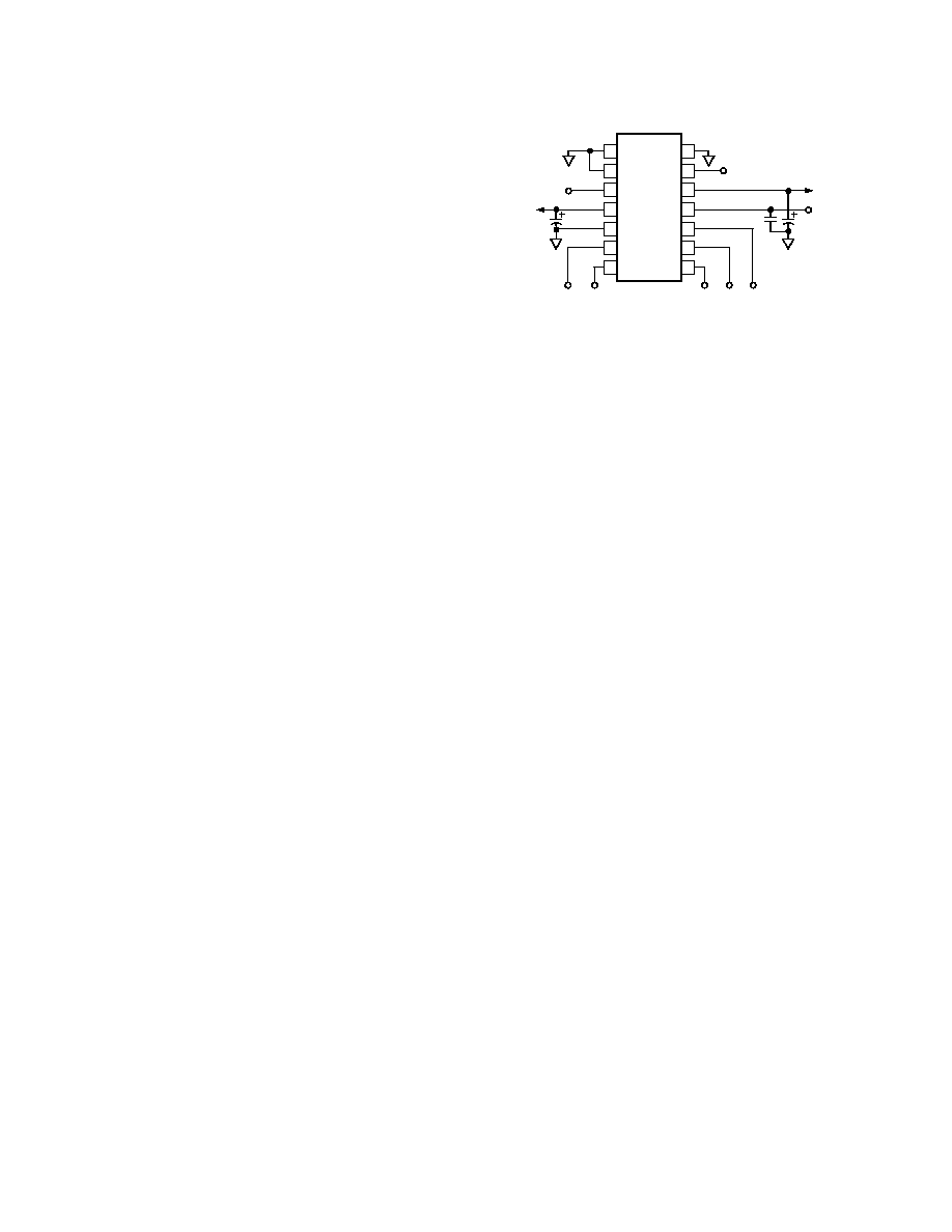
PIN CONFIGURATION
24
23
22
21
20
19
18
17
16
15
14
13
37
38
39
40
41
42
43
44
45
46
47
48
1
2
3
4
5
6
7
8
9
10 11 12
36 35 34 33 32
27 26 25
31 30 29 28
PIN 1
IDENTIFIER
TOP VIEW
(Not to Scale)
AD9801
VRT
VRB
SUBST
ADVSS
ADVSS
ADVDD
ADVDD
ADVSS
MODE1
MODE2
INT_BIAS2
CMLEVEL
DRVSS
DSUBST
DVSS
ADCCLK
INT_BIAS1
DVDD
STBY
PBLK
CLPOB
SHP
SHD
CLPDM
DVSS
ACVDD
ACVDD
ACVDD
CLAMP_BIAS
ACVSS
PGACONT2
PGACONT1
CCDBYP1
PIN
DIN
CCDBYP2
ADVSS
(LSB) D0
D1
D2
D3
D4
D5
D6
D7
D8
(MSB) D9
DRVDD
AD9801
5
REV. 0
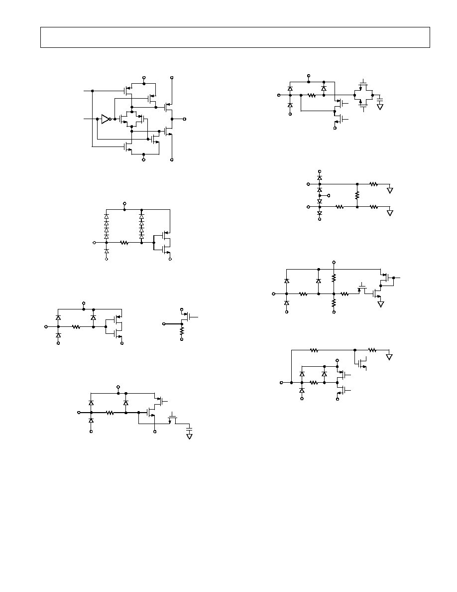
EQUIVALENT INPUT CIRCUITS
DVDD
DRVDD
DVSS
DRVSS
Figure 1. Pins 211 (DB0DB9)
DVDD
DSUBST
DVSS
200
Figure 2. Pin 21 (SHP) and Pin 22 (SHD)
DVDD
DSUBST
DVSS
200
ADVDD
ADVSS
9.3k
Figure 3. Pin 16 (ADCCLK) Figure 4. Pin 37 (CMLEVEL)
ACVDD
SUBST
DVSS
200
Figure 5. Pin 25 (CCDBYP2) and Pin 28 (CCDBYP1)
ACVDD
SUBST
ACVSS
50
10pF
Figure 6. Pin 26 (DIN) and Pin 27 (PIN)
ACVDD
SUBST
ACVDD
1k
8k
8k
10k
PGACONT1
PGACONT2
Figure 7. Pin 29 (PGACONT1) and Pin 30 (PGACONT2)
ACVSS
SUBST
ACVSS
5.25k
10k
30k
50
Figure 8. Pin 32 (CLAMP BIAS)
ACVDD
SUBST
ADVSS
Figure 9. Pin 48 (VRT) and Pin 47 (VRB)
AD9801
6
REV. 0
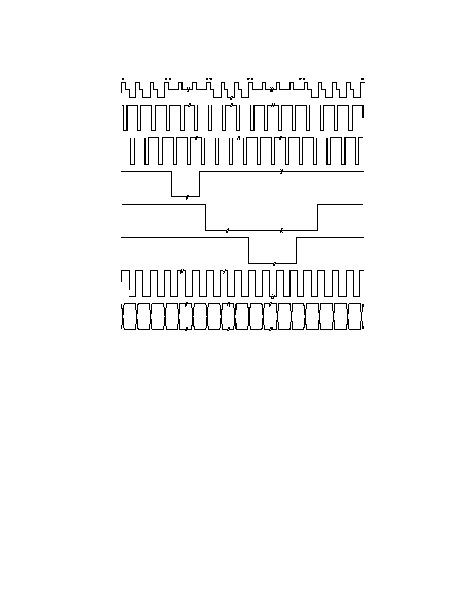
EFFECTIVE
PIXEL
INTERVAL
BLACK
LEVEL
INTERVAL
BLANKING
INTERVAL
DUMMY
BLACK
INTERVAL
EFFECTIVE
PIXEL
INTERVAL
CCD
SHP
SHD
CLPOB
PBLK
CLPDM
ADCCLK
ADC DATA
NOTE:
CLPDM OVERWRITES PBLK
CLAMP TIMING NEEDS TO BE ADJUSTED RELATIVE TO CCD'S BLACK PIXELS
Figure 10. Typical Horizontal Interval Timing
AD9801
7
REV. 0
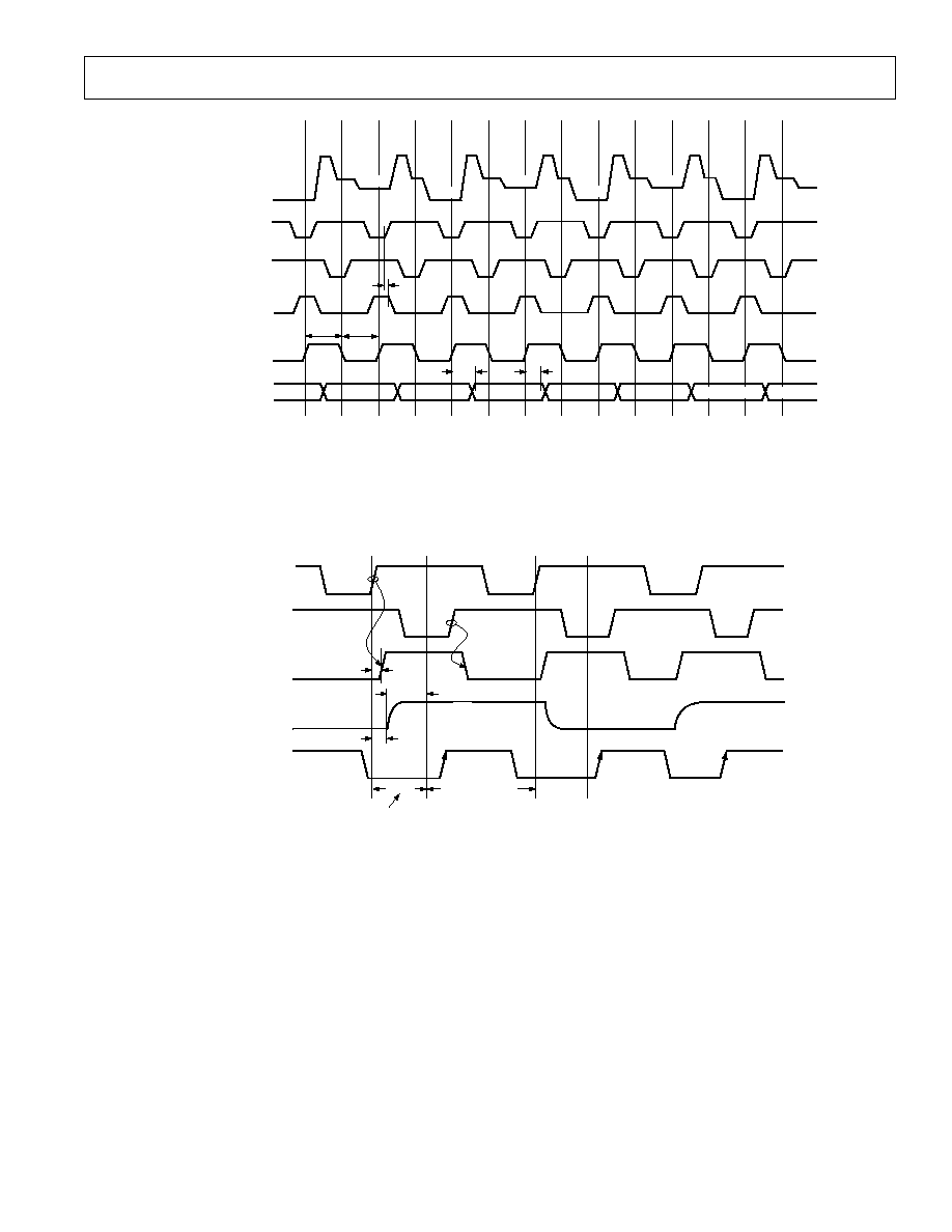
CCD SIGNAL
(DELAYED TO MATCH
ACTUAL SAMPLING
EDGE)
SHD
t
ID
35ns
35ns
t
OD
t
H
DATA N1
DATA N
N+1
N+2
N+3
N
N+4
1
2
3
4
5
6
7
SHP
ACTUAL
SAMPLING
EDGE
ADCCLK
DIGITAL OUT
OUTPUT LOAD C
L
= 20pF
OUTPUT DELAY
t
OD
= 15ns
LATENCY = 5 CYCLES
INTERNAL CLOCK DELAY
t
HD
= 3ns
HOLD TIME
t
H
= 2ns
Figure 11. Timing Diagram
SHP
15ns
SHD
ADCCLK
5ns
10ns
5ns
RISING EDGE
ANYWHERE IN
THIS PERIOD OK
INHIBITED PERIOD
FOR ADCCLK
TO CHANGE
PRE-ADC
OUTPUT LATCH
PRE-ADC
OUTPUT LATCH
DATA TRANSITION
Figure 12. ADCCLK Timing Edge
AD9801
8
REV. 0
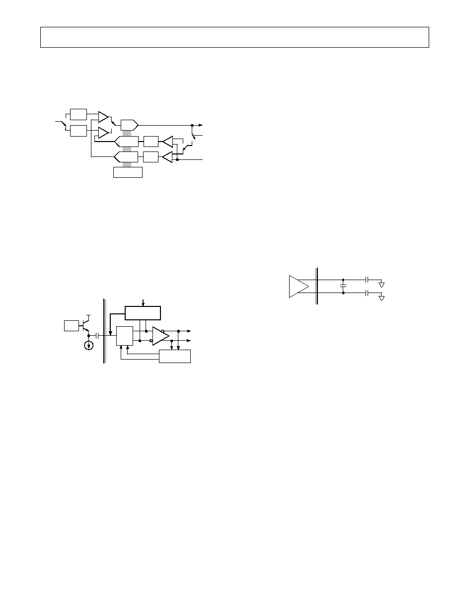
THEORY OF OPERATION
Introduction
The AD9801 is a 10-bit analog-to-digital interface for CCD
cameras. The block level diagram of the system is shown in
Figure 13. The device includes a correlated double sampler
(CDS), 0 dB31 dB variable gain amplifier (PGA), black level
correction loop, input clamp and voltage reference. The only
external analog circuitry required at the system level is an emitter
follower buffer between the CCD output and AD9801 inputs.
CLAMP
CDS
BLACK
LEVEL
PGA
10b
ADC
REF
OUT
GAIN
IN
Figure 13.
Correlated Double Sampling (CDS)
CDS is important in high performance CCD systems as a
method for removing several types of noise. Basically, two
samples of the CCD output are taken: one with the signal
present ("data") and one without ("reference"). Subtracting
these two samples removes any noise that is common--or
correlated--to both.
Figure 14 shows the block diagram of the AD9801's CDS. The
S/H blocks are directly driven by the input and the sampling
function is performed passively, without the use of amplifiers.
10pF
Q1
S/H
Q2
S/H
S
OUT
FROM
CCD
Figure 14.
This implementation relies on the off-chip emitter follower
buffer to drive the two 10 pF sampling capacitors. Only one
capacitor at a time is seen at the input pin.
The AD9801 actually uses two CDS circuits in a "ping pong"
fashion to allow the system more acquisition time. In this way,
the output from one of the two CDS blocks will be valid for an
entire clock cycle. Thus, the bandwidth requirement of the
subsequent gain stage is reduced as compared to that for a single
CDS channel system. This lower bandwidth translates to lower
power and noise.
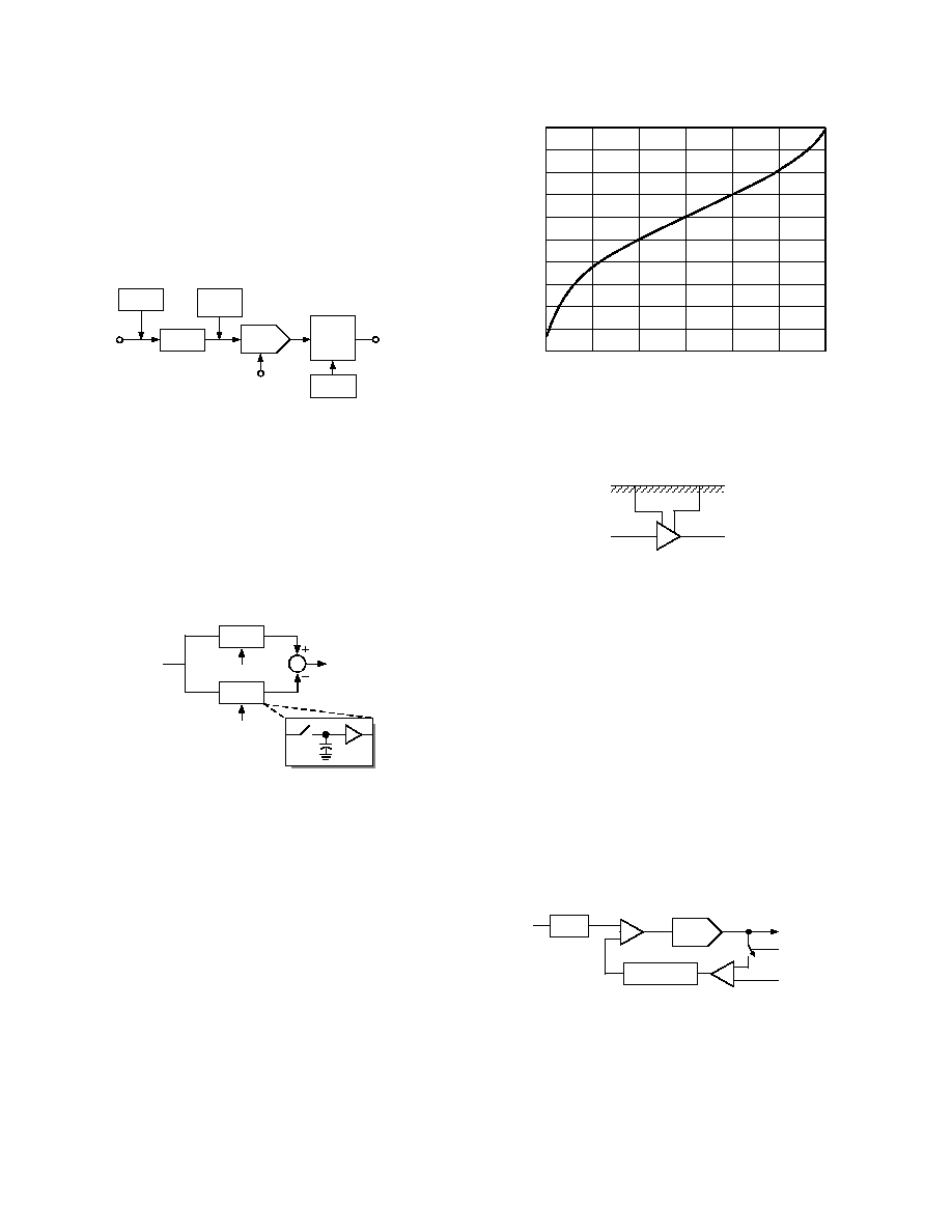
Programmable Gain Amplifier (PGA)
The on-chip PGA provides a (linear in dB) gain range of
0 dB31.5 dB. A typical gain characteristic plot is shown in
Figure 15. Only the range from 0.3 V to 2.7 V is intended for
actual use.
GAIN dB
PGACONT1 Volts
35
15
0
3
0.5
1
1.5
2
2.5
30
15
0
5
10
25
20
10
5
Figure 15.
As shown in Figure 16, PGA control is provided through the
PGACONT1 and PGACONT2 inputs. PGACONT1 provides
coarse and PGACONT2 fine (1/16) gain control.
A
PGACONT1
PGACONT2
PGACONT1 = COURSE CONTROL
PGACONT2 = FINE CONTROL (1/16)
Figure 16.
Black Level Clamping
For correct processing, the CCD signal must be referenced to a
well established "black level" by the AD9801. At the edge of the
CCD, there is a collection of pixels that are covered with metal
to prevent any light penetration. As the CCD is read out, these
"black pixels" provide a calibration signal that is used to
establish the black level.
The feedback loop shown in Figure 17 is closed around the
PGA during the calibration interval (CLPOB = LOW) to set the
black level. As the black pixels are being processed, an integrator
block measures the difference between the input level and the
desired reference level. This difference, or error, signal is
amplified and passed to the CDS block where it is added to the
incoming pixel data. As a result of this process, the black pixels
are digitized at one end of the ADC range, taking maximum
advantage of the available linear range of the system.
PGA
ADC
IN
CLPOB
NEG REF
INTEGRATOR
CDS
Figure 17.
AD9801
9
REV. 0
The actual implementation of this loop is slightly more compli-
cated as shown in Figure 18. Because there are two separate
CDS blocks, two black level feedback loops are required and
two offset voltages are developed. Figure 18 also shows an
additional PGA block in the feedback loop labeled "RPGA."
PGA
ADC
IN
CLPOB
NEG REF
CONTROL
CDS1
RPGA2
INT2
CDS1
RPGA1
INT1
Figure 18.
The RPGA uses the same control inputs as the PGA, but has
the inverse gain. The RPGA functions to attenuate by the same
factor as the PGA amplifies, keeping the gain and bandwidth of
the loop constant.
Input Bias Level Clamping
The buffered CCD output is connected to the AD9801 through
an external coupling capacitor. The dc bias point for this coupling
capacitor is established during the clamping (CLPDM = LOW)
period using the "dummy clamp" loop shown in Figure 19.
When closed around the CDS, this loop establishes the desired
DC bias point on the coupling capacitor.
BLACK
LEVEL CLP
CCD
INPUT
CLAMP
CDS
CLPDM
TO ADC
PGA
Figure 19.
Input Blanking
In some applications, the AD9801's input may be exposed to
large signals from the CCD. These signals can be very large,
relative to the AD9801's input range, and could thus saturate
on-chip circuit blocks. Recovery time from such saturation
conditions could be substantial.
To avoid problems associated with processing these transients,
the AD9801 includes an input blanking function. When active
(PBLK = LOW), this function stops the CDS operation and
allows the user to disconnect the CDS inputs from the CCD
buffer.
If the input voltage exceeds the supply rail by more than
0.3 V, protection diodes will be turned on, increasing current
flow into the AD9801 (see Equivalent Input Circuits). Such
voltage levels should be externally clamped to prevent device
damage or reliability degradation.
10-Bit Analog-to-Digital Converter (ADC)
The ADC employs a multibit pipelined architecture, which is
well-suited for high throughput rates while being both area and
power efficient. The multistep pipeline presents a low input
capacitance resulting in lower on-chip drive requirements. A
fully differential implementation was used to overcome head-
room constraints of the single +3 V power supply.
Differential Reference
The AD9801 includes a 0.5 V reference based on a differential,
continuous-time bandgap cell. Use of an external bypass
capacitor reduces the reference drive requirements, thus
lowering the power dissipation. The differential architecture was
chosen for its ability to reject supply and substrate noise.
Recommended decoupling shown in Figure 20.
VRT
REF
VRB
1µF
0.1µF
0.1µF
Figure 20.
Internal Timing
The AD9801's on-chip timing circuitry generates all clocks
necessary for operation of the CDS and ADC blocks. The user
needs only to synchronize the SHP and SHD clocks with the
CCD waveform, as all other timing is handled internally. The
ADCCLK signal is used to strobe the output data, and can be
adjusted to accommodate desired timing.
AD9801
10
REV. 0
APPLICATION INFORMATION
Generating Clock Signals
For best performance, the AD9801 should be driven by 3 V
logic levels. As shown in the Equivalent Input Circuits, the use
of 5 V logic for ADCCLK will turn on the protection diode to
DVDD, increasing the current flow into this pin. As a result,
noise and power dissipation will increase. The CDS clock inputs,
SHP and SHD, have additional protection and can withstand
direct 5 V levels.
External clamping diodes or resistor dividers can be used to
translate 5 V levels to 3 V levels, but the lowest power dissipa-
tion is achieved with a logic transceiver chip. National Semi-
conductor's 74LVX4245 provides a 5 V to 3 V level shift for up
to eight clock signals, and features a three-state option and low
power consumption. Philips Semiconductor and Quality also
manufacture similar devices.
Digitally Programmable Gain Control
The AD9801's PGA is controlled by an analog input voltage of
0.3 V to 2.7 V. In some applications, digital gain control is
preferable. Figure 21 shows a circuit using Analog Devices'
AD8402 Digital Potentiometer to generate the PGA control
voltage. The AD8402 functions as two individual potentiom-
eters, with a serial digital interface to program the position of
each wiper over 256 positions. The device will operate with 3 V
or 5 V supplies, and features a power-down mode and a reset
function.
To keep external components to a minimum, the ends of the
"potentiometers" can be tied to ground and +3 V. One pot is
used for the coarse gain adjust, PGACONT1, with steps of
about 0.2 dB/LSB. The other pot is used for fine gain control,
PGACONT2, and is capable of around 0.01 dB steps if all
eight bits are used. The two outputs should be filtered with 1
µ
F
or larger capacitors to minimize noise into the PGACONT pins
of the AD9801.
The disadvantage of this circuit is that the control voltage
will be supply dependent. If additional precision is required,
an external op amp can be used to amplify the VREFT (1.75 V)
or VREFB (1.25 V) pins on the AD9801 to the desired voltage
level. These reference voltages are stable over the operating
supply range of the AD9801. Low power, low cost, rail-to-rail
output amplifiers such as the AD820, OP150 and OP196 are
specified for 3 V operation. Alternatively, a precision voltage
1
2
3
4
7
6
5
AD8402-10
14
13
12
11
10
9
8
+3V
+3V
CS
SDI CLK
SHDN
RS
1µF
PGACONT2
1µF
0.1µF
+3V
PGACONT1
Figure 21. Digital Control of PGA
reference may be used. The REF193 from Analog Devices
features low power, low dropout performance, maintaining a
3 V output with a minimum 3.1 V supply when lightly loaded.
Power and Grounding Recommendations
The AD9801 should be treated as an analog component when
used in a system. The same power supply and ground plane
should be used for all of the pins. In a two-ground system, this
requires that the digital supply pins be decoupled to the analog
ground plane and the digital ground pins be connected to
analog ground for best noise performance. If any pins on the
AD9801 are connected to the system digital ground, noise can
capacitively couple inside the AD9801 (through package and die
parasitics) from the digital circuitry to the analog circuitry.
Separate digital supplies can be used, particularly if slightly
different driver supplies are needed, but the digital power pins
should still be decoupled to the same point as the digital ground
pins (analog ground plane). If the AD9801 digital outputs need
to drive a bus or substantial load, a buffer should be used at the
AD9801's outputs, with the buffer referenced to system digital
ground. In some cases, when system digital noise is not
substantial, it is acceptable to split the ground pins on the
AD9801 to separate analog and digital ground planes. If this is
done, be sure to connect the ground pins together at the
AD9801.
To further improve performance, isolating the driver supply
DRVDD from DVDD with a ferrite bead can help reduce
kickback effects during major code transitions. Alternatively,
the use of damping resistors on the digital outputs will reduce
the output risetimes, reducing the kickback effect.
AD9801
11
REV. 0
AVSS
6
7
4
3
2
U6
AD707
C50
0.1µF
C55
0.01µF
C56
0.1µF
C49
0.01µF
R14
68
C37
0.1µF
AVCC
CW
R6
10k
TP25
C70
10µF
16V
PGACONT1
AVCC
24
23
22
21
20
19
18
17
16
15
14
13
36 35 34 33 32
27 26 25
31 30 29 28
37
38
39
40
41
42
43
44
45
46
47
48
1
2
3
4
5
6
7
8
9
10 11 12
U1
AD9801
ADVSS
DRVDD
D0 (LSB)
D1
D2
D3
D4
D5
D6
D7
D8
D9 (MSB)
DRVSS
DVSS
CLPDM
SHD
SHP
CLPOB
PBLK
STBY
DVDD
ADCCLK
DVSS
DSUBST
VRT
VRB
SUBST
ADVSS
ADVDD
ADVDD
ADVSS
CLAMP_BIAS
MODE1
MODE2
INT_BIAS2
CMLEVEL
ADVSS
ACVDD
ACVDD
ACVDD
ACVSS
PGACONT2
PGACONT1
CCDBYP1
PIN
DIN
CCDBYP2
C14
0.1µF
C28
0.01µF
VDD
D0
D1
D2
D3
D4
D5
D6
D7
D8
D9
C5
0.1µF
C6
0.1µF
C2
0.1µF
C1
1µF
C3
0.1µF
C4
0.1µF
VDD
C8
0.1µF
C23
0.1µF
PIN
C10
2µF
C9
2µF
C12
0.1µF
C7
0.1µF
C61
0.1µF
PGACONT1
PGACONT2
VDD
TP5
PBLK
CLPOB
STBY
SHP
SHD
CLPDM
ADCCLK
C13
0.1µF
C29
0.01µF
VDD
DIN
0.1µF
VDD
CW
1k
JP3
JP2
JP1
JP4
FB4
C11
0.1µF
C46
0.1µF
C47
22µF
FB1
TP28
C66
0.1µF
VDD
+3V
JP1
C45
0.1µF
C44
22µF
FB2
TP27
C67
0.1µF
+5V
JP2
AVCC
INT_BIAS1
C40
0.1µF
C41
22µF
FB3
TP26
C68
0.1µF
AVSS
5V
JP3
TP29
GND
JP5
AVCC
AVSS
6
7
4
3
2
U7
AD707
C51
0.1µF
C57
0.01µF
C52
0.1µF
C54
0.01µF
R15
68
C36
0.1µF
AVCC
CW
R7
10k
TP24
C71
10µF
16V
PGACONT2
2
4
6
8
10
12
14
16
18
20
22
24
26
28
30
32
34
36
38
40
1
3
5
7
9
11
13
15
17
19
21
23
25
27
29
31
33
35
37
39
40 PIN HEADER
D9 (MSB)
D8
D7
D6
D5
D4
D3
D2
D1
D0 (LSB)
ADCCLK
Figure 22. AD9801EB Schematic
EVALUATION BOARD
Figure 22 shows the schematic for the AD9801 evaluation
board. Notice the use of a common ground and supply for the
AD9801, and the extensive supply and reference decoupling.
AD9801
12
REV. 0
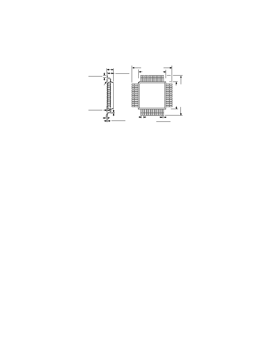
OUTLINE DIMENSIONS
Dimensions shown in inches and (mm).
C2975121/97
PRINTED IN U.S.A.
48-Terminal Plastic Thin Quad Flatpack
(ST-48)
0.354 (9.00) BSC
0.276 (7.0) BSC
1
12
13
25
24
36
37
48
TOP VIEW
(PINS DOWN)
0.276 (7.0) BSC
0.354 (9.00) BSC
0.011 (0.27)
0.006 (0.17)
0.019 (0.5)
BSC
SEATING
PLANE
0.063 (1.60) MAX
0
°
MIN
0
°
7
°
0.006 (0.15)
0.002 (0.05)
0.030 (0.75)
0.018 (0.45)
0.057 (1.45)
0.053 (1.35)
0.030 (0.75)
0.018 (0.45)
0.007 (0.18)
0.004 (0.09)