 | –≠–Ľ–Ķ–ļ—ā—Ä–ĺ–Ĺ–Ĺ—č–Ļ –ļ–ĺ–ľ–Ņ–ĺ–Ĺ–Ķ–Ĺ—ā: AD9698 | –°–ļ–į—á–į—ā—Ć:  PDF PDF  ZIP ZIP |

REV. B
Information furnished by Analog Devices is believed to be accurate and
reliable. However, no responsibility is assumed by Analog Devices for its
use, nor for any infringements of patents or other rights of third parties
which may result from its use. No license is granted by implication or
otherwise under any patent or patent rights of Analog Devices.
a
Ultrafast
TTL Comparators
AD9696/AD9698
FEATURES
4.5 ns Propagation Delay
200 ps Maximum Propagation Delay Dispersion
Single +5 V or 5 V Supply Operation
Complementary Matched TTL Outputs
APPLICATIONS
High Speed Line Receivers
Peak Detectors
Window Comparators
High Speed Triggers
Ultrafast Pulse Width Discriminators
Both devices allow the use of either a single +5 V supply or
Ī
5 V supplies. The choice of supplies determines the common
mode input voltage range available: ≠2.2 V to +3.7 V for
Ī
5 V
operation, +1.4 V to +3.7 V for single +5 V supply operation.
The differential input stage features high precision, with offset
voltages that are less than 2 mV and offset currents less than
1
Ķ
A. A latch enable input is provided to allow operation in ei-
ther sample-and-hold or track-and-hold applications.
The AD9696 and AD9698 are both available as commercial
temperature range devices operating from ambient temperatures
of 0
į
C to +70
į
C, and as extended temperature range devices for
ambient temperatures from ≠55
į
C to +125
į
C. Both versions are
available qualified to MIL-STD-883 class B.
Package options for the AD9696 include a 10-pin TO-100 metal
can, an 8-pin ceramic DIP, an 8-pin plastic DIP, and an 8-lead
small outline plastic package. The AD9698 is available in a
16-pin ceramic DIP, a 16-lead ceramic gullwing, a 16-pin plastic
DIP and a 16-lead small outline plastic package. Military quali-
fied versions of the AD9696 come in the TO-100 can and
ceramic DIP; the dual AD9698 comes in ceramic DIP.
GENERAL DESCRIPTION
The AD9696 and AD9698 are ultrafast TTL-compatible volt-
age comparators able to achieve propagation delays previously
possible only in high performance ECL devices. The AD9696 is
a single comparator providing 4.5 ns propagation delay, 200 ps
maximum delay dispersion and 1.7 ns setup time. The AD9698
is a dual comparator with equally high performance; both de-
vices are ideal for critical timing circuits in such applications as
ATE, communications receivers and test instruments.
FUNCTIONAL BLOCK DIAGRAM
AD9696/AD9698 Architecture
AD9698
#1
OUTPUT
INPUT
LATCH
GAIN
LEVEL
SHIFT
AD9696
NONINVERTING
INPUT
INVERTING
INPUT
LATCH
ENABLE
Q OUTPUT
Q OUTPUT
NONINVERTING
INPUT
INVERTING
INPUT
LATCH
ENABLE
Q OUTPUT
Q OUTPUT
#2
NONINVERTING
INPUT
INVERTING
INPUT
LATCH
ENABLE
Q OUTPUT
Q OUTPUT
One Technology Way, P.O. Box 9106, Norwood, MA 02062-9106, U.S.A.
Tel: 617/329-4700
World Wide Web Site: http://www.analog.com
Fax: 617/326-8703
© Analog Devices, Inc., 1997

REV. B
≠2≠
AD9696/AD9698≠SPECIFICATIONS
ABSOLUTE MAXIMUM RATINGS
1
Supply Voltage (+V
S
/≠V
S
) . . . . . . . . . . . . . . . . . . . . +7 V/≠7 V
Input Voltage Range . . . . . . . . . . . . . . . . . . . . . . . . . . . .
Ī
5 V
Differential Input Voltage . . . . . . . . . . . . . . . . . . . . . . . 5.4 V
Latch Enable Voltage . . . . . . . . . . . . . . . . . . . . . ≠0.5 V to +V
S
Output Current (Continuous) . . . . . . . . . . . . . . . . . . . 20 mA
Power Dissipation . . . . . . . . . . . . . . . . . . . . . . . . . . . 600 mW
Operating Temperature Range
2
AD9696/AD9698KN/KQ/KR . . . . . . . . . . . . 0
į
C to +70
į
C
AD9696/AD9698TQ . . . . . . . . . . . . . . . . ≠55
į
C to +125
į
C
Storage Temperature Range . . . . . . . . . . . . ≠65
į
C to +150
į
C
Junction Temperature
KQ/TQ Suffixes . . . . . . . . . . . . . . . . . . . . . . . . . . . +175
į
C
KN/KR Suffixes . . . . . . . . . . . . . . . . . . . . . . . . . . . +150
į
C
Lead Soldering Temperature (10 sec) . . . . . . . . . . . . +300
į
C
ELECTRICAL CHARACTERISTICS
(Supply Voltages = ≠5.2 V and +5.0 V; load as specified in Note 4,
unless otherwise noted)
0 C to +70 C
≠55 C to +125 C
AD9696/AD9698
AD9696/AD9698
Test
KN/KQ/KR
TQ
Parameter
Temp
Level
Min
Typ
Max
Min
Typ
Max
Units
INPUT CHARACTERISTICS
Input Offset Voltage
4
+25
į
C
I
1.0
2.0
1.0
2.0
mV
Full
VI
3.0
3.0
mV
Input Offset Voltage Drift
Full
V
10
10
Ķ
V/
į
C
Input Bias Current
+25
į
C
I
16
55
16
55
Ķ
A
Full
VI
110
110
Ķ
A
Input Offset Current
+25
į
C
I
0.4
1.0
0.4
1.0
Ķ
A
Full
VI
1.3
1.3
Ķ
A
Input Capacitance
+25
į
C
V
3
3
pF
Input Voltage Range
Ī
5.0 V
Full
VI
≠2.2
+3.7
≠2.2
+3 7
V
+5.0 V
Full
VI
+1.4
+3.7
+1.4
+3.7
V
Common Mode Rejection Ratio
Ī
5.0 V
Full
VI
80
85
80
85
dB
+5.0 V
Full
VI
57
63
57
63
dB
LATCH ENABLE INPUT
Logic "1" Voltage Threshold
Full
VI
2.0
2.0
V
Logic "0" Voltage Threshold
Full
VI
0.8
0.8
V
Logic "1" Current
Full
VI
10
10
Ķ
A
Logic "0" Current
Full
VI
1
1
Ķ
A
DIGITAL OUTPUTS
Logic "1" Voltage (Source 4 mA)
Full
VI
2.7
3.5
2.7
3.5
V
Logic "0" Voltage (Sink 10 mA)
Full
VI
0.4
0.5
0.4
0.5
V
SWITCHING PERFORMANCE
Propagation Delay (t
PD
)
5
Input to Output HIGH
Full
IV
4.5
7.0
4.5
7.0
ns
Input to Output LOW
Full
IV
4.5
7.0
4.5
7.0
ns
Latch Enable to Output HIGH
+25
į
C
IV
6.5
8.5
6.5
8.5
ns
Latch Enable to Output LOW
+25
į
C
IV
6.5
8.5
6.5
8.5
ns
Delta Delay Between Outputs
+25
į
C
IV
0.5
1.5
0.5
1.5
ns
Propagation Delay Dispersion
20 mV to 100 mV Overdrive
+25
į
C
V
100
100
ps
100 mV to 1.0 V Overdrive
+25
į
C
IV
100
200
100
200
ps
Rise Time
10
+25
į
C
V
1.85
1.85
ns
Fall Time
10
+25
į
C
V
1.35
1.35
ns
Latch Enable
Pulse Width [t
PW(E)
]
+25
į
C
IV
3.5
2.5
3.5
2.5
ns
Setup Time (t
S
)
+25
į
C
IV
3
1.7
3
1.7
ns
Hold Time (t
H
)
+25
į
C
IV
3
1.9
3
1.9
ns

0 C to +70 C
≠55 C to +125 C
AD9696/AD9698
AD9696/AD9698
Test
KN/KQ/KR
TQ
Parameter
Temp
Level
Min
Typ
Max
Min
Typ
Max
Units
POWER SUPPLY
6
Positive Supply Current
7
(+5.0 V)
AD9696
Full
VI
26
32
26
32
mA
AD9698
Full
VI
52
64
52
64
mA
Negative Supply Current
8
(≠5.2 V)
AD9696
Full
VI
2.5
4.0
2.5
4.0
mA
AD9698
Full
VI
5.0
8.0
5.0
8.0
mA
Power Dissipation
AD9696 +5.0 V
Full
V
130
130
mW
AD9696
Ī
5.0 V
Full
V
146
146
mW
AD9698 +5.0 V
Full
V
260
260
mW
AD9698
Ī
5.0 V
Full
V
292
292
mW
Power Supply Rejection Ratio
9
+25
į
C
VI
70
70
dB
Full
VI
65
65
dB
NOTES
1
Absolute maximum ratings are limiting values, to be applied individually,
and beyond which the serviceability of the circuit may be impaired. Functional
operability is not necessarily implied. Exposure to absolute maximum rating
conditions for an extended period of time may affect device reliability.
2
Typical thermal impedances:
AD9696 Metal Can
JA
= 170
į
C/W
JC
= 50
į
C/W
AD9696 Ceramic DIP
JA
= 110
į
C/W
JC
= 20
į
C/W
AD9696 Plastic DIP
JA
= 160
į
C/W
JC
= 30
į
C/W
AD9696 Plastic SOIC
JA
= 180
į
C/W
JC
= 30
į
C/W
AD9698 Ceramic DIP
JA
= 90
į
C/W
JC
= 25
į
C/W
AD9698 Plastic DIP
JA
= 100
į
C/W
JC
= 20
į
C/W
AD9698 Plastic SOIC
JA
= 120
į
C/W
JC
= 20
į
C/W
3
Load circuit has 420
from +V
S
to output; 460
from output to ground.
4
R
S
100
.
5
Propagation delays measured with 100 mV pulse; 10 mV overdrive.
6
Supply voltages should remain stable within
Ī
5% for normal operation.
7
Specification applies to both +5 V and
Ī
5 V supply operation.
8
Specification applies to only
Ī
5 V supply operation.
9
Measured with nominal values
Ī
5% of +V
S
and ≠V
S
.
10
Although fall time is faster than rise time, the complementary outputs cross at
midpoint of logic swing because of delay on start of falling edge.
Specifications subject to change without notice.
EXPLANATION OF TEST LEVELS
Test Level
I
≠ 100% production tested.
II
≠ 100% production tested at +25
į
C, and sample tested at
specified temperatures.
III
≠ Sample tested only.
IV
≠ Parameter is guaranteed by design and characterization
testing.
V
≠ Parameter is a typical value only.
VI
≠ All devices are 100% production tested at +25
į
C.
100% production tested at temperature extremes for
extended temperature devices; sample tested at temp-
erature extremes for commercial/industrial devices.
ORDERING GUIDE
Package
Model
Package
Temperature
Option
1
AD9696KN
Plastic DIP
0
į
C to +70
į
C
N-8
AD9696KR
SOIC
0
į
C to +70
į
C
R-8
AD9696KQ
Cerdip
0
į
C to +70
į
C
Q-8
AD9696TQ
Cerdip
≠55
į
C to +125
į
C Q-8
AD9696TZ/883B
2
Gullwing
≠55
į
C to +125
į
C Z-8A
AD9698KN
Plastic DIP
0
į
C to +70
į
C
N-16
AD9698KR
SOIC
0
į
C to +70
į
C
R-16A
AD9698KQ
Cerdip
0
į
C to +70
į
C
Q-16
AD9698TQ
Cerdip
≠55
į
C to +125
į
C Q-16
AD9698TZ/883B
3
Gullwing
≠55
į
C to +125
į
C Z-16
NOTES
1
N = Plastic DIP, Q = Cerdip, R = Small Outline (SOIC), Z = Ceramic Leaded
Chip Carrier.
2
Refer to AD9696TZ/883B military data sheet.
3
Refer to AD9698TZ/883B military data sheet.
AD9696/AD9698
≠3≠
REV. B

AD9696/AD9698
≠4≠
REV. B
PIN CONFIGURATIONS
AD9696KN/KR/KQ/TQ/TZ
Q1
OUT
(N/C)
Q1
OUT
(≠V
S
)
GROUND (≠IN
1
)
LATCH ENABLE 1 (+IN
1
)
N/C (+IN
2
)
≠V
S
(≠IN
2
)
≠IN
1
(+V
S
)
TOP VIEW
(Not to Scale)
1
2
3
4
5
6
7
8
9
10
11
12
13
14
16
15
+IN
1
(N/C)
+IN
2
(LATCH ENABLE 2)
≠IN
2
(GROUND)
N/C (Q2
OUT
)
LATCH ENABLE 2 (Q1
OUT
)
Q2
OUT
(GROUND)
Q2
OUT
(LATCH ENABLE 1)
AD9698KN/KQ/TQ
[AD9698KR/TZ PINOUTS SHOWN IN ( )]
GROUND (Q1
OUT
)
+V
S
(Q2
OUT
)
LATCH
ENABLE
1
2
3
4
TOP VIEW
(Not to Scale)
5
6
7
8
+V
S
+IN
≠IN
≠V
S
GROUND
Q
OUT
Q
OUT
Name
Function
Q1
OUT
One of two complementary outputs. Q1
OUT
will be at logic HIGH if voltage at +IN
1
is greater than voltage at
≠IN
1
and LATCH ENABLE 1 is at logic LOW.
Q1
OUT
One of two complementary outputs. Q1
OUT
will be at logic HIGH if voltage at ≠IN
1
is greater than voltage at
+IN
1
and LATCH ENABLE 1 is at logic LOW.
GROUND
Analog and digital ground return. All GROUND pins should be connected together and to a low impedance
ground plane near the comparator.
LATCH
Output at Q1
OUT
will track differential changes at the inputs when LATCH ENABLE 1 is at logic LOW.
ENABLE 1
When LATCH ENABLE 1 is at logic HIGH, the output at Q1
OUT
will reflect the input state at the application of
the latch command, delayed by the Latch Enable Setup Time (t
S
). Since the architecture of the input stage (see
block diagram) is faster than the logic of the latch stage, data will typically be latched if applied to the comparator(s)
within 1.7 ns after the latch. This is the Setup Time (t
S
); for guaranteed performance, t
S
must be 3 ns.
N/C
No internal connection to comparator.
≠V
S
Negative power supply connection; nominally ≠5.2 V.
≠IN
1
Inverting input of differential input stage for Comparator #1.
+IN
1
Noninverting input of differential input stage for Comparator #1.
+IN
2
Noninverting input of differential input stage for Comparator #2.
≠IN
2
Inverting input of differential input stage for Comparator #2.
+V
S
Positive power supply connection; nominally +5 V.
LATCH
Output at Q2
OUT
will track differential changes at the inputs when LATCH ENABLE 2 is at logic LOW.
ENABLE 2
When LATCH ENABLE 2 is at logic HIGH, the output at Q2
OUT
will reflect the input state at the application of
the latch command, delayed by the Latch Enable Setup Time (t
S
). Since the architecture of the input stage (see
block diagram) is faster than the logic of the latch stage, data will typically be latched if applied to the comparator(s)
within 1.7 ns after the latch. This is the Setup Time (t
S
); for guaranteed performance, t
S
must be 3 ns.
Q2
OUT
One of two complementary outputs. Q2
OUT
will be at logic HIGH if voltage at ≠IN
2
is greater than voltage at
+IN
2
and LATCH ENABLE 2 is at logic LOW.
Q2
OUT
One of two complementary outputs. Q2
OUT
will be at logic HIGH if voltage at +IN
2
is greater than voltage at
≠IN
2
and LATCH ENABLE 2 is at logic LOW.
WARNING!
ESD SENSITIVE DEVICE
CAUTION
ESD (electrostatic discharge) sensitive device. Electrostatic charges as high as 4000 V readily
accumulate on the human body and test equipment and can discharge without detection.
Although the AD9696/AD9698 features proprietary ESD protection circuitry, permanent dam-
age may occur on devices subjected to high energy electrostatic discharges. Therefore, proper
ESD precautions are recommended to avoid performance degradation or loss of functionality.

AD9696/AD9698
≠5≠
REV. B
t
H
50%
50%
LATCH
ENABLE
DIFFERENTIAL
INPUT VOLTAGE
Q
TWO DIODES
ABOVE GROUND
LATCH
COMPARE
Q
t
PD
t
PD (E)
V
OS
≠ MINIMUM SETUP TIME (Typically 1.7ns)
≠ MINIMUM HOLD TIME (Typically 1.9ns)
≠ INPUT TO OUTPUT DELAY
≠ LATCH ENABLE TO OUTPUT DELAY
t
H
t
S
t
PD
t
PD (E)
≠ MINIMUM LATCH ENABLE PULSE WIDTH (Typically 2.5ns)
≠ INPUT OFFSET VOLTAGE
≠ OVERDRIVE VOLTAGE
V
OS
V
OD
t
PW (E)
V
OD
V
IN
t
PW (E)
t
S
AD9696/AD9698 Timing Diagram
DIE LAYOUT AND MECHANICAL INFORMATION
Die Dimensions AD9696 . . . . . . . . . . . . . 59
◊
71
◊
15 (
Ī
2) mils
AD9698 . . . . . . . . . . . . 79
◊
109
◊
15 (
Ī
2) mils
Pad Dimensions . . . . . . . . . . . . . . . . . . . . . . . . . . . . . 4
◊
4 mils
Metalization . . . . . . . . . . . . . . . . . . . . . . . . . . . . . . Aluminum
Backing . . . . . . . . . . . . . . . . . . . . . . . . . . . . . . . . . . . . . None
Substrate Potential . . . . . . . . . . . . . . . . . . . . . . . . . . . . . . . ≠V
S
Passivation . . . . . . . . . . . . . . . . . . . . . . . . . . . . . . . . . . Nitride
THEORY OF OPERATION
Refer to the block diagram of the AD9696/AD9698 compara-
tors. The AD9696 and AD9698 TTL voltage comparator archi-
tecture consists of five basic stages: input, latch, gain, level shift
and output. Each stage is designed to provide optimal perfor-
mance and make it easy to use the comparators.
The input stage operates with either a single +5-volt supply, or
with a +5-volt supply and a ≠5.2-volt supply. For optimum
power efficiency, the remaining stages operate with only a single
+5-volt supply. The input stage is an input differential pair
without the customary emitter follower buffers. This configura-
tion increases input bias currents but maximizes the input volt-
age range.
A latch stage allows the most recent output state to be retained
as long as the latch input is held high. In this way, the input to
the comparator can be changed without any change in the out-
put state. As soon as the latch enable input is switched to LOW,
the output changes to the new value dictated by the signal ap-
plied to the input stage.
The gain stage assures that even with small values of input volt-
age, there will be sufficient levels applied to the following stages
to cause the output to switch TTL states as required. A level
shift stage between the gain stage and the TTL output stage
guarantees that appropriate voltage levels are applied from the
gain stage to the TTL output stage.
Only the output stage uses TTL logic levels; this minimum use
of TTL circuits maximizes speed and minimizes power con-
sumption. The outputs are clamped with Schottky diodes to as-
sure that the rising and falling edges of the output signal are
closely matched.
The AD9696 and AD9698 represent the state of the art in high
speed TTL voltage comparators. Great care has been taken to
optimize the propagation delay dispersion performance. This as-
sures that the output delays will remain constant despite varying
levels of input overdrive. This characteristic, along with closely
matched rising and falling outputs, provides extremely consis-
tent results at previously unattainable speeds.

AD9696/AD9698
≠6≠
REV. B
R
R
A2
A1
AD9698
+IN
1
≠IN
1
+V
REF
R
1
Q
1 OUT
R = 10k
R
1
+ R
2
>5k
A
1
,A
2
= AD708 or OP≠ 290
(Ī5V) (+5V)
R
2
Q
1 OUT
Q
1 OUT
Q
2 OUT
Q
2 OUT
+Q
2 OUT
≠V
REF
V
SIGNAL
V
IN
+IN
2
≠IN
2
Figure 1. AD9698 Used as Window Detector
When configured as shown, the op amps generate reference lev-
els for the comparators that are equally spaced above and below
the applied V
IN
. The width of the window is established by the
ratio of R1 and R2. For a given ratio of R1 and R2, +V
REF
and
≠V
REF
will be fixed percentages above and below V
IN
. As an ex-
ample, using 2.2 k
for R1 and 10 k
for R2 creates a
Ī
10%
window. When V
IN
equals +3 V, +V
REF
will be +3.3 V and
≠V
REF
will be +2.7 V. Likewise, for a ≠2 V input, the thresholds
will be ≠1.8 V and ≠2.2 V. Windows of differing percentage
width can be calculated with the equation:
(1≠X)/2X = R2/R1
where:
X = % window
Additionally, the low impedance of the op amp outputs assures
that the threshold voltages will remain constant when the input
currents change as the signal passes through the threshold volt-
age levels.
The output of the AND gate will be high while the signal is in-
side the window. Q1
OUT
will be high when the signal is above
+V
REF
, and Q2
OUT
will be high when the signal is below ≠V
REF
.
Crystal Oscillator
Oscillators are used in a wide variety of applications from audio
circuits to waveform generators, from ATE triggers and tele-
communications transceivers to radar. Figure 2 shows a versatile
and inexpensive oscillator. The circuit uses the AD9696, in a
positive feedback mode, and is capable of generating accurate
and stable oscillations with frequencies ranging from 1 MHz to
more than 40 MHz.
To generate oscillations from 1 to 25 MHz, a fundamental
mode crystal is used without the dc blocking capacitor and
choke. The parallel capacitor on the inverting input is selected
for stability (0.1
Ķ
F for 1≠10 MHz; 220 pF for frequencies
above 10 MHz).
APPLICATIONS
General
Two characteristics of the AD9696 and AD9698 should be con-
sidered for any application. First is the fact that all TTL com-
parators are prone to oscillate if the inputs are close to equal for
any appreciable period of time. One instance of this happening
would be slow changes in the unknown signal; the probability of
oscillation is reduced when the unknown signal passes through
the threshold at a high slew rate. Another instance is if the un-
known signal does not overdrive the comparator logic. Unless
they are overdriven, TTL comparators have undershoot when
switching logic states. The smaller the overdrive, the greater the
undershoot; when small enough, the comparator will oscillate,
not being able to determine a valid logic state. For the AD9696
and AD9698, 20 mV is the smallest overdrive which will assure
crisp switching of logic states without significant undershoot.
The second characteristic to keep in mind when designing
threshold circuits for these comparators is twofold: (1) bias cur-
rents change when the threshold is exceeded; and (2) ac input
impedance decreases when the comparator is in its linear region.
During the time both transistors in the differential pair are con-
ducting, the ac input impedance drops by orders of magnitude.
Additionally, the input bias current switches from one input to
the other, depending upon whether or not the threshold is ex-
ceeded. As a result, the input currents follow approximately the
characteristic curves shown below.
{
SIGNAL
VOLTAGE
AT +INPUT
+INPUT
CURRENT
≠ INPUT
CURRENT
LINEAR
REGION
Threshold Input Currents
This characteristic will not cause problems unless a high imped-
ance threshold circuit or drive circuit is employed. A circuit
similar to that shown in the window comparator application can
eliminate this possible problem.
Window Comparator
Many applications require determining when a signal's voltage
falls within, above, or below a particular voltage range. A simple
tracking window comparator can provide this data. Figure 1
shows such a window comparator featuring high speed, TTL
compatibility, and ease of implementation.
Two comparators are required to establish a "window" with up-
per and lower threshold voltages. The circuit shown uses the
AD9698 dual ultrafast TTL comparator. In addition to the cost
and space savings over a design using two single comparators,
the dual comparator on a single die produces better matching of
both dc and dynamic characteristics.

AD9696/AD9698
≠7≠
REV. B
2
AD9696
≠IN
+IN
+V
S
1≠ 40MHz
LATCH
ENABLE
+
≠
OSCILLATOR
OUTPUT
GROUND
Q
OUT
2k
+V
S
0.1ĶF
(220pF for Freq. > 10MHz)
0.1ĶF
FOR USE WITH
OVERTONE
CRYSTAL
(VALUE
DEPENDS
ON FREQ.)
3
1
5
7
8
4
6
2k
2k
Q
OUT
≠V
S
Figure 2. AD9696 Oscillator Circuit (Based on DIP Pinouts)
When generating frequencies using a nonfundamental mode
crystal, a choke and dc blocking capacitor are added. As an ex-
ample, a 36 MHz oscillator can be achieved by using a 12 MHz
crystal operating on its third overtone. To suppress oscillation at
the 12 MHz fundamental, the value of the choke is chosen to
provide a low reactive impedance at the fundamental frequency
while maintaining a high reactive impedance at the desired out-
put frequency (for 36 MHz operation, L = 1.8
Ķ
H). The shunt
capacitor at the inverting input has a value of 220 pF for a stable
36 MHz frequency.
LAYOUT CONSIDERATIONS
When working with high speed circuits, proper layout is critical.
Analog signal paths should be kept as short as possible and be
properly terminated to avoid reflections. In addition, digital sig-
nal paths should be kept short, and run lengths should be mat-
ched to avoid propagation delay mismatch. All analog signals
should be kept as far away from digital signal paths as possible;
this reduces the amount of digital switching noise that might be
capacitively coupled into the analog section of the circuit.
In high speed circuits, layout of the ground circuit is the most
important factor. A single, low impedance ground plane, on the
component side of the board, will reduce noise in the circuit
ground. It is especially important to maintain continuity of the
ground plane under and around the AD9696 or AD9698.
Sockets limit the dynamic performance of the device and should
be used only for prototypes or evaluation.
8
7
6
5
4
3
2
1
AD9696
(8-PIN DIP)
0.1ĶF
0.1ĶF
AD1
AD2
GND
RESISTORS ARE 1k
Ī5%
≠ V
S
+V
S
5Ķs
≠0.9V
AD1
AD2
≠0.9 V
≠1.7V
≠1.7V
Burn-In Circuit
AD9696/AD9698
≠8≠
REV. B
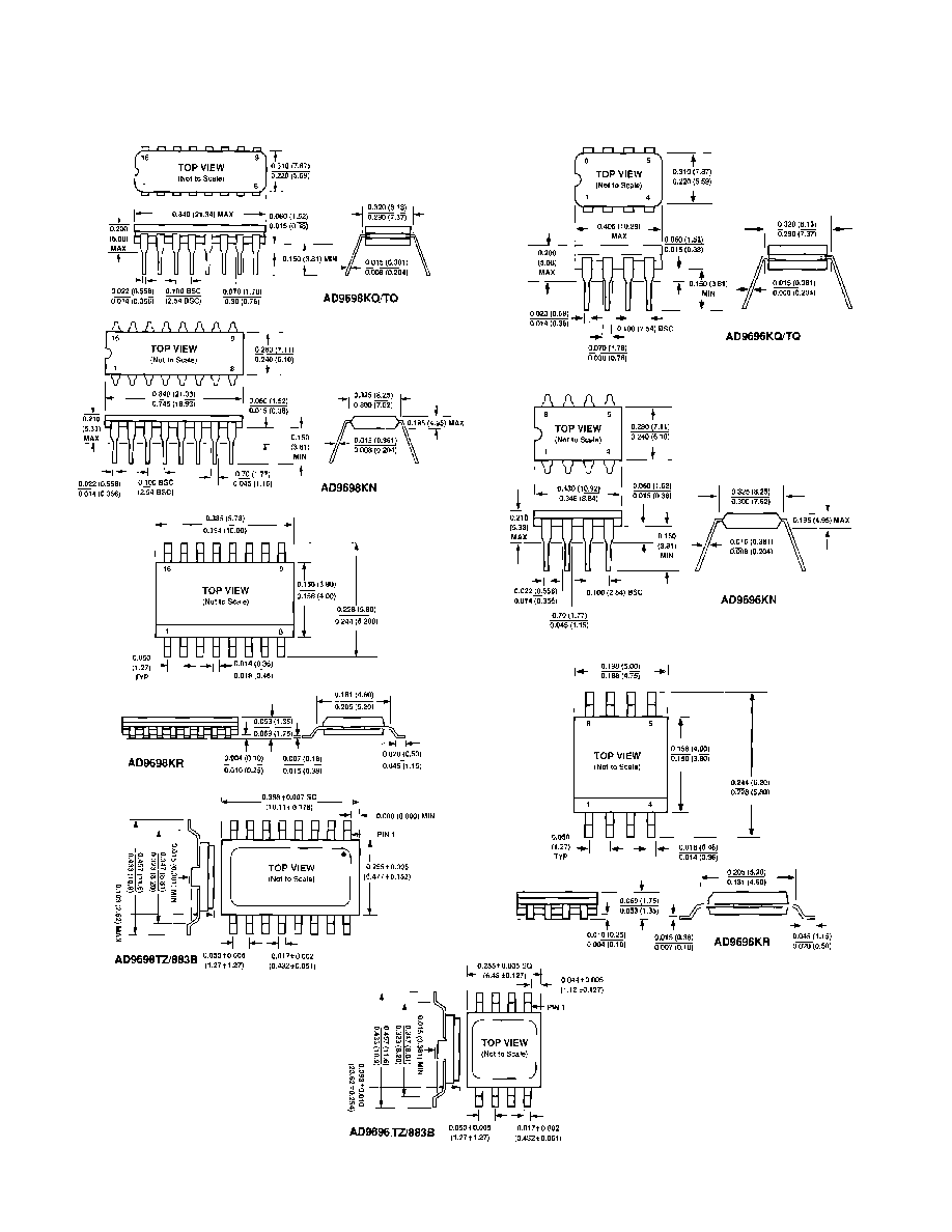
OUTLINE DIMENSIONS
Dimensions shown in inches and (mm).
C1320a≠10≠2/91
PRINTED IN U.S.A.