 | ÐлекÑÑоннÑй компоненÑ: AD9510 | СкаÑаÑÑ:  PDF PDF  ZIP ZIP |
AD9510 800 MHz Clock Distribution IC, PLL Core, Dividers, Delay Adjust, Eight Outputs Preliminary Data Sheet (Rev. PrA)
800 MHz Clock Distribution IC, PLL Core,
Dividers, Delay Adjust, Eight Outputs
Preliminary Technical Data
AD9510
Rev. PrA
Information furnished by Analog Devices is believed to be accurate and reliable.
However, no responsibility is assumed by Analog Devices for its use, nor for any
infringements of patents or other rights of third parties that may result from its use.
Specifications subject to change without notice. No license is granted by implication
or otherwise under any patent or patent rights of Analog Devices. Trademarks and
registered trademarks are the property of their respective owners.
One Technology Way, P.O. Box 9106, Norwood, MA 02062-9106, U.S.A.
Tel: 781.329.4700
www.analog.com
Fax: 781.326.8703
© 2004 Analog Devices, Inc. All rights reserved.
FEATURES
Low phase noise phase-locked loop core
Reference input frequencies to 250 MHz
Programmable dual-modulus prescaler
Programmable charge pump (CP) current
Separate CP supply (VCP) extends tuning range
Two 1.5 GHz, differential clock inputs
8 programmable dividers, 1 to 32, all integers
Phase select for output-to-output coarse delay adjust
4 independent 800 MHz LVPECL outputs
Additive output jitter 225 fs rms
4 independent 800 MHz/250 MHz LVDS/CMOS clock outputs
Additive output jitter 275 fs rms
Fine delay adjust on 2 outputs, 6-bit delay words
4-wire or 3-wire serial control port
Space-saving 64-lead LFCSP
APPLICATIONS
Low jitter, low phase noise clock distribution
Clocking high speed ADCs, DACs, DDS, DDC, DUC, MxFEs
High performance wireless transceivers
High performance instrumentation
Broadband infrastructure
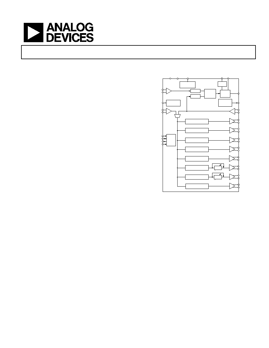
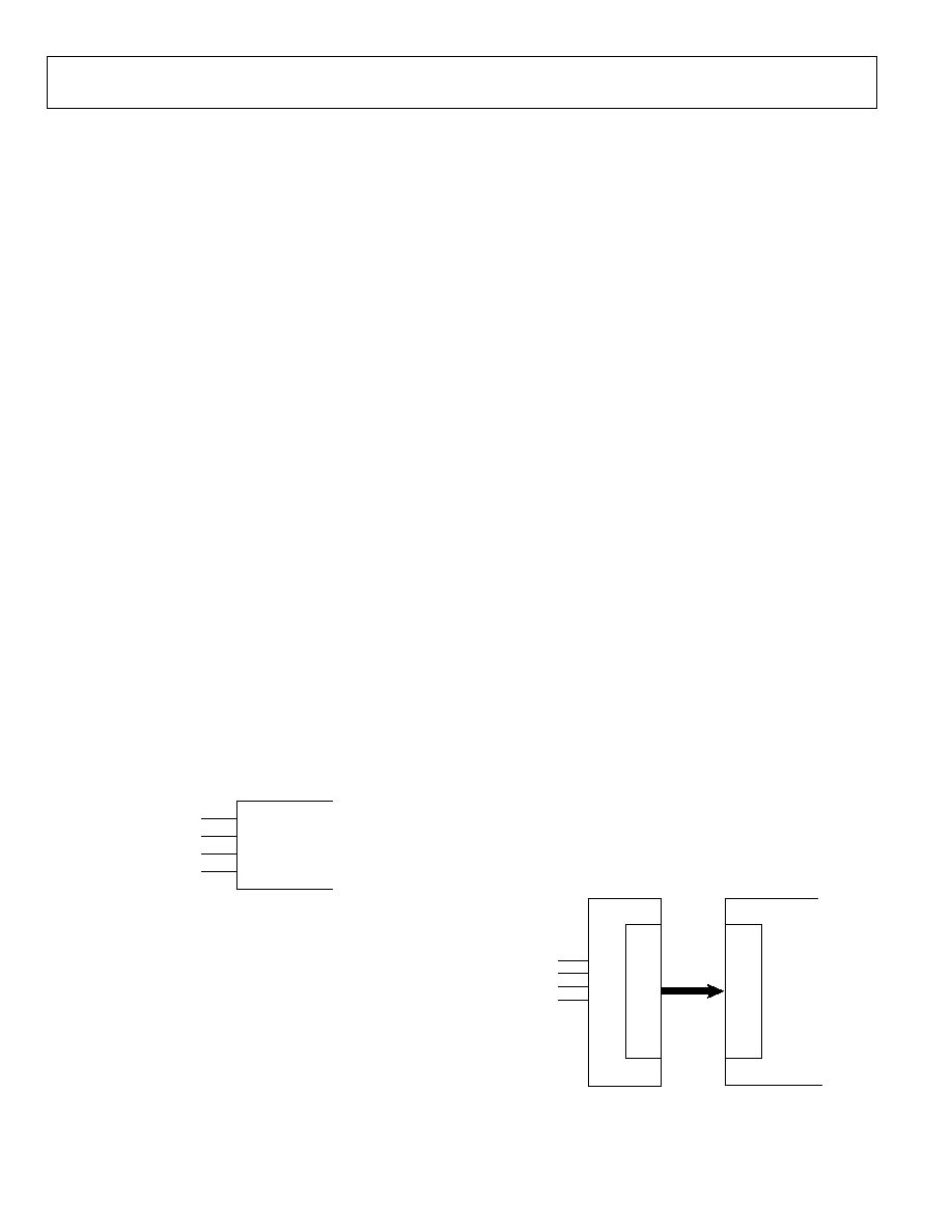
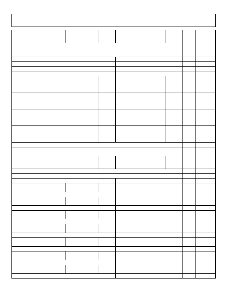
FUNCTIONAL BLOCK DIAGRAM
VS
GND
RSET
CPRSET VCP
CP
STATUS
CLK2
CLK2B
OUT0
OUT0B
OUT1
OUT1B
OUT2
OUT2B
OUT3
OUT3B
OUT4
OUT4B
OUT5
OUT5B
OUT6
OUT6B
OUT7
OUT7B
SCLK
SDIO
SDO
CSB
LVPECL
CHARGE
PUMP
PLL
REF
PHASE
FREQUENCY
DETECTOR
R DIVIDER
N DIVIDER
DISTRIBUTION
REF
SYNCB,
RESETB PDB
CLK1B
CLK1
FUNCTION
REFINB
REFIN
PLL
SETTINGS
AD9510
PROGRAMMABLE DIVIDERS
& PHASE ADJUST
/1,/2,/3 ... /31,/32
/1,/2,/3... /31,/32
/1,/2,/3 ... /31,/32
/1,/2,/3 ... /31,/32
/1,/2,/3... /31,/32
T
/1,/2,/3 ... /31,/32
/1,/2,/3... /31,/32
T
/1,/2,/3 ... /31,/32
LVDS/CMOS
PORT
CONTROL
SERIAL
LVPECL
LVPECL
LVPECL
LVDS/CMOS
LVDS/CMOS
LVDS/CMOS
Figure 1.
GENERAL DESCRIPTION
The AD9510 provides a multi-output clock distribution
function along with an on-chip PLL core. The design
emphasizes low jitter and phase noise in order to maximize data
converter performance. Other applications with demanding
phase noise and jitter requirements also benefit from this part.
The PLL section consists of a programmable reference divider
(R); a low noise phase frequency detector (PFD); a precision
charge pump (CP); and a programmable feedback divider (N).
By connecting an external VCXO or VCO to the CLK2/CLK2B
pins, frequencies up to 1.5 GHz may be synchronized to the
input reference.
There are eight independent clock outputs. Four outputs are
LVPECL, and four are selectable as either LVDS or CMOS
levels. The LVPECL and LVDS outputs operate to 800 MHz, and
the CMOS outputs operate to 250 MHz.
Each output has a programmable divider that may be bypassed
or set to divide by any integer up to 32. The phase of one clock
output relative to another clock output may be varied by means
of a divider phase select function that serves as a coarse timing
adjustment. Two of the LVDS/CMOS outputs also feature
programmable delay elements with a range of up to 10 ns of
delay. This fine tuning delay block has 6-bit resolution, giving 64
possible delays from which to choose.
The AD9510 is ideally suited for data converter clocking
applications where maximum converter performance is
achieved by encode signals with subpicosecond jitter.
The AD9510 is available in a 64-lead LFCSP and may be
operated from a single 3.3 V supply. An external VCO which
requires an extended voltage range may be accommodated by
connecting the charge pump supply (VCP) to 5.5 V. The
temperature range is -40°C to +85°C.

AD9510
Preliminary Technical Data
Rev. PrA | Page 2 of 41
TABLE OF CONTENTS
Specifications..................................................................................... 3
PLL Characteristics ...................................................................... 3
Clock Inputs .................................................................................. 4
Clock Outputs ............................................................................... 5
Timing Characteristics ................................................................ 5
Clock Output Phase Noise .......................................................... 7
Clock Output Additive Time Jitter........................................... 10
PLL and Distribution Phase Noise and Spurious................... 10
Serial Control Port ..................................................................... 11
Function Pin................................................................................ 11
Status Pin ..................................................................................... 12
Power............................................................................................ 12
Timing Diagrams............................................................................ 13
Absolute Maximum Ratings.......................................................... 14
Thermal Characteristics ............................................................ 14
ESD Caution................................................................................ 14
Pin Configuration and Function Descriptions........................... 15
Terminology .................................................................................... 17
Typical Performance Characteristics ........................................... 18
Typical Modes of Operation ......................................................... 19
Function Description ..................................................................... 21
Overall.......................................................................................... 21
PLL Operation ............................................................................ 21
PLL Reference Input................................................................... 21
PLL Reference Divider............................................................... 21
VCO/VCXO Clock Input .......................................................... 21
VCO/VCXO Feedback Divider ................................................ 21
A and B Counters ....................................................................... 22
Setting Values for P, A, B, and R ................................................ 22
Phase Frequency Detector (PFD) and Charge Pump............ 23
Status Pin ..................................................................................... 23
CLK1 Clock Input ...................................................................... 23
Serial Control Port ......................................................................... 24
Serial Control Port Pin Descriptions....................................... 24
General Operation of Serial Control Port............................... 24
The Instruction Word (16 Bits) ................................................ 25
MSB/LSB First Transfers ........................................................... 25
Register Map and Description ...................................................... 27
Summary Table ........................................................................... 27
Register Map Description ......................................................... 30
Applications..................................................................................... 38
Using the AD9510 Outputs for ADC Clock Applications .... 38
CMOS Clock Distribution ........................................................ 38
LVPECL Clock Distribution ..................................................... 39
LVDS Clock Distribution .......................................................... 40
Power and Grounding Considerations, and Power Supply
Rejection...................................................................................... 40
Outline Dimensions ....................................................................... 41
Ordering Guide .......................................................................... 41
REVISION HISTORY
11/04--Revision PrA: Preliminary Version
Preliminary Technical Data
AD9510
Rev. PrA | Page 3 of 41
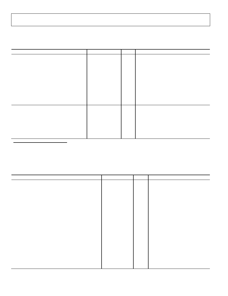
SPECIFICATIONS
V
S
= 3.3 V ± 5%; V
S
V
CP
5.5 V, T
A
= 25°C, R
SET
= 4.12 k, CPR
SET
= 5.1 k, unless otherwise noted.
PLL CHARACTERISTICS
Table 1.
Parameter Min
Typ
Max
Unit
Test
Conditions/Comments
REFERENCE INPUTS (REFIN)
Input Frequency
0
250
MHz
Input Sensitivity, Differential
200
mV
Input Voltage, Single-Ended
1.1
1.7
V
REFINB capacitively bypassed to RF ground
Input Common-Mode Voltage
1.6
V
Self-bias voltage of REFINB
Input Capacitance
2
pF
Input Resistance
5
k
PHASE/FREQUENCY DETECTOR (PFD)
Phase Frequency Detector Input Frequency
80
MHz
Antibacklash pulse width 0D <1:0> = 00
Phase Frequency Detector Input Frequency
MHz
Antibacklash pulse width 0D <1:0> = 01
Phase Frequency Detector Input Frequency
MHz
Antibacklash pulse width 0D <1:0> = 10
Antibacklash Pulse Width
1.3
ns
0D <1:0> = 00
Antibacklash Pulse Width
2.9
ns
0D <1:0> = 01
Antibacklash Pulse Width
6.0
ns
0D <1:0> = 10
CHARGE PUMP (CP)
I
CP
Sink/Source
Programmable
High Value
5
mA
Low Value
625
µA
Absolute Accuracy
2.5
%
V
CP
= V
S
/2
R
SET
Range
2.7/10
k
I
CP
Three-State Leakage
1
nA
Sink and Source Current Matching
2
%
0.5 V < CP < V
CP
- 0.5 V
I
CP
vs. V
CP
1.5
%
0.5 V < CP < V
CP
- 0.5 V
I
CP
vs. Temperature
2
%
CP = V
S
/2
RF CHARACTERISTICS
(CLK2 - PLL FEEDBACK)
CLK2 is electrically identical to CLK1, the
distribution only input (see Clock Inputs); can
be used as differential or single-ended inputs
Input Frequency
1.5
GHz
Frequencies > 800 MHz require a minimum
divide-by-2 see the Distribution section
Input Sensitivity, Differential
200
mV
Input Common-Mode Voltage, V
CM
1.6
V
Self biased; enables ac coupling
Input Single-Ended Sensitivity
V
CM
± 100
mV
When dc-coupled, B input capacitively
bypassed to RF ground
Input Resistance
5
k
Input Capacitance
2
pF
AD9510
Preliminary Technical Data
Rev. PrA | Page 4 of 41
Parameter Min
Typ
Max
Unit
Test
Conditions/Comments
NOISE
CHARACTERISTICS
In-band noise of the charge pump/
phase frequency detector (inband
means within the LBW of the PLL)
The synthesizer phase noise floor is estimated
by measuring the in-band phase noise at
the output of the VCO and subtracting 20logN
(where N is the N divider value).
@ 50 kHz PFD Frequency
-172
dBc/Hz
@ 2 MHz PFD Frequency
-156
dBc/Hz
@ 10 MHz PFD Frequency
-149
dBc/Hz
@ 50 MHz PFD Frequency
-142
dBc/Hz
PLL Figure of Merit
-219 + 10 × log
(f
PFD
)
dBc/Hz
Approximation of the PFD/CP phase noise
floor (in the flat region) inside the PLL loop
bandwidth. When running closed loop this
phase noise is gained up by 20 × log(N)
1
PRESCALER
Prescaler Input Frequency
P = 2 DM (2/3)
500
MHz
P = 4 DM (4/5)
750
MHz
P = 8 DM (8/9)
1500
MHz
P = 16 DM (16/17)
1500
MHz
P = 32 DM (32/33)
1500
MHz
Prescaler Output Frequency
300
MHz
PLL DIGITAL LOCK DETECT WINDOW
Signal available at STATUS pin
when selected by 08h <5:2>
Required to Lock (Coincidence of Edges)
Selected by register ODh
Low Range
3.5
ns
<5> = 1
High Range
9.5
ns
<5> = 0
To Unlock after Lock (Hysteresis)
Selected by register ODh
Low Range
7
ns
<5> = 1
High Range
15
ns
<5> = 0
1
Example: -219 + 10 × log (f
PFD
) + 20 × log(N) should give the values for the in-band noise at the VCO output.
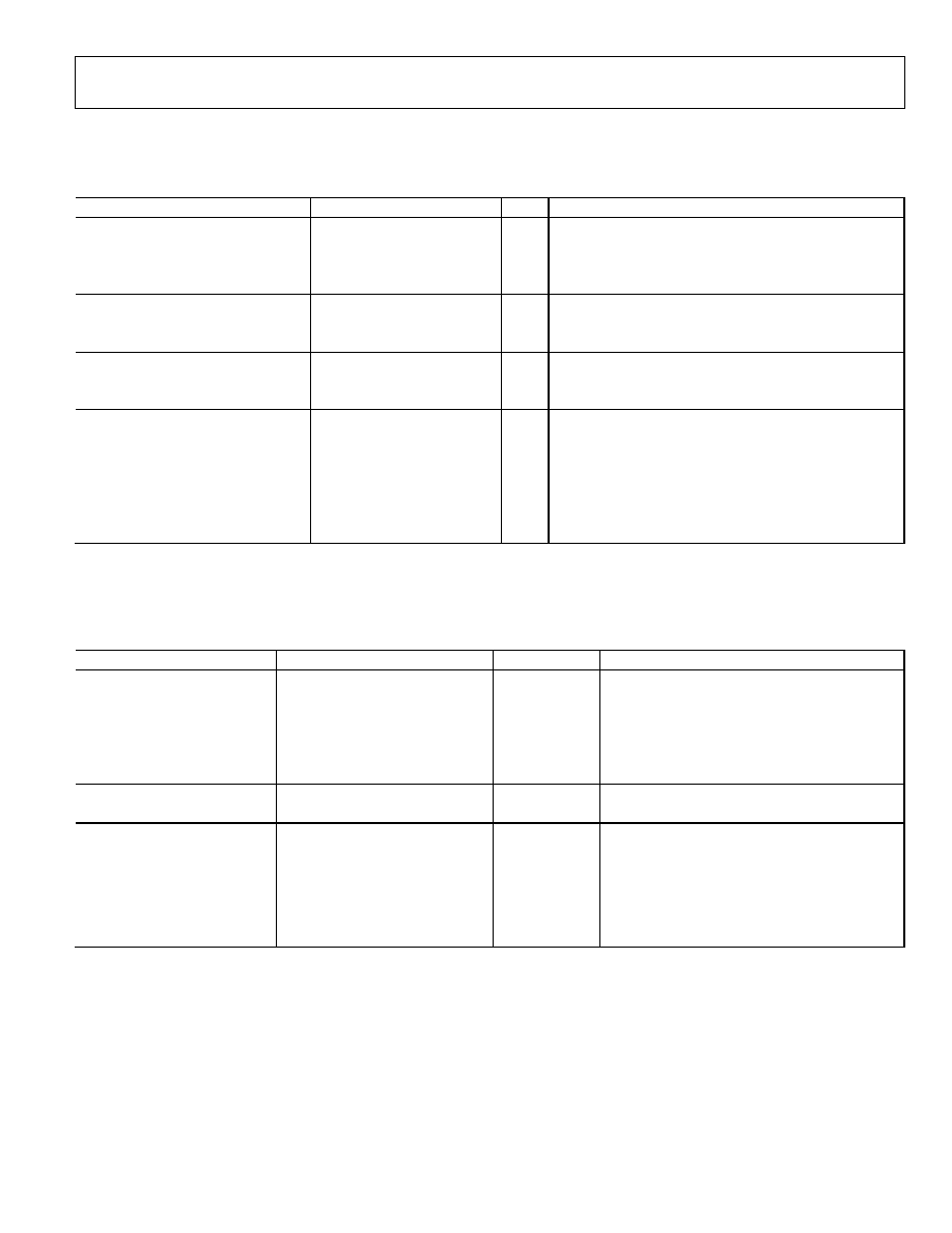
CLOCK INPUTS
Table 2.
Parameter
Min
Typ
Max
Unit
Test Conditions/Comments
CLOCK INPUTS
CLK1 and CLK2 are electrically
identical; can be used as differential
or single-ended inputs
Input Frequency
1.5
GHz
Frequencies > 800 MHz require a
minimum divide-by-2 see the
Distribution section
Input Sensitivity, Differential
200
mV
Input Common-Mode Voltage , V
CM
1.6
V
Self-biased; enables ac coupling
Input Single-Ended Sensitivity
V
CM
± 100
mV
When dc-coupled, B input capacitively
bypassed to RF ground
Input Resistance
5
k
Self-biased
Input Capacitance
2
pF
CLK1 to CLK2 Isolation
dB
Preliminary Technical Data
AD9510
Rev. PrA | Page 5 of 41
CLOCK OUTPUTS
Table 3.
Parameter
Min
Typ
Max
Unit
Test Conditions/Comments
LVPECL CLOCK OUTPUTS
Termination = 50 to V
S
- 2 V; default
OUT0, OUT1 OUT2, OUT3; Differential
Output level setting 3C (3D) (3E) (3F)
<3:2> = 10
Output Frequency
800
MHz
Output High Voltage (V
OH
) V
S
- 1.2
V
S
- 0.8
V
@ dc
Output Low Voltage (V
OL
) V
S
- 1.8
V
S
- 1.6
V
@ dc
Output Differential Voltage (V
OD
)
800
mV
@ dc
Isolation LVPECL to LVPECL Output
dB
100 MHz output with 50 MHz aggressor
Isolation LVDS to LVPECL Output
dB
100 MHz output with 50 MHz aggressor
Isolation CMOS to LVPECL Output
dB
100 MHz output with 50 MHz aggressor
LVDS CLOCK OUTPUTS
Termination = 100 differential; default
OUT4, OUT5, OUT6, OUT7; Differential
Output Level setting 40 (41) (42) (43)
<2:1> = 01, 3.5 mA termination current
Output Frequency
800
MHz
Differential Output Voltage (V
OD
)
350
mV
Delta V
OD
5
mV
Output Offset Voltage (V
OS
)
1.25
V
Delta V
OS
5
mV
Short-Circuit Current (I
SA
, I
SB
)
13
mA
Output shorted to GND
Isolation LVDS to LVDS
dB
100 MHz output with 50 MHz aggressor
Isolation LVPECL to LVDS
dB
100 MHz output with 50 MHz aggressor
Isolation CMOS to LVDS
dB
100 MHz output with 50 MHz aggressor
CMOS CLOCK OUTPUTS
B outputs are inverted;
termination = open
OUT4, OUT5, OUT6, OUT7; Single Ended
Output Frequency
250
MHz
5 pF load
Output Voltage High (V
OH
)
2.7
V
Output Voltage Low (V
OL
)
0.4
V
Isolation CMOS to CMOS
dB
100 MHz output with 50 MHz aggressor
Isolation LVPECL to CMOS
dB
100 MHz output with 50 MHz aggressor
Isolation LVDS to CMOS
dB
100 MHz output with 50 MHz aggressor
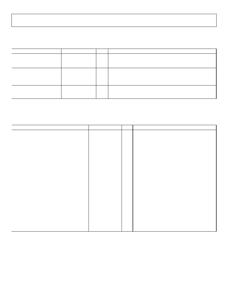
TIMING CHARACTERISTICS
Table 4.
Parameter
Min
Typ
Max
Unit
Test Conditions/Comments
LVPECL
Termination = 50 to V
S
- 2 V; default
Output level setting 3C (3D) (3E) (3F) <3:2> = 10
Output Rise Time, t
RP
120
ps
20% to 80%
Output Fall Time, t
FP
120
ps
80% to 20%
CLK-TO-LVPECL OUT
CLK1 or CLK2
Propagation Delay, t
PECL
Divide = Bypass
0.65
ns
Divide = 2 - 32
0.65
ns
Output Skew, t
SKP
25
50
ps
LVPECL to LVPECL on same part
1
Output Skew, t
SKP_AB
150
300
ps
LVPECL to LVPECL on different parts
2
AD9510
Preliminary Technical Data
Rev. PrA | Page 6 of 41
Parameter
Min
Typ
Max
Unit
Test Conditions/Comments
LVDS
Termination = 100 differential; default
Output level setting 40 (41) (42) (43)
<2:1> = 01, 3.5 mA termination current
Output Rise Time, t
RL
250
ps
20% to 80%
Output Fall Time, t
FL
250
ps
80% to 20%
CLK-TO-LVDS OUT
Propagation Delay, t
LVDS
Divide = Bypass
1.4
ns
Divide = 2 - 32
1.4
ns
Output Skew, t
SKL
50
100
ps
OUT4 to OUT7 on same part
Output Skew, t
SKL_AB
200
400
ps
LVDS on different parts
CLK-TO-LVDS OUT DELAY ADJUST CHANNEL
Delay off
Propagation Delay, t
LVDSD
OUT5 to OUT6 on same part
Divide = Bypass
1.45
ns
Divide = 2 - 32
1.45
ns
Output Skew, t
SKLD
50
100
ps
OUT5 to OUT6 on same part
CMOS
B outputs are inverted; termination = open
Output Rise Time, t
RL
300
ps
20% to 80%; C
LOAD
= 3 pF
Output Fall Time, t
FL
300
ps
80% to 20%; C
LOAD
= 3 pF
CLK-TO-CMOS OUT
Propagation Delay, t
CMOS
C
LOAD
= 3 pF
Divide = Bypass
1.4
ns
Divide = 2 - 32
1.4
ns
Output Skew, t
SKC
50
150
ps
CMOS to CMOS on same part
Output Skew, t
SKC_AB
200
400
ps
CMOS to CMOS on different parts
CLK-TO-CMOS OUT DELAY ADJUST CHANNEL
Delay off
Propagation Delay, t
CMOSD
C
LOAD
= 3 pF
Divide = Bypass
1.45
ns
Divide = 2 - 32
1.45
ns
Output Skew, t
SKCD
50
150
ps
OUT5 to OUT6 on same part
LVPECL-TO-LVDS OUT
Everything the same; different logic
Output Skew, t
SKP_L
0.75
ns
LVPECL to LVDS on same part
LVPECL-TO-CMOS OUT
Everything the same; different logic
Output Skew, t
SKP_C
0.75
ns
LVPECL to CMOS on same part
LVDS-TO-CMOS OUT
Everything the same; different logic
Output Skew, t
SKL_C
100
150
ps
LVDS to CMOS on same part
DELAY ADJUST
OUT5 (OUT6); LVDS and CMOS
Shortest Delay Range
35h (39h) <5:0> 111111
Zero Scale
0.3
ns
36h (3Ah) <5:0> 000000
Full Scale
1.0
ns
36h (3Ah) <5:0> 111111
Linearity
%LSB
Longest Delay Range
35h (39h) <5:0> 000000
Zero Scale
0.5
ns
36h (3Ah) <5:0> 000000
Full Scale
10
ns
36h (3Ah) <5:0> 111111
Linearity
%LSB
1
Defined as the worst-case difference between any two similar delay paths within a single device operating at the same voltage and temperature.
2
Defined as the absolute worst-case difference between any two delay paths on any two devices operating at the same voltage and temperature. Part-to-part skew is
the total skew difference; pin-to-pin skew + part-to-part skew.
Preliminary Technical Data
AD9510
Rev. PrA | Page 7 of 41
CLOCK OUTPUT PHASE NOISE
Table 5.
Parameter Min
Typ
Max
Unit
Test
Conditions/Comments
CLK1 TO LVPECL ADDITIVE PHASE NOISE
Distribution section only; does not
include PLL or external VCO/VCXO
CLK1 = 622.08 MHz, OUTN = 622.08 MHz
Input slew rate > 1 V/ns
Divide Ratio = 1
@ 10 Hz Offset
-125
dBc/Hz
@ 100 Hz Offset
-132
dBc/Hz
@ 1 kHz Offset
-140
dBc/Hz
@ 10 kHz Offset
-148
dBc/Hz
@ 100 kHz Offset
-153
dBc/Hz
>1 MHz Offset
-154
dBc/Hz
CLK1 = 622.08 MHz, OUTN = 155.52 MHz
Divide Ratio = 4
@ 10 Hz Offset
-130
dBc/Hz
@ 100 Hz Offset
-140
dBc/Hz
@ 1 kHz Offset
-148
dBc/Hz
@ 10 kHz Offset
-155
dBc/Hz
@ 100 kHz Offset
-161
dBc/Hz
>1 MHz Offset
-161
dBc/Hz
CLK1 = 622.08 MHz, OUTN = 38.88 MHz
Divide Ratio = 16
@ 10 Hz Offset
-145
dBc/Hz
@ 100 Hz Offset
-152
dBc/Hz
@ 1 kHz Offset
-161
dBc/Hz
@ 10 kHz Offset
-165
dBc/Hz
@ 100 kHz Offset
-165
dBc/Hz
>1 MHz Offset
-166
dBc/Hz
CLK1 = 491.52 MHz, OUTN = 61.44 MHz
Divide Ratio = 8
@ 10 Hz Offset
-131
dBc/Hz
@ 100 Hz Offset
-142
dBc/Hz
@ 1 kHz Offset
-153
dBc/Hz
@ 10 kHz Offset
-160
dBc/Hz
@ 100 kHz Offset
-165
dBc/Hz
> 1 MHz Offset
-165
dBc/Hz
CLK1 = 491.52 MHz, OUTN = 245.76 MHz
Divide Ratio = 2
@ 10 Hz Offset
-127
dBc/Hz
@ 100 Hz Offset
-136
dBc/Hz
@ 1 kHz Offset
-144
dBc/Hz
@ 10 kHz Offset
-153
dBc/Hz
@ 100 kHz Offset
-157
dBc/Hz
>1 MHz Offset
-158
dBc/Hz
CLK1 = 245.76 MHz, OUTN = 61.44 MHz
Divide Ratio = 4
@ 10 Hz Offset
-140
dBc/Hz
@ 100 Hz Offset
-144
dBc/Hz
@ 1 kHz Offset
-154
dBc/Hz
@ 10 kHz Offset
-163
dBc/Hz
@ 100 kHz Offset
-164
dBc/Hz
AD9510
Preliminary Technical Data
Rev. PrA | Page 8 of 41
Parameter Min
Typ
Max
Unit
Test
Conditions/Comments
>1 MHz Offset
-165
dBc/Hz
CLK1-TO-LVDS ADDITIVE PHASE NOISE
Distribution section only; does not
include PLL or external VCO/VCXO
Characterization ongoing
CLK1 = 622.08 MHz, OUTN = 622.08 MHz
Divide Ratio = 1
@ 10 Hz Offset
dBc/Hz
@ 100 Hz Offset
dBc/Hz
@ 1 kHz Offset
dBc/Hz
@ 10 kHz Offset
dBc/Hz
@ 100 kHz Offset
dBc/Hz
>1 MHz Offset
dBc/Hz
CLK1 = 622.08 MHz, OUTN = 155.52 MHz
Divide Ratio = 4
@ 10 Hz Offset
dBc/Hz
@ 100 Hz Offset
dBc/Hz
@ 1 kHz Offset
dBc/Hz
@ 10 kHz Offset
dBc/Hz
@ 100 kHz Offset
dBc/Hz
>1 MHz Offset
dBc/Hz
CLK1 = 622.08 MHz, OUTN = 38.88 MHz
Divide Ratio = 16
@ 10 Hz Offset
dBc/Hz
@ 100 Hz Offset
dBc/Hz
@ 1 kHz Offset
dBc/Hz
@ 10 kHz Offset
dBc/Hz
@ 100 kHz Offset
dBc/Hz
>1 MHz Offset
dBc/Hz
CLK1 = 491.52 MHz, OUTN = 61.44 MHz
Divide Ratio = 8
@ 10 Hz Offset
dBc/Hz
@ 100 Hz Offset
dBc/Hz
@ 1 kHz Offset
dBc/Hz
@ 10 kHz Offset
dBc/Hz
@ 100 kHz Offset
dBc/Hz
> 1 MHz Offset
dBc/Hz
CLK1 = 491.52 MHz, OUTN = 245.76 MHz
Divide Ratio = 2
@ 10 Hz Offset
dBc/Hz
@ 100 Hz Offset
dBc/Hz
@ 1 kHz Offset
dBc/Hz
@ 10 kHz Offset
dBc/Hz
@ 100 kHz Offset
dBc/Hz
>1 MHz Offset
dBc/Hz
CLK1 = 245.76 MHz, OUTN = 61.44 MHz
Divide Ratio = 4
@ 10 Hz Offset
dBc/Hz
@ 100 Hz Offset
dBc/Hz
@ 1 kHz Offset
dBc/Hz
@ 10 kHz Offset
dBc/Hz
@ 100 kHz Offset
dBc/Hz
>1 MHz Offset
dBc/Hz
Preliminary Technical Data
AD9510
Rev. PrA | Page 9 of 41
Parameter Min
Typ
Max
Unit
Test
Conditions/Comments
CLK1 to CMOS ADDITIVE PHASE NOISE
Distribution section only; does not
include PLL or external VCO/VCXO
CLK1 = 245.76 MHz, OUTN = 245.76 MHz
Divide Ratio = 1
@ 10 Hz Offset
-117
dBc/Hz
@ 100 Hz Offset
-124
dBc/Hz
@ 1 kHz Offset
-131
dBc/Hz
@ 10 kHz Offset
-141
dBc/Hz
@ 100 kHz Offset
-146
dBc/Hz
@ 1 MHz Offset
-150
dBc/Hz
> 10 MHz Offset
-156
dBc/Hz
CLK1 = 245.76 MHz, OUTN = 61.44 MHz
Divide Ratio = 4
@ 10 Hz Offset
-128
dBc/Hz
@ 100 Hz Offset
-136
dBc/Hz
@ 1 kHz Offset
-144
dBc/Hz
@ 10 kHz Offset
-152
dBc/Hz
@ 100 kHz Offset
-158
dBc/Hz
@ 1 MHz Offset
-160
dBc/Hz
>10 MHz Offset
-162
dBc/Hz
CLK1 = 78.6432 MHz, OUTN = 78.6432 MHz
Divide Ratio = 1
@ 10 Hz Offset
-127
dBc/Hz
@ 100 Hz Offset
-135
dBc/Hz
@ 1 kHz Offset
-142
dBc/Hz
@ 10 kHz Offset
-151
dBc/Hz
@ 100 kHz Offset
-156
dBc/Hz
@ 1 MHz Offset
-158
dBc/Hz
>10 MHz Offset
-160
dBc/Hz
CLK1 = 78.6432 MHz, OUTN = 39.3216 MHz
Divide Ratio = 2
@ 10 Hz Offset
-134
dBc/Hz
@ 100 Hz Offset
-140
dBc/Hz
@ 1 kHz Offset
-148
dBc/Hz
@ 10 kHz Offset
-156
dBc/Hz
@ 100 kHz Offset
-161
dBc/Hz
> 1 MHz Offset
-162
dBc/Hz
AD9510
Preliminary Technical Data
Rev. PrA | Page 10 of 41
CLOCK OUTPUT ADDITIVE TIME JITTER
1
Table 6.
Parameter Min
Typ
Max
Unit
Test
Conditions/Comments
LVPECL OUTPUT ADDITIVE TIME JITTER
Distribution section only;
does not include PLL or external VCO/VCXO
CLK1 = 622.08 MHz, OUT0:3 = 622.08 MHz
40
fs rms
BW = 12 kHz - 20 MHz
Divide Ratio = 1
(OC-12)
CLK1 = 622.08 MHz, OUT0:3 = 155.52 MHz
55
fs rms
BW = 12 kHz - 20 MHz
Divide Ratio = 4
(OC-3)
CLK1 = 200 MHz, OUT0:3 = 100 MHz
225
fs
rms
Calculated from SNR of ADC method;
F
C
= 100 MHz with A
IN
= 170 MHz
Divide Ratio = 2
LVDS OUTPUT ADDITIVE TIME JITTER
Distribution section only;
does not include PLL or external VCO/VCXO
CLK1 = 200 MHz, OUT4 = 100 MHz
275
fs
rms
Calculated from SNR of ADC method;
F
C
= 100 MHz with A
IN
= 170 MHz
CMOS OUTPUT ADDITIVE TIME JITTER
Distribution section only;
does not include PLL or external VCO/VCXO
CLK1 = 200 MHz, OUT4 = 100 MHz
275
fs
rms
Calculated from SNR of ADC method;
F
C
= 100 MHz with A
IN
= 170 MHz
1
Distribution section only; does not include PLL or external VCO/VCXO.
PLL AND DISTRIBUTION PHASE NOISE AND SPURIOUS
Table 7. PLL and Distribution
Parameter Min
Typ
Max
Unit
Test
Conditions/Comments
PHASE NOISE AND SPURIOUS
Depends on VCO/VCXO selection.
Characterization ongoing.
Setup No.1
Measured at LVPECL clock outputs;
ABP = 6 ns; I
CP
= 5 mA; Ref = 30.72 MHz
245.76 MHz VCXO, F
PFD
= 1.2288 MHz; R = 25, N = 200
245.76 MHz Output
Divide by 1
Phase Noise @100 kHz Offset
dBc/Hz
Spurious
dBc
First and second harmonics of F
PFD
61.44 MHz Output
Divide by 4
Phase Noise @100 kHz Offset
dBc/Hz
Spurious
dBc
First and second harmonics of F
PFD
Setup No. 2
Measured at LVPECL clock outputs;
ABP = 6 ns; I
CP
= 5 mA; Ref = 30.72 MHz
245.76 MHz VCXO, F
PFD
= 30.72 MHz; R = 1, N = 8
245.76 MHz Output
Divide by 1
Phase Noise @100 kHz Offset
dBc/Hz
Spurious
dBc
First and second harmonics of F
PFD
61.44 MHz Output
Divide by 4
Phase Noise @100 kHz Offset
dBc/Hz
Spurious
dBc
First and second harmonics of F
PFD
Preliminary Technical Data
AD9510
Rev. PrA | Page 11 of 41
SERIAL CONTROL PORT
Table 8.
Parameter
Min
Typ
Max
Unit
Test Conditions/Comments
SDIO, CSB, SCLK
CMOS Levels
Input Logic 1 Voltage
V
Input Logic 0 Voltage
V
Input Capacitance
pF
SDIO, SDO
CMOS Levels
Output Logic 1 Voltage
V
Output Logic 0 Voltage
V
CSB, SCLK
CMOS Levels
CSB and SCLK have 30 k internal pull-down resistors
Input Logic 1 Current
µA
Input Logic 0 Current
µA
TIMING
Clock Rate (SCLK, 1/t
SCLK
)
25
MHz
Pulse-Width High, t
PWH
16
24
ns
Pulse-Width Low, t
PWL
16
24
ns
SDIO and CSB to SCLK Setup, t
DS
ns
SCLK to SDIO Hold, t
DH
ns
SCLK to Valid SDIO and SDO, t
DV
ns
FUNCTION PIN
Table 9.
Parameter
Min
Typ
Max
Unit
Test Conditions/Comments
INPUT CHARACTERISTICS
CMOS Levels
Logic 1 Voltage
V
Logic 0 Voltage
V
Input Capacitance
pF
Logic 1 Current
µA
Logic 0 Current
µA
RESET TIMING
Pulse-Width Low
ns
SYNC TIMING
Pulse-Width Low
1.5
Clock cycles
Sync single chip; CLK1 or CL2,
whichever is being used for distribution
Setup Time
ps
Sync multichip; Write CLK1 or CLK2,
whichever is being used for distribution
Hold Time
ps
Sync multichip; Write CLK1 or CLK2,
whichever is being used for distribution
AD9510
Preliminary Technical Data
Rev. PrA | Page 12 of 41
STATUS PIN
Table 10.
Parameter
Min
Typ
Max
Unit
Test Conditions/Comments
OUTPUT CHARACTERISTICS
Output Voltage High (V
OH
)
mV
Output Voltage Low (V
OL
) mV
MAXIMUM TOGGLE RATE
100
MHz
Applies when PLL mux is set to any divider or counter output,
or PFD up/down pulse. Also applies in analog lock detect mode.
Usually debug mode only. Beware that spurs may couple
to output when this pin is toggling.
ANALOG LOCK DETECT
Capacitance
3
pF
On-chip capacitance; used to calculate RC time
constant for analog lock detect readback. Use pull-up resistor.
POWER
Table 11.
Parameter
Min
Typ
Max
Unit
Test Conditions/Comments
POWER-UP DEFAULT MODE POWER DISSIPATION
650
mW
Power-up default state; does not
include power dissipated in output
load resistors.
MAXIMUM POWER DISSIPATION
1050
mW
All functions enabled, all outputs on
and terminated, maximum clock rates,
and frequencies. Does not include
power dissipated in load resistors.
(Pick these conditions.)
POWER DELTA
CLK1, CLK2 Power-Down
mW
Divider, DIV 2 - 32 to Bypass
mW
LVPECL Output Power-Down
Safe Power-Down (PD2)
56
mW
PD2 mode (safe) power-down is required
when load resistors are connected. Delta
does not include dissipation in load resistors.
Total Power-Down (PD3)
58
mW
PD3 mode; use only with no load resistors connected.
LVDS Output Power-Down
33
46
mW
CMOS Output Power-Down
24
38
mW
Delay Block Bypass
mW
Delay Block Power-Down
mW
PLL Section Power-Down
40
mW
Preliminary Technical Data
AD9510
Rev. PrA | Page 13 of 41
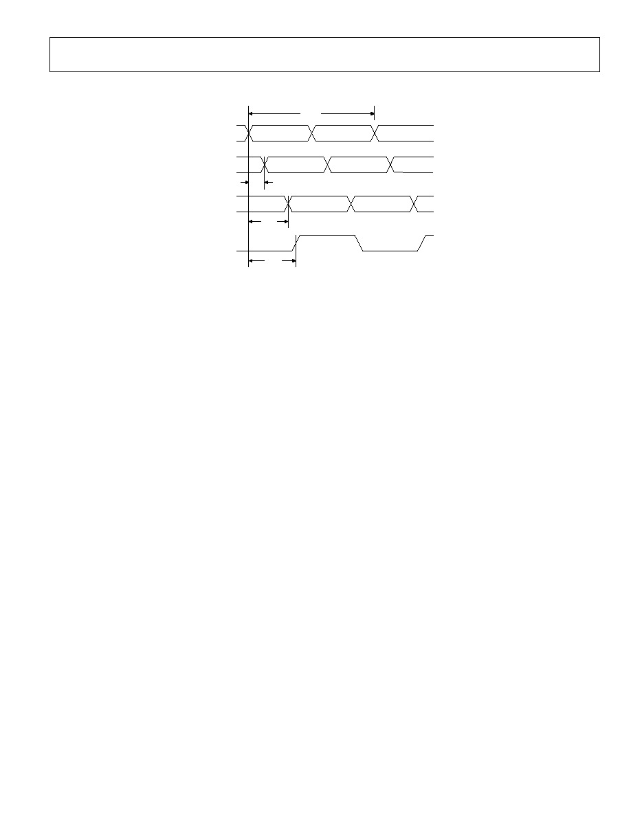
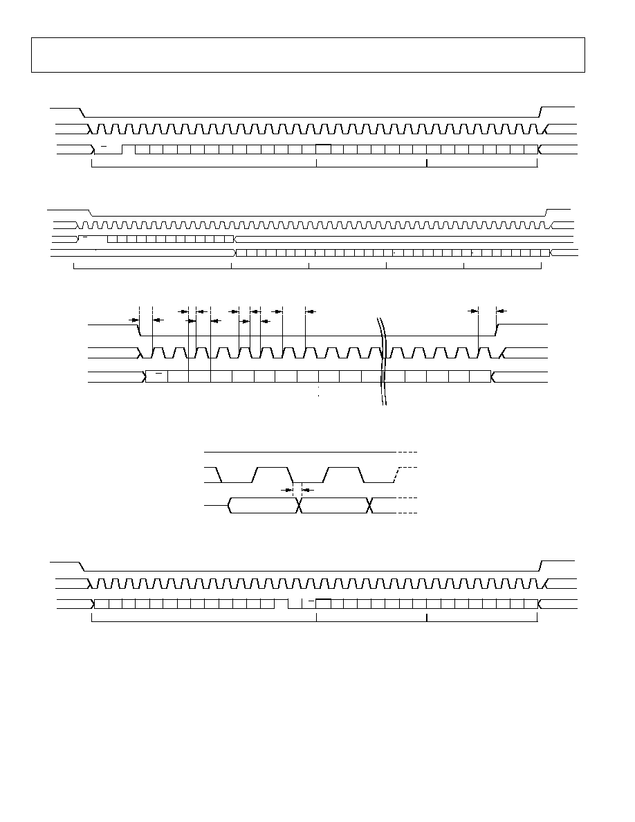
TIMING DIAGRAMS
t
CLK1
CLK1
t
LVDS
t
CMOS
t
PECL
Figure 2. CLK1/CLK1B to Clock Output Timing, DIV = 1 Mode
AD9510
Preliminary Technical Data
Rev. PrA | Page 14 of 41
ABSOLUTE MAXIMUM RATINGS
Table 12.
Parameter or Pin
With
Respect
to
Min Max Unit
V
S
GND
-0.3
+3.6
V
V
CP
GND
-0.3
+6
V
V
CP
V
S
-0.3
V
REFIN, REFINB
V
RSET GND
V
CPRSET GND
V
CLK1. CLK1B, CLK2, CLK2B
V
CLK1
CLK1B
V
CLK2
CLK2B
V
SCLK, SDIO SDO, CSB
GND
V
Outputs 0, 1, 2, 3
V
Outputs 4, 5, 6, 7
V
FUNCTION
V
STATUS
V
Junction Temperature
150
°C
Storage Temperature
-65
+150
°C
Lead Temperature (10 sec)
300
°C
Stresses above those listed under Absolute Maximum Ratings
may cause permanent damage to the device. This is a stress
rating only; functional operation of the device at these or any
other conditions above those indicated in the operational
sections of this specification is not implied. Exposure to
absolute maximum ratings for extended periods may affect
device reliability.
THERMAL CHARACTERISTICS
1
Thermal Resistance
64-Lead LFCSP
JA
= 24°C/W
1
Thermal impedance measurements were taken on a 4-layer board in still air,
in accordance with EIA/JESD51-7.
ESD CAUTION
ESD (electrostatic discharge) sensitive device. Electrostatic charges as high as 4000 V readily accumulate on
the human body and test equipment and can discharge without detection. Although this product features
proprietary ESD protection circuitry, permanent damage may occur on devices subjected to high energy
electrostatic discharges. Therefore, proper ESD precautions are recommended to avoid performance
degradation or loss of functionality.
Preliminary Technical Data
AD9510
Rev. PrA | Page 15 of 41
PIN CONFIGURATION AND FUNCTION DESCRIPTIONS
PIN 1
INDICATOR
17
18
19
20
21
22
23
24
25
26
27
28
29
30
31
32
S
T
ATUS
SC
LK
SD
IO
SD
O
CS
B
GND
VS
OUT7B
OUT7
VS
GND
OUT3B
OUT3
VS
VS
GND
64
63
62
61
60
59
58
57
56
55
54
53
52
51
50
49
VS
CP
RS
E
T
GND
R
SET
VS
VS
OUT0
OUT0B
VS
GND
OUT1
OUT1B
VS
VS
GND
GND
1
2
3
4
5
6
7
8
9
10
11
12
13
14
15
16
REFIN
REFINB
GND
VS
VCP
CP
GND
GND
VS
CLK2
CLK2B
GND
VS
CLK1
CLK1B
FUNCTION
VS
OUT4
OUT4B
VS
VS
OUT5
OUT5B
VS
VS
OUT6
OUT6B
VS
VS
OUT2
OUT2B
VS
48
47
46
45
44
43
42
41
40
39
38
37
36
35
34
33
AD9510
TOP VIEW
(Not to Scale)
05046-002
Figure 3. 64-Lead LFCSP Pin Configuration
Note that the exposed paddle on this package is an electrical connection as well as a thermal enhancement. For the device to
function properly, the paddle must be attached to ground, GND.
AD9510
Preliminary Technical Data
Rev. PrA | Page 16 of 41
Table 13. Pin Function Descriptions
Pin No.
Mnemonic Description
1
REFIN
PLL Reference Input.
2
REFINB
Complementary PLL Reference Input.
3, 7, 8, 12, 22,
27, 32, 49, 50,
55, 62
GND Ground.
4, 9, 13, 23, 26,
30, 31, 33, 36,
37, 40, 41, 44,
45, 48, 51, 52,
56, 59, 60, 64
VS
Power Supply (3.3 V).
5 VCP
Charge Pump Power Supply. It should be greater than or equal to VS. VCP may be set as high as 5.5 V for
VCOs requiring extended tuning range.
6
CP
Charge Pump Output.
10 CLK2
Clock Input Used to Connect External VCO/VCXO to Feedback Divider, N. CLK2 also drives the distribution
section of the chip and may be used as a generic clock input when PLL is not used.
11
CLK2B
Complementary Clock Input Used in Conjunction with CLK2.
14
CLK1
Clock Input That Drives Distribution Section of the Chip.
15
CLK1B
Complementary Clock Input Used in Conjunction with CLK1.
16
FUNCTION
Multipurpose Input May Be Programmed as a Reset (RESETB), Sync (SYNCB), or Power-Down (PDB) Pin.
17
STATUS
Output Used to Monitor PLL Status and Sync Status.
18
SCLK
Serial Data Clock.
19
SDIO
Serial Data I/O.
20
SDO
Serial Data Output.
21
CSB
Serial Port Chip Select.
24
OUT7B
Complementary LVDS/Inverted CMOS Output.
25
OUT7
LVDS/CMOS Output.
28
OUT3B
Complementary LVPECL Output.
29
OUT3
LVPECL Output.
34
OUT2B
Complementary LVPECL Output.
35
OUT2
LVPECL Output.
38
OUT6B
Complementary LVDS/Inverted CMOS Output. OUT6 includes a delay block.
39
OUT6
LVDS/CMOS Output. OUT6 includes a delay block.
42 OUT5B
Complementary
LVDS/Inverted
CMOS Output. OUT5 includes a delay block.
43
OUT5
LVDS/CMOS Output. OUT5 includes a delay block.
46
OUT4B
Complementary LVDS/Inverted CMOS Output.
47 OUT4
LVDS/CMOS
Output.
53
OUT1B
Complementary LVPECL Output.
54 OUT1
LVPECL
Output.
57
OUT0B
Complementary LVPECL Output.
58 OUT0
LVPECL
Output.
61
RSET
Current Set Resistor to Ground. Nominal value = 4.147 k.
63
CPRSET
Charge Pump Current Set Resistor to Ground. Nominal value = 5.1 k.
Note that the exposed paddle on this package is an electrical connection as well as a thermal enhancement. For the device to
function properly, the paddle must be attached to ground, GND.

Preliminary Technical Data
AD9510
Rev. PrA | Page 17 of 41
TERMINOLOGY
Phase Jitter and Phase Noise
An ideal sine wave can be thought of as having a continuous
and even progression of phase with time from 0 to 360 degrees
for each cycle. Actual signals, however, display a certain amount
of variation from ideal phase progression over time. This
phenomenon is called phase jitter. Although there are many
causes that can contribute to phase jitter, one major component
is due to random noise which is characterized statistically as
being Gaussian (normal) in distribution.
This phase jitter leads to a spreading out of the energy of the
sine wave in the frequency domain, producing a continuous
power spectrum. This power spectrum is usually reported as a
series of values whose units are dBc/Hz at a given offset in
frequency from the sine wave (carrier). The value is a ratio
(expressed in dB) of the power contained within a 1 Hz
bandwidth with respect to the power at the carrier frequency.
For each measurement the offset from the carrier frequency is
also given.
It is also meaningful to integrate the total power contained
within some interval of offset frequencies (for example, 10 kHz
to 10 MHz). This is called the integrated phase noise over that
frequency offset interval and can be readily related to the time
jitter due to the phase noise within that offset frequency
interval.
Phase noise has a detrimental effect on the performance of
ADCs and DACs and RF mixers. It lowers the achievable
dynamic range of the converters and mixers, although they are
affected in somewhat different ways.
Time Jitter
Phase noise is a frequency domain phenomenon. In the time
domain, the same effect is exhibited as time jitter. When
observing a sine wave, the time of successive zero crossings is
seen to vary. In the case of a square wave, the time jitter is seen
as a displacement of the edges from their ideal (regular) times
of occurrence. In both cases, the variations in timing from the
ideal are the time jitter. Since these variations are random in
nature, the time jitter is specified in units of seconds root mean
square (rms) or 1 sigma of the Gaussian distribution.
Time jitter that occurs on a sampling clock for a DAC or an
ADC decreases the SNR and dynamic range of the converter. A
sampling clock with the lowest possible jitter provides the
highest performance from a given converter.
Additive Phase Noise
It is the amount of phase noise that is attributable to the device
or subsystem being measured. The phase noise of any external
oscillators or clock sources has been subtracted. This makes it
possible to predict the degree to which the device impacts the
total system phase noise when used in conjunction with the
various oscillators and clock sources, each of which contribute
their own phase noise to the total. In many cases, the phase
noise of one element dominates the system phase noise.
Additive Time Jitter
It is the amount of time jitter that is attributable just to the
device or subsystem being measured. The time jitter of any
external oscillators or clock sources has been subtracted. This
makes it possible to predict the degree to which the device will
impact the total system time jitter when used in conjunction
with the various oscillators and clock sources, each of which
contribute their own time jitter to the total. In many cases, the
time jitter of the external oscillators and clock sources
dominates the system time jitter.
AD9510
Preliminary Technical Data
Rev. PrA | Page 18 of 41
TYPICAL PERFORMANCE CHARACTERISTICS
Figure 4. Phase Noise - LVPECL 245.76 MHz
Figure 5. Phase Noise - LVPECL 622MHz
Figure 6. Phase Noise - CMOS 61.44MHz
Figure 7. Phase Noise - CMOS 245.76 MHz
Figure 8.
Figure 9.
Preliminary Technical Data
AD9510
Rev. PrA | Page 19 of 41
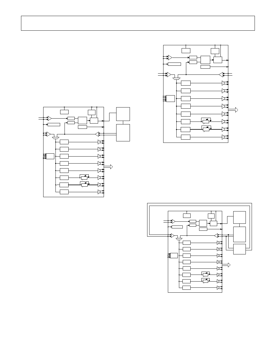
TYPICAL MODES OF OPERATION
PLL with External VCXO/VCO Followed by Clock
Distribution
This is the most common operational mode for the AD9510. An
external oscillator (shown as VCO/VCXO) is phase locked to a
reference input frequency applied to REFIN. The loop filter is
usually a passive design. A VCO or a VCXO may be used. The
CLK2 input is connected internally to the feedback divider, N.
The CLK2 input provides the feedback path for the PLL. If the
VCO/VCXO frequency exceeds maximum frequency of the
output(s) being used, an appropriate divide ratio must be set in
the corresponding divider(s) in the distribution section.
CP
Divide
CLK2
Serial
Port
PFD
R
Divide
REFIN
CLK1
Divide
N
Function
Divide
Divide
LVDS/
CMOS
LVDS/
CMOS
LVDS/
CMOS
Divide
Divide
Divide
LVPECL
LVPECL
LVPECL
LVPECL
LVDS/
CMOS
Status
Vref
Loop
Filter
VCXO,
VCO
AD9510
Reference
Input
Clock
Outputs
PLL
Ref
T
T
Figure 10. PLL and Clock Distribution Mode
Clock Distribution Only
In this mode, the PLL is not used. A customer can save power by
initiating a PLL power-down and by powering down any
unused clock channels.
In distribution mode, both CLK1 and CLK2 inputs are available
for distribution to outputs via a low jitter multiplexer (MUX).
CP
Divide
CLK2
Serial
Port
PFD
R
Divide
REFIN
CLK1
Divide
N
Function
Divide
Divide
LVDS/
CMOS
LVDS/
CMOS
LVDS/
CMOS
Divide
Divide
Divide
LVPE CL
LVPE CL
LVPE CL
LVPE CL
LVDS/
CMOS
Status
Vref
PLL
Ref
AD9510
Clock
Outputs
Clock
Input 1
Clock
Input 2
T
T
Figure 11. Clock Distribution Mode
PLL with External VCO and Band-Pass Filter Followed by
Clock Distribution
An external band-pass filter may be used to possibly improve
the phase noise and spurious characteristics of the PLL output.
This option is most appropriate when the desire is to optimize
cost by choosing a less expensive VCO combined with a
moderately priced filter. Note that the BPF is shown outside of
the VCO to N divider path, with the BP filter outputs routed to
CLK1.
CP
Divide
CLK2
Serial
Port
PFD
R
Divide
REFIN
CLK1
Divide
N
Function
Divide
Divide
LVDS/
CMOS
LVDS/
CMOS
LVDS/
CMOS
Divide
Divide
Divide
LVPECL
LVPECL
LVPECL
LVPECL
LVDS/
CMOS
Status
Vref
Loop
Filter
VCO
AD9510
Reference
Input
Clock
Outputs
BPF
PLL
Ref
T
T
Figure 12. AD9510 with VCO and BPF Filter
AD9510
Preliminary Technical Data
Rev. PrA | Page 20 of 41
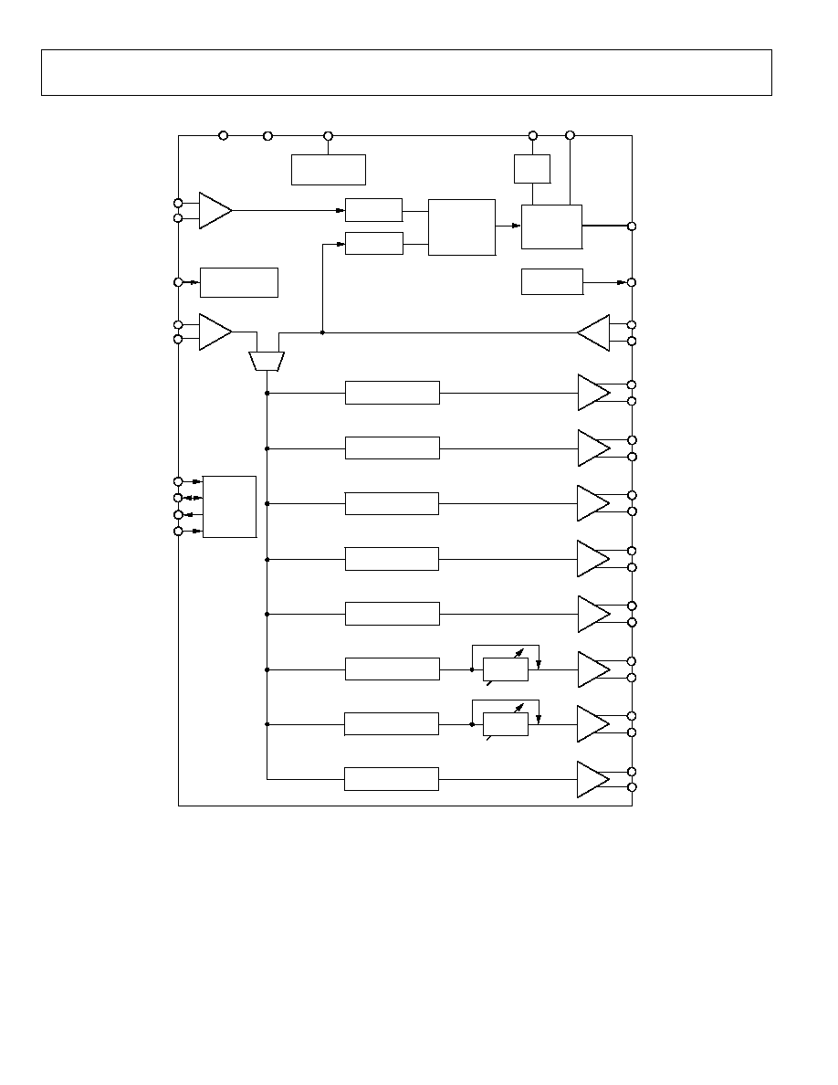
VS
GND
RSET
CPRSET
VCP
CP
STATUS
CLK2
CLK2B
OUT0
OUT0B
OUT1
OUT1B
OUT2
OUT2B
OUT3
OUT3B
OUT4
OUT4B
OUT5
OUT5B
OUT6
OUT6B
OUT7
OUT7B
SCLK
SDIO
SDO
CSB
/1, /2, /3 ... /31, /32
/1, /2, /3 ... /31, /32
/1, /2, /3 ... /31, /32
/1, /2, /3 ... /31, /32
/1, /2, /3 ... /31, /32
/1, /2, /3 ... /31, /32
/1, /2, /3 ... /31, /32
/1, /2, /3 ... /31, /32
PROGRAMMABLE DIVIDERS
LVDS/CMOS
LVDS/CMOS
LVDS/CMOS
LVDS/CMOS
LVPECL
LVPECL
LVPECL
LVPECL
CHARGE
PUMP
PLL
REF
PHASE
FREQUENCY
DETECTOR
R DIVIDER
N DIVIDER
DISTRIBUTION
REF
SYNCB,
RESETB PDB
CLK1B
CLK1
FUNCTION
REFINB
REFIN
SERIAL
CONTROL
PORT
PLL
SETTINGS
05 046- 001
AD9510
T
T
& PHASE ADJUST
Figure 13. Functional Block Diagram

Preliminary Technical Data
AD9510
Rev. PrA | Page 21 of 41
FUNCTION DESCRIPTION
OVERALL
Figure 13 shows a block diagram of the AD9510. The chip
combines a programmable PLL core with a configurable clock
distribution system. A complete PLL requires the addition of a
suitable external VCO (or VCXO) and loop filter. This PLL can
be used to lock to a reference input signal and produce an
output that is related to the input frequency by the ratio defined
by the programmable R and N dividers. The PLL offers some
jitter clean up of the external reference signal, depending on the
loop bandwidth and the phase noise performance of the VCO
(VCXO).
The output from the VCO (VCXO) can be applied to the clock
distribution section of the chip, where it can be divided by any
integer value from 1 to 32. The duty cycle and relative phase of
the outputs can be selected. There are four LVPECL outputs,
(OUT0, OUT1, OUT2, and OUT3) and four outputs that can be
selected as either LVDS or CMOS level outputs (OUT4, OUT5,
OUT6, and OUT7). Two of these outputs (OUT5, OUT6) can
also make use of a variable delay block.
Alternatively, the clock distribution section can be driven
directly by an external clock signal, and the PLL can be powered
off. Whenever the clock distribution section is used alone, there
is no clock clean-up. The jitter of the input clock signal is passed
along directly to the distribution section and may dominate at
the clock outputs.
PLL OPERATION
The AD9510 has a complete PLL core on-chip, requiring only
an external loop filter and VCO/VCXO. This PLL is based on
the ADF4106, a PLL noted for its superb low phase noise
performance. The operation of the AD9510 PLL is nearly
identical to that of the ADF4106, offering an advantage to those
with experience with the ADF series of PLLs. Differences
include the addition of differential inputs at REFIN and CLK2, a
different control register architecture, and the prescaler has
been changed to allow N as low as 1. The AD9510 PLL also
implements the digital lock detect feature somewhat differently
than does the ADF4106 offering improved functionality at
higher PFD rates. Refer to Register Map Description for details.
The PLL section can be used entirely separately from the
distribution system, if so desired.
PLL REFERENCE INPUT
The REFIN and REFINB pins can be driven differentially or
single-ended. These pins are internally self-biased, so they
should always be capacitively coupled. This also applies to the
unused side when single-ended input is used.
PLL REFERENCE DIVIDER
The REFIN/REFINB inputs are routed to reference divider, R,
which is a 14-bit counter. R may be programmed to any value
from 0 to 16383 via its control register. The output of the R
divider goes to one of the phase/frequency detector inputs. The
maximum allowable frequency into the phase/frequency
detector (PFD) must not be exceeded. This means that the
REFIN frequency divided by R must be less than the maximum
allowable PFD frequency.
VCO/VCXO CLOCK INPUT
The CLK2 differential input may be used as a second
distribution input, or it may be used to connect an external
VCO or VCXO to the PLL . Only the CLK2 input port has a
connection to the PLL N divider. This input can receive up to
1.5 GHz. These inputs are internally self-biased and must be
capacitively coupled.
CLK1 is electrically identical, but normally feeds the
distribution section instead. See Figure 16 for the equivalent
circuit of CLK1/CLK2.
VCO/VCXO FEEDBACK DIVIDER
The N divider is a combination of a prescaler and two counters,
A and B. Although the AD9510's PLL is similar to the ADF4106,
the AD9510 has a redesigned prescaler that allows for lower
values of N. The prescaler has both a dual modulus (DM) mode
and a fixed divide (FD) mode. The AD9510 prescaler modes are
shown in Table 14.
Table 14. PLL Prescaler Modes
Mode
(FD = Fixed Divide; DM = Dual Modulus)
Divide By
FD 1
FD 2
P = 2 DM
P/P + 1 = 2/3
P = 4 DM
P/P + 1 = 4/5
P = 8 DM
P/P + 1 = 8/9
P = 16 DM
P/P + 1 = 16/17
P = 32 DM
P/P + 1 = 32/33
FD 3
When using the prescaler in a FD mode, the A counter is not
used, and the B counter may need to be bypassed. The DM
prescaler modes set some upper limits on the frequency, which
can be applied to CLK2 . These are shown in Table 15.
AD9510
Preliminary Technical Data
Rev. PrA | Page 22 of 41
Table 15. Frequency Limits per Prescaler Mode
Mode (DM = Dual Modulus)
CLK2
P = 2 DM (2/3)
< 500 MHz
P = 4 DM (4/5)
< 750 MHz
P = 8 DM (8/9)
< 1.5 GHz
P = 16 DM
< 1.5 GHz
P = 32 DM
< 1.5 GHz
A AND B COUNTERS
The AD9510 B Counter has a bypass mode (B = 1) that is not
available on the ADF4106. The B counter bypass mode is only
valid when using the prescaler in a FD mode. The B counter is
bypassed by writing 1 to the B counter bypass bit in the register
map. Note that the A counter is not used when prescaler is in
FD mode.
Note also that the A/B Counters have their own reset bit that is
primarily intended for test. A and B counters can also be reset
using the shared R, A, and B counters reset bit.
SETTING VALUES FOR P, A, B, AND R
When operating the AD9510 in a dual-modulus mode, the
input reference frequency, F
REF
, is related to the VCO output
frequency, F
VCO.
F
VCO
= (F
REF
/R) × (PB + A) = F
REF
× N/R
When operating the prescaler in a fixed divide mode the A
counter is not used and the equation simplifies to
F
VCO
= (F
REF
/R) × (PB) = F
REF
× N/R
By using combinations of dual modulus and fixed divide modes,
the AD9510 can achieve values of N all the way down to N = 1.
Table 16 shows how a 10 MHz reference input may be locked to
any integer multiple of N. Note that the same value of N may be
derived in different ways, as illustrated by the case of N = 12.
Table 16. P, A, B, R - Smallest Values for N
F
REF
R
P
A
B
N F
VCO
Mode Notes
10
1
1
X
1
1
10
FD
P = 1, B = 1 (Bypassed)
10
1
2
X
1
2
20
FD
P = 2, B = 1 (Bypassed)
10
1
1
X
3
3
30
FD
P = 1, B = 3
10
1
1
X
4
4
40
FD
P = 1, B = 4
10
1
1
X
5
5
50
FD
P = 1, B = 5
10
1
2
X
3
6
60
FD
P = 2, B = 3
10
1
2
0
3
6
60
DM
P/P + 1 = 2/3, A = 0, B = 3
10
1
2
1
3
7
70
DM
P/P + 1 = 2/3, A = 1, B = 3
10
1
2
2
3
8
80
DM
P/P + 1 = 2/3, A = 2, B = 3
10
1
2
1
4
9
90
DM
P/P + 1 = 2/3, A = 1, B = 4
10
1
2
X
5
10
100
FD
P = 2, B = 5
10
1
2
0
5
10
100
DM
P/P + 1 = 2/3, A = 0, B = 5
10
1
2
1
5
11
110
DM
P/P + 1 = 2/3, A = 1, B = 5
10
1
2
X
6
12
120
FD
P = 2, B = 6
10
1
2
0
6
12
120
DM
P/P + 1 = 2/3, A = 0, B = 6
10
1
4
0
3
12
120
DM
P/P + 1 = 4/5, A = 0, B = 3
10
1
4
1
3
13
130
DM
P/P + 1 = 4/5, A = 1, B = 3
Preliminary Technical Data
AD9510
Rev. PrA | Page 23 of 41
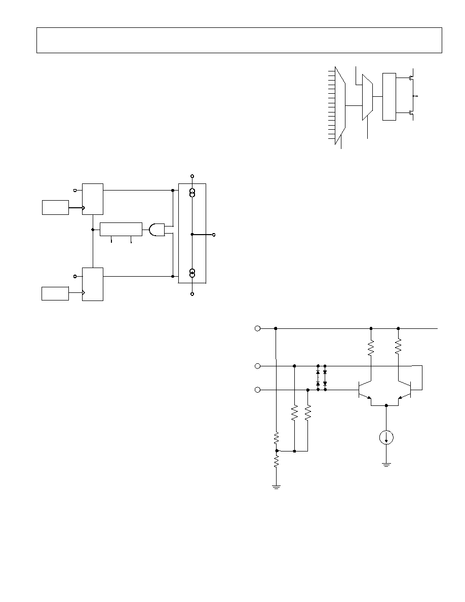
PHASE FREQUENCY DETECTOR (PFD) AND
CHARGE PUMP
The PFD takes inputs from the R counter and N counter
(N = BP + A) and produces an output proportional to the phase
and frequency difference between them. Figure 14 is a
simplified schematic. The PFD includes a programmable delay
element that controls the width of the antibacklash pulse. This
pulse ensures that there is no dead zone in the PFD transfer
function and minimizes phase noise and reference spurs. Two
bits in Register 0D <1:0> control the width of the pulse.
HI
HI
D1
D2
Q1
Q2
CLR1
CLR2
CP
U1
U2
UP
DOWN
GND
U3
R DIVIDER
PROGRAMMABLE
DELAY
N DIVIDER
V
P
CHARGE
PUMP
Antibacklash
pulse width
Figure 14. PFD Simplified Schematic and Timing (In Lock)
STATUS PIN
The output multiplexer on the AD9510 allows access to various
internal points on the chip. The state of the STATUS pin is
controlled by Register 08 <5:2>. Figure 15 shows the STATUS
pin section in block diagram form.
Lock Detect
The STATUS pin can be programmed for two types of lock
detect: digital and analog.
See Table 20 OD <5> for the description of this function.
The N-channel, open-drain, analog lock detect should be
operated with an external pull-up resistor of 30 k nominal.
When lock is detected, the output is high with narrow, low
going pulses.
Off (low) (default)
Digital Lock Detec (active high)
N Divider Output
Digital Lock Detec (active low)
R Divider Output
Analog Lock Detec (n-channel open drain)
A Counter Output
Prescaler Outpu (NCLK)
PFD U Pulse
PFD Down Pulse
Loss o Reference (active high)
TriState
Analog Lock Detec (p-channel open drain)
Loss o reference or Lock Detec (active high)
Loss o reference or Lock Detec (active low)
Loss o Reference (active low)
Sync Detect
PLL MUX CONTROL
08h <5:2>
SYNC DETECT ENABLE
58h <0>
STATUS
pin
GND
V
S
c
o
n
t
r
o
l
f
o
r
a
n
a
l
o
g
l
o
c
k
d
e
t
e
c
t
m
o
d
e
Figure 15. STATUS Pin Circuit
CLK1 CLOCK INPUT
CLK1 is the distribution only clock input. This clock input is
selected by default on power-up. It is usable for inputs up to
1500 MHz.
CLK2 is electrically identical but feeds the PLL N divider as well
as being selectable as the input for the distribution section
through the clock select MUX.
If the distribution section is being used only, it is recommended
that the unselected clock input be powered down in order to
eliminate any possibility of unwanted crosstalk between the
selected clock input and the unselected clock input.
2.5k
2.5k
5k
5k
Clock input
stage
VS
CLK
CLKB
Figure 16. CLK1, CLK2 Equivalent Input Circuit
AD9510
Preliminary Technical Data
Rev. PrA | Page 24 of 41
SERIAL CONTROL PORT
The AD9510 serial control port is a flexible, synchronous, serial
communications port that allows an easy interface with many
industry-standard microcontrollers and microprocessors. The
AD9510 serial control port is compatible with most
synchronous transfer formats, including both the Motorola SPI®
and Intel® SSR protocols. The serial control port allows
read/write access to all registers that configure the AD9510.
Single or multiple byte transfers are supported, as well as MSB
first or LSB first transfer formats. The AD9510 serial control
port can be configured for single pin I/O (SDIO only) or two
unidirectional pins for in/out (SDIO/SDO).
SERIAL CONTROL PORT PIN DESCRIPTIONS
SCLK
(serial clock) is the serial shift clock. This pin is an input.
SCLK is used to synchronize serial control port reads and
writes. Write data bits are registered on the rising edge of this
clock, and read data bits are registered on the falling edge. This
pin is internally pulled down by a 30 k resistor to ground.
SDIO
(serial data input/output) is a dual-purpose pin and acts
as either an input only in 4-wire mode or as an input/output in
3-wire mode. The AD9510 defaults to 3-wire mode (single pin
I/O--SDIO only). Four-wire mode (two unidirectional pins for
I/O SDIO/SDO) may be enabled by setting 1 into the SDO
enable register at Address 00h, Bit <7>.
SDO
(serial data out) is used in the 4-wire mode only as a
separate output pin for readback data. The AD9510 defaults to
3-wire mode. Four-wire mode may be enabled by setting 1 into
the SDO enable register at Address 00h, Bit <7>.
CSB
(chip select bar) is an active low control that gates the read
and write cycles. When CSB is high, SDO and SDIO are in a
high impedance state. This pin is internally pulled down by a
30 k resistor to ground.
SD0 (pin 20)
SCLK (pin 18)
SDI0 (pin 19)
CSB (pin 21)
AD9510
SERIAL
CONTROL
PORT
Figure 17. Serial Control Port
GENERAL OPERATION OF SERIAL CONTROL PORT
There are three phases to a communication cycle with the
AD9510. Phase 1 is the instruction cycle, which is the writing of
a 16-bit instruction word into the AD9510, coincident with the
first 16 SCLK rising edges. The instruction word provides the
AD9510 serial control port with information regarding the data
transfer cycle (Phase 2) of the communication cycle. The
Phase 1 instruction word defines whether the upcoming data
transfer is read or write, the number of bytes in the data
transfer, and the starting register address for the first byte of the
data transfer.
Write
If the instruction word (Phase 1) is for a write operation
(I15 = 0), then Phase 2 is the transfer of data into the serial
control port buffer of the AD9510. The length of the transfer (1,
2, 3, or 4 data bytes) is indicated by 2 bits (W1:W0) in the
instruction byte. Multibyte data transfer is the preferred
method. Single byte data transfers are useful to reduce CPU
overhead when only one byte of data needs to be loaded. CSB
can be raised after each sequence of 8 bits (except the last byte)
to stall the bus. The serial transfer resumes when CSB is
lowered. Stalling on nonbyte boundaries resets the serial control
port.
Since data is written into a serial control port buffer area, not
directly into the AD9510's actual control registers, a Phase 3
operation is needed in order to transfer the serial control port
buffer contents to the actual control registers of the AD9510,
thereby causing them to take effect. Phase 3 consists of writing a
high bit (one) to Address 5Ah, Bit <0>. This update bit is self-
clearing (it is not required to write a 0 to it in order to clear it).
Since any number of bytes of data may be changed before
issuing an update, the update simultaneously enables all register
changes since any previous update.
Read
If the instruction word (Phase 1) is for a read operation
(I15 = 1), the next N × 8 SCLK cycles clock out the data from
the address specified in the instruction word, where N is 1 to 4
as determined by W1:W0. The readback data is valid on the
falling edge of SCLK.
The default mode of the AD9510 serial control port is 3-wire
mode; therefore, the requested data normally appears on the
SDIO pin. It is possible to set the AD9510 to 4-wire mode by
setting 1 into the SDO enable register at Address 00h, Bit <7>.
In 4-wire mode, the readback data appears on the SDO pin.
A readback request reads the data that is in the serial control
port buffer area not the active data in the AD9510's actual
control registers.
SCLK
SDIO
SDO
CSB
SERIAL
CONTROL
PORT
AD9510 CORE
R
E
G
I
S
T
E
R
B
U
F
F
E
R
S
C
O
N
T
R
O
L
R
E
G
I
S
T
E
R
S
* UPDATE
REGISTERS
5Ah <0>
Figure 18. Relationship between Serial Control Port Register Buffers and
Control Registers of the AD9510
Preliminary Technical Data
AD9510
Rev. PrA | Page 25 of 41
The AD9510 uses Addresses 00h to 5Ah. Although the AD9510
serial control port allows for both 8-bit and 16-bit instructions,
the 8-bit instruction mode provides access only to five address
bits (A4 to A0), which restricts its use to the address space 00h
to 01F. The AD9510 defaults to 16-bit instruction mode on
power-up. The 8-bit instruction mode (although defined for
this serial control port) is not useful for the AD9510; therefore,
it is not discussed in this data sheet.
THE INSTRUCTION WORD (16 BITS)
The MSB of the instruction word is
R/W
, which indicates
whether the instruction will be a read or a write. The next two
bits, W1:W0, indicate the length of the transfer in bytes. The
final 13 bits are the address (A12:A0) at which to begin the read
or write operation. For a write, the instruction word is followed
by the number of bytes of data indicated by Bits W1:W0, which
is interpreted according to Table 17.
Table 17. Byte Transfer Count
W1 W0 Bytes
to
Transfer
0 0 1
0 1 2
1 0 3
1 1 4
A12:A0
: These 13 bits select the address within the register map
which is written to or read from during the data transfer
portion of the communications cycle. For multibyte transfers,
this address is the starting byte address. In MSB first mode,
subsequent bytes increment the address.
MSB/LSB FIRST TRANSFERS
The AD9510 instruction word and byte data may be MSB first
or LSB first. The default for the AD9510 is MSB first. The LSB
first mode may be set by writing 1 to Address 00h, Bit <6>. This
takes effect immediately (since it only affects the operation of
the serial control port) and does not require that an update be
executed. Immediately after the LSB first bit is set, all serial
control port operations are changed to LSB first order.
When MSB first mode is active, the instruction and data bytes
must be written from MSB to LSB. Multibyte data transfers in
MSB first format start with an instruction byte that includes the
register address of the most significant data byte. Subsequent
data bytes must follow in order from high address to low
address. In MSB first mode, the serial control port internal byte
address generator decrements for each data byte of the
multibyte transfer cycle.
When LSB_First = 1 (LSB first), the instruction and data bytes
must be written from LSB to MSB. Multibyte data transfers in
LSB first format start with an instruction byte that includes the
register address of the least significant data byte followed by
multiple data bytes. The serial control port internal byte address
generator increments for each byte of the multibyte transfer
cycle.
The AD9510 serial control port data address decrements from
the data address written toward 0x00 for multibyte I/O
operations if the MSB first mode is active. The serial control
port address increments from the data address written toward
0x1F for multibyte I/O operations if the LSB first mode is
active.
Table 18. Serial Control Port, 16-Bit Instruction Word, MSB First
MSB
LSB
I15 I14 I13 I12 I11 I10 I9 I8 I7 I6 I5 I4 I3 I2 I1 I0
R/W
W1 W0 A12 A11 A10 A9 A8 A7 A6 A5 A4 A3 A2 A1 A0
AD9510
Preliminary Technical Data
Rev. PrA | Page 26 of 41
CSB
SDIO
W0 A11 A11 A10 A9 A8
A7 A6
A5
A4
A3 A2
A1
A0
R/W
W1
DON'T CARE
DON'T CARE
16 BIT INSTRUCTION HEADER
D6
D5
D4
D3
D2
D1
D0
SCLK
DON'T CARE
DON'T CARE
D7
D6
D5
D4
D3 D2
D1
D0
D7
REGISTER (N) DATA
REGISTER (N-1) DATA
Figure 19. Serial Control Port Write--MSB First, 16-Bit Instruction, 2 Bytes Data
CSB
SCLK
SDIO
DON'T CARE
W0 A11 A11 A10 A9 A8
A7 A6
A5
A4
A3
A2
A1
A0
R/W
W1
DON'T CARE
DON'T CARE
DON'T CARE
16 BIT INSTRUCTION HEADER
REGISTER (N) DATA
REGISTER (N-1) DATA
REGISTER (N-2) DATA
REGISTER (N-3) DATA
SDO
DON'T CARE
DON'T CARE
D7 D6
D5
D4
D3
D2
D1
D0
D7 D6
D5
D4
D3
D2
D1
D0
D7 D6
D5
D4
D3
D2
D1
D0
D7 D6
D5
D4
D3
D2
D1
D0
Figure 20. Serial Control Port Read--MSB First, 16-Bit Instruction, 4 Bytes Data
t
S
t
DS
t
DH
t
HI
t
LO
t
CLK
t
H
DON'T CARE
DON'T CARE
W1
W0
A12
A11
A10
A9
A8
A7
A6
A5
D4
D3
D2
D1
D0
DON'T CARE
DON'T CARE
CSB
SCLK
SDIO
R/W
Figure 21. Serial Control Port Write-MSB First, 16-Bit Instruction, Timing Measurements
DATA BIT n1
DATA BIT n
CSB
SCLK
SDIO
SDO
03152-P
r
D-007
t
DV
Figure 22. Timing Diagram for Serial Control Port Register Read
CSB
SDIO
W0
A12
A11
A10
A9
A8
A7
A6
A5
A4
A3
A2
A1
A0
R/W
W1
DON'T CARE
DON'T CARE
16 BIT INSTRUCTION HEADER
D6
D5
D4
D3
D2
D1
D0
SCLK
DON'T CARE
DON'T CARE
D7
D6
D5
D4
D3
D2
D1
D0
D7
REGISTER (N) DATA
REGISTER (N+1) DATA
Figure 23. Serial Control Port Write--LSB First, 16-Bit Instruction, 2 Bytes Data
Preliminary Technical Data
AD9510
Rev. PrA | Page 27 of 41
REGISTER MAP AND DESCRIPTION
SUMMARY TABLE
Table 19. AD9510 Register Map
Addr
(Hex)
Parameter
Name
Bit 7
(MSB)
Bit 6
Bit 5
Bit 4
Bit 3
Bit 2
Bit 1
Bit 0
(LSB)
Def.
Value
(Hex) Notes
00
Serial
Control Port
Configuration
SDO
Active
LSB
First
Soft
Reset
Long_Ins Long_Ins
Soft
Reset
LSB
First
SDO
Active
10
<7:4>
Mirror
<3:0>
01
Blank
02
Reserved
03
Blank
PLL
PLL Starts
in Power-
Down
04
A Counter
Blank
6-Bit A Counter <5:0>
00
N Divider
(A)
05
B Counter
Blank
13-Bit B Counter Bits (MSB) 12:8 <4:0>
00
N Divider
(B)
06
B Counter
13-Bit B Counter Bits 7:0 (LSB) <7:0>
00
N Divider
(B)
07
PLL 1
Reserved
LOR lock_del <6:5>
LOR Mode <4:3>
LOR
Enable
Test Test
00
08 PLL
2
Reserved
PFD
Polarity
PLL Mux Select <5:2>
CP Mode <1:0>
00
09
PLL 3
Reserved
CP Current <6:4>
Reserved
Reset R
Counter
Reset N
Counter
Reset All
Counters
00
0A PLL
4
Reserved B
Bypass
Reserved
Prescaler P <4:2>
Power-Down <1:0>
01
N Divider
(P)
0B
R Divider
Blank
14-Bit R Divider Bits (MSB) 13:8 <5:0>
00
R Divider
0C
R Divider
14-Bit R Divider Bits (MSB) 13:8 <5:0>
00
R Divider
0D PLL
5
Reserved
Digital
Lock
Det.
Enable
Digital
Lock
Det.
Window
Reserved
Antibacklash Pulse-
Width <1:0>
00
OE-
33
Blank
FINE DELAY
ADJUST
Fine
Delays
Bypassed
34
Delay Bypass 5
Blank
Bypass
01
Bypass
Delay
35
Delay Full-
Scale 5
Blank
Ramp Capacitor <5:3>
Ramp Current <2:0>
00
Max. Delay
Full-Scale
36
Delay Word 5
Blank
6-Bit Delay Word <5:0>
00
Min. Delay
Value
37
Delay FS
Adjust 5
Blank
I Adjust for Process <2:0>
04
Midpoint
38
Delay Bypass 6
Blank
Bypass
01
Bypass
Delay
39
Delay Full-
Scale 6
Blank
Ramp Capacitor <5:3>
Ramp Current <2:0>
00
Max. Delay
Full-Scale
3A
Delay Word 6
Blank
6-Bit Delay Word <5:0>
00
Min. Delay
Value
AD9510
Preliminary Technical Data
Rev. PrA | Page 28 of 41
Addr
(Hex)
Parameter
Name
Bit 7
(MSB)
Bit 6
Bit 5
Bit 4
Bit 3
Bit 2
Bit 1
Bit 0
(LSB)
Def.
Value
(Hex) Notes
3B
Delay FS
Adjust 6
Blank
I Adjust for Process <2:0>
04
Midpoint
OUTPUTS
3C
LVPECL OUT0
Blank
Output Level <3:2>
Power-Down <1:0>
0A
OFF
3D
LVPECL OUT1
Blank
Output Level <3:2>
Power-Down <1:0>
08
ON
3E
LVPECL OUT2
Blank
Output Level <3:2>
Power-Down <1:0>
08
ON
3F
LVPECL OUT3
Blank
Output Level <3:2>
Power-Down <1:0>
08
ON
40
LVDS_CMOS
OUT 4
Blank
CMOS
Inverted
Driver
On
Logic
Select
Output Level <2:1>
Output
Power
02 LVDS,
ON
41
LVDS_CMOS
OUT 5
Blank
CMOS
Inverted
Driver
On
Logic
Select
Output Level <2:1>
Output
Power
02 LVDS,
ON
42
LVDS_CMOS
OUT 6
Blank
CMOS
Inverted
Driver
On
Logic
Select
Output Level <2:1>
Output
Power
03 LVDS,
OFF
43
LVDS_CMOS
OUT 7
Blank
CMOS
Inverted
Driver
On
Logic
Select
Output Level <2:1>
Output
Power
03 LVDS,
OFF
44
Blank
Test
Test
CLK1 AND
CLK2
Input
Receivers
45
Clocks select,
Power-Down
(PD) Options
Test
CLKs in
PD
REFIN PD
CLK to
PLL PD
CLK2 PD
CLK1
PD
Select
CLK IN
01
All Clocks
ON, Select
CLK1
46,47
Blank
DIVIDERS
48
Divider 0
Low Cycles <7:4>
High Cycles <3:0>
00
Divide by 2
49 Divider
0
Bypass No
Sync
Force
Start H/L
Phase Offset <3:0>
00
Phase = 0
4A
Divider 1
Low Cycles <7:4>
High Cycles <3:0>
00
Divide by 2
4B Divider
1
Bypass No
Sync
Force
Start H/L
Phase Offset <3:0>
00
Phase = 0
4C
Divider 2
Low Cycles <7:4>
High Cycles <3:0>
11
Divide by 4
4D Divider
2
Bypass No
Sync
Force
Start H/L
Phase Offset <3:0>
00
Phase = 0
4E
Divider 3
Low Cycles <7:4>
High Cycles <3:0>
33
Divide by 8
4F Divider
3
Bypass No
Sync
Force
Start H/L
Phase Offset <3:0>
00
Phase = 0
50
Divider 4
Low Cycles <7:4>
High Cycles <3:0>
00
Divide by 2
51 Divider
4
Bypass No
Sync
Force
Start H/L
Phase Offset <3:0>
00
Phase = 0
52
Divider 5
Low Cycles <7:4>
High Cycles <3:0>
11
Divide by 4
53 Divider
5
Bypass No
Sync
Force
Start H/L
Phase Offset <3:0>
00
Phase = 0
54
Divider 6
Low Cycles <7:4>
High Cycles <3:0>
00
Divide by 2
55 Divider
6
Bypass No
Sync
Force
Start H/L
Phase Offset <3:0>
00
Phase = 0
56
Divider 7
Low Cycles <7:4>
High Cycles <3:0>
00
Divide by 2
Preliminary Technical Data
AD9510
Rev. PrA | Page 29 of 41
Addr
(Hex)
Parameter
Name
Bit 7
(MSB)
Bit 6
Bit 5
Bit 4
Bit 3
Bit 2
Bit 1
Bit 0
(LSB)
Def.
Value
(Hex) Notes
57 Divider
7
Bypass No
Sync
Force
Start H/L
Phase Offset <3:0>
00
Phase = 0
FUNCTION
58
FUNCTION
Pin and Sync
Reserved
Set FUNCTION Pin
PD Sync
PD All
Ref.
Sync
Reg.
Sync
Select
Sync
Enable
00
FUNCTION
Pin =
RESETB
59
Reserved
5A
Update
Registers
Blank
Update
Registers
00
Self-
Clearing
Bit
END
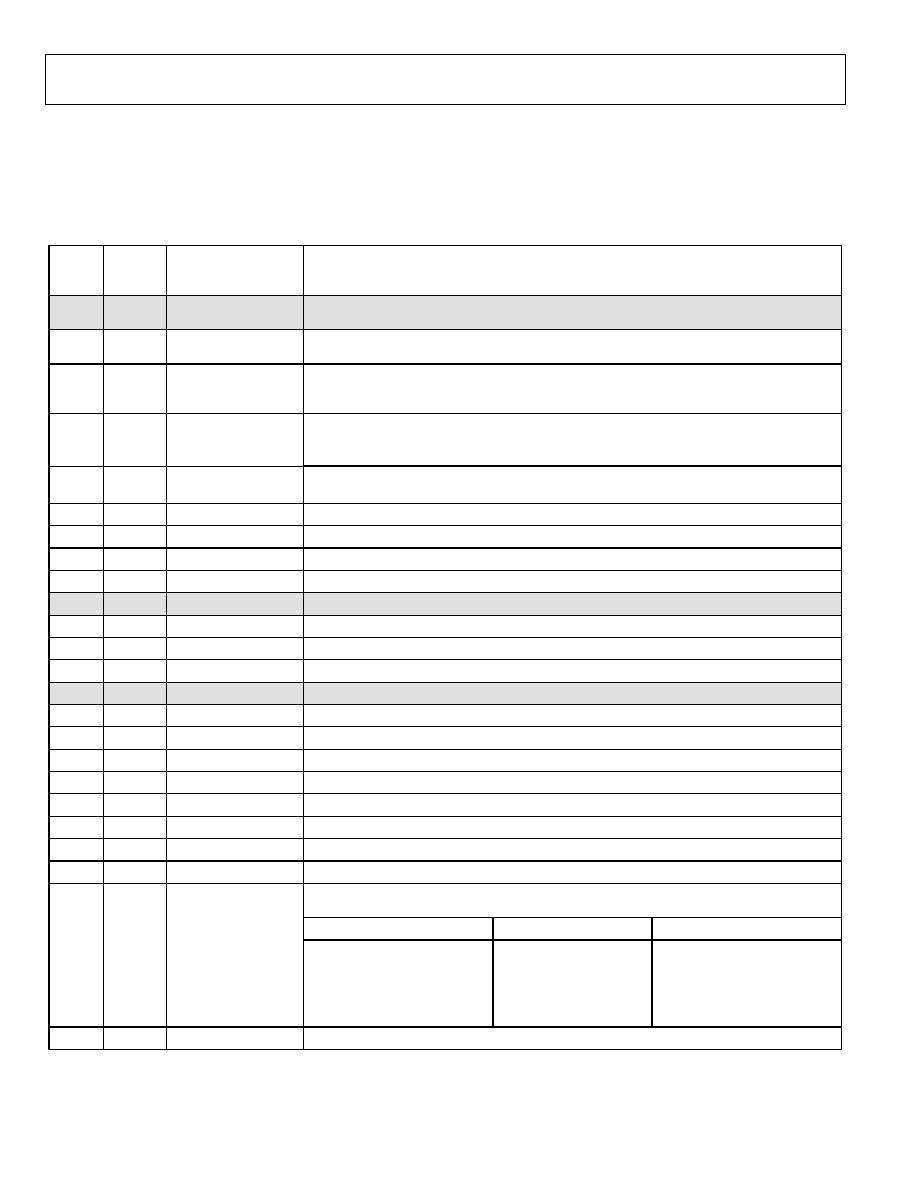
AD9510
Preliminary Technical Data
Rev. PrA | Page 30 of 41
REGISTER MAP DESCRIPTION
The is a detailed description of each of the control register functions. The registers are listed by hexadecimal address. Reference to a
specific bit or range of bits within a register is accomplished by the use of angle brackets. For example, <3> refers to Bit 3, while <5:2>
refers to the range of bits from Bit 5 through Bit 2. Table 20 describes the functionality of the control registers on a bit-by-bit basis. For a
more concise (but less descriptive) table see Table 19.
Table 20. AD9510 Register Descriptions
Reg.
Addr.
(Hex) Bit(s) Name
Description
Serial Control Port
Configuration
Note: <7:4> mirror <3:0> to ensure that this register can be accessed regardless of the state of
<1> or <6> (the bit that sets LSB first).
00 <0> SDO
Active
When set causes SDO to become active. When clear, the SDO pin remains in tri-state and all
read data is routed to the SDIO pin. (Default = 0.)
00 <1> LSB
First
When set causes input and output data to be oriented as LSB first. Additionally, addressing
increments. If this bit is clear, data is oriented as MSB first and addressing decrements. (Default
= 0, MSB first.)
00 <2> Soft
Reset
When a 1 is written to this bit, the chip executes a soft reset, restoring default values to all of
the internal registers.
This bit is self-clearing. A 0 does not have to be written to clear it.
00
<3>
Long Instruction
When set, the instruction phase is 16 bits. When clear, the instruction phase is 8 bits.
The default, and only, mode for this part is long instruction. (Default = 1.)
00
<4>
Long Instruction
Same as <3>.
00
<5>
Soft Reset
Same as <2>.
00
<6>
LSB First
Same as <1>.
00
<7>
SDO Active
Same as <0>.
Unused
01
<7:0>
Reserved or not used.
02
<7:0>
Reserved or not used.
03
<7:0>
Reserved or not used.
PLL Settings
04
<5:0>
A Counter
6-bit A counter <5:0>.
04
<7:6>
Reserved or not used.
05
<4:0>
B Counter MSBs
13-bit B counter (MSB) <12:8>.
05
<7:5>
Reserved or not used.
06
<7:0>
B Counter LSBs
13-bit B counter (LSB) <7:0>.
07
<1:0>
Reserved or not used.
07
<2>
LOR Enable
1 = enables the loss of reference (LOR) function; (Default = 0).
07
<4:3>
Reserved or not used (default = 00).
07 <6:5>
LOR Initial Lock Detect
Delay
LOR initial lock detect delay. Once a lock detect is indicated, this is the number of phase
frequency detector (PFD) cycles that occur prior to turning on the LOR monitor.
<6>
<5>
LOR Initial Lock Deteck Delay
0
0
3 PFD Cycles (Default)
0
1
6 PFD Cycles
1
0
12 PFD Cycles
1
1
24 PFD Cycles
07
<7>
Reserved or not used
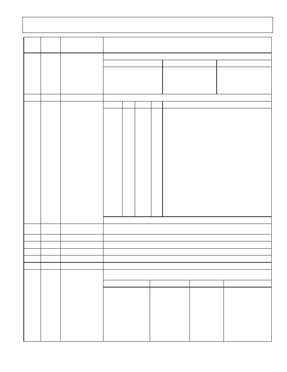
Preliminary Technical Data
AD9510
Rev. PrA | Page 31 of 41
Reg.
Addr.
(Hex) Bit(s) Name
Description
08
<1:0>
Charge Pump Mode
<1>
<0>
Charge Pump Mode
0
0
Tri-Stated
(Default)
0
1
Pump
Up
1
0
Pump
Down
1
1
Normal
Operation
08
<5:2>
PLL Mux Control
<5> <4>
<3>
<2>
MUXOUT
0
0
0
0
Off (Signal Goes Low) (Default)
0
0
0
1
Digital Lock Detect (Active High)
0
0
1
0
N Divider Output
0
0
1
1
Digital Lock Detect (Active High)
0
1
0
0
R Divider Output
0
1
0
1
Analog Lock Detect (N Channel Open-Drain)
0
1
1
0
A Counter Output
0 1
1
1
Prescaler
Output
(NCLK)
1
0
0
0
PFD Up Pulse
1
0
0
1
PFD Down Pulse
1
0
1
0
Loss of Reference (Active High)
1 0
1
1
Tri-State
1
1
0
0
Analog Lock Detect (P Channel Open-Drain)
1
1
0
1
Loss of Reference or Lock Detect (Active High)
1
1
1
0
Loss of Reference or Lock Detect (Active Low)
1
1
1
1
Loss of Reference (Active High)
MUXOUT is the PLL portion of the STATUS Output MUX.
08 <6> Phase-Frequency
Detector (PFD) Polarity
0 = negative (default), 1 = positive.
08
<7>
Reserved or not used.
09
<0>
Reset All Counters
0 = normal (default), 1 = reset R, A, and B counters.
09
<1>
N-Counter Reset
0 = normal (default), 1 = reset A and B counters.
09
<2>
R-Counter Reset
0 = normal (default), 1 = reset R counter.
09
<3>
Reserved or not used.
09 <6:4>
Charge Pump (CP)
Current Setting
<6> <5>
<4>
I
CP
(mA)
0
0
0
0.62
0
0
1
1.25
0
1
0
1.87
0
1
1
2.50
1
0
0
3.12
1
0
1
3.75
1
1
0
4.37
1
1
1
5.00
AD9510
Preliminary Technical Data
Rev. PrA | Page 32 of 41
Reg.
Addr.
(Hex) Bit(s) Name
Description
Default = 000.
These currents assume: CP_RSET = 5.1 k.
Actual current can be calculated by: CP_lsb = 3.1875/CP_RSET.
09
<7>
Reserved or not used.
0A
<1:0>
PLL Power-Down
01 = asynchronous power-down (default).
<1> <0>
Mode
0
0
Normal
Operation
0
1
Asynchronous
Power-Down
1
0
Normal
Operation
1
1
Synchronous
Power-Down
0A <4:2>
Prescaler
Value
P/P+1
<4> <3>
<2>
Mode
Prescaler
Mode
0 0
0
FD
Divide-by-1
0 0
1
FD
Divide-by-2
0 1
0
DM
2/3
0 1
1
DM
4/5
1 0
0
DM
8/9
1 0
1
DM
16/17
1 1
0
DM
32/33
1 1
1
FD
Divide-by-3
DM = Dual Modulus, FD = Fixed Divide.
0A
<5>
Reserved or not used.
0A
<6>
B Counter Bypass
Only valid when operating the prescaler in fixed divide (FD) mode. When this bit is set, the B
counter is divide-by-1. This allows the prescaler setting to determine the divide for the N
divider.
0A
<7>
Reserved or not used.
0B <5:0>
14-Bit Reference
Counter, MSBs
R divider (MSB) <13:8>.
0C <7:0>
14-Bit Reference
Counter, R LSBs
R divider (MSB) <7:0>.
0D <1:0>
Antibacklash Pulse-
Width
<1>
<0>
Antibacklash Pulse-Width (ns)
0
0
1.3
(Default)
0
1
2.9
1
0
6.0
1
1
1.3
0D
<4:2>
Reserved or not used.
0D <5> Digital Lock Detect
Window
<5>
Digital Lock Detect Window
(ns)
Digital Lock Detect Loss of Lock Threshold (ns)
0
(Default)
9.5
15
1 3.5
7
Preliminary Technical Data
AD9510
Rev. PrA | Page 33 of 41
Reg.
Addr.
(Hex) Bit(s) Name
Description
If the time difference of the rising edges at the inputs to the PFD are less than the lock detect
window time, the digital lock detect flag is set. The flag remains set until the time difference is
greater than loss-of-lock threshold.
0D
<6>
Lock Detect Disable
0 = normal lock detect operation (default).
1 = disable lock detect.
0D
<7>
Reserved or not used.
Unused
0E-33
Reserved or not used.
Fine Delay Adjust
34
(38)
<0> Delay
Control
OUT5
(OUT6)
Delay block control bit.
Bypasses delay block and powers it down (default = 1).
34
(38)
<7:1>
Reserved or not used.
35
(39)
<2:0> Ramp
Control
OUT5
(OUT6)
The slowest ramp (200 µs) sets the longest full scale of approximately 10 ns.
<2>
<1>
<0>
Ramp Current (µs)
0
0
0
200
0
0
1
400
0
1
0
600
0
1
1
800
1
0
0
1000
1
0
1
1200
1
1
0
1400
1
1
1
1600
35
(39)
<5:3>
Ramp Control
OUT5
(OUT6)
Selects the number of capacitors in ramp generation circuit.
More capacitors => slower ramp.
<5>
<4>
<3>
Number of Capacitors
0
0
0
4
(Default)
0
0
1
3
0
1
0
3
0
1
1
2
1
0
0
3
1
0
1
2
1
1
0
2
1
1
1
1
36
(3A)
<5:0> Reference
Value
OUT5
(OUT6)
Sets delay within full scale of the ramp. There are 64 steps to control the reference value for the
comparator.
000000 => zero delay (default).
111111 => maximum delay.
37
(3B)
<2:0>
Delay Fine Tune
OUT5
(OUT6)
The delay fine tune slightly increases or decreases the ramp current (-8% to +13%) to negate
the process variation of the caps. Defaults to 100, which is the midpoint.
AD9510
Preliminary Technical Data
Rev. PrA | Page 34 of 41
Reg.
Addr.
(Hex) Bit(s) Name
Description
3C
(3D)
(3E)
(3F)
<1:0>
Power Down
LVPECL
OUT0
(OUT1)
(OUT2)
(OUT3)
Mode
<1> <0> Description
Output
ON
0 0 Normal
operation
ON
PD1
0
1
Test only--do not
use
OFF
PD2
1 0 Safe
power-down
Partial power-
down; use if
output has load
resistors
OFF
PD3
1
1
Total power-
down
Use only if output
has no load
resistors
OFF
3C
(3D)
(3E)
(3F)
<3:2>
Output Level
LVPECL
OUT0
(OUT1)
(OUT2)
(OUT3)
This sets output single-ended voltage levels for LVPECL outputs
<3>
<2>
Output Voltage (mV)
0
0
490
0
1
330
1
0
805
(Default)
1
1
650
3C
(3D)
(3E)
(3F)
<7:4>
Reserved or not used.
40
(41)
(42)
(43)
<0> Power-Down
LVDS/CMOS
OUT4
(OUT5)
(OUT6)
(OUT7)
Power-down bit for both output and LVDS driver.
0 = LVDS/CMOS on (default).
1 = LVDS/CMOS power-down.
40
(41)
(42)
(43)
<2:1>
Output Current Level
LVDS
OUT4
(OUT5)
(OUT6)
(OUT7)
Preliminary Technical Data
AD9510
Rev. PrA | Page 35 of 41
Reg.
Addr.
(Hex) Bit(s) Name
Description
<2>
<1>
Current (mA)
Termination ()
0
0
1.75
100
0
1
3.5
(Default) 100
1
0
5.25
50
1 1 7 50
40
(41)
(42)
(43)
<3> LVDS/CMOS
Select
OUT4
(OUT5)
(OUT6)
(OUT7)
0 = LVDS (default).
1 = CMOS.
40
(41)
(42)
(43)
<4> Inverted
CMOS
Driver
OUT4
(OUT5)
(OUT6)
(OUT7)
Affects output only when in CMOS mode.
0 = disable inverted CMOS driver (default).
1 = enable inverted CMOS driver.
40
(41)
(42)
(43)
<7:5>
Reserved or not used.
44
<7:0>
Reserved or not used.
45
<0>
Clock Select
0: CLK2 drives distribution section.
1: CLK1 drives distribution section (default).
45
<1>
CLK1 Power-Down
1 = CLK1 input is powered down (default = 0).
45
<2>
CLK2 Power-Down
1 = CLK2 input is powered down (default = 0).
45 <3> Prescaler Clock Power-
Down
1 = shut down clock signal to PLL prescaler (default = 0).
45
<4>
REFIN Power-Down
1 = power-down REFIN (default = 0).
45 <5> All Clock Inputs Power-
Down
1 = power-down CLK1 and CLK2 inputs and associated bias and internal clock tree;
(default = 0).
45
<7:6>
Reserved or not used.
46
<7:0>
Reserved or not used.
47
<7:0>
Reserved or not used.
48
(4A)
(4C)
(4E)
(50)
(52)
(54)
(56)
<3:0> Divider
High
OUT0
(OUT1)
(OUT2)
(OUT3)
(OUT4)
(OUT5)
(OUT6)
(OUT7)
Number of clock cycles divider output stays high.

AD9510
Preliminary Technical Data
Rev. PrA | Page 36 of 41
Reg.
Addr.
(Hex) Bit(s) Name
Description
48
(4A)
(4C)
(4E)
(50)
(52)
(54)
(56)
<7:4> Divider
Low
OUT0
(OUT1)
(OUT2)
(OUT3)
(OUT4)
(OUT5)
(OUT6)
(OUT7)
Number of clock cycles divider output stays low.
49
(4B)
(4D)
(4F)
(51)
(53)
(55)
(57)
<3:0> Phase
Offset
OUT0
(OUT1)
(OUT2)
(OUT3)
(OUT4)
(OUT5)
(OUT6)
(OUT7)
Phase offset (default = 0000).
49
(4B)
(4D)
(4F)
(51)
(53)
(55)
(57)
<4> Start
OUT0
(OUT1)
(OUT2)
(OUT3)
(OUT4)
(OUT5)
(OUT6)
(OUT7)
Selects start high or start low.
(Default = 0).
49
(4B)
(4D)
(4F)
(51)
(53)
(55)
(57)
<5> Force
OUT0
(OUT1)
(OUT2)
(OUT3)
(OUT4)
(OUT5)
(OUT6)
(OUT7)
Forces individual outputs to the state specified in start (above).
This function requires that Nosync (below) also be set.
(Default = 0).
49
(4B)
(4D)
(4F)
(51)
(53)
(55)
(57)
<6> Nosync
OUT0
(OUT1)
(OUT2)
(OUT3)
(OUT4)
(OUT5)
(OUT6)
(OUT7)
Ignore chip-level sync signal (default = 0).
Preliminary Technical Data
AD9510
Rev. PrA | Page 37 of 41
Reg.
Addr.
(Hex) Bit(s) Name
Description
49
(4B)
(4D)
(4F)
(51)
(53)
(55)
(57)
<7> Bypass
Divider
OUT0
(OUT1)
(OUT2)
(OUT3)
(OUT4)
(OUT5)
(OUT6)
(OUT7)
Bypass and power-down divider logic; route clock directly to output (default = 0).
Other
58
<0>
SYNC Detect Enable
1 = enable SYNC detect (default = 0).
58
<1>
SYNC Select
1 = raise flag if slow clocks are out-of-sync by 0.5 to 1 high speed clock cycles.
0 (default) = raise flag if slow clocks are out-of-sync by 1 to 1.5 high speed clock cycles.
58 <2> Soft
SYNC
Soft SYNC bit works the same as the FUNCTION pin when in SYNCB mode, except that this bit's
polarity is reversed. That is a High level forces selected outputs into a known state, and a High
> Low transition triggers a sync (default = 0).
58
<3>
Dist Ref Power Down
1 = power-down the references for the distribution section (default = 0).
58
<4>
SYNC Power Down
1 = power-down the SYNC (default = 0).
58 <6:5>
FUNCTION
Pin Select
<6> <5> Function
0
0
RESETB
(Default)
0
1
SYNCB
1
0
Test Only; Do Not Use
1
1
PDB
58
<7>
Reserved or not used.
59
<7:0>
Reserved or not used.
5A <0> Update
Registers A 1 written to this bit updates all registers and transfers all serial control port register buffer
contents to the control registers on next rising SCLK edge. This is a self-clearing bit. A 0 does
not have to be written in order to clear it.
5A
<7:1>
Reserved or not used.
END
AD9510
Preliminary Technical Data
Rev. PrA | Page 38 of 41
APPLICATIONS
USING THE AD9510 OUTPUTS FOR ADC CLOCK
APPLICATIONS
Any high speed analog-to-digital converter (ADC) is extremely
sensitive to the quality of the sampling clock provided by the
user. An ADC can be thought of as a sampling mixer; and any
noise, distortion, or timing jitter on the clock is combined with
the desired signal at the A/D output. Clock integrity
requirements scale with the analog input frequency and
resolution, with higher analog input frequency applications at
>= 14-bit resolution being the most stringent. The theoretical
SNR of an ADC is limited by the ADC resolution and the jitter
on the sampling clock. Considering an ideal ADC of infinite
resolution where the step size and quantization error can be
ignored, the available SNR is can be expressed approximately by
×
=
J
ft
SNR
2
1
log
20
where f is the highest analog frequency being digitized, and t
j
is
the rms jitter on the sampling clock. The figure below shows
required sampling clock jitter as function of analog frequency
and effective number of bits (ENOB)
Figure 24. ENOB and SNR vs. Analog Input Frequency
(See Application Note AN-501 at www.analog.com for more
information).
Many high performance ADC's feature differential clock inputs
to simplify the task of providing the required low jitter clock on
a noisy PCB. (Distributing a single-ended clock on a noisy PCB
can result in coupled noise on the sample clock. Differential
distribution has inherent common-mode rejection that can
provide superior clock performance in a noisy environment.) The
AD9510 features both LVPECL and LVDS outputs that provide
differential clock outputs, which enable clock solutions that
maximize converter SNR performance. The input requirements
of the ADC (differential or single-ended, logic level,
termination) should be considered when selecting the best
clocking/converter solution.
CMOS CLOCK DISTRIBUTION
The AD9510 provides four clock outputs (OUT4 to OUT7)
which are selectable as either CMOS or LVDS levels. When
selected as CMOS, these outputs provide a way to drive devices
requiring CMOS level logic at their clock inputs. Due to factors
inherent to CMOS logic, the jitter performance of these outputs
cannot equal that of the LVPECL and LVDS outputs. However,
for many clocking needs within a system, CMOS clock levels are
appropriate.
Whenever single-ended CMOS clocking is used, some of the
following general guidelines should be followed.
Point-to-point nets should be designed such that a driver only
has one receiver on the net, if possible. This allows for simple
termination schemes and minimize ringing due to possible
mismatched impedances on the net. Series termination at the
source is generally required to provide transmission line
matching and/or to reduce current transients at the driver. The
value of the resistor is dependent on board design and timing
requirements (typically 10 to 100 is used). CMOS outputs
are also limited in terms of the capacitive load or trace length
that they can drive, typically trace lengths less than 3 inches are
recommended to preserve signal rise/fall times and preserve
signal integrity. Simulation results for the AD9510 CMOS
outputs with a 1-inch and 3-inch trace load are shown in
Figure 26. In this example, the series resistor is 10 and the
trace impedance is 60 . Signal integrity, in this example, has
started to degrade already at a 3-inch trace length.
Figure 25. Series Termination of CMOS Output
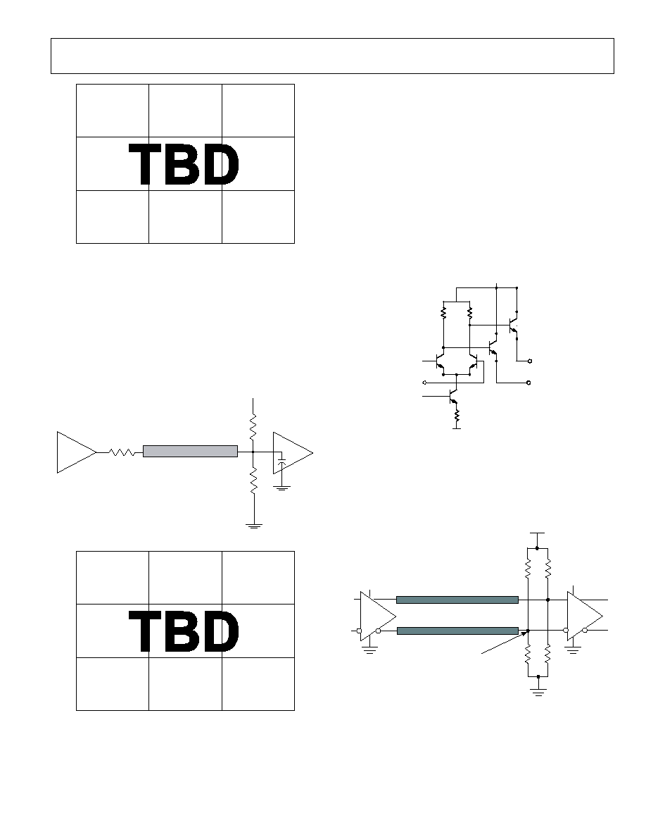
Preliminary Technical Data
AD9510
Rev. PrA | Page 39 of 41
Figure 26. CMOS Output Waveforms
Termination at the far end of the PCB trace is a second option.
The CMOS outputs of the AD9510 do not supply enough
current to provide a full voltage swing with a low impedance
resistive, far-end termination, as shown in Figure 28. The far
end termination network should match the PCB trace
impedance and provide the desired switching point. The
reduced signal swing may still meet receiver input requirements
in some applications. This can be useful when driving long trace
lengths on less critical nets.
100
3pF
Vpullup=3.3V
CMOS
OUT4, OUT5, OUT6, OUT7
selected as CMOS
100
50
10
Figure 27. CMOS Output with Far-End Termination
Figure 28. Far-End Termination of CMOS Output Waveform
Because of the limitations of single-ended CMOS clocking,
consider using differential outputs when driving high speed
signals over long traces. The AD9510 offers both LVPECL and
LVDS outputs that are better suited for driving long traces
where the inherent noise immunity of differential signaling
provides superior performance for clocking converters.
LVPECL CLOCK DISTRIBUTION
The low voltage positive emitter coupled logic (LVPECL)
outputs of the AD9510 provide the lowest jitter clock signals
available from the AD9510. The LVPECL outputs (because they
are open emitter) require a dc termination to bias the output
transistors. A simplified equivalent circuit in Figure 29 shows
the LVPECL output stage.
Out+
Out-
GND
3.3V
Figure 29. Simplified LVPECL Output Stage
In most applications, a standard LVPECL far-end termination is
recommended, as shown in Figure 30. The resistor network is
designed to match the transmission line impedance (50 ) and
the desired switching threshold (1.3 V). Figure 32 shows a
typical LVPECL clock waveform.
3.3V
3.3V
LVPECL
LVPECL
50
127
50
127
83
83
Vt=Vcc - 1.3V
3.3V
single-ended (notcoupled)
LVPECL
LVPECL
Figure 30. LVPECL Far-End Termination
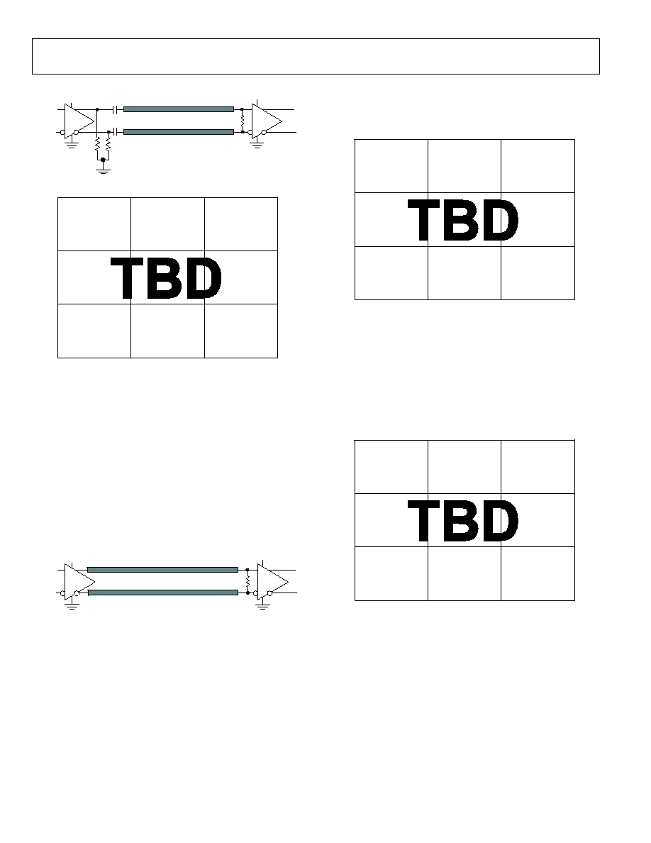
AD9510
Preliminary Technical Data
Rev. PrA | Page 40 of 41
A typical LVDS output waveform is shown in Figure 34.
3.3V
3.3V
LVPECL
LVPECL
100
200
0.1nF
differential (coupled)
200
0.1nF
(See Application Note AN-586 at www.analog.com for more
information on LVDS).
Figure 31 LVPECL with Parallel Transmission Line
Figure 34. Typical LVDS Output Waveforms
POWER AND GROUNDING CONSIDERATIONS,
AND POWER SUPPLY REJECTION
Many applications seek high speed and performance under less
than ideal operating conditions. In these application circuits, the
implementation and construction of the PCB is as important as
the circuit design. Proper RF techniques must be used for device
selection, placement, and routing, as well as power supply
bypassing and grounding to ensure optimum performance.
Figure 32. Typical LVPECL Outputs
LVDS CLOCK DISTRIBUTION
Low voltage differential signaling (LVDS) is a second
differential output option for the AD9510. LVDS provides clock
signals with jitter performance nearly as good as that obtainable
from LVPECL, and better than CMOS. LVDS uses a current-
mode output stage with several user-selectable current levels. A
3.5 mA output current yields 350 mV output swing across a
standard LVDS output termination of 100 , meeting ANSI 644
requirements.
A recommended termination circuit is shown for the LVDS
outputs in Figure 33.
3.3V
3.3V
LVDS
LVDS
100
100
differential (coupled)
LVDS
Figure 35. Differential LC Filter for Single 3.3 V Applications
Figure 33. LVDS Output Termination
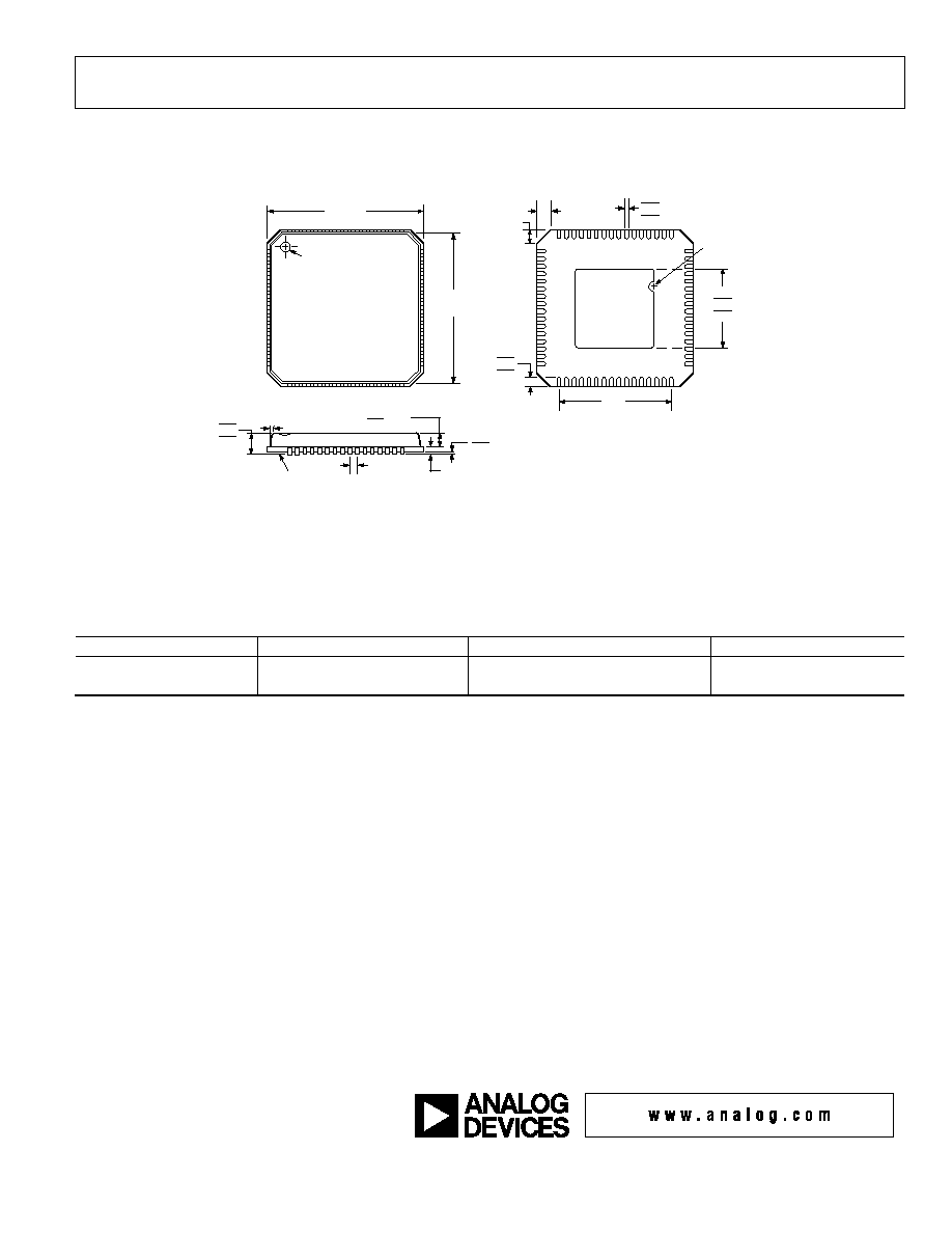
Preliminary Technical Data
AD9510
Rev. PrA | Page 41 of 41
OUTLINE DIMENSIONS
PIN 1
INDICATOR
TOP
VIEW
8.75
BSC SQ
9.00
BSC SQ
1
64
16
17
49
48
32
33
0.45
0.40
0.35
0.50 BSC
0.20 REF
12° MAX
0.80 MAX
0.65 TYP
1.00
0.85
0.80
7.50
REF
0.05 MAX
0.02 NOM
0.60 MAX
0.60 MAX
4.85
4.70 SQ*
4.55
SEATING
PLANE
PIN 1
INDICATOR
EXPOSED PAD
(BOTTOM VIEW)
0.30
0.25
0.18
*COMPLIANT TO JEDEC STANDARDS MO-220-VMMD
EXCEPT FOR EXPOSED PAD DIMENSION
Figure 36. 64-Lead Frame Chip Scale Package [LFCSP]
9 mm × 9 mm Body (CP-64-1)
Dimensions shown in millimeters
ORDERING GUIDE
Model
Temperature Range
Package Description
Package Options
AD9510
-40°C to +85°C
64-Lead Chip Scale Package (LFCSP)
CP-64-1
AD9510PCB
Evaluation
Board
© 2004 Analog Devices, Inc. All rights reserved. Trademarks and
registered trademarks are the property of their respective owners.
PR05046011/04(PrA)
Document Outline
- FEATURES
- APPLICATIONS
- GENERAL DESCRIPTION
- FUNCTIONAL BLOCK DIAGRAM
- TABLE OF CONTENTS
- þÿ
- þÿ
- þÿ
- þÿ
- þÿ
- þÿ
- þÿ
- þÿ
- þÿ
- þÿ
- þÿ
- þÿ