 | ÐлекÑÑоннÑй компоненÑ: AD8113 | СкаÑаÑÑ:  PDF PDF  ZIP ZIP |
Äîêóìåíòàöèÿ è îïèñàíèÿ www.docs.chipfind.ru
REV. A
Information furnished by Analog Devices is believed to be accurate and
reliable. However, no responsibility is assumed by Analog Devices for its
use, nor for any infringements of patents or other rights of third parties that
may result from its use. No license is granted by implication or otherwise
under any patent or patent rights of Analog Devices. Trademarks and
registered trademarks are the property of their respective companies.
a
AD8113
One Technology Way, P.O. Box 9106, Norwood, MA 02062-9106, U.S.A.
Tel: 781/329-4700
www.analog.com
Fax: 781/326-8703 © 2003 Analog Devices, Inc. All rights reserved.
Audio/Video 60 MHz
16 16, G = 2 Crosspoint Switch
FUNCTIONAL BLOCK DIAGRAM
AD8113
OUTPUT
BUFFER
G = +2
80
80
256
80-BIT SHIFT REGISTER
WITH 5-BIT
PARALLEL LOADING
PARALLEL LATCH
DECODE
16 5:16 DECODERS
16
CLK
DATA IN
UPDATE
CE
RESET
16 INPUTS
A0
DATA
OUT
16
OUTPUTS
SET INDIVIDUAL OR
RESET ALL OUTPUTS
TO "OFF"
A1
A2
SER/PAR D0 D1 D2 D3 D4
ENABLE/DISABLE
A3
SWITCH
MATRIX
FEATURES
16 16 High Speed Nonblocking Switch Array
Serial or Parallel Programming of Switch Array
Serial Data Out Allows Daisy Chaining Control of
Multiple 16 16s to Create Larger Switch Arrays
Output Disable Allows Connection of Multiple Devices
without Loading the Output Bus
Complete Solution
Buffered Inputs
16 Output Amplifiers
Operates on 5 V or 12 V Supplies
Low Supply Current of 54 mA
Excellent Audio Performance V
S
= 12 V
10 V Output Swing
0.002% THD @ 20 kHz Max. 20 V p-p (R
L
= 600 )
Excellent Video Performance V
S
= 5 V
10 MHz 0.1 dB Gain Flatness
0.1% Differential Gain Error (R
L
= 1 k )
0.1 Differential Phase Error (R
L
= 1 k )
Excellent AC Performance
3 dB Bandwidth 60 MHz
Low All Hostile Crosstalk of
83 dB @ 20 kHz
Reset Pin Allows Disabling of All Outputs (Connected
to a Capacitor to Ground Provides Power-On
Reset Capability)
100-Lead LQFP (14 mm 14 mm)
APPLICATIONS
Analog/Digital Audio Routers
Video Routers (NTSC, PAL, S-VIDEO, SECAM)
Multimedia Systems
Video Conferencing
CCTV Surveillance
PRODUCT DESCRIPTION
The AD8113 is a fully buffered crosspoint switch matrix that
operates on
±12 V for audio applications and ±5 V for video
applications. It offers a 3 dB signal bandwidth greater than
60 MHz and channel switch times of less than 60 ns with 0.1%
settling for use in both analog and digital audio. The AD8113
operated at 20 kHz has crosstalk performance of 83 dB and
isolation of 90 dB. In addition, ground/power pins surround all
inputs and outputs to provide extra shielding for operation in
the most demanding audio routing applications. The differential
gain and differential phase of better than 0.1% and 0.1
°, respec-
tively, along with 0.1 dB flatness out to 10 MHz, make the
AD8113 suitable for many video applications.
The AD8113 includes 16 independent output buffers that can
be placed into a disabled state for paralleling crosspoint outputs
so that off channel loading is minimized. The AD8113 has a
gain of +2. It operates on voltage supplies of
±5 V or ±12 V
while consuming only 34 mA or 31 mA of current, respectively.
The channel switching is performed via a serial digital control
(which can accommodate daisy-chaining of several devices) or
via a parallel control, allowing updating of an individual output
without reprogramming the entire array.
The AD8113 is packaged in a 100-lead LQFP and is available
over the commercial temperature range of 0
°C to 70°C.

AD8113SPECIFICATIONS
REV. A
Parameter
Conditions
Min
Typ
Max
Unit
DYNAMIC PERFORMANCE
3 dB Bandwidth
V
OUT
= 200 mV p-p, R
L
= 600
, V
S
=
±12 V
46
60
MHz
V
OUT
= 200 mV p-p, R
L
= 150
, V
S
=
±5 V
41
60
MHz
V
OUT
= 8 V p-p, R
L
= 600
, V
S
=
±12 V
10
MHz
V
OUT
= 2 V p-p, R
L
= 150
, V
S
=
±5 V
25
MHz
Gain Flatness
0.1 dB, V
OUT
= 200 mV p-p, R
L
=150
, V
S
=
±5 V
10
MHz
Propagation Delay
V
OUT
= 2 V p-p, R
L
= 150
20
ns
Settling Time
0.1%, 2 V Step, R
L
=150
, V
S
=
±5 V
23
ns
Slew Rate
2 V Step, R
L
=150
, V
S
=
±5 V
100
V/
µs
20 V Step, R
L
=600
, V
S
=
±12 V
120
V/
µs
NOISE/DISTORTION PERFORMANCE
Differential Gain Error
NTSC, R
L
= 1 k
, V
S
=
±5 V
0.1
%
Differential Phase Error
NTSC, R
L
= 1 k
, V
S
=
±5 V
0.1
Degrees
Total Harmonic Distortion
20 kHz, R
L
= 600
, 20 V p-p
0.002
%
Crosstalk, All Hostile
f = 5 MHz, R
L
=150
, V
S
=
±5 V
67
dB
f = 20 kHz
83
dB
Off Isolation
f = 5 MHz, R
L
=150
, V
S
=
±5 V, One Channel
100
dB
f = 20 kHz, One Channel
83
dB
Input Voltage Noise
20 kHz
14
nV/
Hz
0.1 MHz10 MHz
12
nV/
Hz
DC PERFORMANCE
Gain Error
No Load, V
S
=
±12 V, V
OUT
=
±8 V
0.3
2.5
%
R
L
= 600
, V
S
=
±12 V
0.5
%
R
L
= 150
, V
S
=
±5 V
0.5
%
Gain Matching
No Load, Channel-to-Channel
0.7
3.5
%
R
L
= 600
, Channel-to-Channel
0.7
%
R
L
= 150
, Channel-to-Channel
0.7
%
Gain Temperature Coefficient
20
ppm/
°C
OUTPUT CHARACTERISTICS
Output Resistance
Enabled
0.3
Disabled
3.4
4
k
Output Capacitance
Disabled
5
pF
Output Voltage Swing
V
S
=
±5 V, No Load
±3.2
±3.5
V
V
S
=
±12 V, No Load
±10.3
±10.5
V
I
OUT
= 20 mA, V
S
=
±5 V
±2.7
±3
V
I
OUT
= 20 mA, V
S
=
±12 V
±9.8
±10
V
Short Circuit Current
R
L
= 0
55
mA
INPUT CHARACTERISTICS
Input Offset Voltage
All Configurations
±4.5
±8.5
mV
Temperature Coefficient
10
µV/°C
Input Voltage Range
No Load, V
S
=
±5 V
±1.5
V
V
S
=
±12 V
±5.0
V
Input Capacitance
Any Switch Configuration
4
pF
Input Resistance
50
M
Input Bias Current
Any Number of Enabled Inputs
1
±1.6
µA
SWITCHING CHARACTERISTICS
Enable On Time
80
ns
Switching Time, 2 V Step
50% Update to 1% Settling
50
ns
Switching Transient (Glitch)
20
mV p-p
POWER SUPPLIES
Supply Current
AV
CC
Outputs Enabled, No Load, V
S
=
±12 V
50
54
mA
AV
CC
Outputs Disabled, V
S
=
±12 V
34
38
mA
AV
CC
Outputs Enabled, No Load, V
S
=
±5 V
45
50
mA
AV
CC
Outputs Disabled, V
S
=
±5 V
31
35
mA
AV
EE
Outputs Enabled, No Load, V
S
=
±12 V
50
54
mA
AV
EE
Outputs Disabled, V
S
=
±12 V
34
38
mA
AV
EE
Outputs Enabled, No Load, V
S
=
±5 V
45
50
mA
AV
EE
Outputs Disabled, V
S
=
±5 V
31
35
mA
DV
CC
Outputs Enabled, No Load
8
13
mA
2
(T
A
= 25 C, V
S
= 12 V, R
L
= 600
, unless otherwise noted.)
REV. A
3
AD8113
Parameter
Conditions
Min
Typ
Max
Unit
DYNAMIC PERFORMANCE
Supply Voltage Range
AV
CC
4.5
12.6
V
AV
EE
12.6
4.5
V
DV
CC
4.5
5.5
V
PSRR
DC
75
80
dB
f = 100 kHz
60
dB
f = 1 MHz
40
dB
OPERATING TEMPERATURE RANGE
Temperature Range
Operating (Still Air)
0 to 70
°C
JA
Operating (Still Air)
40
°C/W
Specifications subject to change without notice.
TIMING CHARACTERISTICS (Serial)
Limit
Parameter
Symbol
Min
Typ
Max
Unit
Serial Data Setup Time
t
1
20
ns
CLK Pulsewidth
t
2
100
ns
Serial Data Hold Time
t
3
20
ns
CLK Pulse Separation, Serial Mode
t
4
100
ns
CLK to
UPDATE Delay
t
5
0
ns
UPDATE Pulsewidth
t
6
50
ns
CLK to DATA OUT Valid, Serial Mode
t
7
200
ns
Propagation Delay,
UPDATE to Switch On or Off
50
ns
Data Load Time, CLK = 5 MHz, Serial Mode
16
µs
CLK,
UPDATE Rise and Fall Times
100
ns
RESET Time
200
ns
Specifications subject to change without notice.
Table I. Logic Levels
V
IH
V
IL
V
OH
V
OL
I
IH
I
IL
I
OH
I
OL
RESET, SER/PAR
RESET, SER/PAR
RESET, SER/PAR
RESET, SER/PAR
CLK, DATA IN,
CLK, DATA IN,
CLK, DATA IN,
CLK, DATA IN,
CE, UPDATE
CE, UPDATE
DATA OUT
DATA OUT
CE, UPDATE
CE, UPDATE
DATA OUT
DATA OUT
2.0 V min
0.8 V max
2.7 V min
0.5 V max
20
µA max
400
µA min
400
µA max
3.0 mA min
1
0
1
0
1 = LATCHED
0 = TRANSPARENT
DATA OUT
CLK
DATA IN
OUT7 (D4)
OUT7 (D3)
OUT00 (D0)
LOAD DATA INTO
SERIAL REGISTER
ON FALLING EDGE
TRANSFER DATA FROM SERIAL
REGISTER TO PARALLEL
LATCHES DURING LOW LEVEL
t
2
t
4
t
1
t
3
t
7
t
5
t
6
UPDATE
Figure 1. Timing Diagram, Serial Mode
REV. A
AD8113
4
TIMING CHARACTERISTICS (Parallel)
Limit
Parameter
Symbol
Min
Max
Unit
Data Setup Time
t
1
20
ns
CLK Pulsewidth
t
2
100
ns
Data Hold Time
t
3
20
ns
CLK Pulse Separation
t
4
100
ns
CLK to
UPDATE Delay
t
5
0
ns
UPDATE Pulsewidth
t
6
50
ns
Propagation Delay,
UPDATE to Switch On or Off
50
ns
CLK,
UPDATE Rise and Fall Times
100
ns
RESET Time
200
ns
Specifications subject to change without notice.
Table II. Logic Levels
V
IH
V
IL
V
OH
V
OL
I
IH
I
IL
I
OH
I
OL
RESET, SER/PAR
RESET, SER/PAR
RESET, SER/PAR
RESET, SER/PAR
CLK, D0, D1, D2, D3, CLK, D0, D1, D2, D3,
CLK, D0, D1, D2, D3, CLK, D0, D1, D2, D3,
D4, A0, A1, A2, A3
D4, A0, A1, A2, A3
D4, A0, A1, A2, A3
D4, A0, A1, A2, A3
CE, UPDATE
CE, UPDATE
DATA OUT DATA OUT
CE, UPDATE
CE, UPDATE
DATA OUT DATA OUT
2.0 V min
0.8 V max
2.7 V min
0.5 V max
20
µA max
400
µA min
400
µA max 3.0 mA min
t
5
t
6
t
4
t
2
t
1
t
3
1
0
1
0
1 = LATCHED
CLK
D0D4
A0A2
0 = TRANSPARENT
UPDATE
Figure 2. Timing Diagram, Parallel Mode
REV. A
AD8113
5
CAUTION
ESD (electrostatic discharge) sensitive device. Electrostatic charges as high as 4000 V readily
accumulate on the human body and test equipment and can discharge without detection.
Although the AD8113 features proprietary ESD protection circuitry, permanent damage may
occur on devices subjected to high energy electrostatic discharges. Therefore, proper ESD
precautions are recommended to avoid performance degradation or loss of functionality.
WARNING!
ESD SENSITIVE DEVICE
POWER DISSIPATION
The AD8113 is operated with
± 5 V to ± 12 V supplies and
can drive loads down to 150
(± 5 V) or 600 (± 12 V),
resulting in a large range of possible power dissipations. For
this reason, extra care must be taken derating the operating
conditions based on ambient temperature.
Packaged in a 100-lead LQFP, the AD8113 junction-to-ambient
thermal impedance (
JA
) is 40
°C/W. For long-term reliability,
the maximum allowed junction temperature of the plastic-
encapsulated die should not exceed 150
°C. Temporarily exceeding
this limit may cause a shift in parametric performance due to a
change in the stresses exerted on the die by the package. Exceeding
a junction temperature of 175
°C for an extended period can result
in device failure. The following curve shows the range of allowed
power dissipations that meet these conditions over the commercial
range of ambient temperatures.
4.0
MAXIMUM POWER Watts
3.5
2.0
0
50
10
20
30
40
3.0
2.5
70
60
AMBIENT TEMPERATURE C
T
J
= 150 C
Figure 3. Maximum Power Dissipation vs. Ambient
Temperature
ABSOLUTE MAXIMUM RATINGS
1
Analog Supply Voltage (AV
CC
AV
EE
) . . . . . . . . . . . . 26.0 V
Digital Supply Voltage (DV
CC
DGND) . . . . . . . . . . . . . . 6 V
Ground Potential Difference (AGND DGND) . . . . .
±0.5 V
Internal Power Dissipation
2
. . . . . . . . . . . . . . . . . . . . . 3.1 W
Analog Input Voltage
3
. . . . . . . . . . . Maintain Linear Output
Digital Input Voltage . . . . . . . . . . . . . . . . . . . . . . . . . . DV
CC
Output Voltage (Disabled Output)
. . . . . . . . . . . . . . . . . . . . (AV
CC
1.5 V) to (AV
EE
+ 1.5 V)
Output Short-Circuit Duration . . . . . . . . . . . . . . Momentary
Storage Temperature Range . . . . . . . . . . . . 65
°C to +125°C
Lead Temperature Range (Soldering 10 sec) . . . . . . . . 300
°C
NOTES
1
Stresses above those listed under Absolute Maximum Ratings may cause perma-
nent damage to the device. This is a stress rating only; functional operation of the
device at these or any other conditions above those indicated in the operational
section of this specification is not implied. Exposure to absolute maximum rating
conditions for extended periods may affect device reliability.
2
Specification is for device in free air (T
A
= 25
°C):
100-lead plastic LQFP (ST):
JA
= 40
°C/W.
3
To avoid differential input breakdown, in no case should one-half the output
voltage (1/2 V
OUT
) and any input voltage be greater than 10 V potential differen-
tial. See output voltage swing specification for linear output range.
ORDERING GUIDE
Temperature
Package
Package
Model
Range
Description
Option
AD8113JST
0
°C to 70°C
100-Lead Plastic LQFP (14 mm
× 14 mm)
ST-100
AD8113-EVAL
Evaluation Board
REV. A
AD8113
6
Table III. Operation Truth Table
SER/
CE
UPDATE
CLK
DATA IN
DATA OUT
RESET
PAR
Operation/Comment
1
X
X
X
X
X
X
No change in logic.
0
1
f
Data
i
Data
i-80
1
0
The data on the serial DATA IN line is loaded
into serial register. The first bit clocked into
the serial register appears at DATA OUT 80
clocks later.
0
1
f
D0 . . . D4,
NA in Parallel
1
1
The data on the parallel data lines, D0D4, are
A0 . . . A3
Mode
loaded into the 80-bit serial shift register loca-
tion addressed by A0A3.
0
0
X
X
X
1
X
Data in the 80-bit shift register transfers into the
parallel latches that control the switch array.
Latches are transparent.
X
X
X
X
X
0
X
Asynchronous operation. All outputs are disabled.
Remainder of logic is unchanged.
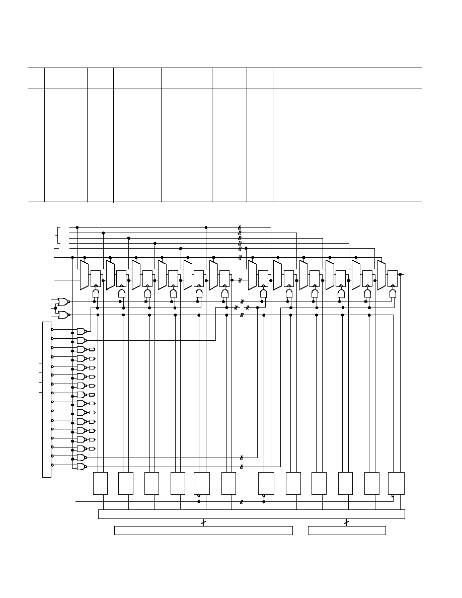
D
CLK
Q
4 TO 16 DECODER
A0
A1
A2
CLK
CE
UPDATE
16
256
DATA IN
(SERIAL)
(OUTPUT
ENABLE)
SER/PAR
RESET
(OUTPUT ENABLE)
OUT0 EN
DATA
OUT
PARALLEL
DATA
D Q
CLK
D Q
CLK
D Q
CLK
D Q
CLK
D1
D2
D3
D Q
CLK
D Q
CLK
D Q
CLK
D Q
CLK
D Q
CLK
OUT1 EN
OUT2 EN
OUT3 EN
OUT4 EN
OUT5 EN
OUT6 EN
OUT7 EN
D
LE
Q
CLR
OUT15
EN
OUTPUT ENABLE
SWITCH MATRIX
S
D1
Q
D0
D0
S
D1
Q
D0
S
D1
Q
D0
S
D1
Q
D0
S
D1
Q
D0
S
D1
Q
D0
S
D1
Q
D0
S
D1
Q
D0
D Q
CLK
S
D1
Q
D0
D4
DECODE
D
LE
Q
CLR
OUT0
EN
D
LE
OUT0
B0
Q
D
LE
Q
OUT0
B1
D
LE
Q
OUT0
B2
D
LE
Q
OUT0
B3
D
LE
OUT1
B0
Q
D
LE
Q
CLR
OUT14
EN
D
LE
OUT15
B0
Q
D
LE
OUT15
B1
Q
D
LE
OUT15
B2
Q
D Q
CLK
S
D1
Q
D0
S
D1
Q
D0
D
LE
OUT15
B3
Q
S
D1
Q
D0
OUT8 EN
OUT9 EN
OUT10 EN
OUT11 EN
OUT12 EN
OUT13 EN
OUT14 EN
OUT15 EN
A3
OUTPUT
ADDRESS
Figure 4. Logic Diagram
REV. A
AD8113
7
PIN FUNCTION DESCRIPTIONS
Mnemonic
Pin Numbers
Pin Description
INxx
58, 60, 62, 64, 66, 68, 70, 72,
Analog Inputs; xx = Channel Numbers 00 through 15.
4, 6, 8, 10, 12, 14, 16, 18
DATA IN
96
Serial Data Input, TTL Compatible.
CLK
97
Clock, TTL Compatible. Falling Edge Triggered.
DATA OUT
98
Serial Data Out, TTL Compatible.
UPDATE
95
Enable (Transparent) Low. Allows serial register to connect directly to switch matrix.
Data latched when High.
RESET
100
Disable Outputs, Active Low.
CE
99
Chip Enable, Enable Low. Must be low to clock in and latch data.
SER/PAR
94
Selects Serial Data Mode, Low or Parallel Data Mode, High. Must be connected.
OUTyy
53, 51, 49, 47, 45, 43, 41, 39,
Analog Outputs yy = Channel Numbers 00 Through 15.
37, 35, 33, 31, 29, 27, 25, 23
AGND
3, 5, 7, 9, 11, 13, 15, 17, 19, 57,
Analog Ground for Inputs and Switch Matrix. Must be connected.
59, 61, 63, 65, 67, 69, 71, 73
DV
CC
1, 75
5 V for Digital Circuitry.
DGND
2, 74
Ground for Digital Circuitry.
AV
EE
20, 56
5 V for Inputs and Switch Matrix.
AV
CC
21, 55
5 V for Inputs and Switch Matrix.
AV
CC
xx/yy
54, 50, 46, 42, 38, 34, 30, 26, 22
5 V for Output Amplifier that is shared by Channel Numbers xx and yy. Must be connected.
AV
EE
xx/yy
52, 48, 44, 40, 36, 32, 28, 24
5 V for Output Amplifier that is shared by Channel Numbers xx and yy. Must be connected.
A0
84
Parallel Data Input, TTL Compatible (Output Select LSB).
A1
83
Parallel Data Input, TTL Compatible (Output Select).
A2
82
Parallel Data Input, TTL Compatible (Output Select).
A3
81
Parallel Data Input, TTL Compatible (Output Select MSB).
D0
80
Parallel Data Input, TTL Compatible (Input Select LSB).
D1
79
Parallel Data Input, TTL Compatible (Input Select).
D2
78
Parallel Data Input, TTL Compatible (Input Select).
D3
77
Parallel Data Input, TTL Compatible (Input Select MSB).
D4
76
Parallel Data Input, TTL Compatible (Output Enable).
NC
8593
No Connect.
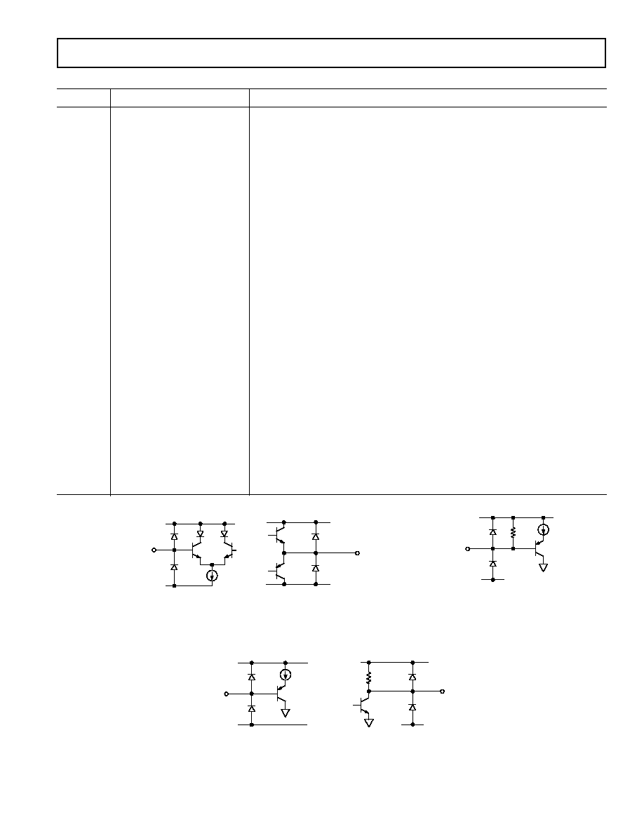
Figure 5. I/O Schematics
ESD
ESD
INPUT
V
CC
AV
EE
a. Analog Input
ESD
ESD
RESET
V
CC
20k
DGND
c. Reset Input
ESD
ESD
OUTPUT
V
CC
AV
EE
b. Analog Output
ESD
ESD
INPUT
V
CC
DGND
d. Logic Input
ESD
ESD
OUTPUT
V
CC
2k
DGND
e. Logic Output

REV. A
AD8113
8
PIN CONFIGURATION
5
4
3
2
7
6
9
8
1
RESET
CE
DATA OUT
CLK
DATA IN
UPDATE
SER
/PAR
NC
NC
NC
NC
NC
NC
NC
NC
NC
A0
A1
A2
A3
AV
CC
13/14
OUT13
AV
EE
12/13
OUT12
AV
CC
11/12
OUT11
AV
EE
10/11
OUT10
AV
CC
09/10
OUT09
AV
EE
08/09
OUT08
AV
CC
07/08
OUT07
AV
EE
06/07
OUT06
AV
CC
05/06
OUT05
AV
EE
04/05
DV
CC
DGND
AGND
IN07
AGND
IN06
AGND
IN05
AGND
IN04
AGND
IN03
AGND
IN02
AGND
IN01
AGND
IN00
AGND
AV
EE
AV
CC
AV
CC
00
OUT00
AV
EE
00/01
OUT01
DV
CC
DGND
AGND
IN08
AGND
IN09
AGND
IN10
AGND
IN11
AGND
IN12
AGND
IN13
AGND
IN14
AGND
IN15
AGND
AV
EE
AV
CC
AV
CC
15
OUT15
AV
EE
14/15
OUT14
D0
D1
D2
D3
D4
OUT04
AV
CC
03/04
OUT03
AV
EE
02/03
OUT02
AV
CC
01/02
71
72
73
74
69
70
67
68
65
66
75
60
61
62
63
58
59
56
57
54
55
64
52
53
51
10
0
99
98
97
96
95
94
93
92
91
90
89
88
87
86
85
84
83
82
81
80
79
78
77
76
PIN 1
IDENTIFIER
TOP VIEW
(Not to Scale)
26
27
28
29
30
31
32
33
34
35
36
37
38
39
40
41
42
43
44
45
46
47
48
49
50
11
10
16
15
14
13
18
17
20
19
22
21
12
24
23
25
AD8113
NC = NO CONNECT
REV. A
AD8113
9
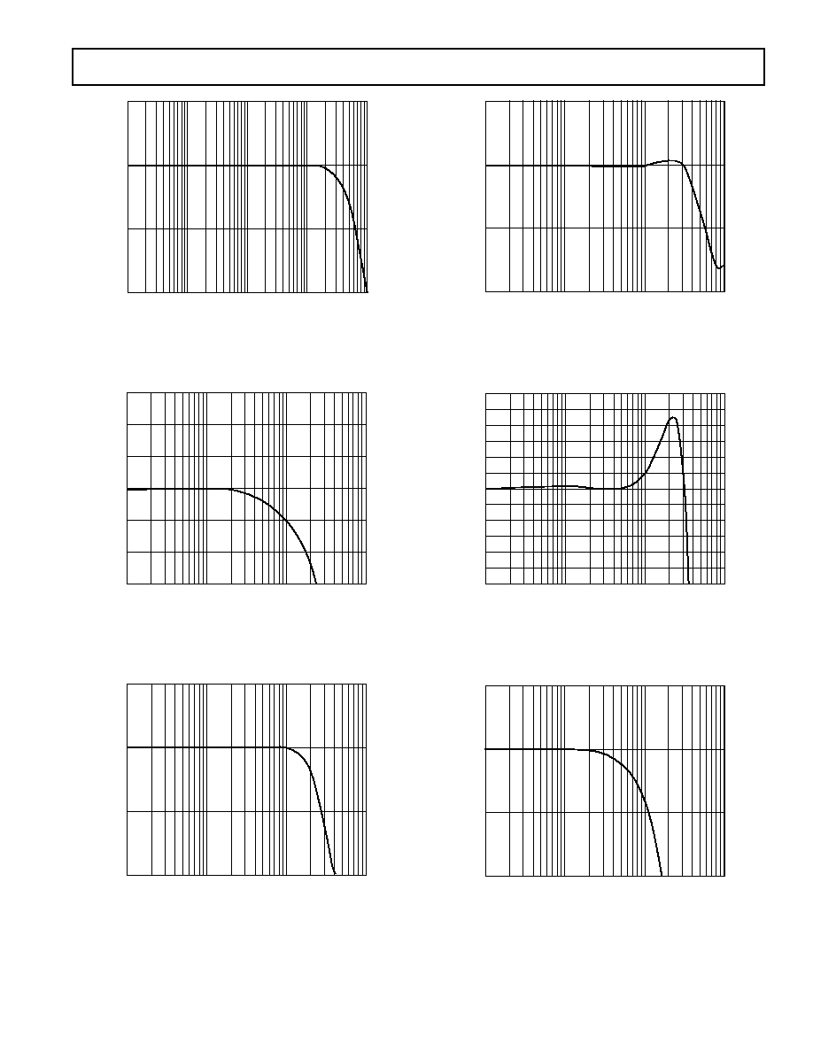
Typical Performance Characteristics
FREQUENCY MHz
GAIN dB
6.0
3.0
0.0
3.0
0.01
100
10
1
0.1
TPC 1. Small Signal Bandwidth, V
S
=
±5 V, R
L
= 150
,
V
OUT
= 200 mV p-p
FREQUENCY MHz
GAIN FLATNESS dB
0.3
0.2
0.1
0.3
0.1
100
10
1
0.0
0.1
0.2
TPC 2. Small Signal Gain Flatness, V
S
=
±5 V, R
L
= 150
,
V
OUT
= 200 mV p-p
FREQUENCY MHz
GAIN dB
6.0
3.0
0.0
3.0
0.1
100
10
1
TPC 3. Large Signal Bandwidth, V
S
=
±5 V, R
L
= 150
,
V
OUT
= 2 V p-p
FREQUENCY MHz
GAIN dB
6.0
3.0
0.0
3.0
0.1
100
10
1
TPC 4. Small Signal Bandwidth, V
S
=
±12 V, R
L
= 600
,
V
OUT
= 200 mV p-p
FREQUENCY MHz
GAIN FLATNESS dB
0.3
0.0
0.2
0.1
0.1
0.2
0.3
0.1
100
10
1
TPC 5. Small Signal Gain Flatness, V
S
=
±12 V, R
L
= 600
,
V
OUT
= 200 mV p-p
FREQUENCY MHz
GAIN dB
6.0
3.0
0.0
3.0
0.1
100
10
1
TPC 6. Large Signal Bandwidth, V
S
=
±12 V, R
L
= 600
,
V
OUT
= 8 V p-p
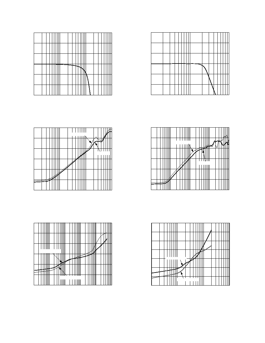
REV. A
AD8113
10
FREQUENCY MHz
GAIN FLATNESS dB
0.3
0.2
0.1
0.3
0.1
100
10
1
0.0
0.1
0.2
TPC 7. Large Signal Gain Flatness, V
S
=
±5 V, R
L
= 150
,
V
OUT
= 2 V p-p
FREQUENCY MHz
CROSSTALK dB
60
40
0.1
100
10
1
ALL HOSTILE
ADJACENT
100
90
80
70
50
TPC 8. Crosstalk vs. Frequency, V
S
=
±5 V, R
L
= 150
,
V
OUT
= 2 V p-p
FREQUENCY MHz
DISTORTION dBc
110
0.001
100
10
0.1
0.01
1
100
90
80
70
60
50
2ND HARMONIC
3RD HARMONIC
TPC 9. Distortion vs. Frequency, V
S
=
±5 V, R
L
= 150
,
V
OUT
= 2 V p-p
GAIN FLATNESS dB
FREQUENCY MHz
0.3
0.0
0.1
10
1
0.2
0.1
0.1
0.2
0.3
TPC 10. Large Signal Gain Flatness, V
S
=
±12 V,
R
L
= 600
, V
OUT
= 8 V p-p
FREQUENCY MHz
CROSSTALK dB
90
0.01
100
10
1
0.1
80
70
60
50
40
30
ALL HOSTILE
ADJACENT
TPC 11. Crosstalk vs. Frequency, V
S
=
±12 V, R
L
= 600
,
V
OUT
= 20 V p-p
DISTORTION dBc
105
100
80
FREQUENCY MHz
0.001
1
0.1
0.01
70
75
85
90
95
3RD HARMONIC
2ND HARMONIC
TPC 12. Distortion vs. Frequency, V
S
=
±12 V, R
L
= 600
,
V
OUT
= 20 V p-p
REV. A
AD8113
11
CAP LOAD pF
SERIES RESISTANCE
0
300
35
250
200
150
100
50
0
5
10
15
20
25
30
V
S
= 12V
R
L
= 600
V
S
= 5V
R
L
= 150
TPC 13. Cap Load vs. Series Resistance for Less than 30%
Overshoot
IMPEDANCE
1
100
1k
10k
10
FREQUENCY MHz
0.1
10
1
100
1000
TPC 14. Disabled Output Impedance vs. Frequency,
V
S
=
±5 V
IMPEDANCE
1
100
1k
10
FREQUENCY MHz
0.1
10
1
100
1000
0.1
TPC 15. Enabled Output Impedance vs. Frequency,
V
S
=
±5 V
INPUT
OUTPUT
5ns/DIV
0
5
10
15
20
25
30
35
40
45
50
0.1%/DIV
OUTPUT
INPUT
2
TPC 16. Settling Time to 0.1%, 2 V Step, V
S
=
±5 V,
R
L
= 150
IMPEDANCE
1
100
1k
10k
10
FREQUENCY MHz
0.1
10
1
100
1000
TPC 17. Disabled Output Impedance vs. Frequency,
V
S
=
±12 V
IMPEDANCE
1
100
1k
10
FREQUENCY MHz
0.1
10
1
100
1000
0.1
TPC 18. Enabled Output Impedance vs. Frequency,
V
S
=
±12 V
REV. A
AD8113
12
FREQUENCY MHz
PSRR dB
90
0.01
10
1
0.1
80
70
60
50
40
30
20
10
0
+PSRR
PSRR
TPC 19. PSRR vs. Frequency, V
S
=
±5 V
NOISE nV/
Hz
FREQUENCY Hz
0
10
100
1k
10k
100k
1M
10M
20
40
60
80
100
120
140
160
TPC 20. Noise vs. Frequency
50ns/DIV
50mV/DIV
TPC 21. Small Signal Pulse Response, V
S
=
±5 V,
R
L
= 150
FREQUENCY MHz
PSRR dB
100
0.01
10
1
0.1
80
60
40
20
0
+PSRR
PSRR
TPC 22. PSRR vs. Frequency, V
S
=
±12 V
FREQUENCY MHz
OFF ISOLATION dB
20
0
0.1
100
10
1
40
60
80
100
120
V
S
= 12V
R
L
= 600
V
OUT
= 8V p-p
V
S
= 5V
R
L
= 150
V
OUT
= 2V p-p
TPC 23. Off Isolation vs. Frequency
100ns/DIV
50mV/DIV
TPC 24. Small Signal Pulse Response, V
S
=
±12 V,
R
L
= 600
REV. A
AD8113
13
100ns/DIV
500mV/DIV
TPC 25. Large Signal Pulse Response, V
S
=
±5 V,
R
L
= 150
100ns/DIV
2V/DIV
TPC 26. Switching Time, V
S
=
±5 V, R
L
= 150
100ns/DIV
1V/DIV
20mV/DIV
OUTPUT
TPC 27. Switching Transient, V
S
=
±5 V, R
L
= 150
100ns/DIV
5V/DIV
TPC 28. Large Signal Pulse Response, V
S
=
±12 V,
R
L
= 600
10V/DIV
100ns/DIV
2V/DIV
TPC 29. Switching Time, V
S
=
±12 V, R
L
= 600
100ns/DIV
1V/DIV
20mV/DIV
OUTPUT
TPC 30. Switching Transient, V
S
=
±12 V, R
L
= 600

REV. A
AD8113
14
THEORY OF OPERATION
The AD8113 is a gain-of-two crosspoint array with 16 outputs,
each of which can be connected to any one of 16 inputs. Organized
by output row, 16 switchable transconductance stages are
connected to each output buffer in the form of a 16-to-1
multiplexer. Each of the 16 rows of transconductance stages
are wired in parallel to the 16 input pins, for a total array of
256 transconductance stages. Decoding logic for each output
selects one (or none) of the transconductance stages to drive the
output stage. The transconductance stages are NPN input
differential pairs, sourcing current into the folded cascode
output stage. The compensation networks and emitter follower
output buffers are in the output stage. Voltage feedback sets the
gain at +2.
When operated with
±12 V supplies, this architecture provides
±10 V drive for 600 audio loads with extremely low distortion
(<0.002%) at audio frequencies. Provided the supplies are lowered
to
±5 V (to limit power consumption), the AD8113 can drive
reverse-terminated video loads, swinging
±3.0 V into 150 .
Disabling unused outputs and transconductance stages minimizes
on-chip power consumption.
Features of the AD8113 facilitate the construction of larger
switch matrices. The unused outputs can be disabled, leaving
only a feedback network resistance of 4 k
on the output. This
allows multiple ICs to be bused together, provided the output
load impedance is greater than minimum allowed values. Because
no additional input buffering is necessary, high input resistance
and low input capacitance are easily achieved without additional
signal degradation.
The AD8113 inputs have a unique bias current compensation
scheme that overcomes a problem common to transconductance
input array architectures. Typically, input bias current increases
as more and more transconductance stages connected to the same
input are turned on. Anywhere from zero to 16 transconductance
stages can be sharing one input pin, so there is a varying amount
of bias current supplied through the source impedance driving
the input. For audio systems with larger source impedances,
this has the potential of creating large offset voltages, audible
as pops when switching between channels. The AD8113 samples
and cancels the input bias current contributions from each
transconductance stage so that the residual bias current is nomi-
nally zero regardless of the number of enabled inputs.
Due to the flexibility in allowed supply voltages, internal crosstalk
isolation clamps have variable bias levels. These levels were
chosen to allow for the necessary input range to accommodate
the full output swing with a gain of two. Overdriving the inputs
beyond the device's linear range will eventually forward bias
these clamps, increasing power dissipation. The valid input
range for
± 12 V supplies is ± 5 V. The valid input range for
±5 V supplies is ±1.5 V. When outputs are disabled and being
driven externally, the voltage applied to them should not exceed
the valid output swing range for the AD8113. Exceeding
±10.5 V
on the outputs of the AD8113 may apply a large differential voltage
on the unused transconductance stages and should be avoided.
A flexible TTL compatible logic interface simplifies the program-
ming of the matrix. Either parallel or serial loading into a first
rank of latches programs each output. A global latch simulta-
neously updates all outputs. In serial mode, a serial-out pin allows
devices to be daisy chained together for single pin programming
of multiple ICs. A power-on reset pin is available to avoid bus
conflicts by disabling all outputs.
Regardless of the supply voltage applied to the AV
CC
and AV
EE
pins, the digital logic requires 5 V on the DV
CC
pin with respect
to DGND. In order for the digital-to-analog interface to work
properly, DV
CC
must be at least 7 V above AV
EE
. Finally, internal
ESD protection diodes require that the DGND and AGND pins
be at the same potential.
REV. A
AD8113
15
CALCULATION OF POWER DISSIPATION
AMBIENT TEMPERATURE C
0
70
2.0
3.0
4.0
3.5
2.5
60
50
40
30
20
10
MAXIMUM POWER Watts
T
J
= 150 C
Figure 6. Maximum Power Dissipation vs. Ambient
Temperature
The above curve was calculated from
P
T
T
D MAX
NCTION MAX
AMBIENT
A
,
,
=
(
)
JU
J
As an example, if the AD8113 is enclosed in an environment at
50
°C (T
A
), the total on-chip dissipation under all load and supply
conditions must not be allowed to exceed 2.5 W.
When calculating on-chip power dissipation, it is necessary to
include the rms current being delivered to the load, multiplied
by the rms voltage drop on the AD8113 output devices. The
dissipation of the on-chip, 4 k
feedback resistor network must
also be included. For a sinusoidal output, the on-chip power
dissipation due to the load and feedback network can be approxi-
mated by
P
AV
V
I
V
k
D MAX
CC
OUTPUT RMS
OUTPUT RMS
OUTPUT RMS
,
,
,
,
=
(
)
×
+
2
4
For nonsinusoidal output, the power dissipation should be cal-
culated by integrating the on-chip voltage drop multiplied by the
load current over one period.
The user may subtract the quiescent current for the Class AB
output stage when calculating the loaded power dissipation. For
each output stage driving a load, subtract a quiescent power
according to
P
AV
AV
I
D OUTPUT
CC
EE
O QUIESCENT
,
,
=
(
)
×
For the AD8113, I
O, QUIESCENT
= 0.67 mA.
For each disabled output, the quiescent power supply current in
AV
CC
and AV
EE
drops by approximately 1.25 mA, although
there is a power dissipation in the on-chip feedback resistors if
the disabled output is being driven from an external source.
AGND
RF
4k
AV
EE
I
O, QUIESCENT
QPNP
V
OUTPUT
I
OUTPUT
QNPN
AV
CC
I
O, QUIESCENT
Figure 7. Simplified Output Stage
An example: AD8113, in an ambient temperature of 70
°C,
with all 16 outputs driving 6 V rms into 600
loads. Power
supplies are
±12 V.
Step 1. Calculate power dissipation of AD8113 using data sheet
quiescent currents.
P
D, QUIESCENT
= (AV
CC
× I
AVCC
) + (AV
EE
× I
AVEE
) + (DV
CC
× I
DVCC
)
P
D, QUIESCENT
= (12 V
× 54 mA) + (12 V × 54 mA)
+ (5 V
× 13 mA)
Step 2. Calculate power dissipation from loads.
P
D, OUTPUT
= (AV
CC
V
OUTPUT, RMS
)
× I
OUTPUT, RMS
+ V
OUTPUT
2
/4 k
P
D, OUTPUT
= (12 V 6 V)
× 6 V/600 + (6 V)
2
/4 k
= 69 mW
There are 16 outputs, so
nP
D, OUTPUT
= 16
× 69 mW = 1.1 W
Step 3. Subtract quiescent output current for number of loads
(assumes output voltage >> 0.5 V).
P
DQ, OUTPUT
= (AV
CC
AV
EE
)
× I
O, QUIESCENT
P
DQ, OUTPUT
= (12 V (12 V))
× 0.67 mA = 16 mW
There are 16 outputs, so
nP
D, OUTPUT
= 16
× 16 mW = 0.3 W
Step 4. Verify that power dissipation does not exceed maximum
allowed value.
P
D, ON-CHIP
= P
D, QUIESCENT
+ nP
D, OUTPUT
nP
DQ, OUTPUT
P
D, ON-CHIP
= 1.3 W + 1.1 W 0.3 W = 2.1 W
From the figure or the equation, this power dissipation is below
the maximum allowed dissipation for all ambient temperatures
approaching 70
°C.
NOTE: It can be shown that for a dual supply of
±a, a Class AB
output stage dissipates maximum power into a grounded load
when the output voltage is a/2. So for a
± 12 V supply, the
above example demonstrates the worst-case power dissipation
into 600
. It can be seen from this example that the minimum
load resistance for
±12 V operation is 600 (for full rated oper-
ating temperature range). For larger safety margins, when the out-
put signal is unknown, loads of 1 k
and greater are recommended.
When operating with
±5 V supplies, this load resistance may be
lowered to 150
.

REV. A
AD8113
16
SHORT-CIRCUIT OUTPUT CONDITIONS
Although there is short-circuit current protection on the AD8113
outputs, the output current can reach values of 55 mA into a
grounded output. Any sustained operation with even one shorted
output will exceed the maximum die temperature and can result
in device failure (see Absolute Maximum Ratings).
APPLICATIONS
The AD8113 has two options for changing the programming of
the crosspoint matrix. In the first option a serial word of 80 bits
can be provided that will update the entire matrix each time.
The second option allows for changing a single output's pro-
gramming via a parallel interface. The serial option requires
fewer signals, but more time (clock cycles) for changing the
programming, while the parallel programming technique requires
more signals, but can change a single output at a time and requires
fewer clock cycles to complete programming.
Serial Programming
The serial programming mode uses the device pins
CE, CLK,
DATA IN,
UPDATE, and SER/PAR. The first step is to assert a
LOW on
SER/PAR in order to enable the serial programming
mode.
CE for the chip must be LOW to allow data to be clocked
into the device. The
CE signal can be used to address an indi-
vidual device when devices are connected in parallel.
The
UPDATE signal should be high during the time that data is
shifted into the device's serial port. Although the data will still
shift in when
UPDATE is LOW, the transparent, asynchronous
latches will allow the shifting data to reach the matrix. This will
cause the matrix to try to update to every intermediate state as
defined by the shifting data.
The data at DATA IN is clocked in at every down edge of CLK.
A total of 80 bits must be shifted in to complete the program-
ming. For each of the 16 outputs, there are four bits (D0D3)
that determine the source of its input followed by one bit (D4)
that determines the enabled state of the output. If D4 is LOW
(output disabled), the four associated bits (D0D3) do not mat-
ter, because no input will be switched to that output.
The most-significant-output-address data is shifted in first, then
following in sequence until the least-significant-output-address
data is shifted in. At this point
UPDATE can be taken low, which
will cause the programming of the device according to the data that
was just shifted in. The
UPDATE registers are asynchronous and
when
UPDATE is low (and CE is low), they are transparent.
If more than one AD8113 device is to be serially programmed in a
system, the DATA OUT signal from one device can be connected
to the DATA IN of the next device to form a serial chain. All of
the CLK,
CE, UPDATE, and SER/PAR pins should be connected
in parallel and operated as described above. The serial data is input
to the DATA IN pin of the first device of the chain, and it will
ripple through to the last. Therefore, the data for the last device
in the chain should come at the beginning of the programming
sequence. The length of the programming sequence will be 80 bits
times the number of devices in the chain.
Parallel Programming
When using the parallel programming mode, it is not necessary to
reprogram the entire device when making changes to the matrix.
In fact, parallel programming allows the modification of a single
output at a time. Since this takes only one CLK/
UPDATE
cycle, significant time savings can be realized by using parallel
programming.
One important consideration in using parallel programming is
that the
RESET signal DOES NOT RESET ALL REGISTERS
in the AD8113. When taken LOW, the
RESET signal will only
set each output to the disabled state. This is helpful during
power-up to ensure that two parallel outputs will not be active
at the same time.
After initial power-up, the internal registers in the device will
generally have random data, even though the
RESET signal has
been asserted. If parallel programming is used to program one
output, then that output will be properly programmed, but the
rest of the device will have a random program state depending
on the internal register content at power-up. Therefore, when
using parallel programming, it is essential that ALL OUTPUTS
BE PROGRAMMED TO A DESIRED STATE AFTER
POWER-UP. This will ensure that the programming matrix is
always in a known state. From then on, parallel programming
can be used to modify a single output or more at a time.
In similar fashion, if both
CE and UPDATE are taken LOW
after initial power-up, the random power-up data in the shift
register will be programmed into the matrix. Therefore, in order
to prevent the crosspoint from being programmed into an un-
known state, DO NOT APPLY LOW LOGIC LEVELS TO
BOTH
CE AND UPDATE AFTER POWER IS INITIALLY
APPLIED. Programming the full shift register one time to a
desired state, by either serial or parallel programming after
initial power-up, will eliminate the possibility of programming
the matrix to an unknown state.
To change an output's programming via parallel programming,
SER/PAR and UPDATE should be taken HIGH and CE should
be taken LOW. The CLK signal should be in the HIGH state.
The 4-bit address of the output to be programmed should be put
on A0A3. The first four data bits (D0D3) should contain the
information that identifies the input that gets programmed to the
output that is addressed. The fifth data bit (D4) will determine
the enabled state of the output. If D4 is LOW (output disabled),
then the data on D0D3 does not matter.
After the desired address and data signals have been established,
they can be latched into the shift register by a high to low
transition of the CLK signal. The matrix will not be programmed,
however, until the
UPDATE signal is taken low. It is thus pos-
sible to latch in new data for several or all of the outputs first via
successive negative transitions of CLK while
UPDATE is held
HIGH, and then have all the new data take effect when
UP-
DATE goes LOW. This is the technique that should be used
when programming the device for the first time after power-up
when using parallel programming.
POWER-ON RESET
When powering up the AD8113, it is usually desirable to have
the outputs come up in the disabled state. The
RESET pin,
when taken LOW, will cause all outputs to be in the disabled
state. However, the
RESET signal DOES NOT RESET ALL
REGISTERS in the AD8113. This is important when operating
in the parallel programming mode. Please refer to that section
for information about programming internal registers after
power-up. Serial programming will program the entire matrix
each time, so no special considerations apply.
REV. A
AD8113
17
Since the data in the shift register is random after power-up, it
should not be used to program the matrix, or the matrix can enter
unknown states. To prevent this, DO NOT APPLY LOGIC
LOW SIGNALS TO BOTH
CE AND UPDATE INITIALLY
AFTER POWER-UP. The shift register should first be loaded
with the desired data, and then
UPDATE can be taken LOW to
program the device.
The
RESET pin has a 20 k
pull-up resistor to DV
CC
that can
be used to create a simple power-up reset circuit. A capacitor
from
RESET to ground will hold RESET low for some time
while the rest of the device stabilizes. The low condition will
cause all the outputs to be disabled. The capacitor will then
charge through the pull-up resistor to the high state, thus allow-
ing full programming capability of the device.
SPECIFYING AUDIO LEVELS
Several methods are used to specify audio levels. A level is
actually a power measurement, which requires not just a voltage
measurement, but also a reference impedance. Traditionally
both 150
and 600 have been used as references for audio
level measurements.
The typical reference power level is one milliwatt. Power levels
that are measured relative to this reference level are given the
designation dBm. However, it is always necessary to be sure of
the reference impedance used for such measurements. This can
be either explicit, e.g., 0 dBm (600
), or implicit, if there is
certain agreement on what the reference impedance is.
Since modern voltmeters have high input impedances, measure-
ments can be made that do not terminate the signal. Therefore,
it is not proper to consider this type of measurement a dBm, or
power measurement. However, a measurement scale that is
designated dBu is now used to measure unterminated voltages.
This scale has a voltage reference for 0 dBu that is the same as
the voltage required to produce 0 dBm (600
).
Since P = V
2
/R, the voltage required to create 1 mW into 600
is 0.775 V rms. This is the voltage reference (0 dB) used for
dBu measurements without regard to the impedance.
The AD8113 operates as a voltage-in, voltage-out device.
Therefore, it is easiest to specify all of its parameters in volts,
and leave it to the user to convert them to other power units or
dB-type measurements as required by the particular application.
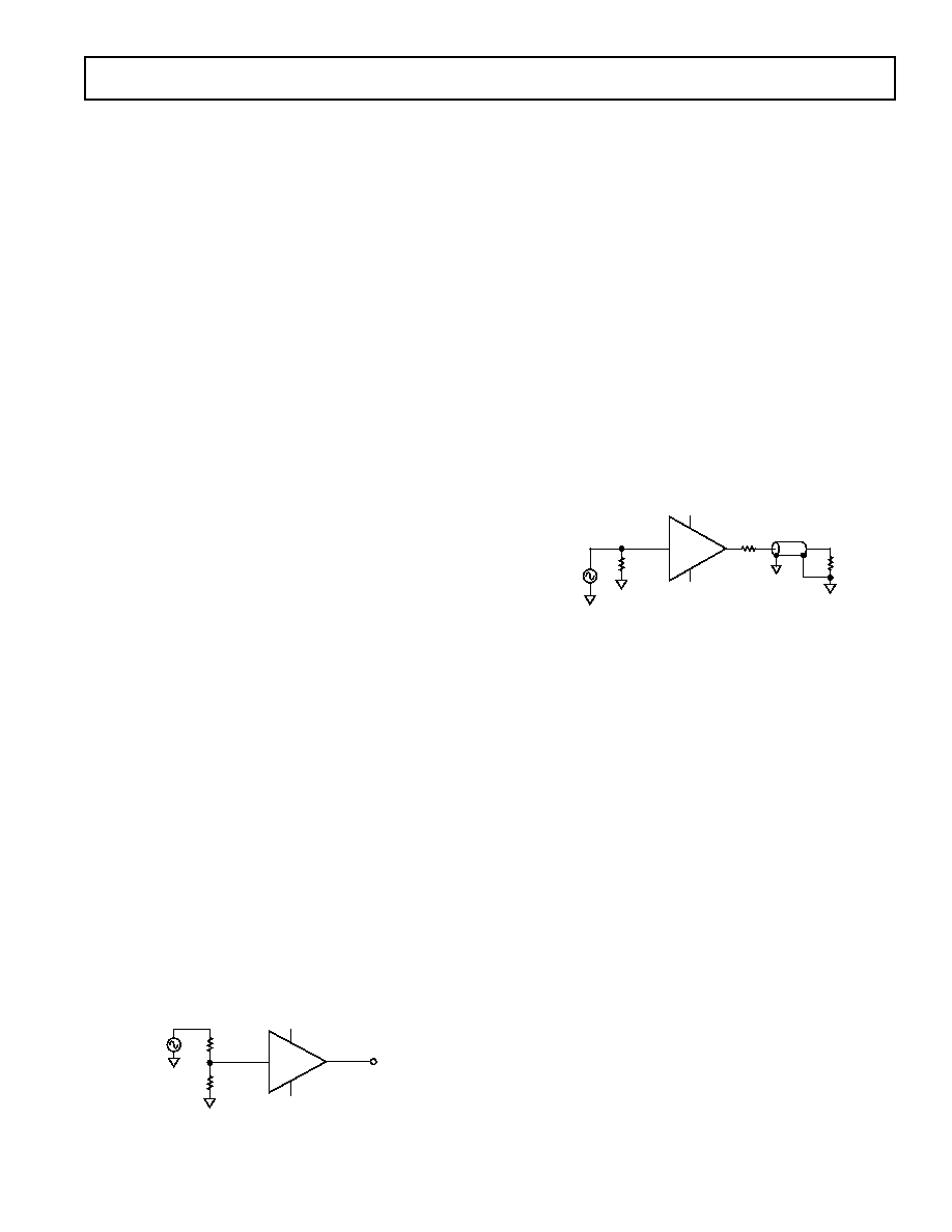
CREATING UNITY-GAIN CHANNELS
The channels in the AD8113 have a gain of two. This gain is
necessary as opposed to a gain of unity in order to restrict the
voltage on internal nodes to less than the breakdown voltage. If
it is desired to create channels with an overall gain of unity,
then a resistive divider at the input will divide the signals by
two. After passing through any input/output channel combina-
tion of the AD8113, the overall gain will be unity.
TYPICAL
INPUT
1k
1k
AD8113
G = 2
+12V
12V
TYPICAL
OUTPUT
UNITY GAIN
AUDIO OUT
AUDIO
SOURCE
Figure 8. Input Divide Circuit
Figure 8 shows a typical input with a divide-by-two input
divider that will create a unity gain channel. The circuit uses 1 k
resistors to form the divider. These resistors need to be high
enough so they will not overload the drive circuit. But if they are
too high, they will generate an offset voltage due to the input bias
current that flows through them. Larger resistors will also increase
the thermal noise of the channel.
This circuit can handle inputs that swing up to
±10 V when
the AD8113 operates on analog supplies of
±12 V. After the
divider, the maximum voltage will be
±5 V at the input. This
maximum input amplitude will be
±10 V at the output after the
gain-of-two of the channel.
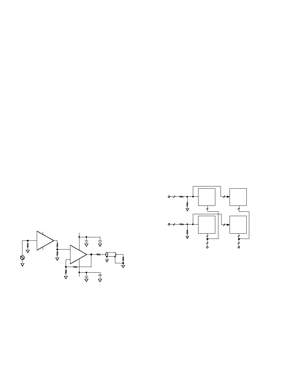
VIDEO SIGNALS
Unlike audio signals, which have lower bandwidths and longer
wavelengths, video signals often use controlled-impedance
transmission lines that are terminated in their characteristic
impedance. While this is not always the case, there are some
considerations when using the AD8113 to route video signals with
controlled-impedance transmission lines. Figure 9 shows a sche-
matic of an input and output treatment of a typical video channel.
75
VIDEO
SOURCE
75
AD8113
G = 2
+5V
OR +12V
TYPICAL
INPUT
5V
OR 12V
TYPICAL
OUTPUT
75
75
TRANSMISSION
LINE
75
Figure 9. Video Signal Circuit
Video signals usually use 75
transmission lines that need to be
terminated with this value of resistance at each end. When such
a source is delivered to one of the AD8113 inputs, the high
input impedance will not properly terminate these signals. There-
fore, the line should be terminated with a 75
shunt resistor to
ground. Since video signals are limited in their peak-to-peak
amplitude, there is no need to attenuate video signals before
they pass through the AD8113.
The AD8113 outputs are very low impedance and will not prop-
erly terminate the source end of a 75
transmission line. In these
cases, a series 75
resistor should be inserted at an output that
will drive a video signal. Then the transmission line should be
terminated with 75
at its far end. This overall termination
scheme will divide the amplitude of the AD8113 output by two.
An overall unity gain channel is produced as a result of the
channel gain-of-two of the AD8113.
Power Considerations of Video Signals
If the AD8113 is used only to route conventional video signals,
runing on analog supplies of
±5 V is recommended. This is all
that is necessary for video signals because they are limited in
their amplitude to generally less than 2 V p-p at the output,
after the channel gain-of-two. There will be significant power
savings when routing video signals with lower supply voltages.
If an AD8113 is used to route a mix of audio and video signals,
then other factors must be considered. In general, the analog
supplies will be at
±12 V to handle the high signal levels required
for the audio.
REV. A
AD8113
18
Inputs and outputs should be preassigned to be either audio or
video. As described above, audio and video signals are treated
differently, so it is difficult to have the same AD8113 inputs or
outputs route audio or video signals in the same system at
different times. The various audio and video channels should
be configured as described in the above sections.
Video outputs that drive a terminated 75
transmission line
(150
equivalent load) will dissipate significantly more power
with
±12 V supplies. An upper bound on power dissipation can
be approximated by the following method.
A video signal at the AD8113 output can have a maximum
value of 2 V. This is quite conservative, because most video
signals are about 700 mV peak at unity gain or 1.4 V peak after
a gain-of-two. A video signal only reaches this level when the video
content is at peak white, so this value is even more pessimistic.
Finally, a video signal will generally have some kind of sync and
blanking interval where its amplitude will be either 0 V (or black)
or very close to this level. The power dissipation will be much
lower during this period and this will occur at a very regular
duty cycle.
If the full 2 V signal is assumed to be present at 100% duty
cycle at the output, then the current in the output is 2 V/150
= 13.3 mA. If the positive supply is at 12 V, there will be a
10 V drop in the AD8113 output stage from the supply to the
output. This yields a power dissipated in the output of 133 mW
from one video load when running on supplies of
±12 V. This
is by far a worst-case situation, and this power dissipation fac-
tor can be adjusted lower by adjusting for actual video levels,
sync-interval duty cycle, and average picture level considerations.
If too much power will be dissipated in this type of configuration,
it is possible to lower it by buffering the output. An AD8113
video output drives a divide-by-two resistive divider that is
made up of two 1 k
resistors. This presents a total load of
2 k
to the AD8113 outputs, which significantly reduces the
power dissipation. Refer to Figure 10.
AD8057
3
2
1k
1k
7
4
6
+5V
5V
0.1 F
10 F
75
75
TRANSMISSION
LINE
75
75
TYPICAL
INPUT
AD8113
G = 2
+12V
12V
1k
1k
0.1 F
10 F
TYPICAL
OUTPUT
+
+
+
Figure 10. Video Buffer Circuit
After this divider, the signal is now at a unity level because of
the channel gain of the AD8113 and the attenuation of the
divider. An AD8057 is configured as a gain-of-two buffer to
drive the terminated transmission line. The AD8058 is a dual
version of the AD8057.
The maximum supply voltage of the AD8057 is only about
±6 V. If the only system supplies that are available are ±12 V, a
higher voltage video op amp can be substituted for the AD8057.
Good candidates are the AD817 and AD818 or, if dual op amps
are needed, the AD826 and AD828.
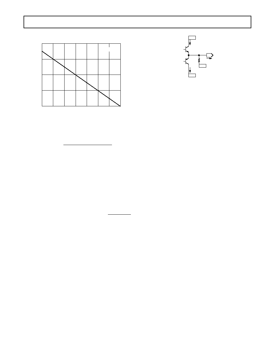
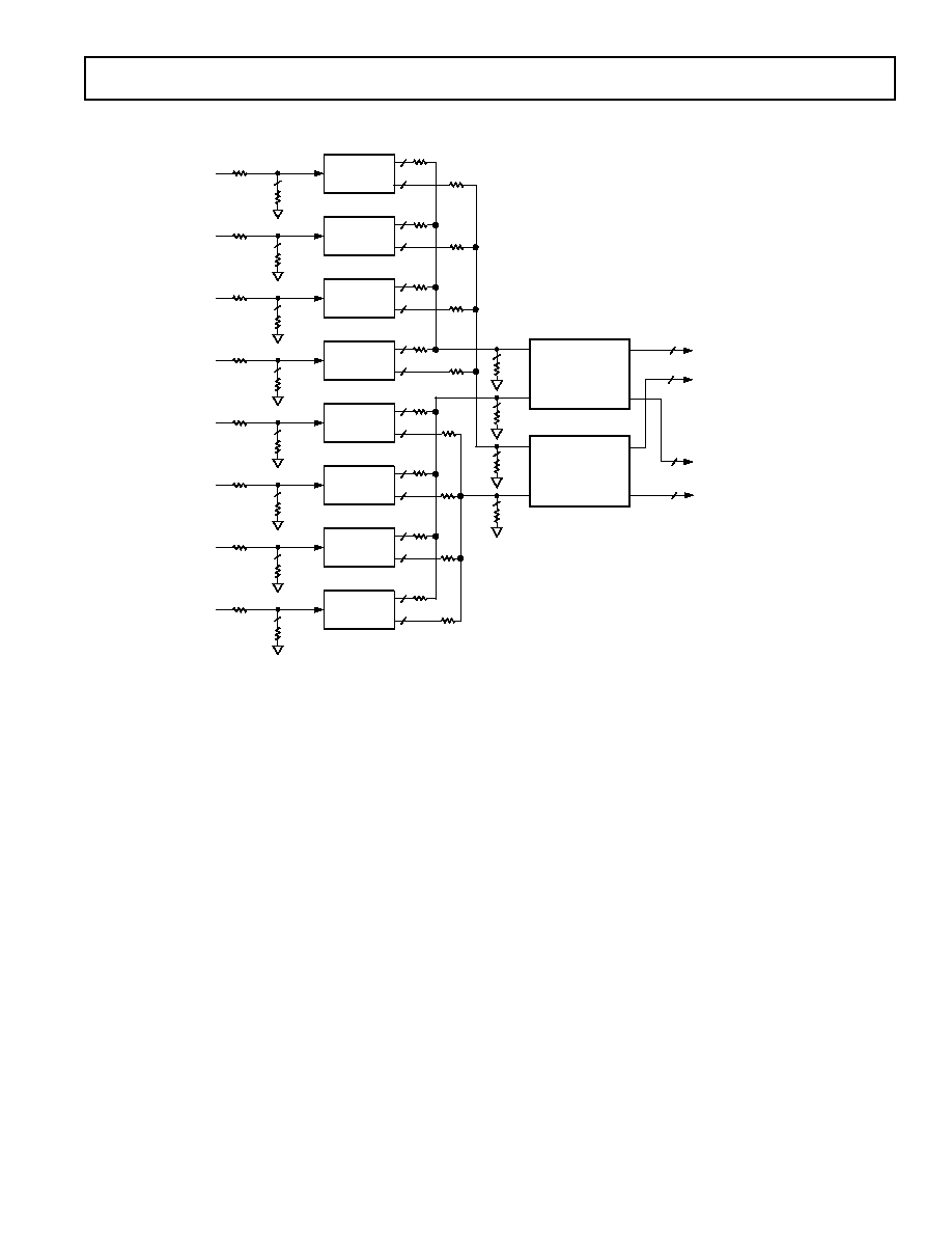
CREATING LARGER CROSSPOINT ARRAYS
The AD8113 is a high density building block for creating cross-
point arrays of dimensions larger than 16
× 16. Various features,
such as output disable and chip enable, are useful for creating
larger arrays.
The first consideration in constructing a larger crosspoint is to
determine the minimum number of devices required. The 16
× 16
architecture of the AD8113 contains 256 points, which is a
factor of 64 greater than a 4
× 1 crosspoint (or multiplexer). The
PC board area, power consumption, and design effort savings are
readily apparent when compared to using these smaller devices.
For a nonblocking crosspoint, the number of points required is
the product of the number of inputs multiplied by the number
of outputs. Nonblocking requires that the programming of a given
input to one or more outputs does not restrict the availability of
that input to be a source for any other outputs.
Some nonblocking crosspoint architectures will require more than
this minimum as calculated above. Also, there are blocking archi-
tectures that can be constructed with fewer devices than this
minimum. These systems have connectivity available on a statis-
tical basis that is determined when designing the overall system.
The basic concept in constructing larger crosspoint arrays is
to connect inputs in parallel in a horizontal direction and to
wire-OR the outputs together in the vertical direction. The
meaning of horizontal and vertical can best be understood by
looking at a diagram. Figure 11 illustrates this concept for a
32
× 32 crosspoint array that uses four AD8113s.
1k
AD8113
AD8113
IN 00 15
IN 16 31
AD8113
AD8113
1k
1k
1k
16
16
16
16
16
16
16
16
16
16
Figure 11. 32
× 32 Audio Crosspoint Array Using Four
AD8113s
The inputs are individually assigned to each of the 32 inputs of
the two devices and a divider is used to normalize the channel
gain. The outputs are wire-ORed together in pairs. The output
from only one of a wire-ORed pair should be enabled at any
given time. The device programming software must be properly
written to cause this to happen.
Using additional crosspoint devices in the design can lower the
number of outputs that have to be wire-ORed together. Figure 12
shows a block diagram of a system using ten AD8113s to create
a nonblocking, gain-of-two, 128
× 16 crosspoint that restricts
the wire-ORing at the output to only four outputs.
Additionally, by using the lower eight outputs from each of the
two Rank 2 AD8113s, a blocking 128
× 32 crosspoint array can be
realized. There are, however, some drawbacks to this technique.
The offset voltages of the various cascaded devices will accumu-
REV. A
AD8113
19
late, and the bandwidth limitations of the devices will com-
pound. In addition, the extra devices will consume more current
and take up more board space. Once again, the overall system
design specifications will determine how to make the various
trade-offs.
Multichannel Video and Audio
The good video specifications of the AD8113 make it an ideal
candidate for creating composite video crosspoint switches. These
can be made quite dense by taking advantage of the AD8113's
high level of integration and the fact that composite video requires
only one crosspoint channel per system video channel. There are,
however, other video formats that can be routed with the AD8113,
requiring more than one crosspoint channel per video channel.
Some systems use twisted-pair wiring to carry video or audio sig-
nals. These systems utilize differential signals and can lower costs
because they use lower cost cables, connectors, and termination
methods. They also have the ability to lower crosstalk and reject
common-mode signals, which can be important for equipment that
operates in noisy environments, or where common-mode voltages
are present between transmitting and receiving equipment.
In such systems, the audio or video signals are differential; there
are positive and negative (or inverted) versions of the signals.
These complementary signals are transmitted onto each of the
two wires of the twisted pair, yielding a first order zero common-
mode voltage. At the receive end, the signals are differentially
received and converted back into a single-ended signal.
When switching these differential signals, two channels are
required in the switching element to handle the two differential
signals that make up the video or audio channel. Thus, one
differential video or audio channel is assigned to a pair of
crosspoint channels, both input and output. For a single AD8113,
eight differential video or audio channels can be assigned to the
16 inputs and 16 outputs. This will effectively form an 8
× 8
differential crosspoint switch.
Programming such a device will require that inputs and outputs be
programmed in pairs. This information can be deduced through
inspection of the programming format of the AD8113 and the
requirements of the system.
There are other analog video formats requiring more than one
analog circuit per video channel. One two-circuit format that is
commonly being used in systems such as satellite TV, digital
cable boxes, and higher quality VCRs, is called S-video or Y/C
video. This format carries the brightness (luminance or Y)
portion of the video signal on one channel and the color (chromi-
nance, chroma, or C) on a second channel.
Since S-video also uses two separate circuits for one video channel,
creating a crosspoint system requires assigning one video channel
to two crosspoint channels as in the case of a differential video
system. Aside from the nature of the video format, other aspects
of these two systems will be the same. Stereo audio can also be
routed in a paired-channel arrangement similar to a two-channel
video system.
16
R
TERM
IN 0015
8
8
IN 1631
IN 3247
IN 4863
IN 64 79
IN 8095
IN 96 111
IN 112 127
8
8
8
8
RANK 2
32:16 NONBLOCKING
(32:32 BLOCKING)
RANK 1
(8 AD8113)
128:32
R
TERM
8
8
R
TERM
8
8
R
TERM
8
8
R
TERM
8
8
R
TERM
8
8
R
TERM
8
8
R
TERM
8
8
8
1k
8
1k
8
1k
8
1k
AD8113
OUT 00 15
NONBLOCKING
ADDITIONAL
16 OUTPUTS
(SUBJECT
TO BLOCKING)
AD8113
AD8113
AD8113
AD8113
AD8113
AD8113
AD8113
AD8113
1k
1k
1k
1k
1k
1k
1k
1k
16
16
16
16
16
16
16
1k
1k
1k
1k
1k
1k
1k
1k
1k
1k
1k
1k
1k
1k
1k
1k
AD8113
Figure 12. Nonblocking 128
× 16 Audio Array (128 × 32 Blocking)

REV. A
AD8113
20
There are yet other video formats using three channels to carry
the video information. Video cameras produce RGB (red, green,
blue) directly from the image sensors. RGB is also the usual
format used by computers internally for graphics. RGB can also
be converted to Y, RY, BY format, sometimes called YUV
format. These three-circuit video standards are referred to as
component analog video.
The component video standards require three crosspoint chan-
nels per video channel to handle the switching function. In a
fashion similar to the two-circuit video formats, the inputs and
outputs are assigned in groups of three and the appropriate logic
programming is performed to route the video signals.
CROSSTALK
Many systems, such as studio audio or broadcast video, that
handle numerous analog signal channels, have strict requirements
for keeping the various signals from influencing any of the others in
the system. Crosstalk is the term used to describe the coupling
of the signals of other nearby channels to a given channel.
When there are many signals in close proximity in a system, as
will undoubtedly be the case in a system that uses the AD8113,
the crosstalk issues can be quite complex. A good understanding
of the nature of crosstalk and some definition of terms is required
in order to specify a system that uses one or more AD8113s.
Types of Crosstalk
Crosstalk can be propagated by means of any of three methods.
These fall into the categories of electric field, magnetic field,
and sharing of common impedances. This section will explain
these effects.
Every conductor can be both a radiator of electric fields and a
receiver of electric fields. The electric field crosstalk mechanism
occurs when the electric field created by the transmitter propa-
gates across a stray capacitance (e.g., free space) and couples with
the receiver and induces a voltage. This voltage is an unwanted
crosstalk signal in any channel that receives it.
Currents flowing in conductors create magnetic fields that circulate
around the currents. These magnetic fields then generate voltages
in any other conductors whose paths they link. The undesired
induced voltages in these other channels are crosstalk signals. The
channels that crosstalk can be said to have a mutual inductance
that couples signals from one channel to another.
The power supplies, grounds, and other signal return paths of a
multichannel system are generally shared by the various chan-
nels. When a current from one channel flows in one of these
paths, a voltage that is developed across the impedance becomes
an input crosstalk signal for other channels that share the com-
mon impedance.
All these sources of crosstalk are vector quantities, so the mag-
nitudes cannot simply be added together to obtain the total
crosstalk. In fact, there are conditions where driving additional
circuits in parallel in a given configuration can actually reduce
the crosstalk.
Areas of Crosstalk
A practical AD8113 circuit must be mounted to some sort of
circuit board in order to connect it to power supplies and
measurement equipment. Great care has been taken to create a
characterization board (also available as an evaluation board) that
adds minimum crosstalk to the intrinsic device. This, however,
raises the issue that a system's crosstalk is a combination of the
intrinsic crosstalk of the devices in addition to the circuit board
to which they are mounted. It is important to try to separate these
two areas when attempting to minimize the effect of crosstalk.
In addition, crosstalk can occur among the inputs to a cross-
point and among the outputs. It can also occur from input to
output. Techniques will be discussed for diagnosing which part
of a system is contributing to crosstalk.
Measuring Crosstalk
Crosstalk is measured by applying a signal to one or more chan-
nels and measuring the relative strength of that signal on a desired
selected channel. The measurement is usually expressed as dB
down from the magnitude of the test signal. The crosstalk is
expressed by
XT
Asel s
Atest s
=
( )
( )
(
)
20
10
log
where s = jw is the Laplace transform variable, Asel(s) is the
amplitude of the crosstalk induced signal in the selected channel,
and Atest(s) is the amplitude of the test signal. It can be seen
that crosstalk is a function of frequency, but not a function of
the magnitude of the test signal (to first order). In addition,
the crosstalk signal will have a phase relative to the test signal
associated with it.
A network analyzer is most commonly used to measure crosstalk
over a frequency range of interest. It can provide both magnitude
and phase information about the crosstalk signal.
As a crosspoint system or device grows larger, the number of
theoretical crosstalk combinations and permutations can become
extremely large. For example, in the case of the 16
× 16 matrix
of the AD8113, look at the number of crosstalk terms that can
be considered for a single channel, say the IN00 input. IN00
is programmed to connect to one of the AD8113 outputs where
the measurement can be made.
First, the crosstalk terms associated with driving a test signal into
each of the other 15 inputs can be measured one at a time, while
applying no signal to IN00. Then the crosstalk terms associated
with driving a parallel test signal into all 15 other inputs can be
measured two at a time in all possible combinations, then three
at a time, and so on, until, finally, there is only one way to drive
a test signal into all 15 other inputs in parallel.
Each of these cases is legitimately different from the others and
might yield a unique value, depending on the resolution of the
measurement system, but it is hardly practical to measure all
these terms and then specify them. In addition, this describes
the crosstalk matrix for just one input channel. A similar cross-
talk matrix can be proposed for every other input. In addition, if
the possible combinations and permutations for connecting
inputs to the other outputs (not used for measurement) are
taken into consideration, the numbers rather quickly grow to
astronomical proportions. If a larger crosspoint array of multiple
AD8113s is constructed, the numbers grow larger still.
Obviously, some subset of all these cases must be selected to
be used as a guide for a practical measure of crosstalk. One
common method is to measure all hostile crosstalk; this means
that the crosstalk to the selected channel is measured while all
other system channels are driven in parallel. In general, this will
yield the worst crosstalk number, but this is not always the case,
due to the vector nature of the crosstalk signal.

REV. A
AD8113
21
Other useful crosstalk measurements are those created by one
nearest neighbor or by the two nearest neighbors on either side.
These crosstalk measurements will generally be higher than those
of more distant channels, so they can serve as a worst-case measure
for any other one-channel or two-channel crosstalk measurements.
Input and Output Crosstalk
The flexible programming capability of the AD8113 can be
used to diagnose whether crosstalk is occurring more on the
input side or the output side. Some examples are illustrative. A
given input channel (IN07 in the middle for this example)
can be programmed to drive OUT07 (also in the middle). The
input to IN07 is just terminated to ground (via 50
or 75 )
and no signal is applied.
All the other inputs are driven in parallel with the same test
signal (practically provided by a distribution amplifier), with all
other outputs except OUT07 disabled. Since grounded IN07 is
programmed to drive OUT07, no signal should be present. Any
signal that is present can be attributed to the other 15 hostile input
signals, because no other outputs are driven (they are all disabled).
Thus, this method measures the all-hostile input contribution to
crosstalk into IN07. Of course, the method can be used for other
input channels and combinations of hostile inputs.
For output crosstalk measurement, a single input channel is
driven (IN00, for example) and all outputs other than a given
output (IN07 in the middle) are programmed to connect to
IN00. OUT07 is programmed to connect to IN15 (far away
from IN00), which is terminated to ground. Thus OUT07
should not have a signal present since it is listening to a quiet
input. Any signal measured at the OUT07 can be attributed to
the output crosstalk of the other 16 hostile outputs. Again, this
method can be modified to measure other channels and other
crosspoint matrix combinations.
Effect of Impedances on Crosstalk
The input side crosstalk can be influenced by the output imped-
ance of the sources that drive the inputs. The lower the impedance
of the drive source, the lower the magnitude of the crosstalk. The
dominant crosstalk mechanism on the input side is capacitive
coupling. The high impedance inputs do not have significant
current flow to create magnetically induced crosstalk. How-
ever, significant current can flow through the input termination
resistors and the loops that drive them. Thus, the PC board on
the input side can contribute to magnetically coupled crosstalk.
From a circuit standpoint, the input crosstalk mechanism looks
like a capacitor coupling to a resistive load. For low frequencies
the magnitude of the crosstalk will be given by
XT
R C
s
S
M
=
(
)
×
[
]
20
10
log
where R
S
is the source resistance, C
M
is the mutual capacitance
between the test signal circuit and the selected circuit, and s is
the Laplace transform variable.
From the equation it can be observed that this crosstalk mecha-
nism has a high-pass nature; it can also be minimized by reducing
the coupling capacitance of the input circuits and lowering the
output impedance of the drivers. If the input is driven from a 75
terminated cable, the input crosstalk can be reduced by buffering
this signal with a low output impedance buffer.
On the output side, the crosstalk can be reduced by driving a
lighter load. Although the AD8113 is specified with excellent
differential gain and phase when driving a standard 150
video
load, the crosstalk will be higher than the minimum obtainable
due to the high output currents. These currents will induce
crosstalk via the mutual inductance of the output pins and bond
wires of the AD8113.
From a circuit standpoint, this output crosstalk mechanism
looks like a transformer with a mutual inductance between the
windings that drives a load resistor. For low frequencies, the
magnitude of the crosstalk is given by
XT
Mxy
s R
L
=
×
(
)
20
10
log
where Mxy is the mutual inductance of output X to output Y
and R
L
is the load resistance on the measured output. This
crosstalk mechanism can be minimized by keeping the mutual
inductance low and increasing R
L
. The mutual inductance can
be kept low by increasing the spacing of the conductors and
minimizing their parallel length.
PCB Layout
Extreme care must be exercised to minimize additional crosstalk
generated by the system circuit board(s). The areas that must be
carefully detailed are grounding, shielding, signal routing, and
supply bypassing.
The packaging of the AD8113 is designed to help keep the
crosstalk to a minimum. Each input is separated from each other
input by an analog ground pin. All of these AGNDs should be
directly connected to the ground plane of the circuit board.
These ground pins provide shielding, low impedance return
paths, and physical separation for the inputs. All of these help to
reduce crosstalk.
Each output is separated from its two neighboring outputs by an
analog supply pin of one polarity or the other. Each of these analog
supply pins provides power to the output stages of only the two
nearest outputs. These supply pins provide shielding, physical
separation, and a low impedance supply for the outputs. Individual
bypassing of each of these supply pins with a 0.01
µF chip capaci-
tor directly to the ground plane minimizes high frequency output
crosstalk via the mechanism of sharing common impedances.
Each output also has an on-chip compensation capacitor that
is individually tied to the nearby analog ground pins AGND00
through AGND07. This technique reduces crosstalk by prevent-
ing the currents that flow in these paths from sharing a common
impedance on the IC and in the package pins. These AGNDxx
signals should all be connected directly to the ground plane.
The input and output signals will have minimum crosstalk if they
are located between ground planes on layers above and below,
and separated by ground in between. Vias should be located as
close to the IC as possible to carry the inputs and outputs to the
inner layer. The input and output signals surface at the input
termination resistors and the output series back-termination
resistors. To the extent possible, these signals should also be
separated as soon as they emerge from the IC package.
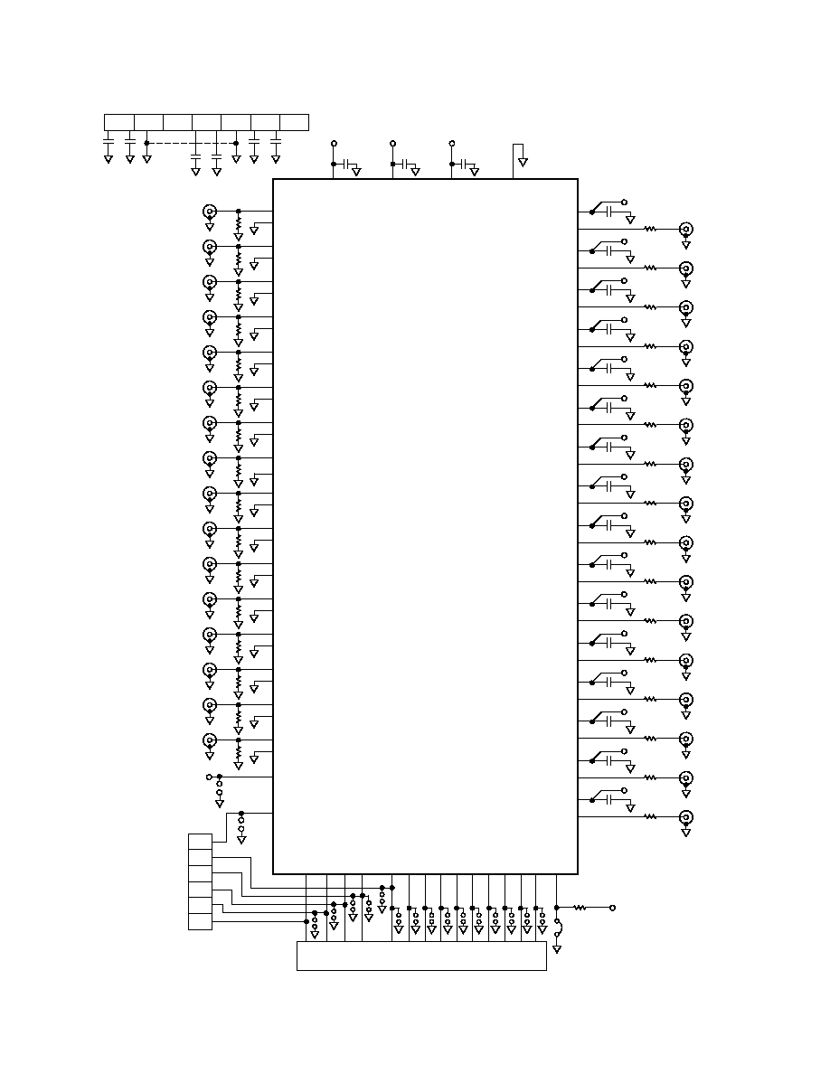
REV. A
AD8113
22
57,59
58
75
INPUT 00
INPUT 00
AGND
75
54
0.01 F
61
60
75
INPUT 01
INPUT 01
AGND
63
62
75
INPUT 02
INPUT 02
AGND
65
64
75
INPUT 03
INPUT 03
AGND
67
66
75
INPUT 04
INPUT 04
AGND
69
68
75
INPUT 05
INPUT 05
AGND
71
70
75
INPUT 06
INPUT 06
AGND
72
75
INPUT 07
INPUT 07
5
4
75
INPUT 08
INPUT 08
AGND
7
6
75
INPUT 09
INPUT 09
AGND
9
8
75
INPUT 10
INPUT 10
AGND
11
10
75
INPUT 11
INPUT 11
AGND
13
12
75
INPUT 12
INPUT 12
AGND
15
14
75
INPUT 13
INPUT 13
AGND
17
16
75
INPUT 14
INPUT 14
AGND
19
18
75
INPUT 15
INPUT 15
AGND
98
DATA OUT
96
DATA IN
P2-5
P2-4
P2-2
P2-3
P2-1
P2-6
RESET
DGND
CE
CLK
UPDATE
SER
/PAR
A0
A1
A2
D0
D1
D2
D3
D4
P3-1
P3-2
P3-3
P3-4
P3-5
P3-6
P3-7
P3-8
P3-9
P3-10
P3-11
P3-12
P3-13
P3-14
2,74 100
99
97
95 84
83
82 81 80 79 78 77 76
SERIAL MODE
JUMP
R33
20k
DV
CC
OUTPUT 00
0.01 F
20, 56
AV
EE
AV
EE
0.01 F
21, 55
AV
CC
AV
CC
0.01 F
1, 75
DV
CC
AD8113
DV
CC
DGND
NC
AV
EE
AGND AV
CC
NC
P1-1
+
+
+
P1-2
P1-3
P1-4
P1-5
P1-6
P1-7
0.1 F 10 F
0.1 F 10 F
0.1 F 10 F
JUMPER
3,73
AGND
R
R
R
NOTE
R = OPTIONAL 50 TERMINATOR RESISTORS
C = OPTIONAL SMOOTHING CAPACITOR
R
R
C
R
R
A3
R
R
R
R
R
R
R
R
R
94
NO CONNECT:
85-93
AV
CC
AV
CC
OUTPUT 00
53
75
52
0.01 F
OUTPUT 01
AV
EE
AV
EE
OUTPUT 01
51
75
50
0.01 F
OUTPUT 02
AV
CC
AV
CC
OUTPUT 02
49
75
48
0.01 F
OUTPUT 03
AV
EE
AV
EE
OUTPUT 03
47
75
46
0.01 F
OUTPUT 04
AV
CC
AV
CC
OUTPUT 04
45
75
44
0.01 F
OUTPUT 05
AV
EE
AV
EE
OUTPUT 05
43
75
42
0.01 F
OUTPUT 06
AV
CC
AV
CC
OUTPUT 06
41
75
40
0.01 F
OUTPUT 07
AV
EE
AV
EE
OUTPUT 07
39
75
38
0.01 F
OUTPUT 08
AV
CC
AV
CC
OUTPUT 08
37
75
36
0.01 F
OUTPUT 09
AV
EE
AV
EE
OUTPUT 09
35
75
34
0.01 F
OUTPUT 10
AV
CC
AV
CC
OUTPUT 10
33
75
32
0.01 F
OUTPUT 11
AV
EE
AV
EE
OUTPUT 11
31
75
30
0.01 F
OUTPUT 12
AV
CC
AV
CC
OUTPUT 12
29
75
28
0.01 F
OUTPUT 13
AV
EE
AV
EE
OUTPUT 13
27
75
26
0.01 F
OUTPUT 14
AV
CC
AV
CC
OUTPUT 14
25
75
24
0.01 F
OUTPUT 15
AV
EE
AV
EE
OUTPUT 15
23
22
AV
CC
DV
CC
Figure 13. Evaluation Board Schematic
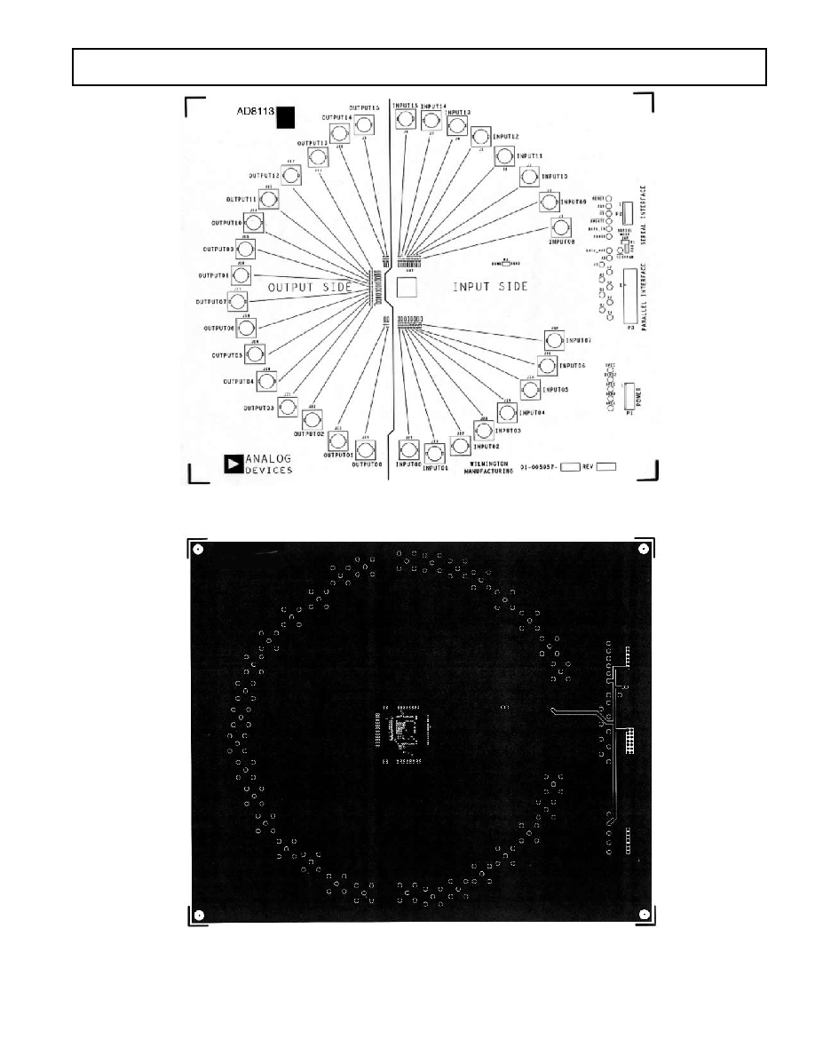
REV. A
AD8113
23
Figure 14. Component Side Silkscreen
Figure 15. Board Layout (Ground Plane)
REV. A
AD8113
24
Figure 16. Board Layout (Component Side)
Figure 17. Board Layout (Circuit Side)
REV. A
AD8113
25
Figure 18. Board Layout (Signal Layer)
Figure 19. Circuit Side Silkscreen
REV. A
AD8113
26
When the AD8113 is optimized for video applications, all signal
inputs and outputs are terminated with 75
resistors. Stripline
techniques are used to achieve a characteristic impedance on
the signal input and output lines, also of 75
. Figure 20 shows
a cross-section of one of the input or output tracks along with
the arrangement of the PCB layers. It should be noted that
unused regions of the four layers are filled up with ground planes.
As a result, the input and output traces, in addition to having
controlled impedances, are well shielded.
w = 0.008"
(0.2mm)
a = 0.008"
(0.2mm)
b = 0.0514"
(1.3mm)
h = 0.025"
(0.63mm)
t = 0.00135" (0.0343mm)
TOP LAYER
SIGNAL LAYER
POWER LAYER
BOTTOM LAYER
Figure 20. Cross Section of Input and Output Traces
The board has 32 BNC type connectors: 16 inputs and 16
outputs. The connectors are arranged in a crescent around the
device. As can be seen from Figure 16, this results in all 16 input
signal traces and all 16 output traces having the same length.
This is useful in tests such as all hostile crosstalk tests, where
the phase relationship and delay between signals need to be
maintained from input to output.
There are separate digital (logic) and analog supplies. DV
CC
should be at 5 V to be compatible with 5 V CMOS and TTL
logic. AV
CC
and AV
EE
can range from
±5 V to ±12 V depending
on the application.
As a general rule, each power supply pin (or group of adjacent
power supply pins) should be locally decoupled with a 0.01
µF
capacitor. If there is a space constraint, it is more important to
decouple analog power supply pins before digital power supply
pins. A 0.1
µF capacitor, located reasonably close to the pins,
can be used to decouple a number of power supply pins. Finally
a 10
µF capacitor should be used to decouple power supplies as
they come onto the board.
Controlling the Evaluation Board from a PC
The evaluation board includes Windows
®
based control software
and a custom cable that connects the board's digital interface
to the printer port of the PC. The wiring of this cable is shown in
Figure 21. The software requires Windows 3.1 or later. To install
the software, insert the disk labeled Disk #1 of 2 and run the file
called SETUP.EXE. Additional installation instructions will be
given on-screen. Before beginning installation, it is important
to terminate any other Windows applications that are running.
Audio signals are not as demanding on termination as are video
signals. Therefore, the input terminations can be removed and
changed. Likewise, the output series terminations can be shorted
or changed in value.
D-SUB 25-PIN (MALE)
14
1
25
13
PC
RESET
CLK
DATA IN
DGND
CE
UPDATE
MOLEX 0.100" CENTER
CRIMP TERMINAL HOUSING
1
6
EVALUATION BOARD
2
3
4
5
6
25
3
1
4
5
2
6
SIGNAL
CE
RESET
UPDATE
DATA IN
CLK
DGND
MOLEX
TERMINAL HOUSING
D-SUB-25
Figure 21. Evaluation Board/PC Connection Cable
When you launch the crosspoint control software, you will be
asked to select the printer port you are using. Most PCs have only
one printer port, usually called LPT1. However, some laptop
computers use the PRN port.
Figure 22 shows the main screen of the control software in its
initial reset state (all outputs off). Using the mouse, any input
can be connected with one or more outputs by simply clicking
on the appropriate radio buttons in the 16
× 16 on-screen array.
Each time a button is clicked on, the software automatically sends
and latches the required 80-bit data stream to the evaluation
board. An output can be turned off by clicking the appropriate
button in the off column. To turn off all outputs, click on Reset.
While the computer software only supports serial programming
via a PC's parallel port and the provided cable, the evaluation
board has a connector that can be used for parallel programming.
The
SER/PAR signal should be at a logic HIGH to use parallel
programming. There is no cable or software provided with the
evaluation board for parallel programming. These are left to the
user to provide.
The software offers volatile and nonvolatile storage of configura-
tions. For volatile storage, up to two configurations can be
stored and recalled using the Memory 1 and Memory 2 buffers.
These function in a fashion identical to the memory on a
pocket calculator. For nonvolatile storage of a configuration, the
Save Setup and Load Setup functions can be used. This stores
the configuration as a data file on disk.
Overshoot on PC Printer Ports' Data Lines
The data lines on some printer ports have excessive overshoot.
Overshoot on the pin that is used as the serial clock (Pin 6 on
the D-Sub-25 connector) can cause communication problems.
This overshoot can be eliminated by connecting a capacitor
from the CLK line on the evaluation board to ground. A pad
has been provided on the circuit side (C33) of the evaluation
board to allow this capacitor to be soldered into place. Depend-
ing upon the overshoot from the printer port, this capacitor may
need to be as large as 0.01
µF.
REV. A
AD8113
27
Figure 22. Screen Display and Control Software
AD8113
Parallel Port Selection
REV. A
28
C0217005/03(A)
AD8113
100-Lead Low Profile Quad Flat Package [LQFP]
(ST-100)
Dimensions shown in millimeters
TOP VIEW
(PINS DOWN)
1
25
26
51
50
75
76
100
14.00 BSC SQ
0.50 BSC
0.27
0.22
0.17
1.60 MAX
SEATING
PLANE
12
TYP
0.75
0.60
0.45
VIEW A
16.00 BSC SQ
12.00
REF
0.20
0.09
1.45
1.40
1.35
0.08 MAX
COPLANARITY
VIEW A
ROTATED 90 CCW
SEATING
PLANE
10
6
2
7
3.5
0
0.15
0.05
PIN 1
COMPLIANT TO JEDEC STANDARDS MS-026BED
OUTLINE DIMENSIONS
Revision History
Location
Page
4/03--Data Sheet changed from REV. 0 to REV. A.
New TPC 20 . . . . . . . . . . . . . . . . . . . . . . . . . . . . . . . . . . . . . . . . . . . . . . . . . . . . . . . . . . . . . . . . . . . . . . . . . . . . . . . . . . . . . . . . . . 12
Updated OUTLINE DIMENSIONS . . . . . . . . . . . . . . . . . . . . . . . . . . . . . . . . . . . . . . . . . . . . . . . . . . . . . . . . . . . . . . . . . . . . . . . 28
Document Outline
- FEATURES
- APPLICATIONS
- PRODUCT DESCRIPTION
- FUNCTIONAL BLOCK DIAGRAM
- SPECIFICATIONS
- TIMING CHARACTERISTICS (Serial)
- TIMING CHARACTERISTICS (Parallel)
- ABSOLUTE MAXIMUM RATINGS
- POWER DISSIPATION
- ORDERING GUIDE
- PIN FUNCTION DESCRIPTIONS
- PIN CONFIGURATION
- Typical Performance Characteristics
- THEORY OF OPERATION
- CALCULATION OF POWER DISSIPATION
- SHORT-CIRCUIT OUTPUT CONDITIONS
- APPLICATIONS
- Serial Programming
- Parallel Programming
- POWER-ON RESET
- SPECIFYING AUDIO LEVELS
- CREATING UNITY-GAIN CHANNELS
- VIDEO SIGNALS
- Power Considerations of Video Signals
- CREATING LARGER CROSSPOINT ARRAYS
- Multichannel Video and Audio
- CROSSTALK
- Types of Crosstalk
- Areas of Crosstalk
- Measuring Crosstalk
- Input and Output Crosstalk
- Effect of Impedances on Crosstalk
- PCB Layout
- Controlling the Evaluation Board from a PC
- Overshoot on PC Printer Ports Data Lines
- OUTLINE DIMENSIONS
- Revision History