 | ÐлекÑÑоннÑй компоненÑ: AD809 | СкаÑаÑÑ:  PDF PDF  ZIP ZIP |
Äîêóìåíòàöèÿ è îïèñàíèÿ www.docs.chipfind.ru
REV. A
Information furnished by Analog Devices is believed to be accurate and
reliable. However, no responsibility is assumed by Analog Devices for its
use, nor for any infringements of patents or other rights of third parties
which may result from its use. No license is granted by implication or
otherwise under any patent or patent rights of Analog Devices.
a
155.52 MHz Frequency Synthesizer
AD809
FEATURES
Frequency Synthesis to 155.52 MHz
19.44 MHz or 9.72 MHz Input
Reference Signal Select Mux
Single Supply Operation: +5 V or 5.2 V
Output Jitter: 2.0 Degrees RMS
Low Power: 90 mW
10 KH ECL/PECL Compatible Output
10 KH ECL/PECL/TTL/CMOS Compatible Input
Package: 16-Pin Narrow 150 Mil SOIC
One Technology Way, P.O. Box 9106, Norwood, MA 02062-9106, U.S.A.
Tel: 617/329-4700
World Wide Web Site: http://www.analog.com
Fax: 617/326-8703
© Analog Devices, Inc., 1997
155.52 Mbps ports. The AD809 can be applied to create the trans-
mit bit clock for one or more ports.
An input signal multiplexer supports loop-timed applications
where a 155.52 MHz transmit bit clock is recovered from the
155.52 Mbps received data.
The low jitter VCO, low power and wide operating temperature
range make the device suitable for generating a 155.52 MHz bit
clock for SONET/SDH/Fiber in the Loop systems.
The device has a low cost, on-chip VCO that locks to either
8
×
or 16
×
the frequency at the 19.44 MHz or 9.72 MHz input.
No external components are needed for frequency synthesis; how-
ever, the user can adjust loop dynamics through selection of a
damping factor capacitor whose value determines loop damping.
The AD809 design guarantees that the clock output frequency
will drift low (by roughly 20%) in the absence of a signal at the
input.
The AD809 consumes 90 mW and operates from a single power
supply at either +5 V or 5.2 V.
PRODUCT DESCRIPTION
The AD809 provides a 155.52 MHz ECL/PECL output clock from
either a 19.44 MHz or a 9.72 MHz TTL/CMOS/ECL/PECL refer-
ence frequency. The AD809 functionality supports a distributed
timing architecture, allowing a backplane or PCB 19.44 MHz or
9.72 MHz timing reference signal to be distributed to multiple
FUNCTIONAL BLOCK DIAGRAM
AUTO
SELECT
PFD
LOOP
FILTER
VCO
AUTO SELECT
DIVIDE BY 8/16
BW
ADJUST
MUX
CLKOUTN
(155MHz
PECL
OUTPUT)
CLKIN
TTL/CMOSIN
(155MHz)
MUX
CF1 CF2
AD809
15
1
2
10
12
13
7
8
5
4
CLKOUT
(19.44MHz
OR
9.72MHz)CLKINN
PECLIN
PECLINN
AD809SPECIFICATIONS
Parameter
Condition
Min
Typ
Max
Units
TRACKING AND CAPTURE RANGE
1
×
8 Synthesis
19.42
19.46
MHz
×
16 Synthesis
9.71
9.73
MHz
OUTPUT JITTER
×
8 Synthesis
1.6
2.9
Degrees RMS
×
16 Synthesis
1.6
2.9
Degrees RMS
JITTER TRANSFER
Bandwidth
200
kHz
Peaking
C
D
= 5.6 nF (
= 5)
0.08
dB
C
D
= 22 nF (
= 10)
0.02
dB
DUTY CYCLE TOLERANCE
×
8 or
×
16 Synthesis
Output Jitter
2.9 Degrees RMS
15
85
%
INPUT VOLTAGE LEVELS
PECL
Input Logic High, V
IH
@ CLKIN/N and
3.8
V
CC
Volts
Input Logic Low, V
IL
PECLIN/N Inputs
3.1
3.6
Volts
TTL
Input Logic High, V
IH
@ TTL/CMOSIN
2.0
Volts
Input Logic Low, V
IL
and MUX Inputs
0.8
Volts
OUTPUT VOLTAGE LEVELS
Referenced to V
CC
PECL
Output Logic High, V
OH
1.2
1.0
0.7
Volts
Output Logic Low, V
OL
2.0
1.8
1.7
Volts
SYMMETRY (Duty Cycle)
×
8 Synthesis or
46
52
62
%
×
16 Synthesis
%
OUTPUT RISE/FALL TIMES 1.5
Rise Time (t
R
)
20%80%
1.1
1.5
ns
Fall Time (t
F
)
80%20%
1.1
1.5
ns
POWER SUPPLY VOLTAGE
V
MIN
to V
MAX
4.5
5.5
Volts
POWER SUPPLY CURRENT
17
26
mA
OPERATING TEMPERATURE RANGE
T
MIN
to T
MAX
40
+85
°
C
NOTES
1
Device design is guaranteed for operation over Capture Ranges and Tracking Ranges, however the device has wider capture and tracking ranges
(for both
×
8 and
×
16 synthesis).
Specifications subject to change without notice.
REV. A
2
(T
A
= T
MIN
to T
MAX
, V
S
= V
MIN
to V
MAX
, C
D
= 22 nF, unless otherwise noted)
ABSOLUTE MAXIMUM RATINGS*
Supply Voltage . . . . . . . . . . . . . . . . . . . . . . . . . . . . . . . . +12 V
Input Voltage (Pin 12 or Pin 13) . . . . . . . . . . . . . . V
CC
+ 0.6 V
Maximum Junction Temperature. . . . . . . . . . . . . . . . . +165
°
C
Storage Temperature Range . . . . . . . . . . . . . 65
°
C to +150
°
C
Lead Temperature Range (Soldering 10 sec) . . . . . . . . +300
°
C
ESD Rating (Human Body Model) . . . . . . . . . . . . . . . . 1500 V
*Stresses above those listed under "Absolute Maximum Ratings" may cause
permanent damage to the device. This is a stress rating only; functional operation
of the device at these or any other conditions above those indicated in the
operational section of this specification is not implied. Exposure to absolute
maximum rating conditions for extended periods may affect device reliability.
Thermal Characteristics:
16-Pin Narrow Body SOIC Package:
JA
= 110
°
C/W.
ORDERING GUIDE
Model
Temperature Range
Package Description
Package Option
AD809BR
40
°
C to +85
°
C
16-Pin Narrow Body SOIC
R-16A
AD809BR-REEL7
40
°
C to +85
°
C
750 Pieces, 7" Reel
R-16A
"ON" TIME
t
ON
OUTPUT 50%
(PINS 4 & 5)
PERIOD
SYMMETRY = (100
×
t
ON
/
)
Figure 1. Symmetry
AD809
REV. A
3
Table I.
MUX Input
Input Selected
TTL "0"
CLKIN/CLKINN
TTL "1"
PECLIN/PECLINN
Table II. Applying a PECL/ECL or CMOS/TTL Reference
Input to the AD809
Input Reference
AD809 Configuration
PECL/ECL Differential
Apply the valid PECLlevel reference
frequency to Pins 13 and 12.
AD809 frequency synthesizer ignores
the input at Pin 10.
TTL/CMOS
Apply the reference frequency to
Single-Ended
Pin 10.
Connect Pins 13 and 12 to AV
EE
(Pins 9 and 16). The AD809 senses
the common-mode signal at these pins
as less than valid PECL and selects the
TTL/CMOS input as active.
AD809 Phase Skew
The AD809 output is in phase with the input. The falling edge
at Pin 4, CLKOUTN, occurs 700 ps before the rising edge at
Pin 10, TTL/CMOSIN at 27
°
C. The phase skew remains rela-
tively constant over temperature. Refer to Table III for phase
skew data.
Table III. Phase Skew vs. Temperature
Skew (CLKOUTN, Pin 4, Relative to
Temperature
TTL/CMOSIN, Pin 10 Measured in
( C)
ps at Package Pins)
35
1000
20
950
0
850
10
750
30
700
50
600
70
450
80
450
90
350
100
250
PIN DESCRIPTIONS
Pin
No.
Mnemonic
Description
1
PECLINN
Differential 155 MHz Input
2
PECLIN
Differential 155 MHz Input
3
V
CC2
Digital V
CC
for PECL Outputs
4
CLKOUTN
Differential 155 MHz Output
5
CLKOUT
Differential 155 MHz Output
6
V
CC1
Digital V
CC
for Internal Logic
7
CF1
Loop Damping Capacitor
8
CF2
Loop Damping Capacitor
9
AV
EE
Analog V
EE
10
TTL/CMOSIN TTL/CMOS Reference Clock Input
11
AV
CC1
Analog V
CC
for PLL
12
CLKINN
PECL Differential Reference Clock Input
13
CLKIN
PECL Differential Reference Clock Input
14
AV
CC2
Analog V
CC
for Input Stage
15
MUX
Input Signal Mux Control Input
16
V
EE
Digital V
EE
PIN CONFIGURATION
14
13
12
11
16
15
10
9
8
1
2
3
4
7
6
5
TOP VIEW
(Not to Scale)
AD809
PECLINN
CLKIN
AV
CC2
MUX
V
EE
PECLIN
V
CC2
CLKOUTN
TTL/CMOSIN
AV
CC1
CLKINN
CLKOUT
V
CC1
CF1
CF2
AV
EE
WARNING!
ESD SENSITIVE DEVICE
CAUTION
ESD (electrostatic discharge) sensitive device. Electrostatic charges as high as 4000 V readily
accumulate on the human body and test equipment and can discharge without detection.
Although the AD809 features proprietary ESD protection circuitry, permanent damage may
occur on devices subjected to high energy electrostatic discharges. Therefore, proper ESD
precautions are recommended to avoid performance degradation or loss of functionality.
AD809
REV. A
4
DEFINITION OF TERMS
Maximum, Minimum and Typical Specifications
Specifications for every parameter are derived from statistical
analyses of data taken on multiple devices from multiple wafer
lots. Typical specifications are the mean of the distribution of
the data for that parameter. If a parameter has a maximum (or a
minimum), that value is calculated by adding to (or subtracting
from) the mean six times the standard deviation of the distribu-
tion. This procedure is intended to tolerate production varia-
tions: if the mean shifts by 1.5 standard deviations, the remaining
4.5 standard deviations still provide a failure rate of only 3.4
parts per million. For all tested parameters, the test limits are
guardbanded to account for tester variation to thus guarantee
that no device is shipped outside of data sheet
specifications.
Capture and Tracking Range
This is the range of input data rates over which the AD809 will
remain in lock.
Jitter
This is the dynamic displacement of digital signal edges from
their long term average positions, measured in degrees rms.
Jitter on the input clock causes jitter on the synthesized clock.
Output Jitter
This is the jitter on the synthesized clock (OUTPUT, OUTPUT),
in degrees rms.
Jitter Transfer
The AD809 exhibits a low-pass filter response to jitter applied
to its input data.
Bandwidth
This describes the frequency at which the AD809 attenuates
sinusoidal input jitter by 3 dB.
Peaking
This describes the maximum jitter gain of the AD809 in dB.
Damping Factor,
Damping factor,
describes the compensation of the second or-
der PLL. A larger value of
corresponds to more damping and
less peaking in the jitter transfer function.
Duty Cycle Tolerance
The AD809 exhibits a duty cycle tolerance that is measured
by applying an input signal (nominal input frequency) with a
known duty cycle imbalance and measuring the
×
8 or
×
16
output frequency.
Symmetry-Recovered Clock Duty Cycle
Symmetry is calculated as (100
×
on time)/period, where on time
equals the time that the clock signal is greater than the midpoint
between its "0" level and its "1" level.
Typical Characteristic Curves
POPULATION Devices
RMS JITTER Degrees
1200
1000
0
More
1.8
800
600
400
200
0.2 0.4 0.6 0.8 1.0 1.2 1.4 1.6
2.0 2.2 2.4 2.6 2.8 3.0 3.2 3.4
100
90
80
70
60
50
40
30
20
10
0
CUMULATIVE %
AD809 FREQUENCY SYNTHESIZER
JITTER DISTRIBUTION MATRIX
75 DEVICES (3 LOTS)
[ECL, TTL]
×
[
×
8,
×
16]
×
[RISE, FALL]
×
[+4.5V, +5.0V, +5.5V]
×
[40
°
C, +25
°
C, +85
°
C]
THIS CHART DESCRIBES THE
AD809 OUTPUT JITTER
SPECIFICATION OVER MANY
CONDITIONS. THE DATA
REPRESENTED ARE TAKEN
WITH RESPECT TO THE RISING
AND FALLING EDGES, FOR
EACH FREQUENCY RANGE,
LOCKED TO EITHER TTL OR
ECL INPUT, OVER ALL
TEMPERATURE AND SUPPLY
CONDITIONS.
0.0
FREQUENCY
CUMULATIVE %
Figure 2. Jitter Histogram
INPUT DUTY CYCLE %
RMS JITTER Degrees
1.9
1.3
1.0
0
100
10
20
30
40
50
60
70
80
90
1.8
1.2
1.1
1.6
1.4
1.7
1.5
T
A
= +25
°
C
V
CC
= +5V
19.44MHz
9 72MHz
Figure 3. Jitter vs. Input Duty Cycle
AD809
REV. A
5
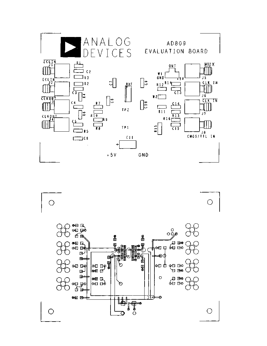
USING THE AD809
Ground Planes
Use of one ground plane for connections to both analog and
digital grounds is recommended.
Power Supply Connections
Use of a 10
µ
F capacitor between V
CC
and ground is recom-
mended. Care should be taken to isolate the +5 V power trace
to V
CC2
(Pin 3). The V
CC2
pin is used inside the device to pro-
vide the CLKOUT/CLKOUTN signals.
Use of a trace connecting Pin 14 and Pin 6 (AV
CC2
and V
CC1
respectively) is recommended. Use of 0.1
µ
F capacitors between
IC power supply and ground is recommended. Power supply
decoupling should take place as close to the IC as possible.
Refer to the schematic, Figure 5, for advised connections.
Transmission Lines
Use of 50
transmission lines are recommended for PECL
inputs.
Terminations
Termination resistors should be used for PECL input signals.
Metal, thick film, 1% tolerance resistors are recommended.
Termination resistors for the PECL input signals should be
placed as close as possible to the PECL input pins.
Connections from the power supply to load resistors for input
and output signals should be individual, not daisy chained. This
will avoid crosstalk on these signals.
Loop Damping Capacitor, C
D
A ceramic capacitor may be used for the loop damping capaci-
tor. A 22 nF capacitor provides a damping factor of 10.
Synthesizer Input
TTL/CMOSIN
Synthesizer Input
CLKIN/CLKINN
PECL INPUT
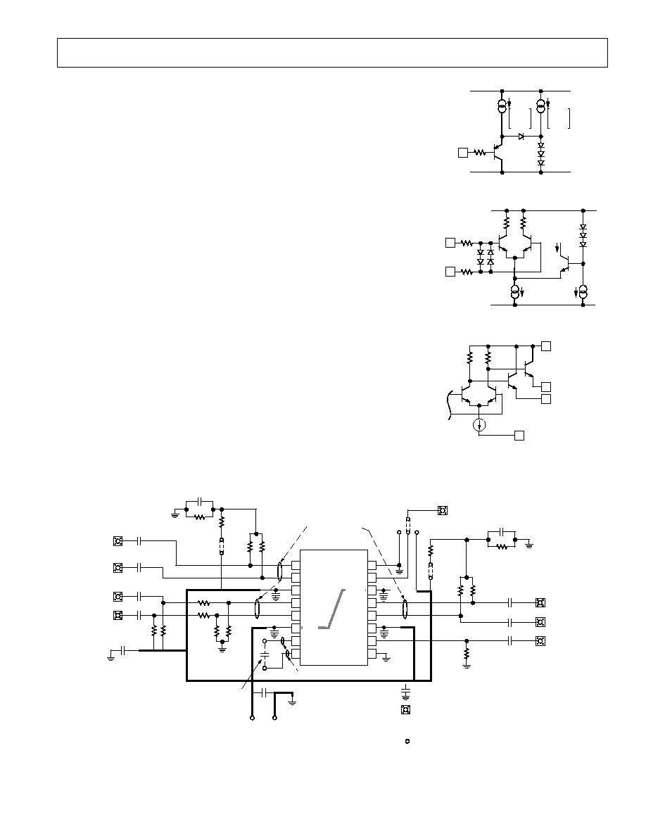
PLL Differential
Output Stage
CLKOUT/CLKOUTN
2*I
TTL
80µA
OR
0µA
2*I
TTL
80µA
OR
0µA
500
V
CC1
V
EE
V
CC2
DIFFERENTIAL
OUTPUT
V
EE
2.6mA
460
460
500
7.5k
7.5k
I
TTL
V
CC1
V
EE
500
40µA
40µA
Figure 4. Simplified Schematics
V
EE
14
13
12
11
16
15
10
9
8
1
2
3
4
7
6
5
V
CC2
CLKOUTN
CLKOUT
CF1
CF2
MUX
CLKIN
CLKINN
AV
CC1
TTL/CMOSIN
AV
EE
GND
J5
MUX
EXT
+5V
AD809
16-PIN SOIC
SOLDERED TO BOARD
C1
0.1µF
R6
3.65k
R5
301
R2
49.9
R1
49.9
JUMPER
W2
R16
301
V
CC1
AV
CC2
GUARD RING
+5V
GND
C11
10µF
TP4
TP3
R7 100
R8 100
R12
154
R11
154
CD
TP1
TP2
C8
C7
C6
0.1µF
R4
100
R3
100
VECTOR PINS SPACED FOR THROUGH-HOLE
CAPACITOR ON VECTOR CUPS.
COMPONENT SHOWN FOR REFERENCE ONLY.
C5 0.1µF
J3
J4
C4 0.1µF
ECL INN
ECL IN
CLKOUTN
CLKOUT
J2
C3 0.1µF
J1
C2 0.1µF
50
STRIP LINE
EQUAL LENGTH
JUMPER
W1
JUMPER
W3
R15
49.9
R14
49.9
J6
CLKIN
J7
CLKINN
C13 0.1µF
C14 0.1µF
J8
CMOS/TTL IN
C15 0.1µF
R13
49.9
C12
0.1µF
R17
3.65k
NOTE:
C7C10 ARE 0.1µF BYPASS CAPACITORS
RIGHT ANGLE SMA CONNECTOR
OUTER SHELL TO GND PLANE
ALL RESISTORS ARE 1% 1/8 WATT SURFACE MOUNT
TPx
TEST POINTS ARE VECTOR PINS
C9
C10
PECLINN
PECLIN
Figure 5. Evaluation Board Schematic
AD809
REV. A
6
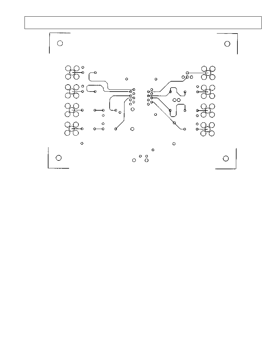
Figure 7. Evaluation Board: Solder Side
Figure 6. Evaluation Board: Component Side
AD809
REV. A
7
Figure 8. Evaluation Board: INT2
AD809
REV. A
8
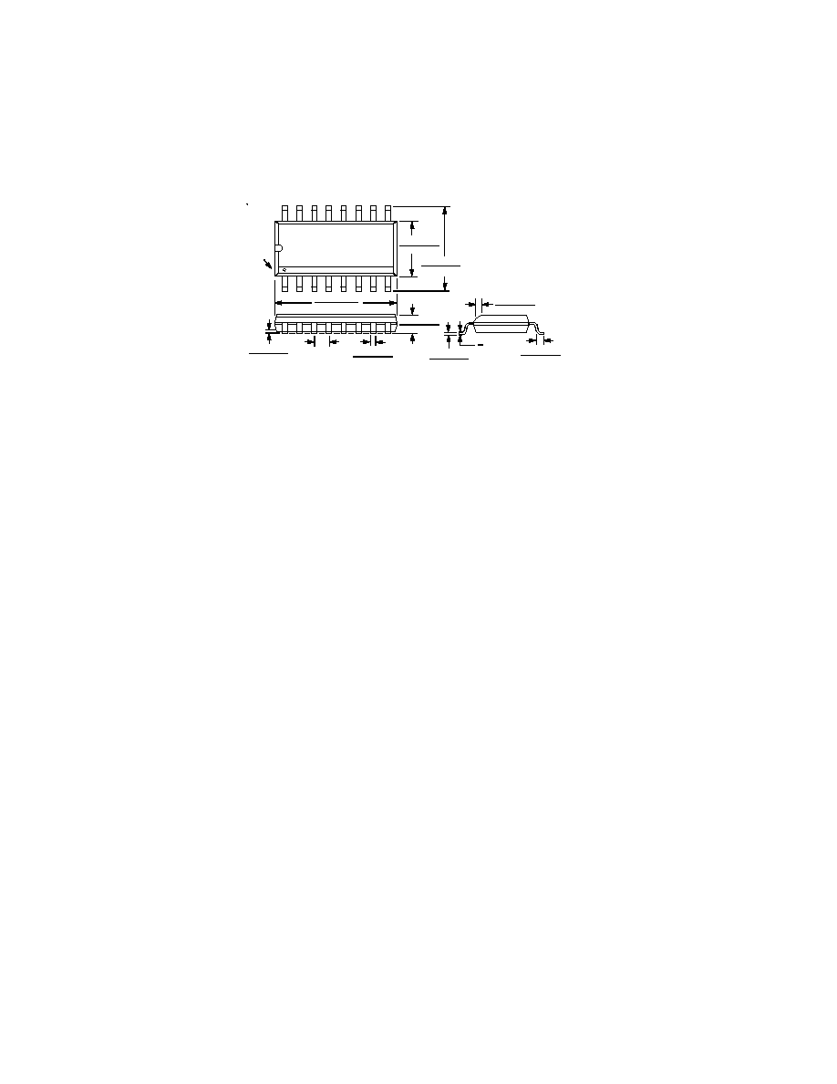
OUTLINE DIMENSIONS
Dimensions shown in inches and (mm).
16-Lead Small Outline IC Package
(R-16A)
PIN 1
0.1574 (4.00)
0.1497 (3.80)
0.2440 (6.20)
0.2284 (5.80)
1
16
9
8
0.0500 (1.27)
0.0160 (0.41)
8
°
0
°
0.0196 (0.50)
0.0099 (0.25)
x 45
°
0.0099 (0.25)
0.0075 (0.19)
0.0192 (0.49)
0.0138 (0.35)
0.0500
(1.27)
BSC
0.0688 (1.75)
0.0532 (1.35)
0.0098 (0.25)
0.0040 (0.10)
0.3937 (10.00)
0.3859 (9.80)
C2045a21/97
PRINTED IN U.S.A.