
FUNCTIONAL BLOCK DIAGRAM
1
2
3
4
5
6
7
8
AD783
V
CC
IN
COMMON
NC
OUT
S/H
NC
V
EE
NC = NO CONNECT
X1
REV. A
Information furnished by Analog Devices is believed to be accurate and
reliable. However, no responsibility is assumed by Analog Devices for its
use, nor for any infringements of patents or other rights of third parties
which may result from its use. No license is granted by implication or
otherwise under any patent or patent rights of Analog Devices.
a
Complete Very High Speed
Sample-and-Hold Amplifier
AD783*
One Technology Way, P.O. Box 9106, Norwood, MA 02062-9106, U.S.A.
Tel: 617/329-4700
Fax: 617/326-8703
FEATURES
Acquisition Time to 0.01%: 250 ns Typical
Low Power Dissipation: 95 mW
Low Droop Rate: 0.02 V/ s
Fully Specified and Tested Hold Mode Distortion
Total Harmonic Distortion: �85 dB
Aperture Jitter: 50 ps Maximum
Internal Hold Capacitor
Self-Correcting Architecture
8-Pin Mini Cerdip and SOIC Packages
PRODUCT DESCRIPTION
The AD783 is a high speed, monolithic sample-and-hold
amplifier (SHA). The AD783 offers a typical acquisition time
of 250 ns to 0.01%. The AD783 is specified and tested for hold
mode total harmonic distortion with input frequencies up to
100 kHz. The AD783 is configured as a unity gain amplifier
and uses a patented self-correcting architecture that minimizes
hold mode errors and ensures accuracy over temperature. The
AD783 is self-contained and requires no external components
or adjustments.
The AD783 retains the held value with a droop rate of 0.02
�
V/
�
s. Excellent linearity and hold mode dc and dynamic perfor-
mance make the AD783 ideal for high speed 12- and 14-bit
analog-to-digital converters.
The AD783 is manufactured on Analog Devices' ABCMOS
process which merges high performance, low noise bipolar
circuitry with low power CMOS to provide an accurate, high
speed, low power SHA.
The J grade device is specified for operation from 0
�
C to +70
�
C
and the A grade from �40
�
C to +85
�
C. The J and A grades are
available in 8-pin cerdip and SOIC packages. The military
temperature range version is specified for operation from �55
�
C
to +125
�
C and is available in an 8-pin cerdip package. For
details refer to the Analog Devices Military Products Databook or
AD783/883B data sheet.
*Protected by U.S. Patent Number 4,962,325.
PRODUCT HIGHLIGHTS
1. Fast acquisition time (250 ns), low aperture jitter (20 ps) and
fully specified hold mode distortion make the AD783 an
ideal SHA for sampling systems.
2. Low droop (0.02
�
V/
�
s) and internally compensated hold
mode error result in superior system accuracy.
3. Low power (95 mW typical), complete functionality and
small size make the AD783 an ideal choice for a variety of
high performance applications.
4. The AD783 requires no external components or adjustments.
5. The AD783 is an excellent choice as a front-end SHA for
high speed analog-to-digital converters such as the AD671,
AD7586, AD674B, AD774B, AD7572 and AD7672.
6. Fully specified and tested hold mode distortion guarantees
the performance of the SHA in sampled data systems.

REV. A
�2�
AD783�SPECIFICATIONS
DC SPECIFICATIONS
AD783J/A
Parameter
Min
Typ
Max
Units
SAMPLING CHARACTERISTICS
Acquisition Time
5 V Step to 0.01%
250
375
ns
5 V Step to 0.1%
200
350
ns
Small Signal Bandwidth
15
MHz
Full Power Bandwidth
2
MHz
HOLD CHARACTERISTICS
Effective Aperture Delay (+25
�
C)
�30
15
30
ns
Aperture Jitter (+25
�
C)
20
50
ps
Hold Settling (to 1 mV, +25
�
C)
150
200
ns
Droop Rate
0.02
1
�
V/
�
s
Feedthrough (+25
�
C)
(V
IN
=
�
2.5 V, 500 kHz)
�80
dB
ACCURACY CHARACTERISTICS
1
Hold Mode Offset
�5
0
+5
mV
Hold Mode Offset Drift
10
�
V/
�
C
Sample Mode Offset
50
200
mV
Nonlinearity
�
0.005
% FS
Gain Error
�
0.03
�
0.1
% FS
OUTPUT CHARACTERISTICS
Output Drive Current
�5
+5
mA
Output Resistance, DC
0.3
0.6
Total Output Noise (DC to 5 MHz)
150
�
V rms
Sampled DC Uncertainty
85
�
V rms
Hold Mode Noise (DC to 5 MHz)
125
�
V rms
Short Circuit Current
Source
20
mA
Sink
13
mA
INPUT CHARACTERISTICS
Input Voltage Range
�2.5
+2.5
V
Bias Current
100
250
nA
Input Impedance
10
M
Input Capacitance
2
pF
DIGITAL CHARACTERISTICS
Input Voltage Low
0.8
V
Input Voltage High
2.0
V
Input Current High (V
IN
= 5 V)
2
10
�
A
POWER SUPPLY CHARACTERISTICS
Operating Voltage Range
�
4.75
�
5
�
5.25
V
Supply Current
9.5
17
mA
+PSRR (+5 V
�
5%)
45
65
dB
�PSRR (�5 V
�
5%)
45
65
dB
Power Consumption
95
175
mW
TEMPERATURE RANGE
Specified Performance (J)
0
+70
�
C
Specified Performance
(A)
�40
+85
�
C
NOTES
1
Specified and tested over an input range of
�
2.5 V.
Specifications subject to change without notice.
(T
MIN
to T
MAX
with V
CC
= +5 V 5%, V
EE
= �5 V 5%, C
L
= pF, unless otherwise noted)
AD783
REV. A
�3�
HOLD MODE AC SPECIFICATIONS
AD783J/A
Parameter
Min
Typ
Max
Units
TOTAL HARMONIC DISTORTION
f
IN
= 100 kHz
�85
�80
dB
f
IN
= 500 kHz
�72
dB
SIGNAL-TO-NOISE AND DISTORTION
f
IN
= 100 kHz
77
dB
f
IN
= 500 kHz
70
dB
INTERMODULATION DISTORTION
(F1 = 99 kHz, F2 = 100 kHz)
Second Order Products
�80
dB
Third Order Products
�85
dB
NOTES
1
f
IN
amplitude = 0 dB and f
SAMPLE
= 300 kHz unless otherwise indicated.
Specifications subject to change without notice.
(T
MIN
to T
MAX
with V
CC
= +5 V 5%, V
EE
= �5 V 5%, C
L
= 50 pF, unless otherwise noted)
ABSOLUTE MAXIMUM RATINGS*
With
Spec
Respect to
Min
Max
Units
V
CC
COM
�0.5
+6.5
V
V
EE
COM
�6.5
+0.5
V
Analog Input
COM
�6.5
+6.5
V
Digital Input
COM
�0.5
+6.5
V
Output Short Circuit to
Ground, V
CC
, or V
EE
Indefinite
Maximum Junction
Temperature
+175
�
C
Storage
�65
+150
�
C
Lead Temperature
(10 sec max)
+300
�
C
*Stresses above those listed under "Absolute Maximum Ratings" may cause
permanent damage to the device. This is a stress rating only and functional
operation of the device at these or any other conditions above those indicated in the
operational section of this specification is not implied.
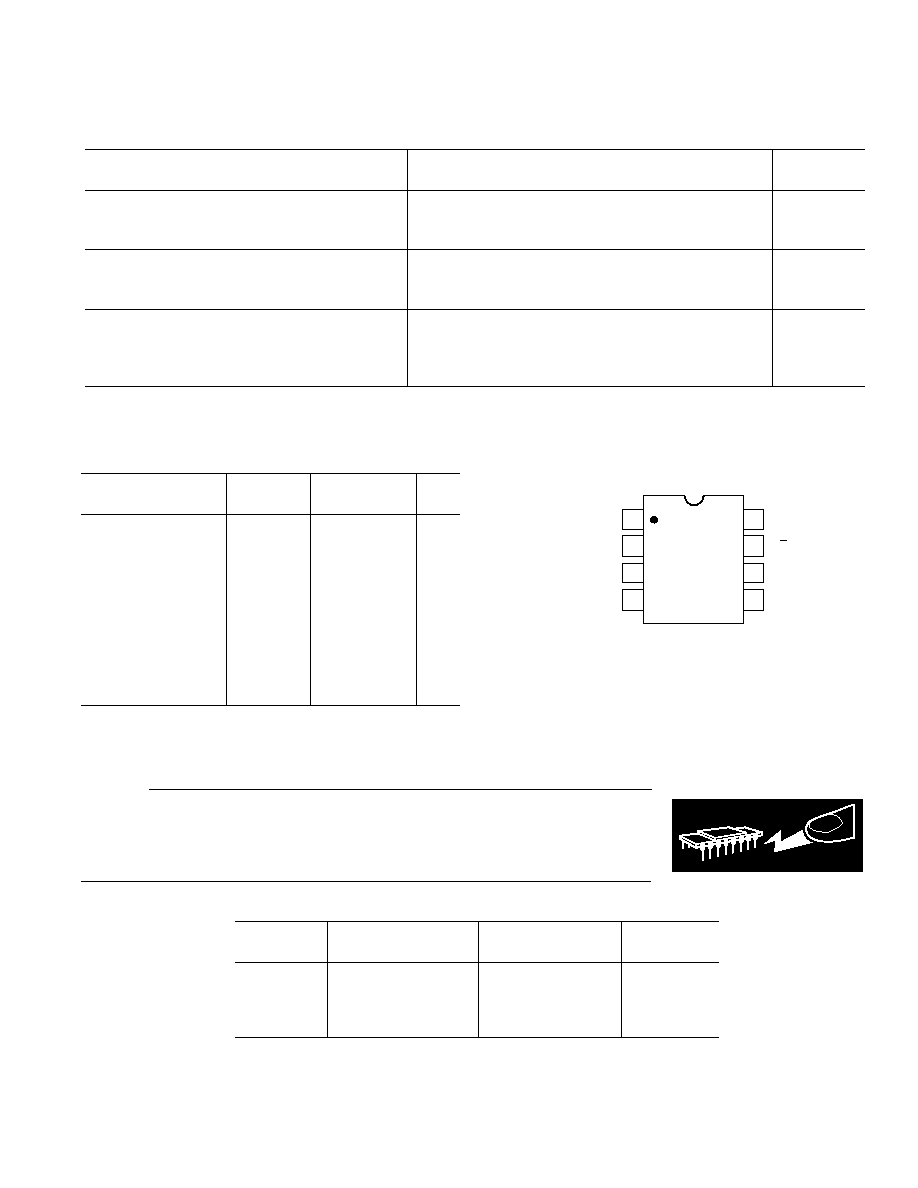
PIN CONFIGURATION
1
2
3
4
8
7
6
5
TOP VIEW
(Not to Scale)
AD783
V
CC
IN
COMMON
NC
OUT
NC
V
EE
S/H
NC = NO CONNECT
WARNING!
ESD SENSITIVE DEVICE
CAUTION
ESD (electrostatic discharge) sensitive device. Electrostatic charges as high as 4000 V readily
accumulate on the human body and test equipment and can discharge without detection.
Although the AD783 features proprietary ESD protection circuitry, permanent damage may
occur on devices subjected to high energy electrostatic discharges. Therefore, proper ESD
precautions are recommended to avoid performance degradation or loss of functionality.
ORDERING GUIDE
Temperature
Package
Model
1
Range
Description
Options
2
AD783JQ
0
�
C to +70
�
C
8-Pin Cerdip
Q-8
AD783AQ
�40
�
C to +85
�
C
8-Pin Cerdip
Q-8
AD783JR
0
�
C to +70
�
C
8-Pin SOIC
R-8
AD783AR
�40
�
C to +85
�
C
8-Pin SOIC
R-8
NOTES
1
For details on grade and package offerings screened in accordance with MIL-STD-883, refer to the
1
Analog Devices Military Products Databook or current AD783/883B data sheet.
2
Q = Cerdip, R = SOIC.

AD783�Typical Characteristics
REV. A
�4�
0
1M
30
10
1
40
50
60
100k
10k
1k
100
FREQUENCY � Hz
PSRR � dB
V+
V�
Power Supply Rejection Ratio vs. Frequency
200
�200
�100
�150
�2.5
0
�50
50
100
150
+2.5
0
INPUT VOLTAGE � V
BIAS CURRENT � nA
Bias Current vs. Input Voltage
10.0
0.001
0
150
1.0
0.01
25
0.1
125
100
75
50
TEMPERATURE �
�
C
DROOP RATE �
�
V/
�
s
Droop Rate vs. Temperature, V
IN
= 0 V
0
0
5
300
200
1
250
4
3
2
INPUT STEP � V
ACQUISITION TIME � ns
Acquisition Time (to 0.01%) vs. Input Step Size
AD783
REV. A
�5�
DEFINITIONS OF SPECIFICATIONS
Acquisition Time--The length of time that the SHA must
remain in the sample mode in order to acquire a full-scale input
step to a given level of accuracy.
Small Signal Bandwidth--The frequency at which the held
output amplitude is 3 dB below the input amplitude, under an
input condition of a 100 mV p-p sine wave.
Full Power Bandwidth--The frequency at which the held
output amplitude is 3 dB below the input amplitude, under an
input condition of a 5 V p-p sine wave.
Effective Aperture Delay--The difference between the switch
delay and the analog delay of the SHA channel. A negative
number indicates that the analog portion of the overall delay is
greater than the switch portion. This effective delay represents
the point in time, relative to the hold command, that the input
signal will be sampled.
Aperture Jitter--The variations in aperture delay for
successive samples. Aperture jitter puts an upper limit on the
maximum frequency that can be accurately sampled.
Hold Settling Time--The time required for the output to
settle to within a specified level of accuracy of its final held value
after the hold command has been given.
Droop Rate--The drift in output voltage while in the hold
mode.
Feedthrough--The attenuated version of a changing input
signal that appears at the output when the SHA is in the hold
mode.
Hold Mode Offset--The difference between the input signal
and the held output. This offset term applies only in the hold
mode and includes the error caused by charge injection and all
other internal offsets. It is specified for an input of 0 V.
Sample Mode Offset--The difference between the input and
output signals when the SHA is in the sample mode.
Nonlinearity--The deviation from a straight line on a plot of
input vs. (held) output as referenced to a straight line drawn
between endpoints, over an input range of �2.5 V and +2.5 V.
Gain Error--Deviation from a gain of +1 on the transfer
function of input vs. held output.
Power Supply Rejection Ratio--A measure of change in the
held output voltage for a specified change in the positive or
negative supply.
Sampled DC Uncertainty--The internal rms SHA noise that
is sampled onto the hold capacitor.
Hold Mode Noise--The rms noise at the output of the SHA
while in the hold mode, specified over a given bandwidth.
Total Output Noise--The total rms noise that is seen at the
output of the SHA while in the hold mode. It is the rms
summation of the sampled dc uncertainty and the hold mode
noise.
Output Drive Current--The maximum current the SHA can
source (or sink) while maintaining a change in hold mode offset
of less than 2.5 mV.
Signal-To-Noise and Distortion (S/N+D) Ratio--S/N+D is
the ratio of the rms value of the measured input signal to the
rms sum of all other spectral components below the Nyquist
frequency, including harmonics but excluding dc. The value for
S/N+D is expressed in decibels.
Total Harmonic Distortion (THD)--THD is the ratio of the
rms sum of the first six harmonic components to the rms value
of the measured input signal and is expressed in decibels.
Intermodulation Distortion (IMD)--With inputs consisting
of sine waves at two frequencies, fa and fb, any device with
nonlinearities will create distortion products, of order (m+n), at
sum and difference frequency of mfa
�
nfb, where m, n = 0, 1, 2,
3. . . . Intermodulation terms are those for which m or n is not
equal to zero. For example, the second order terms are (fa+fb)
and (fa�fb), and the third order terms are (2fa+fb), (2fa�fb),
(fa+2fb) and (fa�2fb). The IMD products are expressed as the
decibel ratio of the rms sum of the measured input signals to the
rms sum of the distortion terms. The two signals are of equal
amplitude, and peak value of their sums is �0.5 dB from full
scale. The IMD products are normalized to a 0 dB input signal.
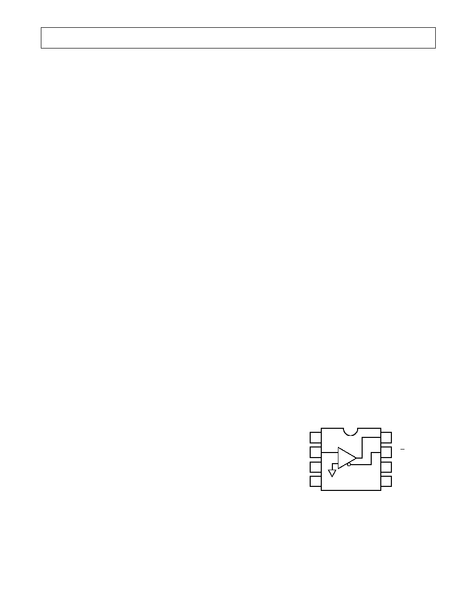
FUNCTIONAL DESCRIPTION
The AD783 is a complete, high speed sample-and-hold
amplifier that provides high speed sampling to 12-bit accuracy
in 250 ns.
The AD783 is completely self-contained, including an on-chip
hold capacitor, and requires no external components or adjust-
ments to perform the sampling function. Both input and output
are treated as a single-ended signal, referred to common.
The AD783 utilizes a proprietary circuit design which includes a
self-correcting architecture. This sample-and-hold circuit
corrects for internal errors after the hold command has been
given, by compensating for amplifier gain and offset errors, and
charge injection errors. Due to the nature of the design, the
SHA output in the sample mode is not intended to provide an
accurate representation of the input. However, in hold mode,
the internal circuitry is reconfigured to produce an accurately
held version of the input signal. Below is a block diagram of the
AD783.
1
2
3
4
5
6
7
8
AD783
V
CC
IN
COMMON
NC
OUT
S/H
NC
V
EE
NC = NO CONNECT
X1
Functional Block Diagram
AD783
REV. A
�6�
DYNAMIC PERFORMANCE
The AD783 is compatible with 12-bit A-to-D converters in
terms of both accuracy and speed. The fast acquisition time, fast
hold settling time and good output drive capability allow the
AD783 to be used with high speed, high resolution A-to-D
converters like the AD671 and AD7586. The AD783's fast
acquisition time provides high throughput rates for multichannel
data acquisition systems. Typically, the AD783 can acquire a
5 V step in less than 250 ns. Figure 1 shows the settling
accuracy as a function of acquisition time.
0.08
0.06
0.04
0.02
0
0
250
500
ACQUISITION TIME � ns
V ACQUISITION ACCURACY � %
OUT
Figure 1. V
OUT
Settling vs. Acquisition Time
The hold settling determines the required time, after the hold
command is given, for the output to settle to its final specified
accuracy. The typical settling behavior of the AD783 is 150 ns.
The settling time of the AD783 is sufficiently fast to allow the
SHA, in most cases, to directly drive an A-to-D converter
without the need for an added "start convert" delay.
HOLD MODE OFFSET
The dc accuracy of the AD783 is determined primarily by the
hold mode offset. The hold mode offset refers to the difference
between the final held output voltage and the input signal at the
time the hold command is given. The hold mode offset arises
from a voltage error introduced onto the hold capacitor by
charge injection of the internal switches. The nominal hold
mode offset is specified for a 0 V input condition. Over the in-
put range of �2.5 V to +2.5 V, the AD783 is also characterized
for an effective gain error and nonlinearity of the held value, as
shown in Figure 2. As indicated by the AD783 specifications,
the hold mode offset is very stable over temperature.
NONLINEARITY
GAIN ERROR
V , VOLTS
IN
�2.5
+2.5
+1
HOLD MODE OFFSET
�1
(V
OUT
HOLD � V
IN
), mV
Figure 2. Hold Mode Offset, Gain Error and Nonlinearity
For applications where it is important to obtain zero offset, the
hold mode offset may be nulled externally at the input to the
A-to-D converter. Adjustment of the offset may be accom-
plished through the A-to-D itself or by an external amplifier
with offset nulling capability (e.g., AD711). The offset will
change less than 0.5 mV over the specified temperature range.
SUPPLY DECOUPLING AND GROUNDING
CONSIDERATIONS
As with any high speed, high resolution data acquisition system,
the power supplies should be well regulated and free from
excessive high frequency noise (ripple). The supply connection
to the AD783 should also be capable of delivering transient
currents to the device. To achieve the specified accuracy and
dynamic performance, decoupling capacitors must be placed
directly at both the positive and negative supply pins to com-
mon. Ceramic type 0.1
�
F capacitors should be connected from
V
CC
and V
EE
to common.
ANALOG
P.S.
DIGITAL
P.S.
+5V
C
�5V
C
+5V
0.1
�
F
0.1
�
F
1
�
F
1
�
F
1
�
F
AD783
DIGITAL
DATA
OUTPUT
SIGNAL GROUND
INPUT
ANALOG-TO-DIGITAL
CONVERTER
Figure 3. Basic Grounding and Decoupling Diagram

AD783
REV. A
�7�
The AD783 does not provide separate analog and digital ground
leads as is the case with most A-to-D converters. The common
pin is the single ground terminal for the device. It is the refer-
ence point for the sampled input voltage and the held output
voltage and also the digital ground return path. The common
pin should be connected to the reference (analog) ground of the
A-to-D converter with a separate ground lead. Since the analog
and digital grounds in the AD783 are connected internally, the
common pin should also be connected to the digital ground,
which is usually tied to analog common at the A-to-D converter.
Figure 3 illustrates the recommended decoupling and grounding
practice.
NOISE CHARACTERISTICS
Designers of data conversion circuits must also consider the
effect of noise sources on the accuracy of the data acquisition
system. A sample-and-hold amplifier that precedes the A-to-D
converter introduces some noise and represents another source
of uncertainty in the conversion process. The noise from the
AD783 is specified as the total output noise, which includes
both the sampled wideband noise of the SHA in addition to the
band limited output noise. The total output noise is the rms
sum of the sampled dc uncertainty and the hold mode noise. A
plot of the total output noise vs. the equivalent input bandwidth
of the converter being used is given in Figure 4.
300
0
1k
10M
200
100
10k
1M
100k
FREQUENCY � Hz
OUTPUT NOISE �
�
V rms
Figure 4. RMS Noise vs. Input Bandwidth of ADC
DRIVING THE ANALOG INPUTS
For best performance, it is important to drive the AD783 analog
input from a low impedance signal source. This enhances the
sampling accuracy by minimizing the analog and digital cross-
talk. Signals which come from higher impedance sources (e.g.,
over 5 k
) will have a relatively higher level of crosstalk. For
applications where signals have high source impedance, an
operational amplifier buffer in front of the AD783 is required.
The AD711 (precision BiFET op amp) is recommended for
these applications.
HIGH FREQUENCY SAMPLING
Aperture jitter and distortion are the primary factors which limit
frequency domain performance of a sample-and-hold amplifier.
Aperture jitter modulates the phase of the hold command and
produces an effective noise on the sampled analog input. The
magnitude of the jitter induced noise is directly related to the
frequency of the input signal.
A graph showing the magnitude of the jitter induced error vs.
frequency of the input signal is given in Figure 5.
The accuracy in sampling high frequency signals is also
constrained by the distortion and noise created by the
sample-and-hold. The level of distortion increases with
frequency and reduces the "effective number of bits" of the
conversion.
Measurements of Figures 6 and 7 were made using a 14-bit
A/D converter with V
IN
= 5 V p-p and a sample frequency of
100 kSPS.
1%
1k
1M
0.1%
0.01%
10k
100k
FREQUENCY � Hz
APERTURE JITTER TYPICAL AT 20ps
1/2 BIT @
8 BITS
1/2 BIT @
10 BITS
1/2 BIT @
12 BITS
1/2 BIT @
14 BITS
Figure 5. Error Magnitude vs. Frequency
�65
�95
1M
�80
�90
1k
�85
100
�70
�75
100k
10k
FREQUENCY � Hz
THD � dB
Figure 6. Total Harmonic Distortion vs. Frequency
90
0
1M
20
10
10k
1k
30
40
50
60
70
80
100k
FREQUENCY � Hz
S/(N + D) � dB
Figure 7. Signal/(Noise and Distortion) vs. Frequency

AD783
REV. A
�8�
C1733�12�10/92
PRINTED IN U.S.A.
AD783 TO AD670 INTERFACE
The 15 MHz small signal bandwidth of the AD783 makes it a
good choice for undersampling applications. Figure 8 shows
the interface between the AD783 and the AD670 ADC, where
the AD783 samples the incoming IF signal. For this particular
application, the IF carrier was 10.7 MHz and the information
signal was a 5 kHz FSK-modulated tone. The sample-and-hold
signal is applied to the 8-bit AD670 ADC and then digitally
processed for analysis.
The CLKIN signal is connected directly to the S/H pin of the
AD783 and must comply with the acquisition and settling re-
quirements of the SHA. A delayed version of CLKIN is applied
to the R/W input of the AD670 in order to accommodate the
hold-mode settling requirements of the AD783. The 10
�
s con-
version speed of the AD670 combined with the 150 ns hold-
mode settling time of the AD783 result in a total system
throughput of 10.15
�
s.
By keeping the 10.7 MHz IF input to the AD783 at a low
amplitude, 255 mV p-p, the resultant distortion and jitter-
induced noise result in approximately 45 dB of dynamic range.
The AD670 can be conveniently configured such that its full-
scale input range is 255 mV in order to retain the full 8-bit
dynamic range of the converter. The maximum sample rate of
the AD670 is 10
�
s; therefore, to comply with the Nyquist
criteria the maximum information bandwidth is 50 kHz.
10k
2
7
8
AD670
+V
IN
HI
50
ANALOG
INPUT
CLK IN
10.7MHz
255mV p-p
+V
IN
LOW
�V
IN
HI
�V
IN
LOW
ONE -
SHOT
R/W
AD783
16
17
19
18
21
Figure 8. AD783 to AD670 Interface
AD783 to AD671 (12-Bit, 500 ns ADC) Interface
The AD783 to AD671 interface requires an op amp, a dual
flip-flop, and a monostable multivibrator or "one-shot." The
op amp amplifies the
�
2.5 V output of the AD783 to the
full-scale input of the AD671. Appropriate op amps include the
AD841 and AD845 (see the AD671 data sheet for additional
information). The flip-flops and one-shot are used to generate
the AD671 ENCODE pulse and the appropriately timed
AD783 S/H pulse.
A master sampling clock is tied to the clock input of flip-flop1
and the input of the one-shot. The D1 input of flip-flop1
should be tied high and the one-shot should be configured to
generate a pulse on a rising edge of the sampling clock. The ris-
ing edge of the sampling clock causes the Q1 output of the
flip-flop to go low placing the AD783 into hold mode. Simulta-
neously, a low going pulse is generated at the one-shot output.
The length of this pulse would usually be made long enough to
allow the output of the AD783 to settle (hold-mode settling
time), but because of the error-correcting ability of the AD671,
the length of this pulse may be reduced to approximately 200 ns.
The low going one-shot output is connected to the clock input
of flip-flop2. The D2 input of flip-flop2 is tied high. The rising
edge of the low going pulse toggles the Q2 output of flip-flop2 to
a high state. This output, which is tied to the ENCODE input of
the AD671, initiates a conversion of the buffered output signal
of the AD783. The AD671 issues the signal DAV when the con-
version is complete. The DAV signal is tied to the asynchronous
CLR1
and CLR2 inputs of both flip-flops. When DAV goes low,
the Q1 output goes high returning the AD783 to the sample or
acquisition mode. The Q2 output (ENCODE) returns low until
it is again triggered by the rising edge of the one-shot output.
V
IN
AD783
Q2
D1
D2
+5V
CLOCK
DAV
ENCODE
AIN
AD671
AD84X
ONE-
SHOT
Q1
CLR2
CLR1
Figure 9. AD783 to AD671 Interface
OUTLINE DIMENSIONS
Dimensions shown in inches and (mm).
8-Pin Cerdip (Q-8) Package
0.200
(5.08)
MAX
0.100 (2.54)
BSC
0.150
(3.81)
MIN
0.405 (10.29)
MAX
8
1
5
4
0.220 (5.59)
0.310 (7.87)
0.014 (0.36)
0.023 (0.58)
0.015 (0.38)
0.060 (1.52)
0.030 (0.76)
0.070 (1.78)
0.290 (7.37)
0.320 (8.13)
0.008 (0.204)
0.015 (0.381)
8-Pin SOIC (R-8) Package
1
4
5
8
0.050 (1.27)
BSC
0.188 (4.77)
0.198 (5.03)
0.150 (3.81)
0.158 (4.01)
0.224 (5.69)
0.248 (6.29)
0.014 (0.36)
0.022 (0.56)
0.195 (4.95)
0.205 (5.21)
0.089 (2.26)
0.107 (2.72)
0.018 (0.46)
0.034 (0.86)
0.007 (0.18)
0.015 (0.38)
0.005 (0.125)
0.011 (0.275)