 | ÐлекÑÑоннÑй компоненÑ: AD780 | СкаÑаÑÑ:  PDF PDF  ZIP ZIP |
Äîêóìåíòàöèÿ è îïèñàíèÿ www.docs.chipfind.ru
REV. B
Information furnished by Analog Devices is believed to be accurate and
reliable. However, no responsibility is assumed by Analog Devices for its
use, nor for any infringements of patents or other rights of third parties
which may result from its use. No license is granted by implication or
otherwise under any patent or patent rights of Analog Devices.
a
2.5 V/3.0 V
High Precision Reference
AD780
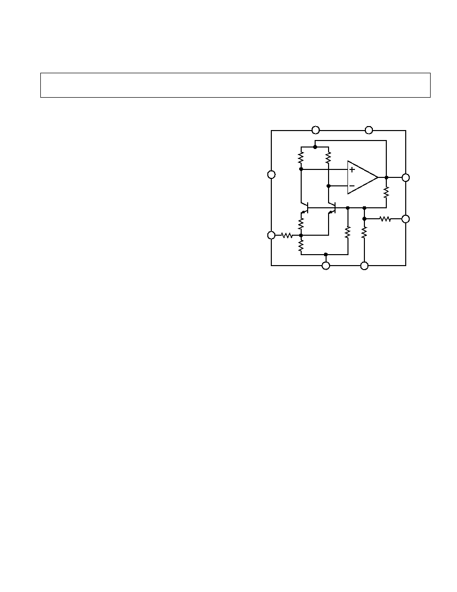
FUNCTIONAL BLOCK DIAGRAM
NC
TEMP
+V
IN
V
OUT
TRIM
GND
O/P SELECT
2.5V - NC
3.0V - GND
Q6
Q7
R10
R11
R5
R4
R14
R15
R16
R13
NC = NO CONNECT
NC
7
2
1
3
4
8
6
5
AD780
PRODUCT DESCRIPTION
The AD780 is an ultrahigh precision bandgap reference voltage
which provides a 2.5 V or 3.0 V output from inputs between
4.0 V and 36 V. Low initial error and temperature drift com-
bined with low output noise and the ability to drive any value of
capacitance make the AD780 the ideal choice for enhancing the
performance of high resolution ADCs and DACs and for any
general purpose precision reference application. A unique low
headroom design facilitates a 3.0 V output from a 5.0 V
± 10%
input, providing a 20% boost to the dynamic range of an ADC,
over performance with existing 2.5 V references.
The AD780 can be used to source or sink up to 10 mA and can
be used in series or shunt mode, thus allowing positive or nega-
tive output voltages without external components. This makes it
suitable for virtually any high performance reference application.
Unlike some competing references, the AD780 has no "region
of possible instability." The part is stable under all load condi-
tions when a 1
µF bypass capacitor is used on the supply.
A temperature output pin is provided on the AD780. This pro-
vides an output voltage that varies linearly with temperature, al-
lowing the AD780 to be configured as a temperature transducer
while providing a stable 2.5 V or 3.0 V output.
The AD780 is a pin-compatible performance upgrade for the
LT1019(A)2.5 and the AD680. The latter is targeted toward
low power applications.
The AD780 is available in three grades in plastic DIP, SOIC,
and cerdip packages. The AD780AN, AD780AR, AD780BN,
AD780BR, and AD780CR are specified for operation from 40
°C
to +85
°C.
FEATURES
Pin-Programmable 2.5 V or 3.0 V Output
Ultralow Drift: 3 ppm/ C max
High Accuracy: 2.5 V or 3.0 V 1 mV max
Low Noise: 100 nV/
Hz
Noise Reduction Capability
Low Quiescent Current: 1 mA max
Output Trim Capability
Plug-In Upgrade for Present References
Temperature Output Pin
Series or Shunt Mode Operation ( 2.5 V, 3.0 V)
PRODUCT HIGHLIGHTS
1. The AD780 provides a pin-programmable 2.5 V or 3.0 V
output from a 4 V to 36 V input.
2. Laser trimming of both initial accuracy and temperature
coefficients results in low errors over temperature without the
use of external components. The AD780BN has a maximum
variation of 0.9 mV from 40
°C to +85°C.
3. For applications requiring even higher accuracy, an optional
fine-trim connection is provided.
4. The AD780 noise is extremely low, typically 4
µV p-p from
0.1 Hz to 10 Hz and a wideband spectral noise density of
typically 100 nV/
Hz. This can be further reduced if desired,
by simply using two external capacitors.
5. The temperature output pin enables the AD780 to be config-
ured as a temperature transducer while providing a stable
output reference voltage.
One Technology Way, P.O. Box 9106, Norwood, MA 02062-9106, U.S.A.
Tel: 781/329-4700
World Wide Web Site: http://www.analog.com
Fax: 781/326-8703
© Analog Devices, Inc., 2000

AD780SPECIFICATIONS
AD780AN/AR
AD780CR
AD780BN/BR
Parameter
Min
Typ
Max
Min
Typ
Max
Min
Typ
Max
Unit
OUTPUT VOLTAGE
2.5 V Out
2.495
2.505
2.4985
2.5015
2.499
2.501
Volts
3.0 V Out
2.995
3.005
2.9950
3.0050
2.999
3.001
Volts
OUTPUT VOLTAGE DRIFT
1
40
°C to +85°C
7
7
3
ppm/
°C
55
°C to +125°C
20
20
ppm/
°C
LINE REGULATION
2.5 V Output, 4 V
+V
IN
36 V
T
MIN
to T
MAX
10
*
*
µV/V
3.0 V Output, 4.5 V
+V
IN
36 V
T
MIN
to T
MAX
10
*
*
µV/V
LOAD REGULATION, SERIES MODE
Sourcing 0 < I
OUT
< 10 mA
50
*
*
µV/mA
T
MIN
to T
MAX
75
*
*
µV/mA
Sinking 10 < I
OUT
< 0 mA
75
*
*
µV/mA
40
°C to +85°C
75
*
*
µV/mA
55
°C to +125°C
150
*
*
µV/mA
LOAD REGULATION, SHUNT MODE
I < I
SHUNT
< 10 mA
75
*
*
µV/mA
QUIESCENT CURRENT, 2.5 V SERIES MODE
2
40
°C to +85°C
0.75
1.0
*
*
*
*
mA
55
°C to +125°C
0.8
1.3
*
*
*
*
mA
MINIMUM SHUNT CURRENT
0.7
1.0
*
*
*
*
mA
OUTPUT NOISE
0.1 Hz to 10 Hz
4
*
*
*
*
µV p-p
Spectral Density, 100 Hz
100
*
*
*
*
nV/
Hz
LONG TERM STABILITY
3
20
*
*
±ppm/
1000 Hr
TRIM RANGE
4.0
*
*
±%
TEMPERATURE PIN
Voltage Output @ 25
°C
500
560
620
*
*
*
*
*
*
mV
Temperature Sensitivity
1.9
*
*
mV/
°C
Output Resistance
3
*
*
k
SHORT CIRCUIT CURRENT TO GROUND
30
*
*
mA
TEMPERATURE RANGE
Specified Performance (A, B, C)
40
+85
*
*
*
*
°C
Operating Performance (A, B, C)
4
55
+125
*
*
*
*
°C
Specified Performance (S)
55
+125
*
*
*
*
°C
Operating Performance (S)
55
+125
*
*
*
*
°C
NOTES
1
Maximum output voltage drift is guaranteed for all packages.
2
3.0 V mode typically adds 100
µA to the quiescent current. Also, Iq increases by 2 µA/V above an input voltage of 5 V.
3
The long term stability specification is noncumulative. The drift in subsequent 1000 hr. periods is significantly lower than in the first 1000 hr. period.
4
The operating temperature range is defined as the temperature extremes at which the device will still function. Parts may deviate from their specified performance
outside their specified temperature range.
*Same as AD780AN/AR specification.
Specifications subject to change without notice.
REV. B
2
(T
A
= +25 C, V
IN
= +5 V unless otherwise noted)
AD780
REV. B
3
ORDERING GUIDE
Initial
Temperature
Temperature
Package
Model
Error
Range
Coefficient
Options
AD780AN
5.0 mV
40
°C to +85°C
7 ppm/
°C
Plastic Dip
AD780AR
5.0 mV
40
°C to +85°C
7 ppm/
°C
SOIC
AD780AR-REEL7
5.0 mV
40
°C to +85°C
7 ppm/
°C
SOIC
AD780BN
1.0 mV
40
°C to +85°C
3 ppm/
°C
Plastic Dip
AD780BR
1.0 mV
40
°C to +85°C
3 ppm/
°C
SOIC
AD780BR-REEL
1.0 mV
40
°C to +85°C
3 ppm/
°C
SOIC
AD780BR-REEL7
1.0 mV
40
°C to +85°C
3 ppm/
°C
SOIC
AD780CR
1.5 mV
40
°C to +85°C
7 ppm/
°C
SOIC
AD780CR-REEL7
1.5 mV
40
°C to +85°C
7 ppm/
°C
SOIC
ABSOLUTE MAXIMUM RATINGS*
V
IN
to Ground . . . . . . . . . . . . . . . . . . . . . . . . . . . . . . . . . . 36 V
Trim Pin to Ground . . . . . . . . . . . . . . . . . . . . . . . . . . . . . 36 V
Temp Pin to Ground . . . . . . . . . . . . . . . . . . . . . . . . . . . . . 36 V
Power Dissipation (25
°C) . . . . . . . . . . . . . . . . . . . . . . 500 mW
Storage Temperature . . . . . . . . . . . . . . . . . . . 65
°C to +150°C
Lead Temperature (Soldering, 10 sec) . . . . . . . . . . . . . 300
°C
Output Protection: Output safe for indefinite short to ground
and momentary short to V
IN
.
ESD Classification . . . . . . . . . . . . . . . . . . . . . Class 1 (1000 V)
*Stresses above those listed under Absolute Maximum Ratings may cause perma-
nent damage to the device. This is a stress rating only; functional operation of the
device at these or any conditions above those indicated in the operational specifi-
cation is not implied. Exposure to absolute maximum specifications for extended
periods may affect device reliability.
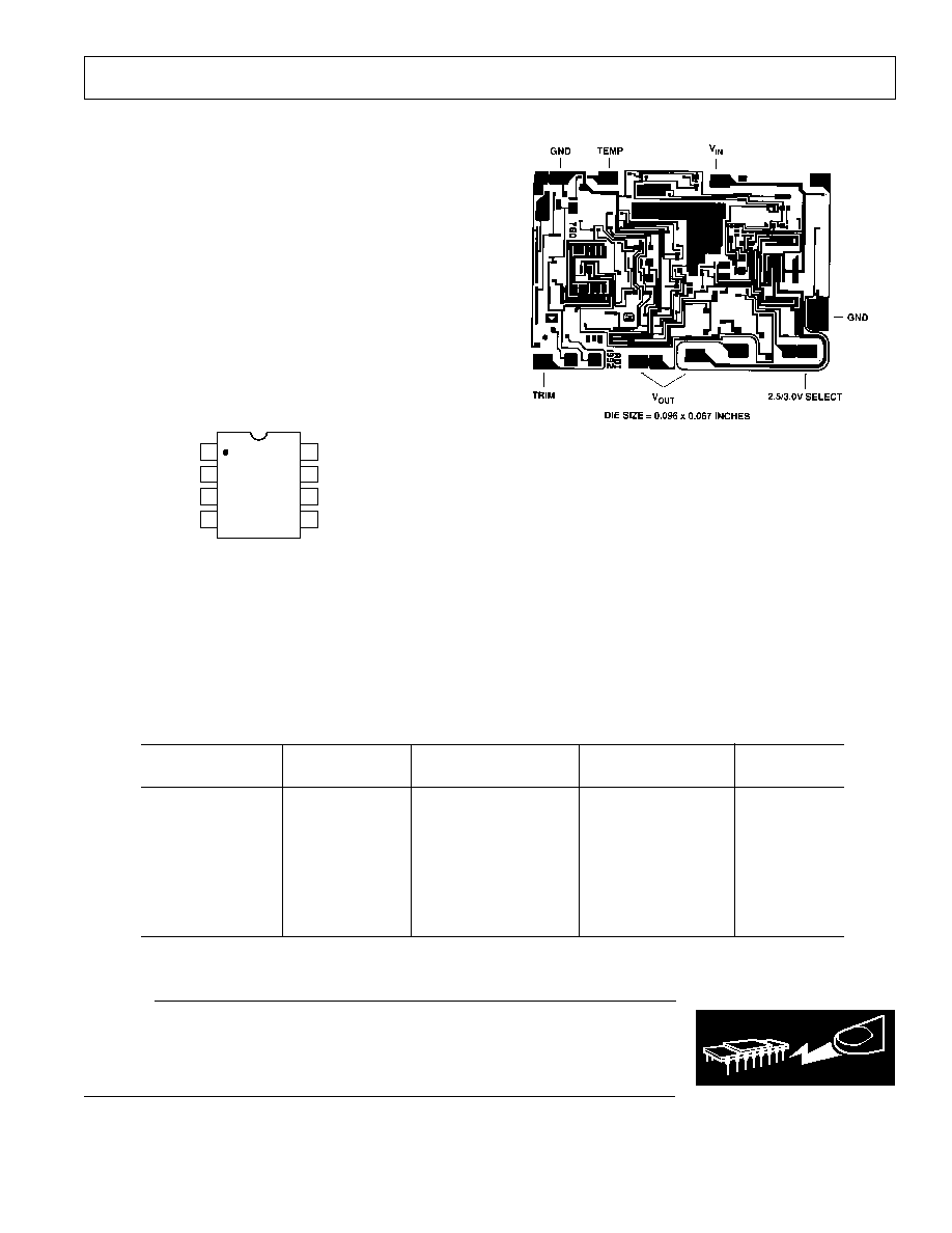
PIN CONFIGURATION
8-Lead Plastic DIP, SOIC and Cerdip Packages
1
2
3
4
8
7
6
5
TOP VIEW
(Not to Scale)
AD780
2.5/3.0V SELECT
(NC OR GND)
NC
V
OUT
TRIM
NC
+V
IN
TEMP
GND
NC = NO CONNECT
DIE LAYOUT
NOTES
Both V
OUT
pads should be connected to the output
Die Thickness: The standard thickness of Analog Devices Bipolar dice is
24 mils
±2 mils.
Die Dimensions: The dimensions given have a tolerance of
± 2 mils.
Backing: The standard backside surface is silicon (not plated). Analog Devices
does not recommend gold-backed dice for most applications.
Edges: A diamond saw is used to separate wafers into dice thus providing per-
pendicular edges half-way through the die.
In contrast to scribed dice, this technique provides a more uniform die shape
and size. The perpendicular edges facilitate handling (such as tweezer pick-up)
while the uniform shape and size simplifies substrate design and die attach.
Top Surface: The standard top surface of the die is covered by a layer of
glassivation. All areas are covered except bonding pads and scribe lines.
Surface Metalization: The metalization to Analog Devices bipolar dice is alu-
minum. Minimum thickness is 10,000Å.
Bonding Pads: All bonding pads have a minimum size of 4.0 mils by 6.0 mils.
The passivation windows have a 3.6 mils by 5.6 mils minimum size.
CAUTION
ESD (electrostatic discharge) sensitive device. Electrostatic charges as high as 4000 V readily
accumulate on the human body and test equipment and can discharge without detection.
Although the AD780 features proprietary ESD protection circuitry, permanent damage may
occur on devices subjected to high-energy electrostatic discharges. Therefore, proper ESD
precautions are recommended to avoid performance degradation or loss of functionality.
WARNING!
ESD SENSITIVE DEVICE
AD780
REV. B
4
THEORY OF OPERATION
Bandgap references are the high performance solution for low
supply voltage and low power voltage reference applications. In
this technique a voltage with a positive temperature coefficient is
combined with the negative coefficient of a transistor's Vbe to
produce a constant bandgap voltage.
In the AD780, the bandgap cell contains two npn transistors
(Q6 and Q7) which differ in emitter area by 12 . The differ-
ence in their Vbe's produces a PTAT current in R5. This in
turn produces a PTAT voltage across R4, which when com-
bined with the Vbe of Q7, produces a voltage Vbg that does not
vary with temperature. Precision laser trimming of the resistors
and other patented circuit techniques are used to further enhance
the drift performance.
NC
TEMP
+V
IN
V
OUT
TRIM
GND
O/P SELECT
2.5V - NC
3.0V - GND
Q6
Q7
R10
R11
R5
R4
R14
R15
R16
R13
NC = NO CONNECT
NC
AD780
Figure 1. Schematic Diagram
The output voltage of the AD780 is determined by the configu-
ration of resistors R13, R14 and R15 in the amplifier's feedback
loop. This sets the output to either 2.5 V or 3.0 V depending on
whether R15 (Pin 8) is grounded or not connected.
A unique feature of the AD780 is the low headroom design of
the high gain amplifier which produces a precision 3 V output
from an input voltage as low as 4.5 V (or 2.5 V from a 4.0 V
input). The amplifier design also allows the part to work with
V
IN
= V
OUT
when current is forced into the output terminal.
This allows the AD780 to work as a two terminal shunt regula-
tor providing a 2.5 V or 3.0 V reference voltage output with-
out external components.
The PTAT voltage is also used to provide the user with a ther-
mometer output voltage (at Pin 3) which increases at a rate of
approximately 2 mV/
°C.
The AD780's NC Pin 7 is a 20 k
resistor to V+ which is used
solely for production test purposes. Users who are currently us-
ing the LT1019 self-heater pin (Pin 7) must take into account
the different load on the heater supply.
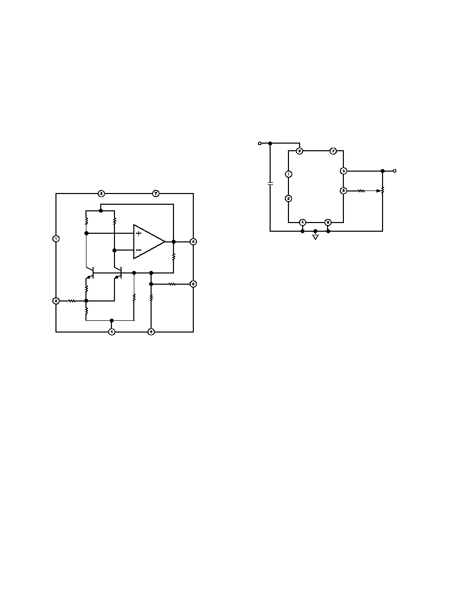
APPLYING THE AD780
The AD780 can be used without any external components to
achieve specified performance. If power is supplied to Pin 2 and
Pin 4 is grounded, Pin 6 provides a 2.5 V or 3.0 V output de-
pending on whether Pin 8 is left unconnected or grounded.
A bypass capacitor of 1
µF (V
IN
to GND) should be used if the
load capacitance in the application is expected to be greater
than 1 nF. The AD780 in 2.5 V mode typically draws 700
µA of
Iq at 5 V. This increases by ~2
µA/V up to 36 V.
NC
TEMP
+V
IN
V
OUT
TRIM
GND
O/P SELECT
2.5V NC
3.0V GND
NC
R
NULL
R POT.
1 F
AD780
NC = NO CONNECT
Figure 2. Optional Fine Trim Circuit
Initial error can be nulled using a single 25 k
potentiometer
connected between V
OUT
, Trim and GND. This is a coarse trim
with an adjustment range of
±4% and is only included here for
compatibility purposes with other references. A fine trim can be
implemented by inserting a large value resistor (e.g. 15 M
) in
series with the wiper of the potentiometer. See Figure 2 above.
The trim range, expressed as a fraction of the output, is simply
greater than or equal to 2.1 k
/R
NULL
for either the 2.5 V or
3.0 V mode.
The external null resistor affects the overall temperature coeffi-
cient by a factor equal to the percentage of V
OUT
nulled.
For example a 1 mV (.03%) shift in the output caused by the
trim circuit, with a 100 ppm/
°C null resistor will add less than
0.06 ppm/
°C to the output drift (0.03% 200 ppm/°C, since
the resistors internal to the AD780 also have temperature coeffi-
cients of less than 100 ppm/
°C).
AD780
REV. B
5
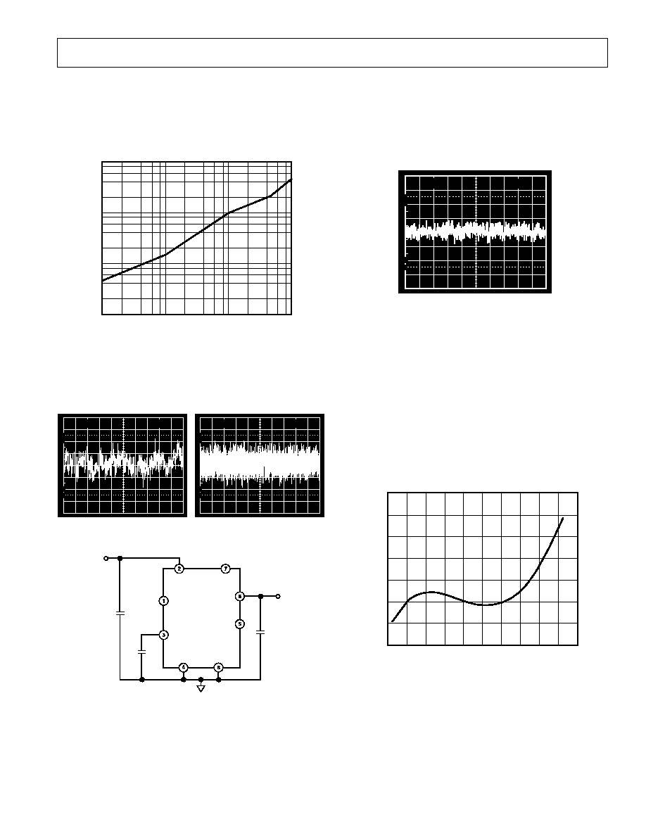
NOISE PERFORMANCE
The impressive noise performance of the AD780 can be further
improved if desired by the addition of two capacitors: a load ca-
pacitor C1 between the output and ground, and a compensation
capacitor C2 between the TEMP pin and ground. Suitable val-
ues are shown in Figure 3.
100
1
0.1
0.1
1
100
10
10
LOAD CAPACITOR, C1 F
COMPENSATION CAP, C2
nF
Figure 3. Compensation and Load Capacitor Combinations
C1 and C2 also improve the settling performance of the AD780
when subjected to load transients. The improvement in noise
performance is shown in Figures 4, 5 and 6 following.
10
90
100
0%
100 V
1s
0.1 TO
10Hz
AMPLIFIER GAIN = 100
10
90
100
0%
20 V
10ms
10Hz
TO 10kHz
NO AMPLIFIER
Figure 4. Stand-Alone Noise Performance
NC
TEMP
+V
IN
V
OUT
TRIM
GND
O/P SELECT
2.5V NC
3.0V GND
NC
AD780
NC = NO CONNECT
C2
1 F
C1
Figure 5. Noise Reduction Circuit
NOISE COMPARISON
The wideband noise performance of the AD780 can also be ex-
pressed in ppm. The typical performance with C1, C2 is
0.6 ppm and without external capacitors is 1.2 ppm.
This performance is respectively 7 and 3 lower than the
specified performance of the LT1019.
10
90
100
0%
20 V
10ms
10Hz TO 10kHz
NO AMPLIFIER
Figure 6. Reduced Noise Performance with C1 = 100
µF,
C2 = 100 nF
TEMPERATURE PERFORMANCE
The AD780 provides superior performance over temperature by
means of a combination of patented circuit design techniques,
precision thin film resistors and drift trimming. Temperature
performance is specified in terms of ppm/
°C, but because of
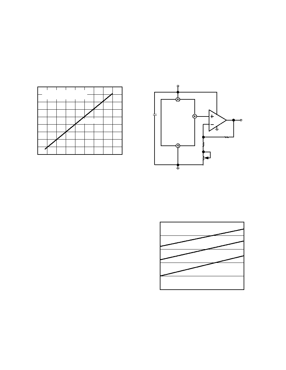
nonlinearity in the temperature characteristic, the Box-Test
method is used to test and specify the part. The nonlinearity
takes the form of the characteristic S-shaped curve shown in
Figure 7. The Box-Test method forms a rectangular box around
this curve, enclosing the maximum and minimum output volt-
ages over the specified temperature range. The specified drift is
equal to the slope of the diagonal of this box.
2.0
0.8
140
0.4
0.4
40
0
60
1.6
0.8
1.2
120
100
80
60
40
20
0
20
TEMPERATURE C
ERROR
mV
Figure 7. Typical AD780BN Temperature Drift
AD780
REV. B
6
TEMPERATURE OUTPUT PIN
The AD780 provides a "TEMP" output (Pin 3) that varies
linearly with temperature. This output can be used to monitor
changes in system ambient temperature and to initiate calibration
of the system if desired. The voltage V
TEMP
is 560 mV at 25
°C,
and the temperature coefficient is approximately 2 mV/
°C.
Figure 8 shows the typical V
TEMP
characteristic curve over tem-
perature taken at the output of the op amp with a noninverting
gain of five.
4.25
2.00
150
2.50
2.25
50
75
2.75
3.00
3.25
3.50
3.75
4.00
125
100
75
50
25
0
25
TEMPERATURE C
VOLTAGE
V
OUT
CIRCUIT CALIBRATED AT 25 C
REFER TO FIGURE 9
10mV PER C
Figure 8. Temperature Pin Transfer Characteristic
Since the TEMP voltage is acquired from the bandgap core cir-
cuit, current pulled from this pin will have a significant effect on
V
OUT
. Care must be taken to buffer the TEMP output with a
suitable op amp, e.g., an OP07, AD820 or AD711 (all of which
would result in less than a 100
µV change in V
OUT
). The rela-
tionship between I
TEMP
and V
OUT
is as follows:
V
OUT
= 5.8 mV/
µA × I
TEMP
(2.5 V range)
or
V
OUT
= 6.9 mV/
µA × I
TEMP
(3.0 V range)
Notice how sensitive the current dependent factor on V
OUT
is. A
large amount of current, even in tens of microamp, drawn from
TEMP pin can cause V
OUT
and TEMP Output to fail.
The choice of C1 and C2 was dictated primarily by the need for a
relatively flat response that rolled off early in the high frequency
noise at the output. But there is considerable margin in the
choice of these capacitors. For example, the user can actually
put a huge C2 on the TEMP pin with none on the output pin.
However, one must either put very little or a lot of capacitance at
the TEMP pin. Intermediate values of capacitance can sometimes
cause oscillation. In any case, the user should follow the recom-
mendation in Figure 3.
TEMPERATURE TRANSDUCER CIRCUIT
The circuit shown in Figure 9 is a temperature transducer which
a amplifies the TEMP output voltage by a gain of a little over 5
to provide a wider full scale output range. The trimpot can be
used to adjust the output so it varies exactly by 10 mV/
°C.
To minimize resistance changes with temperature, resistors with
low temperature coefficients, such as metal film resistors should
be used.
+5V
V
IN
TEMP
GND
AD820
6.04k (1%)
1.27k
(1%)
200
R
F
R
B
R
BP
10mV/ C
1 F
AD780
Figure 9. Differential Temperature Transducer
SUPPLY CURRENT OVER TEMPERATURE
The AD780's quiescent current will vary slightly over tempera-
ture and input supply range. The test limit is 1 mA over the in-
dustrial and 1.3 mA over the military temperature range.
Typical performance with input voltage and temperature varia-
tion is shown in Figure 10 following.
0.85
0.60
36
0.75
0.65
0.70
4
0.80
INPUT VOLTAGE Volts
QUIESCENT CURRENT
mA
55 C
125 C
25 C
Figure 10. Typical Supply Current over Temperature
AD780
REV. B
7
TURN-ON TIME
The time required for the output voltage to reach its final value
within a specified error band is defined as the turn-on settling
time. The two major factors that affect this are the active circuit
settling time and the time for the thermal gradients on the chip
to stabilize. Typical settling performance is shown in Figure 11
following. The AD780 settles to within 0.1% of its final value
within 10
µs.
2.499V
2.498V
2.500V
0V
5V
10 s/DIV
V
IN
V
OUT
Figure 11. Turn-On Settling Time Performance
DYNAMIC PERFORMANCE
The output stage of the AD780 has been designed to provide
superior static and dynamic load regulation.
Figure 12 shows the performance of the AD780 while driving a
0 mA to 10 mA load.
+V
IN
V
OUT
AD780
V
L
0V
V
OUT
249
1 F
Figure 12a. Transient Resistive Load Test Circuit
OUTPUT CHANGE
50mV/DIV
10mA
0mA
10 s/DIV
I
LOAD
V
OUT
(C
L
= 0pF)
Figure 12b. Settling Under Transient Resistive Load
The dynamic load may be resistive and capacitive. For example
the load may be connected via a long capacitive cable. Figure 13
following shows the performance of the AD780 driving a
1000 pF, 0 mA to 10 mA load.
+V
IN
V
OUT
AD780
V
L
0V
V
OUT
249
1 F
C
L
1000pF
Figure 13a. Capacitive Load Transient Response
Test Circuit
OUTPUT CHANGE
50mV/DIV
10 s/DIV
0mA
10mA
I
LOAD
V
OUT
(C
L
= 1000pF)
Figure 13b. Settling Under Dynamic Capacitive Load
AD780
REV. B
8
LINE REGULATION
Line regulation is a measure of the change in output voltage due
to a specified change in input voltage. It is intended to simulate
worst case unregulated supply conditions and is measured in
µV/V. Figure 14 shows typical performance with 4.0 V < V
IN
<
15.0 V.
200
200
4
15
100
100
10
0
INPUT VOLTAGE Volts
OUTPUT CHANGE
V
T = 25 C
Figure 14. Output Voltage Change vs. Input Voltage
PRECISION REFERENCE FOR HIGH RESOLUTION
+5 V DATA CONVERTERS
The AD780 is ideally suited to be the reference for most +5 V
high resolution ADCs. The AD780 is stable under any capaci-
tive load, it has superior dynamic load performance, and the
3.0 V output provides the converter with maximum dynamic
range without requiring an additional and expensive buffer am-
plifier. One of the many ADCs that the AD780 is suited for is
the AD7884, a 16-bit, high speed sampling ADC. (See Figure
15.) This part previously needed a precision 5.0 V reference, re-
sistor divider and buffer amplifier to do this function.
+5V
V
IN
V
OUT
GND
AD780
1 F
V
REF
+F
V
REF
+S
AD7884
2.5/3.0V
SELECT
Figure 15. Precision 3.0 V Reference for the AD7884
16-Bit, High Speed ADC
The AD780 is also ideal for use with higher resolution convert-
ers such as the AD7710/AD7711/AD7712. (See Figure 16.)
While these parts are specified with a 2.5 V internal reference,
the AD780 in 3 V mode can be used to improve the absolute ac-
curacy, temperature stability and dynamic range. It is shown fol-
lowing with the two optional noise reduction capacitors.
+5V
V
IN
V
OUT
GND
AD780
1 F
REFIN+
REFIN
AD7710
2.5/3.0V
SELECT
100 F
100nF
Figure 16. Precision 2.5 V or 3.0 V Reference for the
AD7710 High Resolution, Sigma-Delta ADC
+4.5 V REFERENCE FROM +5 V SUPPLY
Some +5 V high resolution ADCs can accommodate reference
voltages up to +4.5 V. The AD780 can be used to provide a
precision +4.5 V reference voltage from a +5 V supply using the
circuit shown following in Figure 17. This circuit will provide a
regulated +4.5 V output from a supply voltage as low as +4.7 V.
The high quality tantalum 10
µF capacitor in parallel with the
ceramic 0.1
µF capacitor and the 3.9 resistor ensure a low
output impedance up to around 50 MHz.
AD780
2N2907
10 F
3.9
4k
0.01%
5k
0.01%
0.1 F
0.1 F
1k
V
SUPPLY
V
OUT
OP90
2.5k
0.1 F
Figure 17. +4.5 V Reference from a Single +5 V Supply
AD780
REV. B
9
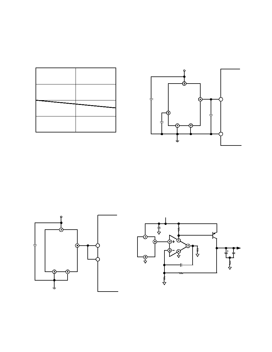
NEGATIVE (2.5 V OR 3.0 V) REFERENCE
The AD780 can produce a negative output voltage in shunt
mode, simply by connecting the input and output to ground
connecting the AD780's GND pin to a negative supply via a
bias resistor as shown in Figure 18.
NC
TEMP
+V
IN
V
OUT
TRIM
GND
O/P SELECT
2.5V NC
3.0V GND
NC
1 F
AD780
V
2.5 V
OUT
NOTE:
I
L
= LOAD CURRENT
I
S
MIN = MINIMUM SHUNT CURRENT
NC = NO CONNECT
V
OUT
(V)
I
L
+ I
S
MIN
R =
Figure 18. Negative (2.5 V) Shunt Mode Reference
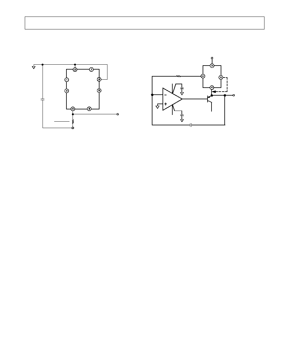
A precise 2.5 V (or 3.0 V) reference capable of supplying up
to 100 mA to a load can be implemented with the AD780 in se-
ries mode using the bootstrap circuit following.
AD780
2N3906
+5V
+5V
OP07
CONNECT IF
3V OUTPUT
DESIRED
5V
2.5V (I
L
100mA)
5V
OUT
1k
1000pF
V
IN
Figure 19. 2.5 V High Load Current Reference
AD780
REV. B
10
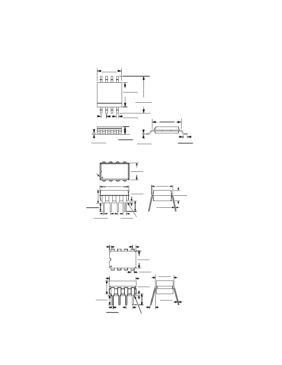
OUTLINE DIMENSIONS
Dimensions shown in inches and (mm).
SOIC (R) Package
1
4
5
8
0.050
(1.27)
TYP
0.188 (4.75)
0.198 (5.00)
0.150 (3.80)
0.158 (4.00)
0.228 (5.80)
0.244 (6.200)
0.014 (0.36)
0.018 (0.46)
0.181 (4.60)
0.205 (5.20)
0.053 (1.35)
0.069 (1.75)
0.020 (0.50)
0.045 (1.15)
0.007 (0.18)
0.015 (0.38)
0.004 (0.10)
0.010 (0.25)
Plastic Mini-DIP (N) Package
PIN 1
0.280 (7.11)
0.240 (6.10)
4
5
8
1
SEATING
PLANE
0.060 (1.52)
0.015 (0.38)
0.130
(3.30)
MIN
0.210
(5.33)
MAX
0.160 (4.06)
0.115 (2.93)
0.430 (10.92)
0.348 (8.84)
0.022 (0.558)
0.014 (0.356)
0.070 (1.77)
0.045 (1.15)
0.100
(2.54)
BSC
0.325 (8.25)
0.300 (7.62)
0.015 (0.381)
0.008 (0.204)
0.195 (4.95)
0.115 (2.93)
Cerdip (Q) Package
0.005 (0.13) MIN
0.055 (1.4) MAX
0.405 (10.29) MAX
0.150
(3.81)
MIN
0.200
(5.08)
MAX
0.070 (1.78)
0.030 (0.76)
0.200 (5.08)
0.125 (3.18)
0.023 (0.58)
0.014 (0.36)
0.320 (8.13)
0.290 (7.37)
0
°-15°
0.015 (0.38)
0.008 (0.20)
0.100 (2.54)
BSC
SEATING PLANE
0.060 (1.52)
0.015 (0.38)
4
1
5
8
0.310 (7.87)
0.220 (5.59)
C175806/00 (rev. B) 00841
PRINTED IN U.S.A.