 | ÐлекÑÑоннÑй компоненÑ: AD7401 | СкаÑаÑÑ:  PDF PDF  ZIP ZIP |
Äîêóìåíòàöèÿ è îïèñàíèÿ www.docs.chipfind.ru
Isolated Sigma-Delta Modulator
Preliminary Technical Data
AD7400/AD7401
FEATURES
Up to 20 MHz Data Rate (AD7401)
10 MHz Data Rate (AD7400)
2
nd
Order Modulator
±4 LSB INL @16 Bits
Onboard Digital Isolator
Onboard Reference
Low Power Operation:
15 mA @ 5 V
-40 C to +105 C Operating Range
16-ld SOIC Package
Safety and Regulatory Approvals
UL
Recognition
3750 V
RMS
for 1 minute per UL 1577
CSA Component Acceptance Notice ~5A
VDE Certificate of Conformity
DIN EN 60747-5-2 (VDE 0884 Part 2):2003-01
DIN EN 60950 (VDE 0805): 2001-12; EN 60950:2000
V
IORM
= 840V
PEAK
APPLICATIONS
AC Motor Control
Data Acquisition Systems
A/D + Opto-Isolator Replacement
GENERAL DESCRIPTION
The AD7400/AD7401 are 2nd order sigma-delta modulators
that convert an analog input signal into a high speed 1-bit data
stream with onboard digital isolation based on Analog Devices'
iCoupler® technology. The AD7400/AD7401 operate from a 5 V
power supply and accept a differential input signal of ±200 mV.
The analog input is continuously sampled by the analog
modulator, eliminating the need for external sample and hold
circuitry. The input information is contained in the output
stream as a density of ones with data rates up to 20MHz. The
original information can be reconstructed with an appropriate
digital filter. The serial I/O may use a 5V or 3V supply (V
DD2
).
The serial interface is digitally isolated. High-speed CMOS,
FUNCTIONAL BLOCK DIAGRAM
UPDATE
ENCODE DECODE
WATCHDOG
T/H
VDD1
- ADC
MCLKOUT*
CONTROL LOGIC
MDAT
GND1
VDD2
GND2
VIN+
VIN-
REF
BUF
UPDATE
ENCODE DECODE
WATCHDOG
*MCLKIN pin on AD7401
Rev. PrH
Information furnished by Analog Devices is believed to be accurate and reliable.
However, no responsibility is assumed by Analog Devices for its use, nor for any
infringements of patents or other rights of third parties that may result from its use.
Specifications subject to change without notice. No license is granted by implication
or otherwise under any patent or patent rights of Analog Devices. Trademarks and
registered trademarks are the property of their respective companies.
One Technology Way, P.O. Box 9106, Norwood, MA 02062-9106, U.S.A.
Tel: 781.329.4700
www.analog.com
Fax: 781.326.8703
© 2004 Analog Devices, Inc. All rights reserved.

AD7400/AD7401
Preliminary Technical Data
combined with monolithic air core transformer technology, means the onboard isolation provides outstanding performance
characteristics superior to alternatives such as optocoupler devices. The parts provide an on-chip 2.5V reference. The AD7400/AD7401
are offered in a 16-lead SOIC package and have an operating temperature range of -40°C to +105°C.
TABLE OF CONTENTS
AD7400--Specifications.................................................................. 3
AD7401--Specifications.................................................................. 4
TIMING SPECIFICATIONS
1
..................................................... 5
Absolute Maximum Ratings
1,3
......................................................... 6
Pin Functional Descriptions ........................................................8
Theory of Operation.....................................................................9
Outline Dimensions ....................................................................... 10
REVISION HISTORY
Revision PrH: Preliminary Version
Rev. PrH | Page 2 of 10
Preliminary Technical Data
AD7400/AD7401
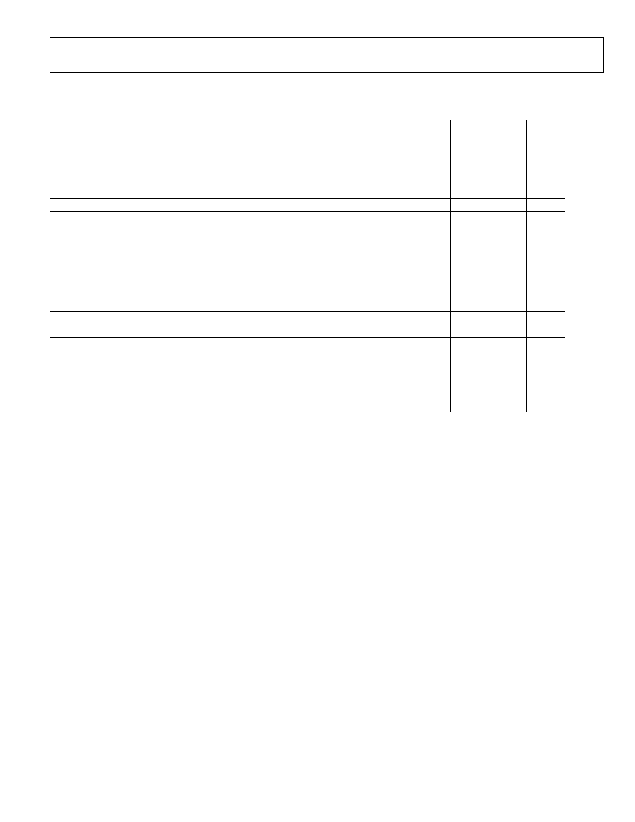
AD7400--SPECIFICATIONS
1
Table 1. (V
DD1
= V
DD2
= 4.5V to 5.5V, , V
IN
+ = -200mV to +200mV and V
IN
- = 0V; T
A
= T
MIN
to T
MAX
, f
MCLK
= 10MHz unless
otherwise noted.)
Parameter B
Version
1,5
Units Test
Conditions/Comments
STATIC PERFORMANCE
When Tested with Sinc
3
Filter
4
Resolution
16
Bits min
Filter output trunctaed to 16 Bits
Integral Nonlinearity
2
±4 LSB
max
Differential Nonlinearity
2
±0.9
LSB max
Guaranteed No Missed Codes to 15 bits
Offset Error
2
±0.5
mV max
Bipolar Input Range
Offset Drift vs. Temperature
2
5
2
µV/ C max
µV/ C typ
Offset Drift vs. V
DD1
2
0.05 mV/V
typ
Absolute Reference Voltage Tolerance
±1
%min/max
Reference Voltage Matching
±TBD
%min/max
V
REF
Drift vs. Temperature
2
60
ppm/ C typ
V
REF
Drift vs. V
DD1
2
0.2
%
typ
ANALOG INPUT
Input Voltage Ranges
6
±200 mV
min/max
DC Leakage Current
±1
µA max
DYNAMIC SPECIFICATIONS
When Tested with Sinc
3
Filter
4
Signal to Noise + Distortion Ratio (SINAD)
2
70
76
dBmin
dB typ
V
IN
+ = 35Hz, 400mV
pk-pk
sine wave
Total Harmonic Distortion (THD)
2
-80 dB
typ
Peak Harmonic or Spurious Noise (SFDR)
2
-70 dB
typ
Effective number of bits
12
Bits
Isolation Transient Immunity
15
20
kV/µs min
kV/µs typ
Signal Delay
20
24
µs typ
µs max
Delay through filter varies with actual value of on-
board clock. Decimation by 2.
LOGIC
INPUTS
Input High Voltage, V
INH
2
V
min
Input Low Voltage, V
INL
0.8
V
max
Input Current, I
IN
±1
µA
max
Input Capacitance, C
IN
3
10 pF
max
LOGIC
OUTPUTS
Output High Voltage, V
OH
V
DD2
0.1
V min
I
O
= -20 µA
Output Low Voltage, V
OL
0.4
V
max
I
O
= 20 µA
POWER
REQUIREMENTS
V
DD1
+4.5/+5.5
Vmin/Vmax
V
DD2
+4.5/+5.5
Vmin/Vmax
+2.7/+3.3
Vmin/Vmax
I
DD1
7
18.1
mA
max
I
DD2
7
1.96 mA
max
V
DD1
= 5V, Digital I/Ps = 0 V or V
DD1
NOTES
1
Temperature ranges as follows: -40 C to +105 C
2
See Terminology section.
3
Sample tested @ 25 C to ensure compliance.
4
Filter as defined by Verilog Code.
5
All voltages are relative to their respective ground.
6
Beyond the full-scale input range the output is either all zeroes or all ones.
Specifications subject to change without notice.
Rev. PrH | Page 3 of 10

AD7400/AD7401
Preliminary Technical Data
AD7401--SPECIFICATIONS
3
Table 2. (V
DD1
= V
DD2
= 4.5V to 5.5V, , V
IN
+ = -200mV to +200mV and V
IN
- = 0V; T
A
= T
MIN
to T
MAX
, f
MCLK
= 20MHz unless
otherwise noted.)
Parameter B
Version
1,5
Units Test
Conditions/Comments
STATIC PERFORMANCE
When Tested with Sinc
3
Filter
4
Resolution
16
Bits min
Filter output trunctaed to 16 Bits
Integral Nonlinearity
2
±4 LSB
max
Differential Nonlinearity
2
±0.9
LSB max
Guaranteed No Missed Codes to 15 bits
Offset Error
2
±0.5
mV max
Bipolar Input Range
Offset Drift vs. Temperature
2
5
2
µV/ C max
µV/ C typ
Offset Drift vs. V
DD1
2
0.05 mV/V
typ
Absolute Reference Voltage Tolerance
±1
%min/max
Reference Voltage Matching
±TBD
%min/max
V
REF
Drift vs. Temperature
2
60
ppm/ C typ
V
REF
Drift vs. V
DD1
2
0.2
%
typ
ANALOG INPUT
Input Voltage Ranges
6
±200 mV
min/max
DC Leakage Current
±1
µA max
DYNAMIC SPECIFICATIONS
When Tested with Sinc
3
Filter
4
Signal to Noise + Distortion Ratio (SINAD)
4
70
76
dBmin
dB typ
V
IN
+ = 35Hz, 400mV
pk-pk
sine wave
Total Harmonic Distortion (THD)
2
-80 dB
typ
Peak Harmonic or Spurious Noise (SFDR)
2
-70 dB
typ
Effective number of bits
12
Bits
Isolation Transient Immunity
15
20
kV/µs min
kV/µs typ
Signal Delay
10
12
µs typ
µs max
Delay through filter varies with actual value of on-
board clock. Decimation by 2.
LOGIC
INPUTS
Input High Voltage, V
INH
2
V
min
Input Low Voltage, V
INL
0.8
V
max
Input Current, I
IN
±1
µA
max
Input Capacitance, C
IN
3
10 pF
max
LOGIC
OUTPUTS
Output High Voltage, V
OH
V
DD2
0.1
V min
I
O
= -20 µA
Output Low Voltage, V
OL
0.4
V
max
I
O
= 20 µA
POWER
REQUIREMENTS
V
DD1
+4.5/+5.5
Vmin/Vmax
V
DD2
+4.5/+5.5
Vmin/Vmax
+2.7/+3.3
Vmin/Vmax
I
DD1
7
21.2
mA
max
I
DD2
7
3.92 mA
max
V
DD1
= 5V, Digital I/Ps = 0 V or V
DD1
NOTES
3
Temperature ranges as follows: -40 C to +105 C
4
See Terminology section.
3
Sample tested @ 25 C to ensure compliance.
4
Filter as defined by Verilog Code.
5
All voltages are relative to their respective ground.
6
Beyond the full-scale input range the output is either all zeroes or all ones.
Specifications subject to change without notice.
Rev. PrH | Page 4 of 10
Preliminary Technical Data
AD7400/AD7401
TIMING SPECIFICATIONS
1
Table 3. AD7400/AD7401 Timing Specifications
(V
DD1
= V
DD2
= 4.5V to 5.5V,
T
A
= T
MAX
to T
MIN
unless otherwise noted.)
Parameter
Limit at T
MIN
, T
MAX
Unit Description
F
MCLKOUT
10 MHz
typ
AD7400
8.2/13.2
MHz
min/max
T
MCLKIN
2
1 MHz
min
AD7401
20
MHz
max
t
1
3
30
ns max
Data Access Time after MCLK Rising Edge
t
2
3
15
ns min
Data Hold Time after MCLK Rising Edge
t
3
0.4 x t
MCLKIN
ns max
Master Clock Low Time
t
4
0.4 x t
MCLKIN
ns max
Master Clock High Time
NOTES
1
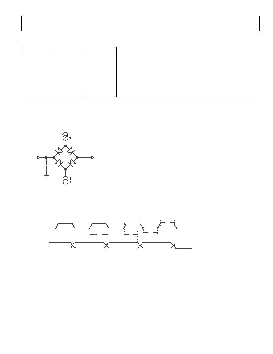
Sample tested @ 25 C to ensure compliance. All input signals are specified with tr = tf = 5ns (10% to 90% of V
DD1
) and timed form a voltage level of 1.6 Volts. See Figure
1.
2
Mark Space ratio for the MCLKIN input is 40/60 to 60/40.
3
Measured with the load circuit of Figure 1 and defined as the time required for the output to cross 0.8V or 2.0V.
+1.6V
IOL
200µA
200µA
IOH
TO
OUTPUT
PIN
CL
50pF
Figure 1. Load Circuit for Digital Output Timing Specifications
MCLKIN /
MCLKOUT
MDAT
t
1
t
2
t
3
t
4
Figure 2. Data Timing
Rev. PrH | Page 5 of 10
AD7400/AD7401
Preliminary Technical Data
ABSOLUTE MAXIMUM RATINGS
1,3
Table 4. AD7400/AD7401 Absolute Maximum Ratings
(T
A
= +25°C unless otherwise noted)
V
DD1
to GND
1
-0.3 V to +6.5V
V
DD2
to GND
2
-0.3 V to +6.5 V
Analog Input Voltage to GND
1
-0.3 V to V
DD1
+0.3V
Digital Input Voltage to GND
2
-0.3 V to V
DD2
+0.5 V
Output Voltage to GND
2
-0.3 V to V
DD2
+0.3V
Input Current to Any Pin Except Supplies
2
±10mA
Operating Temperature Range
-40°C to +105°C
Storage Temperature Range
-65°C to +150°C
Junction Temperature
+150°C
SOIC Package
JA
Thermal Impedance
89.2 °C/W
JC
Thermal Impedance
55.6 °C/W
Resistance (Input-Output), R
I-O
10
12
Capacitance (Input-Output), C
I-O
1pF
Lead Temperature, Soldering
Vapor Phase (60 sec)
+215°C
Infared (15 sec)
+220°C
ESD TBD
NOTES
1
Stresses above those listed under Absolute Maximum Ratings may cause
permanent damage to the device. This is a stress rating only and functional
operation of the device at these or any other conditions above those
indicated in the operational section of this specification is not implied.
Exposure to absolute maximum rating conditions for extended periods may
affect device reliability.
2
Transient currents of up to 100mA will not cause SCR latch up.
3
All voltages are relative to their respective ground.
REGULATORY INFORMATION
(PENDING)
Table 5. Insulation and Safety Related Specifications
Parameter Symbol
Value
Units
Conditions
Input-Output Withstand Momentary
Withstand Voltage
1
V
ISO
3750 min.
V
Note 1
Minimum External Air Gap
(Clearance)
L(I01) 8.4
min mm
Measured from input terminals to output terminals, shortest
distance through air.
Minimum External Tracking
(Creepage)
L(I02) 8.1
min mm
Measured from input terminals to output terminals, shortest
distance path along body.
Minimum Internal Gap (Internal
Clearance)
0.025 min
mm
Insulation distance through insulation.
Tracking Resistance (Comparative
Tracking Index)
CTI
>175
V
DIN IEC 112/VDE 0303 Part 1
Isolation Group
IIIa
Material Group (DIN VDE 0110,1/89,Table 1)
UL
1
CSA
VDE
2
Recognized under 1577
component recognition program
1
Double insulation, 3750 V rms
isolation voltage
Approved under CSA Component
Acceptance Notice #5A
Reinforced insulation per
CSA 60950-1-03 and IEC 60950-1,
630 V rms maximum working voltage
Certified according to DIN EN 60747-5-2
(VDE 0884 Part 2):2003-01
2
Basic insulation, 891 V peak
Complies with DIN EN 60747-5-2 (VDE 0884 Part 2):2003-01,
DIN EN 60950 (VDE 0805):2001-12; EN 60950:2000
Reinforced insulation, 891 V peak
NOTES
1
In accordance with UL1577, each AD7400/AD7401 is proof tested by applying an insulation test voltage 4500 V rms for 1 second (current leakage detection limit =
5 µA).
2
In accordance with DIN EN 60747-5-2, each AD7400/AD7401 is proof tested by applying an insulation test voltage 1670 V peak for 1 second (partial discharge
detection limit = 5 pC).
Rev. PrH | Page 6 of 10
Preliminary Technical Data
AD7400/AD7401
DIN EN 60747-5-2 (VDE 0884 PART 2) INSULATION CHARACTERISTICS (PENDING)
Table 6.
Description
Symbol Characteristic Unit
Installation classification per DIN VDE 0110
For Rated Mains Voltage 300 V rms
For Rated Mains Voltage 600 V rms
IIV
IIII
Climatic Classification
40/105/21
Pollution Degree (DIN VDE 0110, Table 1)
2
Maximum Working Insulation Voltage
V
IORM
891
Vpeak
Input to Output Test Voltage, Method b1
V
IORM
× 1.875 = V
PR
, 100% Production Test,
t
m
= 1 sec, Partial Discharge < 5 pC
V
PR
1670
V peak
Input to Output Test Voltage, Method a
After Environmental Tests Subgroup 1)
V
IORM
× 1.6 = V
PR
, t
m
= 60 sec, Partial Discharge < 5p C
After Input and/or Safety Test Subgroup 2/3)
V
IORM
× 1.2 = V
PR
, t
m
= 60 sec, Partial Discharge < 5p C
V
PR
1426
1069
Vpeak
Vpeak
Highest Allowable Overvoltage
(Transient Overvoltage, t
TR
= 10 sec)
V
TR
6000
V
peak
Safety-Limiting Values (Maximum value allowed in the event of a failure, also see Thermal
Derating Curve)
Case
Temperature
Side 1 Current
Side 2 Current
T
S
I
S1
I
S2
150
TBD
TBD
°C
mA
mA
Insulation Resistance at T
S
, V
IO
= 500 V
R
S
>10
9
This isolator is suitable for "basic electrical isolation" only within the safety limit data. Maintenance of the safety data shall be ensured by
means of protective circuits.
"*" marking on packages denotes DIN EN 60747-5-2 approval for 891 V peak working voltage.
Rev. PrH | Page 7 of 10
AD7400/AD7401
Preliminary Technical Data
16
15
14
13
12
11
9
TOP VIEW
(Not to Scale)
8
1
2
3
4
7
6
5
AD7400
NC
V
DD1
GND1
10
MDAT
NC
VIN+
VIN-
NC
NC
GND2
GND2
NC
MCLKOUT
NC
V
DD2
V
DD1
16
15
14
13
12
11
9
TOP VIEW
(Not to Scale)
8
1
2
3
4
7
6
5
AD7401
NC
V
DD1
GND1
10
MDAT
NC
VIN+
VIN-
NC
NC
GND2
GND2
NC
MCLKIN
NC
V
DD2
V
DD1
Pin Functional Descriptions
Table 7. AD7400/AD7401 Pin Function Descriptions
Pin
Number
AD7400
Pin
Mnemonic
AD7401 Pin
Mnemonic
Description
1,7 V
DD1
V
DD1
Supply Voltage, 5 V ±10%. This is the supply voltage for the isolated side of the
AD7400/AD7401 and is relative to GND
1
.
2 V
IN
+ V
IN
+
Positive analog Input, range of ±200 mV .
3 V
IN
-
V
IN
-
Negative analog input (normally connected to GND
1
).
18 MCLKIN
Master Clock. Logic Input. An external clock is applied at this pin. A serial clock input from
1MHz to 20MHz may be applied to this pin on the AD7401. The bit stream form the
modultaor is valid on the rising edge of MCLKIN.
18 MCLKOUT
Master Clock. Logic Output, 10MHz typical. The bit stream form the modultaor is valid on the
rising edge of MCLKOUT on the AD7400.
14 V
DD2
V
DD2
Supply Voltage, 5 V ±10% or 3V ±10%. This is the supply voltage for the non-isolated side of
the AD7400/AD7401 and is relative to GND
2
.
8 GND
1
GND
1
Ground. This is the ground reference point for all circuitry on the isolated side of the
AD7400/AD7401.
9,16 GND
2
GND
2
Ground. This is the ground reference point for all circuitry on the non-isolated side of the
AD7400/AD7401.
4-6,10,12,15 NC
NC
No
Connect
Rev. PrH | Page 8 of 10
Preliminary Technical Data
AD7400/AD7401
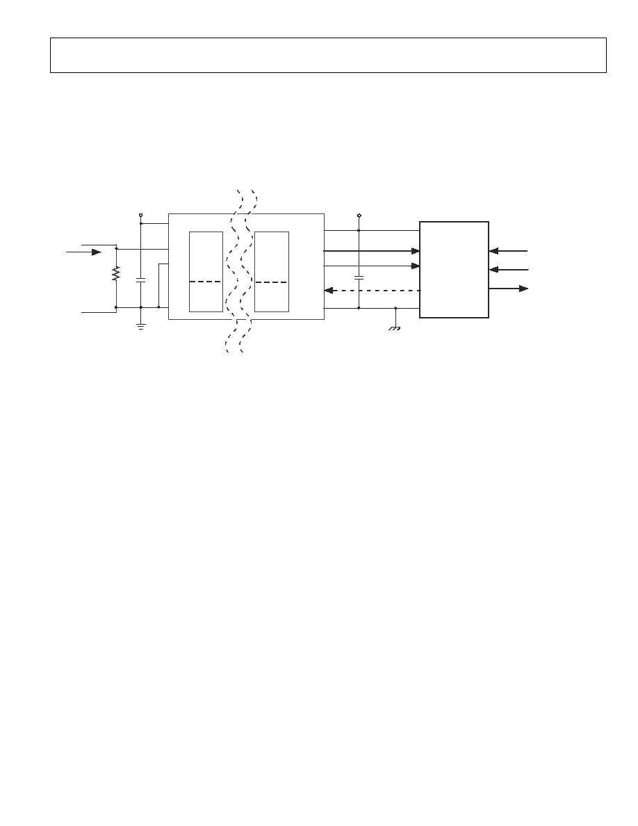
Theory of Operation
CIRCUIT INFORMATION
The AD7400/AD7401 Isolated Sigma-Delta Modulator converts
an analog input signal into a high-speed, (10MHz using on-
board MCLK on AD7400, or up to 20MHz using external
MCLK on AD7401), single-bit data stream; the time average of
the modulator's single-bit data is directly proportional to the
input signal. Figure 4 shows a typical application circuit where
the AD7400/AD7401 is used to provide isolation between the
analog input, a current sensing resistor, and the digital output
which is then processed by a digital filter to provide an N-bit
word.
MCLKIN
V
DD1
GND1
MDAT
VIN+
VIN-
GND2
MCLKOUT
V
DD2
SIGMA-
DELTA
MOD/
ENCODER
DECODER
DECODER
ENCODER
SINC3 FILTER
+
ISOLATED
+5V
R
SHUNT
INPUT
CURRENT
NON-ISOLATED
+5V/+3V
V
DD
GND
MDAT
MCLK
CCLK
(UP TO 20MHz
with AD7401)
SDAT
SCLK
+5
AD7400
Figure 4. Typical Application Circuit
Table 8. Analog Input Range
Analog Input
Voltage Input
Full Scale Range
640 mV
+Full Scale
+320 mV
+ Specified Input range
+200 mV
Zero 0
mV
-Specified Input range
-200 mV
-Full Scale
-320mV
Rev. PrH | Page 9 of 10
AD7400/AD7401
Preliminary Technical Data
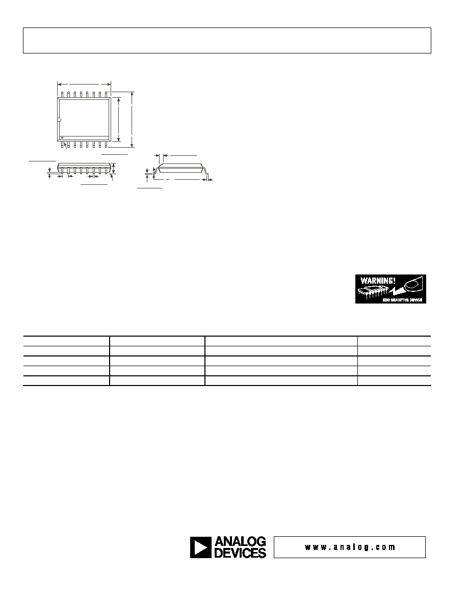
OUTLINE DIMENSIONS
0.2992 (7.60)
0.2913 (7.40)
$
'
&
0.4134 (10.50)
0.3976 (10.10)
0.4193 (10.65)
0.3937 (10.00)
PIN 1
SEATING
PLANE
0.0118 (0.30)
0.0039 (0.10)
0.0201 (0.51)
0.0130 (0.33)
0.1043 (2.65)
0.0925 (2.35)
0.0500
(1.27)
BSC
0.0126 (0.32)
0.0091 (0.23)
0.0500 (1.27)
0.0157 (0.40)
0.0295 (0.75)
0.0098 (0.25)
x 45°
8°
0°
Figure 2. 16-Lead Short Outline Package [SOIC] Wide Body (RW-16)--Dimensions shown in millimeters
ESD CAUTION
ESD (electrostatic discharge) sensitive device. Electrostatic charges as high as 4000 V readily accumulate on the
human body and test equipment and can discharge without detection. Although this product features
proprietary ESD protection circuitry, permanent damage may occur on devices subjected to high energy
electrostatic discharges. Therefore, proper ESD precautions are recommended to avoid performance
degradation or loss of functionality.
Ordering Guide
AD7266 Products
Temperature Package
Package Description
Package Outline
AD7400BRW
40°C to +105°C
Short Outline I.C. Package
RW-16
AD7401BRW
40°C to +105°C
Short Outline I.C. Package
RW-16
© 2004 Analog Devices, Inc. All rights reserved. Trademarks and
registered trademarks are the property of their respective companies.
Printed in the U.S.A.
Rev. PrH | Page 10 of 10
PR04718-0-3/04(PrH)
Document Outline