AD73522_PrelimDS.p65
AD73522
a
REV. PrC 05/99
Information furnished by Analog Devices is believed to be accurate and
reliable. However, no responsibility is assumed by Analog Devices for its
use, nor for any infringements of patents or other rights of third parties
which may result from its use. No license is granted by implication or
otherwise under any patent or patent rights of Analog Devices.
One Technology Way, P.O. Box 9106, Norwood, MA 02062-9106, U.S.A.
Tel: 781/329-4700
World Wide Web Site: http://www.analog.com
Fax: 781/326-8703
Analog Devices, Inc., 1998
Dual Analog Front End
with Flash based DSP Microcomputer
Preliminary Technical Data
PRELIMINAR
Y
TECHNICAL
DA
TA
FEATURES
AFE PERFORMANCE
Two 16-Bit A/D Converters
78 dB ADC SNR
Two 16-Bit D/A Converters
77 dB DAC SNR
Programmable Input/Output Sample Rates
64 kS/s Maximum Sample Rate
Programmable Input/Output Gain
On-Chip Reference
DSP PERFORMANCE
19 ns Instruction Cycle Time @ 3.3 Volts, 52 MIPS
Sustained Performance
AD73522-80
80K Bytes of On-Chip RAM, Configured as 16K Words
Program Memory RAM and 16K Words
Data Memory RAM
AD73522-40
40K Bytes of On-Chip RAM, Configured as 8K Words
Program Memory RAM and 8K Words
Data Memory RAM
FLASH Memory
64 kbytes
Writable in pages of 128 bytes
Fast Page Write Cycle of 5 ms (typical)
GENERAL DESCRIPTION
The AD73522 is a single-device incorporating a dual analog
front end, microcomputer optimized for digital signal
processing (DSP) and a FLASH based boot memory for the
DSP.
The AD73522's analog front end (AFE) section features a
dual front-end converter for general purpose applications
including speech and telephony. The AFE section features
two 16-bit A/D conversion channels and two 16-bit D/A
conversion channels. Each channel provides 77 dB signal-to-
noise ratio over a
voiceband signal bandwidth. It also features
an input to output gain network in both the analog and digital
domains. This is featured on both codecs and can be used for
impedance matching or scaling when interfacing to Subscriber
Line Interface Circuits (SLICs)
The AD73522 is particularly suitable for a variety of applica-
tions in the speech and telephony area including low bit rate,
high quality compression, speech enhancement, recognition
and synthesis. The low group delay characteristic of the AFE
makes it suitable for single or multichannel active control
applications. The A/D and D/A conversion channels feature
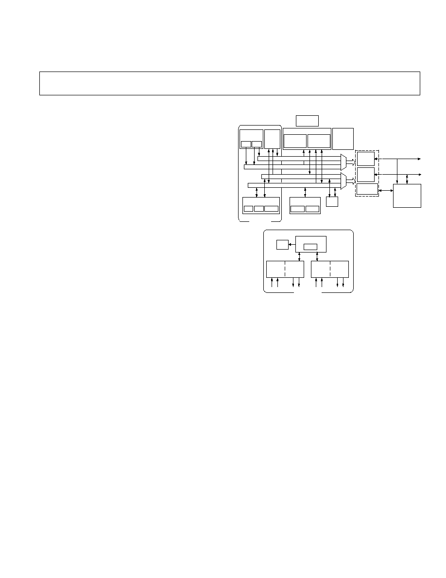
FUNCTIONAL BLOCK DIAGRAM
SERIAL PORTS
SPORT 1
SPORT 0
BYTE DMA
CONTROLLER
EXTERNAL
DATA
BUS
EXTERNAL
ADDRESS
BUS
FULL MEMORY
MODE
MEMORY
PROGRAMMABLE
I/O
AND
FLAGS
16K PM
(OPTIONAL 8K)
TIMER
ADSP-2100 BASE
ARCHITECTURE
SHIFTER
MAC
ALU
ARITHMETIC UNITS
POWER-DOWN
CONTROL
PROGRAM
SEQUENCER
DAG 2
DAG 1
DATA ADDRESS
GENERATORS
PROGRAM MEMORY ADDRESS
DATA MEMORY ADDRESS
PROGRAM MEMORY DATA
DATA MEMORY DATA
16K DM
(OPTIONAL 8K)
SERIAL PORT
REF
ADC1
ADC2
DAC1
DAC2
ANALOG FRONT END
SECTION
SPORT 2
FLASH
Byte Memory
64 kbytes
programmable input/ouput gains with ranges 38 dB and 21
dB respectively. An on-chip reference voltage is included
to allow single supply operation.
The AD73522's DSP engine combines the ADSP-2100
family base architecture (three computational units, data
address generators and a program sequencer) with two serial
ports, a 16-bit internal DMA port, a byte DMA port, a
programmable timer, Flag I/O, extensive interrupt capabilities
and on-chip program and data memory.
The AD73522-80 integrates 80K bytes of on-chip memory
configured as 16K words (24-bit) of program RAM, and 16K
words (16-bit) of data RAM. The AD73522-40 integrates
40K bytes of on-chip memory configured as 8K words (24-
bit) of program RAM, and 8K words (16-bit) of data RAM.
Both devices feature a Flash memory array of 64 kbytes (512
kbits) connected to the DSP's byte-wide DMA port
(BDMA). This allows non-volatile storage of the DSP's boot
code and system data parameters. Power-down circuitry is
also provided to meet the low power needs of battery
operated portable equipment. The AD73522 is available in a
119-ball PBGA package.
AD73522
�2�
REV. PrC 05/99
Preliminary Technical Data
PRELIMINAR
Y
TECHNICAL
DA
TA
ARCHITECTURE OVERVIEW
The AD73522 instruction set provides flexible data moves
and multifunction (one or two data moves with a
computation) instructions. Every instruction can be executed
in a single processor cycle. The AD73522 assembly language
uses an algebraic syntax for ease of coding and readability. A
comprehensive set of development tools supports program
development.
SERIAL PORTS
SPORT 1
SPORT 0
BYTE DMA
CONTROLLER
EXTERNAL
DATA
BUS
EXTERNAL
ADDRESS
BUS
FULL MEMORY
MODE
MEMORY
PROGRAMMABLE
I/O
AND
FLAGS
16K PM
(OPTIONAL 8K)
TIMER
ADSP-2100 BASE
ARCHITECTURE
SHIFTER
MAC
ALU
ARITHMETIC UNITS
POWER-DOWN
CONTROL
PROGRAM
SEQUENCER
DAG 2
DAG 1
DATA ADDRESS
GENERATORS
PROGRAM MEMORY ADDRESS
DATA MEMORY ADDRESS
PROGRAM MEMORY DATA
DATA MEMORY DATA
16K DM
(OPTIONAL 8K)
SERIAL PORT
REF
ADC1
ADC2
DAC1
DAC2
ANALOG FRONT END
SECTION
SPORT 2
FLASH
Byte Memory
64 kbytes
Figure 1. Functional Block Diagram
Figure 1 is an overall block diagram of the AD73522. The
processor section contains three independent computational
units: the ALU, the multiplier/accumulator (MAC) and the
shifter. The computational units process 16-bit data directly
and have provisions to support multiprecision computations.
The ALU performs a standard set of arithmetic and logic
operations; division primitives are also supported. The MAC
performs single-cycle multiply, multiply/add and multiply/
subtract operations with
40 bits of accumulation. The shifter performs logical and
arithmetic shifts, normalization, denormalization and derive
exponent operations.
The internal result (R) bus connects the computational units
so that the output of any unit may be the input of any unit on
the next cycle.
A powerful program sequencer and two dedicated data address
generators ensure efficient delivery of operands to these compu-
tational units. The sequencer supports conditional jumps, sub-
routine calls and returns in a single cycle. With internal loop
counters and loop stacks, the AD73522 executes looped code
with zero overhead; no explicit jump instructions are required to
maintain loops.
Two data address generators (DAGs) provide addresses for
simultaneous dual operand fetches (from data memory and
program memory). Each DAG maintains and updates four
address pointers. Whenever the pointer is used to access data
(indirect addressing), it is post-modified by the value of one
of four possible modify registers. A length value may be
associated with each pointer to implement automatic modulo
addressing for
circular buffers.
The two address buses (PMA and DMA) share a single
external address bus, allowing memory to be expanded off-
chip, and the two data buses (PMD and DMD) share a single
external data bus. Byte memory space and I/O memory space
also share the external buses.
An interface to low cost byte-wide memory is provided by the
Byte DMA port (BDMA port). The BDMA port is
bidirectional and can directly address up to four megabytes of
external RAM or ROM for off-chip storage of program
overlays or data tables.
The AD73522 can respond to eleven interrupts. There can be
up to six external interrupts (one edge-sensitive, two level-
sensitive and three configurable) and seven internal interrupts
generated by the timer, the serial ports (SPORTs), the Byte
DMA port and the power-down circuitry. There is also a
master RESET signal. The two serial ports provide a complete
synchronous serial interface with optional companding in
hardware and a wide variety of framed or frameless data transmit
and receive modes of operation.
Each port can generate an internal programmable serial clock
or accept an external serial clock.
The AD73522 provides up to 13 general-purpose flag pins.
The data input and output pins on SPORT1 can be
alternatively configured as an input flag and an output flag. In
addition, there are eight flags that are programmable as inputs
or outputs and three flags that are always outputs.
A programmable interval timer generates periodic interrupts.
A 16-bit count register (TCOUNT) is decremented every n
processor cycle, where n is a scaling value stored in an 8-bit
register (TSCALE). When the value of the count register
reaches zero, an interrupt is generated and the count register
is reloaded from a 16-bit period register (TPERIOD).
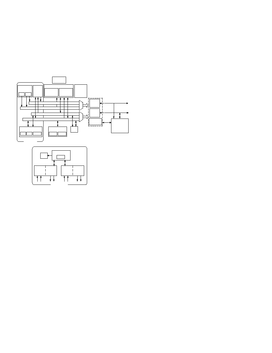
Analog Front End
The AFE section is configured as a separate block which is
normally connected to either SPORT0 or SPORT1 of the
DSP section. As it is not hard-wired to either SPORT the
user has total flexibility in how they wish to allocate system
resources to support the AFE. It is also possible to further
expand the number of analog I/O channels connected to the
SPORT by cascading other single or dual channel AFEs
(AD73311 or AD73322) external to the AD73522.
The AFE is configured as a cascade of two I/O channels
(similar to that of the discrete AD73322 - refer to the
AD73322 datasheet for more details) with each channel
having a separate 16-bit sigma-delta based ADC and DAC.
Both channels share a common reference whose nominal
value is 1.2V. Figure 2 shows a block diagram of the AFE
section of the AD73522. It shows two channels of ADC and
DAC conversion alog with a common reference.
Communication to both channels is handled by the SPORT2
block which interfaces to either SPORT0 or SPORT1 of the
DSP section.
Figure 3 shows the analog connectivity available on each
channel of the AFE (Channel 1 is detailed here). Both
channels feature fully differential inputs and outputs. The
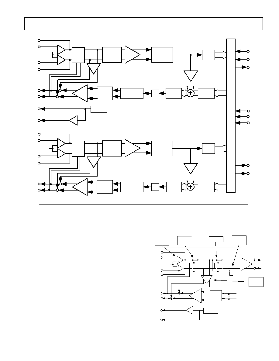
AD73522
�3�
REV. PrC 05/99
Preliminary Technical Data
PRELIMINAR
Y
TECHNICAL
DA
TA
input section allows direct connection to the internal
Programmable Gain Amplifier at the input of the sigma-delta
ADC section or optional inverting amplifiers may be
configured to provide some fixed external gain or to interface
to a transducer with relatively high source impedance. The
input section also features programmable differential channel
inversion and configuration of the the differential input as
two separate single-ended inputs. The ADC features a second
order sigma-delta modulator which samples at MCLK/8. Its
bitstream output is filtered and decimated by a Sinc-cubed
decimator to provide a sample rate selectable from 64 kHz, 32
kHz, 16 kHz or 8 kHz (based on an MCLK of 16.384 MHz).
The DAC channel features a Sinc-cubed interpolator which
increases the sample rate from the selected rate to the digital
sigma-delta modulator rate of MCLK/8. The digital sigma-
delta modulator's output bit-stream is fed to a single-bit DAC
whose output is reconstructed/filtered by two stages of low-
pass filtering (switched capacitor and continuous time) before
being applied to the differential output driver.
Each channel also features two programmable gain elements,
Analog Gain Tap (AGT) and Digital Gain Tap (DGT),
which, when enabled, add a signed and scaled amount of the
input signal to the DAC's output signal. This is of particular
use in line impedance balancing when interfacing the AFE to
Subscriber Line Interface Circuits (SLICs).
VINN1
VINP1
VFBN1
VFBP1
VREF
VOUTP1
VOUTN1
Continuous
Time
Low-Pass
Filter
+6/-15dB
PGA
VREF
Analog
Loopback
select
Single-Ended
Enable
Invert
Inverting Op-
amps
Analog
Gain Tap
Gain
+/- 1
0/38 dB
PGA
REFOUT
REFCAP
Reference
Figure 3: Analog Front End Configuration
+
+
VINN1
VINP1
VFBN1
VFBP
1
VREF
Analog
Sigma-Delta
Modulator
-
+
0/38dB
PGA
VOUTP1
VOUTN1
Continuous
Time
Low-Pass
Filter
+6/-15dB
PGA
+
Switched-
Capacitor
Low Pass Filter
Interpolator
Digital
Sigma-Delta
Modulator
1-Bit
DAC
+
GAIN
+/- 1
-
+
+
-
-
GAIN
+/- 1
Decimator
SDI
SDIFS
SCLK2
Seria
l
I/O
Port
REFCAP
REFOUT
Reference
SE
RESETC
SDOFS
SDO
MCLK
+
+
VINN2
VINP2
VFBN2
VFBP2
VREF
Analog
Sigma-Delta
Modulator
-
+
0/38dB
PGA
VOUTP2
VOUTN2
Continuous
Time
Low-Pass
Filter
+6/-15dB
PGA
+
Switched-
Capacitor
Low Pass Filter
Interpolator
Digital
Sigma-Delta
Modulator
1-Bit
DAC
+
+
-
-
GAIN
+/- 1
Decimator
+
GAIN
+/- 1
-
Invert
Single-Ended
Enable
Analog
Loop
Back
Invert
Single-Ended
Enable
Analog
Loop
Back
Figure 2: Functional Block Diagram of Analog Front End
Section

�4�
REV. PrC 05/99
AD73522�SPECIFICATIONS
PRELIMINAR
Y
TECHNICAL
DA
TA
(AVDD = DVDD = +3.0V to 3.6V; DGND = AGND = 0 V, f
MCLK
= 16.384 MHz,
f
SAMP
= 64 kHz; T
A
= T
MIN
to T
MAX
, unless otherwise noted)
PARAMETER
Min
Typ
Max
Units
Test Conditions
AFE SECTION
REFERENCE
REFCAP
Absolute Voltage, V
REFCAP
1.08
1.2
1.32
V
REFCAP TC
50
ppm/�C 0.1 �F Capacitor Required from
REFOUT
REFCAP to AGND2
Typical Output Impedance
130
W
Absolute Voltage, V
REFOUT
1.08
1.2
1.32
V
Unloaded
Minimum Load Resistance
1
kW
Maximum Load Capacitance
100
pF
INPUT AMPLIFIER
Offset
�1.0
mV
Maximum Output swing
1.578
V
Max. Output Swing =(1.578/1.2)*V
REFCAP
Feedback Resistance
50
kW
f
C
= 32 kHz
Feedback Capacitance
100
pF
ANALOG GAIN TAP
Gain at Max. Setting
+1
Gain at Min. Setting
-1
Gain Resolution
5
Bits
Gain Step Size = 0.0625
Gain Accuracy
�1.0
%
Output Unloaded
Settling Time
1.0
ms
Tap Gain Change of -FS to +FS
Delay
0.5
ms
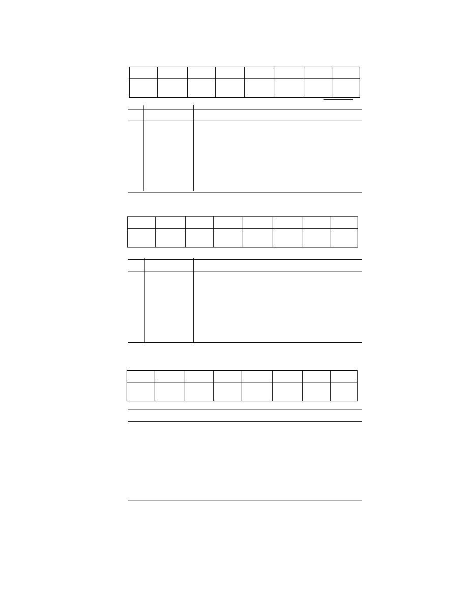
ADC SPECIFICATIONS
Maximum Input Range at VIN
2, 3
1.578
V p-p
Measured Differentially.
�2.85
dBm
Max. Input = (1.578/1.2)*V
REFCAP
Nominal Reference Level at VIN
1.0954
V p-p
Measured Differentially
(0 dBm0)
�6.02
dBm
Absolute Gain
PGA = 0 dB
�0.5
0.4
+1.2 dB
1.0 kHz, 0 dBm0
PGA = 38 dB
�1.5
�0.7
+0.1 dB
1.0 kHz, 0 dBm0
Gain Tracking Error
�0.1
dB
1.0 kHz, +3 dBm0 to �50 dBm0
Signal to (Noise + Distortion)
Refer to Figure 5
PGA = 0 dB
72
78
dB
300 Hz to 3400 Hz; f
SAMP
= 64 kHz
78
dB
300 Hz to 3400 Hz; f
SAMP
= 8 kHz
55
57
dB
0 Hz to f
SAMP
/2; f
SAMP
= 64 kHz
PGA = 38 dB
52
56
dB
300 Hz to 3400 Hz; f
SAMP
= 64 kHz
Total Harmonic Distortion
PGA = 0 dB
�84
�73
dB
300 Hz to 3400 Hz; f
SAMP
= 64 kHz
PGA = 38 dB
�70
�60
dB
300 Hz to 3400 Hz; f
SAMP
= 64 kHz
Intermodulation Distortion
�65
dB
PGA = 0 dB
Idle Channel Noise
�71
dBm0
PGA = 0 dB
Crosstalk, ADC-to-DAC
�100
dB
ADC Input Level: 1.0kHz, 0 dBm0
DAC Input at Idle
ADC-to-ADC
-100
dB
ADC1 Input Level: 1.0kHz, 0 dBm0
ADC2 Input at Idle. Input Amps bypassed
-70
dB
Input Amplifiers included in input channel
DC Offset
�30
+10
+45
mV
PGA = 0 dB
Power Supply Rejection
�65
dB
Input Signal Level at AVDD and DVDD
Pins: 1.0 kHz, 100 mV p-p Sine Wave
Group Delay
4, 5
25
�s
Input Resistance at PGA
2, 4, 6
20
kW
DMCLK = 16.384 MHz; Input Amplifiers
bypassed and AGT off
DIGITAL GAIN TAP
Gain at Max. Setting
+1
Gain at Min. Setting
-1
Gain Resolution
16
Bits
Tested to 5 MSBs of settings
Delay
25
ms
Includes DAC delay
Settling Time
100
ms
Tap Gain Change from -FS to +FS;
Includes DAC settling time

�5�
REV. PrC 05/99
AD73522
Preliminary Technical Data
PRELIMINAR
Y
TECHNICAL
DA
TA
PARAMETER
Min
Typ
Max
Units
Test Conditions (STYLE: table col.head)
DAC SPECIFICATIONS
Maximum Voltage Output Swing
2
Single Ended
1.578
V p-p
PGA = 6 dB
�2.85
dBm
Max. Output = (1.578/1.2)*V
REFCAP
Differential
3.156
V p-p
PGA = 6 dB
3.17
dBm
Max. Output = 2*((1.578/1.2)*V
REFCAP
)
Nominal Voltage Output Swing (0 dBm0)
Single-Ended
1.0954
V p-p
PGA = 6 dB
�6.02
dBm
Differential
2.1909
V p-p
PGA = 6 dB
0
dBm
Output Bias Voltage
1.2
V
REFOUT Unloaded
Absolute Gain
�0.5
+0.4
+1.2 dB
1.0 kHz, 0 dBm0; Unloaded
Gain Tracking Error
� 0.1
dB
1.0 kHz, +3 dBm0 to �50 dBm0
Signal to (Noise + Distortion) at 0 dBm0
Refer to Figure 6: AV
DD
= 3.00V +/- 5%
PGA = 6 dB
62.5
77
dB
300 Hz to 3400 Hz; f
SAMP
= 64 kHz
Total Harmonic Distortion at 0 dBm0
AV
DD
= 3.00V +/- 5%
PGA = 6 dB
-80
�62.5 dB
300 Hz to 3400 Hz; f
SAMP
= 64 kHz
Intermodulation Distortion
�85
dB
PGA = 0 dB
Idle Channel Noise
�85
dBm0
PGA = 0 dB
Crosstalk, DAC-to-ADC
�90
dB
ADC Input Level: AGND;
DAC Output Level: 1.0 kHz, 0 dBm0;
Input Amplifiers bypassed
-77
dB
Input amplifiers included in input channel
DAC-to-DAC
�100
dB
DAC1Output Level:AGND;
DAC2 Output Level: 1.0 kHz, 0 dBm0
Power Supply Rejection
�65
dB
Input Signal Level at AVDD and DVDD
Pins: 1.0 kHz, 100 mV p-p Sine Wave
Group Delay
4, 5
25
�s
Interpolator Bypassed
50
�s
Output DC Offset
2, 7
�20
+12
+45
mV
Minimum Load Resistance, R
L
2, 8
Single-Ended
4
150
W
Differential
150
W
Maximum Load Capacitance, C
L
2, 8
Single-Ended
4
500
pF
Differential
100
pF
LOGIC INPUTS
V
INH
, Input High Voltage
DVDD � 0.8
DVDD
V
V
INL
, Input Low Voltage
0
0.8
V
I
IH
, Input Current
-10
+10
�A
C
IN
, Input Capacitance
10
pF
LOGIC OUTPUT
V
OH
, Output High Voltage
DVDD � 0.4
DVDD
V
|IOUT| - 100 �A
V
OL
, Output Low Voltage
0
0.4
V
|IOUT| - 100 �A
Three-State Leakage Current
�10
+10
�A
POWER SUPPLIES
AVDD1, AVDD2
3.0
3.6
V
DVDD
3.0
3.6
V
I
DD
10
See Table I
NOTES
1
Operating temperature range is as follows: �20�C to +85�C. Therefore, T
MIN
= �20�C and T
MAX
= +85�C.
2
Test conditions: Input PGA set for 0 dB gain, Output PGA set for 6 dB gain, no load on analog outputs (unless otherwise noted).
3
At input to sigma-delta modulator of ADC.
4
Guaranteed by design.
5
Overall group delay will be affected by the sample rate and the external digital filtering.
6
The ADC's input impedance is inversely proportional to DMCLK and is approximated by: (3.3
10
11
)/DMCLK.
7
Between VOUTP1 and VOUTN1 or between VOUTP2 and VOUTN2.
8
At VOUT output.
9
Frequency responses of ADC and DAC measured with input at audio reference level (the input level that produces an output level of �10 dBm0), with 38 dB preamplifier
bypassed and input gain of 0 dB.
10
Test Conditions: no load on digital inputs, analog inputs ac coupled to ground, no load on analog outputs.
Specifications subject to change without notice.

�6�
REV. PrC 05/99
AD73522�SPECIFICATIONS
PRELIMINAR
Y
TECHNICAL
DA
TA
(AVDD = DVDD = +3.0V to 3.6V; DGND = AGND = 0 V, f
MCLK
= 16.384 MHz,
f
SAMP
= 64 kHz; T
A
= T
MIN
to T
MAX
, unless otherwise noted)
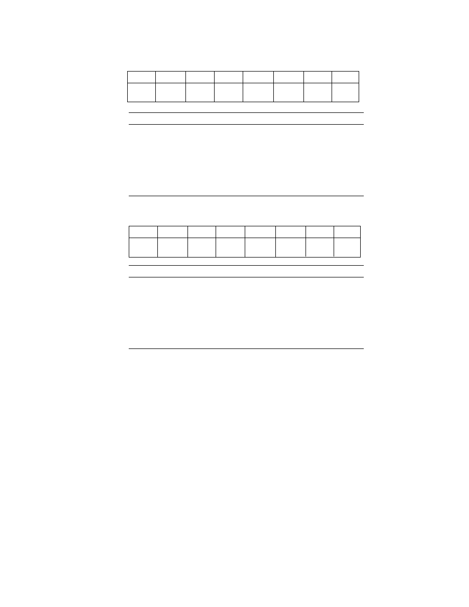
PARAMETER
Test Conditions
Min
Typ
Max
Unit
DSP SECTION
V
IH
Hi-Level Input Voltage
1, 2
@ V
DD
= max
2.0
V
V
IH
Hi-Level CLKIN Voltage
@ V
DD
= max
2.2
V
V
IL
Lo-Level Input Voltage
1, 3
@ V
DD
= min
0.8
V
V
OH
Hi-Level Output Voltage
1, 4, 5
@ V
DD
= min
I
OH
= �0.5 mA
2.4
V
@ V
DD
= min
I
OH
= �100 �A
6
V
DD
� 0.3
V
V
OL
Lo-Level Output Voltage
1, 4, 5
@ V
DD
= min
I
OL
= 2 mA
0.4
V
I
IH
Hi-Level Input Current
3
@ V
DD
= max
V
IN
= V
DD
max
10
�A
I
IL
Lo-Level Input Current
3
@ V
DD
= max
V
IN
= 0 V
10
�A
I
OZH
Three-State Leakage Current
7
@ V
DD
= max
V
IN
= V
DD
max
8
10
�A
I
OZL
Three-State Leakage Current
7
@ V
DD
= max
V
IN
= 0 V
8
10
�A
I
DD
Supply Current (Idle)
9
@ V
DD
= 3.3
t
CK
= 19 ns
10
10
mA
t
CK
= 25 ns
10
8
mA
t
CK
= 30 ns
10
7
mA
I
DD
Supply Current (Dynamic)
11
@ V
DD
= 3.3
T
AMB
= +25�C
t
CK
= 19 ns
10
51
mA
t
CK
= 25 ns
10
41
mA
t
CK
= 30 ns
10
34
mA
C
I
Input Pin Capacitance
3, 6, 12
@ V
IN
= 2.5 V
f
IN
= 1.0 MHz
T
AMB
= +25�C
8
pF
C
O
Output Pin Capacitance
6, 7, 12, 13
@ V
IN
= 2.5 V
f
IN
= 1.0 MHz
T
AMB
= +25�C
8
pF
NOTES
1
1
Bidirectional pins: D0�D23, RFS0, RFS1, SCLK0, SCLK1, TFS0, TFS1, A1�A13, PF0�PF7.
1
2
Input only pins: RESET, BR, DR0, DR1, PWD.
1
3
Input only pins: CLKIN, RESET, BR, DR0, DR1, PWD.
1
4
Output pins: BG, PMS, DMS, BMS, IOMS, CMS, RD, WR, PWDACK, A0, DT0, DT1, CLKOUT, FL2�0, BGH.
1
5
Although specified for TTL outputs, all AD73522 outputs are CMOS-compatible and will drive to V
DD
and GND, assuming no dc loads.
1
6
Guaranteed but not tested.
1
7
Three-statable pins: A0�A13, D0�D23, PMS, DMS, BMS, IOMS, CMS, RD, WR, DT0, DT1, SCLK0, SCLK1, TFS0, TFS1, RFS0, RFS1, PF0�PF7.
1
8
0 V on BR.
1
9
Idle refers to AD73522 state of operation during execution of IDLE instruction. Deasserted pins are driven to either
V
DD
or GND.
10
V
IN
= 0 V and 3 V. For typical figures for supply currents, refer to Power Dissipation section.
11
I
DD
measurement taken with all instructions executing from internal memory. 50% of the instructions are multifunction (types 1, 4, 5, 12, 13, 14), 30% are type 2
and type 6, and 20% are idle instructions.
12
Applies to PBGA package type.
13
Output pin capacitance is the capacitive load for any three-stated output pin.
Specifications subject to change without notice.

�7�
REV. PrC 05/99
AD73522
Preliminary Technical Data
PRELIMINAR
Y
TECHNICAL
DA
TA
POWER CONSUMPTION
CONDITIONS
Typ.
Max.
SE
MCLK On
Test Conditions
AFE SECTION
ADCs On Only
11.5
12
1
YES
REFOUT Disabled
DACs On Only
20
22
1
YES
REFOUT Disabled
ADCs and DACs On
24.5
27
1
YES
REFOUT Disabled
ADCs and DACs
30
34
1
YES
REFOUT Disabled
and Input Amps On
ADCs and DACs
29
32.5
1
YES
REFOUT Disabled
and AGT On
All Sections On
37
42
1
YES
REFCAP On Only
0.8
1.25
0
NO
REFOUT Disabled
REFCAP and
3.5
4.5
0
NO
REFOUT On Only
All AFE Sections Off
1.5
1.8
0
YES
MCLK Active Levels Equal to 0V
and DVDD
All AFE Sections Off
10 �A
40 �A
0
NO
Digital Inputs Static and Equal to
0 V or DVDD
Flash SECTION
Read Mode
12
BMS = RD = 0; WR = 1
Write Mode
15
BMS = WR = 0; RD = 1
Standby Current
15
�
A
BMS = RD = WR = 1
The above values are in mA and are typical values unless otherwise noted.
TIMING CHARACTERISTICS - AFE SECTION
Parameter
Limit
Units
Description
Clock Signals
See Figure 1
t
1
61
ns min 16.384 MHz MCLK Period
t
2
24.4
ns min MCLK Width High
t
3
24.4
ns min MCLK Width Low
Serial Port
See Figures 3 and 4
t
4
t
1
ns min SCLK Period (SCLK = MCLK)
t
5
0.4 * t
1
ns min SCLK Width High
t
6
0.4 * t
1
ns min SCLK Width Low
t
7
20
ns min SDI/SDIFS Setup Before SCLK Low
t
8
0
ns min SDI/SDIFS Hold After SCLK Low
t
9
10
ns max SDOFS Delay From SCLK High
t
10
10
ns min SDOFS Hold After SCLK High
t
11
10
ns min SDO Hold After SCLK High
t
12
10
ns max SDO Delay From SCLK High
AD73522
�8�
REV. PrC 05/99
Preliminary Technical Data
PRELIMINAR
Y
TECHNICAL
DA
TA
A
B
C
D
E
F
G
H
J
K
L
M
N
P
R
T
U
A
B
C
D
E
F
G
H
J
K
L
M
N
P
R
T
U
1 2 3 4 5 6 7
1 2 3 4 5 6 7
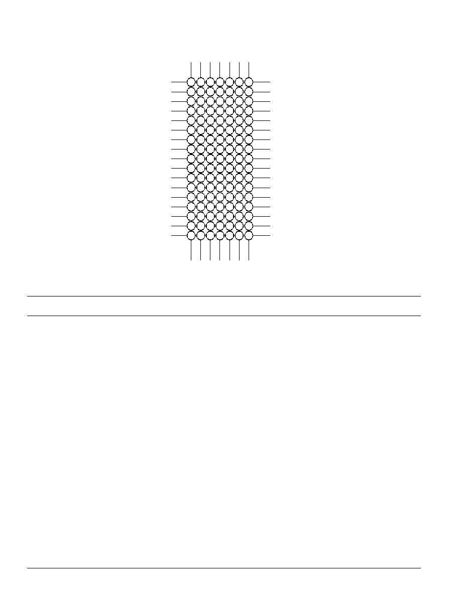
PBGA Ball Configurations
PBGA
Ball
PBGA
Ball
PBGA
Ball
PBGA
Ball
Number
Name
Number
Name
Number
Name
Number
Name
A1
IRQE/PF4
E3
RFS0
J5
D22
N7
D13
A2
DMS
E4
A3/IAD2
J6
D21
P1
EBR
A3
VDD(INT)
E5
A2/IAD1
J7
D20
P2
D0/IAD13
A4
CLKIN
E6
A1/IAD0
K1
ELOUT
P3
DVDD
A5
A11/IAD10
E7
A0
K2
ELIN
P4
DGND
A6
A7/IAD6
F1
DR0
K3
EINT
P5
RESETC
A7
A4/IAD3
F2
SCLK0
K4
D19
P6
SCLK2
B1
IRQL0/PF5
F3
DT1
K5
D18
P7
MCLK
B2
PMS
F4
PWDACK
K6
D17
R1
SDO
B3
WR
F5
BGH
K7
D16
R2
SDOFS
B4
XTAL
F6
PF0[MODE A]
L1
BG
R3
SDIFS
B5
A12/IAD11
F7
PF1[MODE B]
L2
D3/
IACK
R4
SDI
B6
A8/IAD7
G1
TFS1
L3
D5/IAL
R5
SE
B7
A5/IAD4
G2
RFS1
L4
D8
R6
REFCAP
C1
IRQL1/PF6
G3
DR1
L5
D9
R7
REFOUT
C2
IOMS
G4
GND
L6
D12
T1
VFBP1
C3
RD
G5
PWD
L7
D15
T2
VINP1
C4
VDD(EXT)
G6
VDD(EXT)
M1
EBG
T3
VFBN1
C5
A13/IAD12
G7
PF2[MODE C]
M2
D2/IAD15
T4
VINN1
C6
A9/IAD8
H1
SCLK1
M3
D4/
IS
T5
VFBN2
C7
GND
H2
ERESET
M4
D7/
IWR
T6
VINN2
D1
IRQ2/PF7
H3
RESET
M5
VDD(EXT)
T7
VFBP2
D2
CMS
H4
PF3
M6
D11
U1
AGND
D3
BMS
H5
FL0
M7
D14
U2
AVDD
D4
CLKOUT
H6
FL1
N1
BR
U3
VOUTP2
D5
GND
H7
FL2
N2
D1/IAD14
U4
VOUTN2
D6
A10/IAD9
J1
EMS
N3
VDD(INT)
U5
VOUTP1
D7
A6/IAD5
J2
EE
N4
D6/
IRD
U6
VOUTN1
E1
DT0
J3
ECLK
N5
GND
U7
VINP2
E2
TFS0
J4
D23
N6
D10

AD73522
�9�
REV. PrC 05/99
Preliminary Technical Data
PRELIMINAR
Y
TECHNICAL
DA
TA
ORDERING GUIDE
Temperature
Package
Package
Model
Range
Description
Option
AD73522-80
-20 C to +85 C
119-Ball Plastic Ball Grid Array
B-119
AD73522-40
-20 C to +85 C
119-Ball Plastic Ball Grid Array
B-119
CAUTION
ESD (electrostatic discharge) sensitive device. Electrostatic charges as high as 4000 V readily
accumulate on the human body and test equipment and can discharge without detection.
Although the AD73522 features proprietary ESD protection circuitry, permanent damage may
occur on devices subjected to high energy electrostatic discharges. Therefore, proper ESD
precautions are recommended to avoid performance degradation or loss of functionality.

AD73522
�10�
REV. PrC 05/99
Preliminary Technical Data
PRELIMINAR
Y
TECHNICAL
DA
TA
PIN FUNCTION DESCRIPTION
Mnemonic
Function
VINP1
Analog Input to the inverting terminal of the inverting input amplifier on Channel 1's Positive Input.
VFBP1
Feedback connection from the output of the inverting amplifier on Channel 1's positive input. When the input
amplifiers are bypassed, this pin allows direct access to the positive input of Channel 1's sigma delta modulator.
VINN1
Analog Input to the inverting terminal of the inverting input amplifier on Channel 1's Negative Input.
VFBN1
Feedback connection from the output of the inverting amplifier on Channel 1's negative input. When the input
amplifiers are bypassed, this pin allows direct access to the negative input of Channel 1's sigma delta modulator.
REFOUT
Buffered Reference Output, which has a nominal value of 1.2 V.
REFCAP
A Bypass Capacitor to AGND2 of 0.1 �F is required for the on-chip reference. The capacitor should be fixed to
this pin.
AVDD2
Analog Power Supply Connection for Codec 2.
AGND2
Analog Ground/Substrate Connection for Codec 2.
DGND
Digital Ground/Substrate Connection.
DVDD
Digital Power Supply Connection.
RESET
Active Low Reset Signal. This input resets the entire chip, resetting the control registers and clearing the digital
circuitry.
SCLK
Output Serial Clock whose rate determines the serial transfer rate to/from the codec. It is used to clock data or
control information to and from the serial port (SPORT). The frequency of SCLK is equal to the frequency of
the master clock (MCLK) divided by an integer number--this integer number being the product of the external
master clock rate divider and the serial clock rate divider.
MCLK
Master Clock Input. MCLK is driven from an external clock signal.
SDO
Serial Data Output of the Codec. Both data and control information may be output on this pin and is clocked on
the positive edge of SCLK. SDO is in three-state when no information is being transmitted and when SE is low.
SDOFS
Framing Signal Output for SDO Serial Transfers. The frame sync is one-bit wide and it is active one SCLK
period before the first bit (MSB) of each output word. SDOFS is referenced to the positive edge of SCLK.
SDOFS is in three-state when SE is low.
SDIFS
Framing Signal Input for SDI Serial Transfers. The frame sync is one-bit wide and it is valid one SCLK period
before the first bit (MSB) of each input word. SDIFS is sampled on the negative edge of SCLK and is ignored
when SE is low.
SDI
Serial Data Input of the Codec. Both data and control information may be input on this pin and are clocked on
the negative edge of SCLK. SDI is ignored when SE is low.
SE
SPORT Enable. Asynchronous input enable pin for the SPORT. When SE is set low by the DSP, the output pins
of the SPORT are three-stated and the input pins are ignored. SCLK is also disabled internally in order to
decrease power dissipation. When SE is brought high, the control and data registers of the SPORT are at their
original values (before SE was brought low), however the timing counters and other internal registers are at their
reset values.
AGND1
Analog Ground/Substrate Connection for Codec 1.
AVDD1
Analog Power Supply Connection for Codec 1.
VOUTP2
Analog Output from the Positive Terminal of Output Channel 2.
VOUTN2
Analog Output from the Negative Terminal of Output Channel 2.
VOUTP1
Analog Output from the Positive Terminal of Output Channel 1.
VOUTN1
Analog Output from the Negative Terminal of Output Channel1.
VINP2
Analog Input to the inverting terminal of the inverting input amplifier on Channel 2's Positive Input.
VFBP2
Feedback connection from the output of the inverting amplifier on Channel 2's positive input. When the input
amplifiers are bypassed, this pin allows direct access to the positive input of Channel 2's sigma delta modulator.
VINN2
Analog Input to the inverting terminal of the inverting input amplifier on Channel 2's Negative Input.
VFBN2
Feedback connection from the output of the inverting amplifier on Channel 2's negative input. When the input
amplifiers are bypassed, this pin allows direct access to the negative input of Channel 2's sigma delta modulator.
RESET
(Input) Processor Reset Input
BR
(Input) Bus Request Input
BG
(Output) Bus Grant Output
BGH
(Output) Bus Grant Hung Output
DMS
(Output) Data Memory Select Output
PMS
(Output) Program Memory Select Output
IOMS
(Output) Memory Select Output
BMS
(Output) Byte Memory Select Output
CMS
(Output) Combined Memory Select Output
RD
(Output) Memory Read Enable Output
WR
(Output) Memory Write Enable Output

AD73522
�11�
REV. PrC 05/99
Preliminary Technical Data
PRELIMINAR
Y
TECHNICAL
DA
TA
IRQ2/
(Input) Edge- or Level-Sensitive Interrupt
PF7
(Input/Output) Request.
1
Programmable I/O Pin
IRQL0/
(Input) Level-Sensitive Interrupt Requests
1
PF6
(Input/Output) Programmable I/O Pin
IRQL1/
(Input) Level-Sensitive Interrupt Requests
1
PF5
(Input/Output) Programmable I/O Pin
IRQE/
(Input) Edge-Sensitive Interrupt Requests
1
PF4
(Input/Output) Programmable I/O Pin
Mode D/
(Input) Mode Select Input--Checked Only During RESET
PF3
(Input/Output) Programmable I/O Pin During Normal Operation
Mode C/
(Input) Mode Select Input--Checked Only During RESET
PF2
(Input/Output) Programmable I/O Pin During Normal Operation
Mode B/
(Input) Mode Select Input--Checked Only During RESET
PF1
(Input/Output) Programmable I/O Pin During Normal Operation
Mode A/
(Input) Mode Select Input--Checked Only During RESET
PF0
(Input/Output) Programmable I/O Pin During Normal Operation
CLKIN,
XTAL
(Inputs) Clock or Quartz Crystal Input
CLKOUT
(Output) Processor Clock Output
SPORT0
(Inputs/Outputs) Serial Port I/O Pins
SPORT1
(Inputs/Outputs) Serial Port I/O Pins
IRQ1:0
(Inputs) Edge- or Level-Sensitive Interrupts,
FI
(Input) Flag In
2
FO
(Output) Flag Out
2
PWD
(Input) Power-Down Control Input
PWDACK
(Output) Power-Down Control Output
FL0, FL1,
FL2
(Outputs) Output Flags
VDD and
GND
Power and Ground
EZ-Port
(Inputs/Outputs) For Emulation Use
AD73522
�12�
REV. PrC 05/99
Preliminary Technical Data
PRELIMINAR
Y
TECHNICAL
DA
TA
FUNCTIONAL DESCRIPTION - AFE
Encoder Channels
Both encoder channels consist of a pair of inverting op-amps
with feedback connections which can be bypassed if required,
a switched capacitor PGA and a sigma-delta analog-to-digital
converter (ADC). An on-board digital filter, which forms part
of the sigma-delta ADC, also performs critical system-level
filtering. Due to the high level of oversampling, the input
antialias requirements are reduced such that a simple single
pole RC stage is sufficient to give adequate attenuation in the
band of interest.
Programmable Gain Amplifier
Each encoder section's analog front end comprises a switched
capacitor PGA which also forms part of the sigma-delta
modulator. The SC sampling frequency is DMCLK/8. The
PGA, whose programmable gain settings are shown in Table
I, may be used to increase the signal level applied to the ADC
from low output sources such as microphones, and can be
used to avoid placing external amplifiers in the circuit. The
input signal level to the sigma-delta modulator should not
exceed the maximum input voltage permitted.
The PGA gain is set by bits IGS0, IGS1 and IGS2 (CRD:0�
2) in control register D.
Table I. PGA Settings for the Encoder Channel
IGS2
IGS1
IGS0
Gain (dB)
0
0
0
0
0
0
1
6
0
1
0
12
0
1
1
18
1
0
0
20
1
0
1
26
1
1
0
32
1
1
1
38
ADC
Both ADCs consist of an analog sigma-delta modulator and a
digital antialiasing decimation filter. The sigma-delta
modulator noise-shapes the signal and produces 1-bit
samples at a DMCLK/8 rate. This bit-stream, representing
the analog input signal, is input to the antialiasing decimation
filter. The decimation filter reduces the sample rate and
increases the resolution.
Analog Sigma-Delta Modulator
The AD73522's input channels employ a sigma-delta
conversion technique, which provides a high resolution 16-bit
output with system filtering being implemented on-chip.
Sigma-delta converters employ a technique known as
oversampling where the sampling rate is many times the
highest frequency of interest. In the case of the AD73522, the
initial sampling rate of the sigma-delta modulator is DMCLK/
8. The main effect of oversampling is that the quantization
noise is spread over a very wide bandwidth, up to F
S
/2 =
DMCLK/16 (Figure 4a). This means that the noise in the
band of interest is much reduced. Another complementary
feature of sigma-delta converters is
the use of a technique called noise-shaping. This technique
has the effect of pushing the noise from the band of interest
to an out-of-band position (Figure 4b). The combination of
these techniques, followed by the application of a digital filter,
reduces the noise in band sufficiently to ensure good dynamic
performance from the part (Figure 4c).
BAND
OF
INTEREST
FS/2
DMCLK/16
a.
BAND
OF
INTEREST
NOISE SHAPING
FS/2
DMCLK/16
b.
BAND
OF
INTEREST
FS/2
DMCLK/16
DIGITAL FILTER
c.
Figure 4. Sigma-Delta Noise Reduction
Figure 5 shows the various stages of filtering that are
employed in a typical AD73522 application. In Figure 5a we
see the transfer function of the external analog antialias filter.
Even though it is a single RC pole, its cutoff frequency is
sufficiently far away from the initial sampling frequency
(DMCLK/8) that it takes care of any signals that could be
aliased by the sampling frequency. This also shows the major
difference between the initial oversampling rate and the
bandwidth of interest. In Figure 5b, the signal and noise
shaping responses of the sigma-delta modulator are shown.
The signal response provides further rejection of any high
frequency signals while the noise shaping will push the
inherent quantization noise to an out-of-band position. The
detail of Figure 5c shows the response of the digital
decimation filter (Sinc-cubed response) with nulls every
multiple of DMCLK/256, which corresponds to the
decimation filter update rate for a 64kHz sampling. The nulls
of the Sinc3 response correspond with multiples of the chosen
sampling frequency. The final detail in Figure 5d shows the
application of a final antialias filter in the DSP engine. This
has the advantage of being implemented according to the
user's requirements and available MIPS. The filtering in
Figures 5a through 5c is implemented in the AD73522.
AD73522
�13�
REV. PrC 05/99
Preliminary Technical Data
PRELIMINAR
Y
TECHNICAL
DA
TA
F
B
= 4kHz
FS
INIT
= DMCLK/8
a. Analog Antialias Filter Transfer Function
F
B
= 4kHz
FS
INIT
= DMCLK/8
SIGNAL TRANSFER FUNCTION
NOISE TRANSFER FUNCTION
b. Analog Sigma-Delta Modulator Transfer Function
F
B
= 4kHz
FS
INTER
= DMCLK/256
c. Digital Decimator Transfer Function
F
B
= 4kHz
FS
FINAL
= 8kHz
FS
INTER
= DMCLK/256
d. Final Filter LPF (HPF) Transfer Function
Figure 5. AD73522 ADC Frequency Responses
Decimation Filter
The digital filter used in the AD73522's AFE section carries
out two important functions. Firstly, it removes the out-of-band
quantization noise, which is shaped by the analog modulator
and secondly, it decimates the high frequency bit-stream to a
lower rate 16-bit word.
The antialiasing decimation filter is a sinc-cubed digital filter
that reduces the sampling rate from DMCLK/8 to DMCLK/
256, and increases the resolution from a single bit to 15 bits
or greater (depending on chosen sampling rate). Its Z trans-
form is given as: [(1�Z
�N
)/(1�Z
�1
)]
3
where N is set by the
sampling rate (N= 32 @ 64kHz sampling .... N = 256 @ 8
kHz sampling) Thus when the sampling rate is 64kHz a
minimal group delay of 25 �s can be achieved.
Word growth in the decimator is determined by the sampling
rate. At 64kHz sampling, where the over sampling ratio
between sigma-delta modulator and decimator output equals
32, we get 5 bits per stage of the three stage Sinc3 filter. Due
to symmetry within the sigma delta modulator, the lsb will
always be a zero, therefore the 16 bit ADC output word will
have 2 lsbs equal to zero, one due to the sigma-delta
symmetry and the other being a padding zero to make up the
16 bit word. At lower sampling rates, decimator word growth
will be greater than the 16 bit sample word therefore
truncation occurs in transferring the decimator output as the
ADC word. For example at 8 kHz sampling, word growth
reaches 24 bits due to the OSR of 256 between sigma delta
modulator and decimator output. This yields 8 bits per stage
of the 3 stage Sinc3 filter.
ADC Coding
The ADC coding scheme is in twos complement format (see
Figure 6). The output words are formed by the decimation
filter, which grows the word length from the single-bit output
of the sigma-delta modulator to a word length of up to 18-
bits (depending on decimation rate chosen), which is the final
output of the ADC block. In Data Mode this value is
truncated to 16-bits for output on the Serial data Output
(SDO) pin.
For input values equal to or greater than positive
full scale, however, the output word is set at 0x7FFF, which
has the LSB set to 1
. In mixed Control/Data Mode, the
resolution is fixed at 15 bits, with the MSB of the
16-bit transfer being used as a flag bit to indicate either
control or data in the frame.
V
INN
V
INP
V
REF
+ (V
REF
x 0.32875)
V
REF
V
REF
> (V
REF
x 0.32875)
10...00
00...00
01...11
ADC CODE DIFFERENTIAL
V
INN
V
INP
V
REF
+ (V
REF
x 0.6575)
V
REF
V
REF
> (V
REF
x 0.6575)
10...00
00...00
01...11
ADC CODE SINGLE ENDED
ANALOG
INPUT
ANALOG
INPUT
Figure 6. ADC Transfer Function
Decoder Channel
The decoder channels consist of digital interpolators, digital
sigma-delta modulators, single bit digital-to-analog converters
(DAC), analog smoothing filters and programmable gain
amplifiers with differential outputs.
DAC Coding
The DAC coding scheme is in twos complement format with
0x7FFF being full-scale positive and 0x8000 being full-scale
negative.
Interpolation Filter
The anti-imaging interpolation filter is a sinc-cubed digital
filter which up-samples the 16-bit input words from the
input sample rate to a rate of DMCLK/8 while filtering to
AD73522
�14�
REV. PrC 05/99
Preliminary Technical Data
PRELIMINAR
Y
TECHNICAL
DA
TA
attenuate images produced by the interpolation process. Its Z
transform is given as: [(1�Z
�N
)/(1�Z
�1
)]
3
where n is
determined by the sampling rate (N = 32 @ 64kHz ... N =
256 @ 8kHz). The DAC receives 16-bit samples from the
host DSP processor at the programmed sample rate of
DMCLK/N. If the host processor fails to write a new value to
the serial port, the existing (previous) data is read again. The
data stream is filtered by the anti-imaging interpolation filter,
but there is an option to bypass the interpolator for the
minimum group delay configuration by setting the IBYP bit
(CRE:5) of Control register E. The interpolation filter has the
same characteristics as the ADC's antialiasing decimation
filter.
The output of the interpolation filter is fed to the DAC's
digital sigma-delta modulator, which converts the 16-bit data
to 1-bit samples at a rate of DMCLK/8. The modulator
noise-shapes the signal so that errors inherent to the process
are minimized in the passband of the converter. The bit-
stream output of the sigma-delta modulator is fed to the
single bit DAC where it is converted to an analog voltage.
Analog Smoothing Filter & PGA
The output of the single-bit DAC is sampled at DMCLK/8,
therefore it is necessary to filter the output to reconstruct the
low frequency signal. The decoder's analog smoothing filter
consists of a continuous-time filter preceded by a third-order
switched-capacitor filter. The continuous-time filter forms
part of the output programmable gain amplifier (PGA). The
PGA can be used to adjust the output signal level from �15
dB to +6 dB in 3 dB steps, as shown in Table II. The PGA
gain is set by bits OGS0, OGS1 and OGS2 (CRD:4-6) in
Control Register D.
Table II. PGA Settings for the Decoder Channel
OG2
OG1
OG0
Gain (dB)
0
0
0
+6
0
0
1
+3
0
1
0
0
0
1
1
�3
1
0
0
�6
1
0
1
�9
1
1
0
�12
1
1
1
�15
Differential Output Amplifiers
The decoder has a differential analog output pair (VOUTP
and VOUTN). The output channel can be muted by setting
the MUTE bit (CRD:7) in Control Register D. The output
signal is dc-biased to the codec's on-chip voltage reference.
Voltage Reference
The AD73522 reference, REFCAP, is a bandgap reference
that provides a low noise, temperature-compensated reference
to the DAC and ADC. A buffered version of the reference is
also made available on the REFOUT pin and can be used to
bias other external analog circuitry. The reference has a
nominal value of 1.2 V.
The reference output (REFOUT) can be enabled for biasing
external circuitry by setting the RU bit (CRC:6) of CRC.
VINN1
VINP1
VFBN1
VFBP1
V
REF
VOUTP1
VOUTN1
Continuous
Time
Low-Pass
Filter
+6/-15dB
PGA
V
REF
AD73422
AFE
SECTION
Analog
Loopback
select
Single-Ended
Enable
Invert
Inverting Op-
amps
Analog Gain
Tap
Gain
+/- 1
0/38 dB
PGA
REFOUT
REFCAP
Reference
Figure 7. Analog Input/Output Section
Analog and Digital Gain Taps
The AD73522 features analog and digital feedback paths
between input and output. The amount of feedback is deter-
mined by the gain setting which is programmed in the control
registers. This feature can typically be used for balancing the
effective impedance between input and output when used in
Subscriber Line Interface Circuit (SLIC) interfacing.
Analog Gain Tap
The analog gain tap is configured as a programmable differen-
tial amplifier whose input is taken from the ADC's input
signal path. The output of the analog gain tap is summed with
the output of the DAC. The gain is programmable using
Control Register F (CRF:0-4) to achieve a gain of -1 to +1 in
32 steps with muting being achieved through a separate
control setting (Control Register F Bit _). The gain increment
per step is 0.0625. The AGT is enabled by powering-up the
AGT control bit in the power control register (CRC:1).
When this bit is set (=1) CRF becomes an AGT control
register with CRF:0-4 holding the AGT coefficient, CRF:5
becomes an AGT enable and CRF:7 becomes an AGT mute
control bit. Control bit CRF:5 connects/disconnects the AGT
output to the summer block at the output of the DAC section
while control bit CRF:7 overides the gain tap setting with a
mute, or zero gain, setting (which is omitted from the gain
settings). Table III shows the gain versus digital setting for
the AGT.
Table III. Analog Gain Tap Settings
AGTC4 AGTC3 AGTC2 AGTC1 AGTC0
Gain
0
0
0
0
0
+1.00
0
0
0
0
1
+0.9375
0
0
0
1
0
+0.875
0
0
0
1
1
+0.8125
0
0
1
0
0
+0.0.75
-
-
-
-
-
-
0
1
1
1
1
+0.0625
1
0
0
0
0
-0.0625
-
-
-
-
-
-
1
1
1
0
1
-0.875
1
1
1
1
0
�0.9375
1
1
1
1
1
�1.00

AD73522
�15�
REV. PrC 05/99
Preliminary Technical Data
PRELIMINAR
Y
TECHNICAL
DA
TA
Digital Gain Tap
The digital gain tap features a programmable gain block
whose input is taken from the bitstream from the ADC's
sigma-delta modulator. This single bit input (1 or 0) is used
to add or subtract a programmable value, which is the digital
gain tap setting, to the output of the DAC section's
interpolator. The programmable setting has 16 bit resolution
and is programmed using the settings in Control Registers G
and H.
Table IV. Digital Gain Tap Settings
DGT15-0 (Hex)
Gain
0x8000
-1.00
0x9000
-0.875
0xA000
-0.75
0xC000
-0.5
0xE000
-0.25
0x0000
-0.00
0x2000
+0.25
0x4000
+0.5
0x6000
+0.75
0x7FFF
+0.99999
AFE Serial Port (SPORT2)
The AFE section communicates with the DSP section via its
bidirectional synchronous serial port (SPORT2) which
interfaces to either SPORT0 or SPORT1 of the DSP section.
SPORT2 is used to transmit and receive digital data and
control information. The dual AFE is implemented using two
separate AFE blocks which are internally cascaded with serial
port access to the input of AFE Channel 1 and the output of
AFE Channel 2. This allows other single or dual codec
devices to be cascaded together (up to a limit of 8 codec
units).
In both transmit and receive modes, data is transferred at the
serial clock (SCLK2) rate with the MSB being transferred
first. Communications between the AFE section and the DSP
section must always be initiated by the AFE section (AFE is
in master mode - DSP SPORT is in slave mode). This
ensures that there is no collision between input data and
output samples.
SPORT2 Overview
SPORT2 is a flexible, full-duplex, synchronous serial port
whose protocol has been designed to allow extra AFE devices
(AD733xx series), up to a maximum of 8 AFE blocks, to be
connected in cascade to a DSP SPORT (0 or 1). It has a very
flexible architecture that can be configured by programming
two of the internal control registers in each AFE block.
SPORT2 has three distinct modes of operation: Control
Mode, Data Mode and Mixed Control/Data Mode.
NOTE: As each AFE has its own control section, the register
settings in each must be programmed. The registers which
control serial transfer and sample rate operation (CRA &
CRB) must be programmed with the same values, otherwise
incorrect operation may occur.
In Control Mode (CRA:0 = 0), the device's internal configu-
ration can be programmed by writing to the eight internal
control registers. In this mode, control information can be
written to or read from the codec. In Data Mode (CRA:0 =
1), information that is sent to the device is used to update the
decoder section (DAC), while the encoder section (ADC)
data is read from the device. In this mode, only DAC and
ADC data is written to or read from the device. Mixed mode
(CRA:0 = 1 and CRA:1 = 1) allows the user to choose
whether the information being sent to the device contains
either control information or DAC data. This is achieved by
using the MSB of the 16-bit frame as a flag bit. Mixed mode
reduces the resolution to 15 bits with the MSB being used to
indicate whether the information in the 16-bit frame is
control information or DAC/ADC data.
SPORT2 features a single 16-bit serial register that is used for
both input and output data transfers. As the input and output
data must share the same register there are some precautions
that must be observed. The primary precaution is that no
information must be written to SPORT2 without reference to
an output sample event, which is when the serial register will
be overwritten with the latest ADC sample word. Once
SPORT2 starts to output the latest ADC word then it is safe
for the DSP to write new control or data words to the codec.
In certain configurations, data can be written to the device to
coincide with the output sample being shifted out of the serial
register--see section on interfacing devices. The serial clock
rate (CRB:2�3) defines how many 16-bit words can be
written to a device before the next output sample event will
happen.
The SPORT2 block diagram, shown in Figure 8, details the
blocks associated with codecs 1 and 2 including the eight
control registers (A�H), external MCLK to internal DMCLK
divider and serial clock divider. The divider rates are
controlled by the setting of Control Register B. The
AD73522 features a master clock divider that allows users the
flexibility of dividing externally available high frequency DSP
or CPU clocks to generate a lower frequency master clock
internally in the codec which may be more suitable for either
serial transfer or sampling rate requirements. The master
clock divider has five divider options (�1 default condition,
�2, �3, �4, �5) that are set by loading the master clock
divider field in Register B with the appropriate code. Once the
internal device master clock (DMCLK) has been set using the
master clock divider, the sample rate and serial clock settings
are derived from DMCLK.
The SPORT can work at four different serial clock (SCLK)
rates: chosen from DMCLK, DMCLK/2, DMCLK/4 or
DMCLK/8, where DMCLK is the internal or device
master clock resulting from the external or pin master
clock being divided by the master clock divider. When
working at the lower SCLK rate of DMCLK/8, which is
intended for interfacing with slower DSPs, the SPORT will
support a maximum of two codecs in cascade (a single
AD73522 or two AD73311s) with the sample rate of
DMCLK/256.
SPORT2 Register Maps
There are two register banks for each AFE channel in the
AD73522: the control register bank and the data register
bank. The control register bank consists of eight read/write
registers, each 8 bits wide. Table IX shows the control register
map for the AD73522. The first two control registers, CRA
and CRB, are reserved for controlling serial activity. They
hold settings for parameters such as serial clock rate, internal
AD73522
�16�
REV. PrC 05/99
Preliminary Technical Data
PRELIMINAR
Y
TECHNICAL
DA
TA
master clock rate, sample rate and device count. As both
codecs are internally cascaded, registers CRA and CRB on
each codec must be programmed with the same setting to
ensure correct operation (this is shown in the programming
examples). The other five registers; CRC through CRH are
used to hold control settings for the ADC, DAC, Reference,
Power Control and Gain Tap sections of the device. It is
not necessary that the contents of CRC through CRH on
each codec are similar. Control registers are written to on
the negative edge of SCLK. The data register bank consists
of two 16-bit registers that are the DAC and ADC registers.
Master Clock Divider
The AD73522's AFE features a programmable master clock
divider that allows the user to reduce an externally available
master clock, at pin MCLK, by one of the ratios 1, 2, 3, 4 or
5 to produce an internal master clock signal (DMCLK) that
is used to calculate the sampling and serial clock rates. The
master clock divider is programmable by setting CRB:4-6.
Table V shows the division ratio corresponding to the various
bit settings. The default divider ratio is divide by one.
Table V. DMCLK (Internal) Rate Divider Settings
MCD2
MCD1
MCD0
DMCLK Rate
0
0
0
MCLK
0
0
1
MCLK/2
0
1
0
MCLK/3
0
1
1
MCLK/4
1
0
0
MCLK/5
1
0
1
MCLK
1
1
0
MCLK
1
1
1
MCLK
Serial Clock Rate Divider
The AD73522's AFE features a programmable serial clock
divider that allows users to match the serial clock (SCLK)
rate of the data to that of the DSP engine or host processor.
The maximum SCLK rate available is DMCLK and the
other available rates are: DMCLK/2, DMCLK/4 and
DMCLK/8. The slowest rate (DMCLK/8) is the default
SCLK rate. The serial clock divider is programmable by
setting bits CRB:2�3. Table VI shows the serial clock rate
corresponding to the various bit settings.
Table VI. SCLK Rate Divider Settings
SCDI
SCD0
SCLK Rate
0
0
DMCLK/8
0
1
DMCLK/4
1
0
DMCLK/2
1
1
DMCLK
Sample Rate Divider
The AD73522 features a programmable sample rate divider
that allows users flexibility in matching the codec's ADC and
DAC sample rates to the needs of the DSP software. The
maximum sample rate available is DMCLK/256 which
offers the lowest conversion group delay, while the other
available rates are: DMCLK/512, DMCLK/1024 and
DMCLK/2048. The slowest rate (DMCLK/2048) is the
default sample rate. The sample rate divider is programmable
by setting bits CRB:0-1. Table VII shows the sample rate
corresponding to the various bit settings.
SERIAL PORT 1
(SPORT1)
SERIAL REGISTER
SCLK
DIVIDER
MCLK
DIVIDER
CONTROL
REGISTER 1B
CONTROL
REGISTER 1A
CONTROL
REGISTER 1C
CONTROL
REGISTER 1D
CONTROL
REGISTER 1E
MCLK
(EXTERNAL)
SE
RESET
SDIFS
SDI
DMCLK
(INTERNAL)
3
8
8
8
8
8
2
SCLK
(SDOFS1)
(SDO1)
SERIAL REGISTER 1
SERIAL PORT 2
(SPORT2)
SERIAL REGISTER
SCLK
DIVIDER
MCLK
DIVIDER
CONTROL
REGISTER 2B
CONTROL
REGISTER 2A
CONTROL
REGISTER 2C
CONTROL
REGISTER 2D
CONTROL
REGISTER 2E
MCLK
(EXTERNAL)
SE
RESET
(SDIFS2)
(SDI2)
DMCLK
(INTERNAL)
3
8
8
8
8
8
2
SDOFS
SDO
SERIAL REGISTER
CONTROL
REGISTER 1G
CONTROL
REGISTER 1H
CONTROL
REGISTER 1F
8
16
CONTROL
REGISTER 2G
CONTROL
REGISTER 2H
CONTROL
REGISTER 2F
8
16
Figure 8. SPORT2 Block Diagram

AD73522
�17�
REV. PrC 05/99
Preliminary Technical Data
PRELIMINAR
Y
TECHNICAL
DA
TA
Table VII. Sample Rate Divider Settings
SRDI
SRD0
SCLK Rate
0 0
DMCLK/2048
0 1
DMCLK/1024
1 0
DMCLK/512
1 1
DMCLK/256
DAC Advance Register
The loading of the DAC is internally synchronized with the
unloading of the ADC data in each sampling interval. The
default DAC load event happens one SCLK cycle before the
SDOFS flag is raised by the ADC data being ready. However,
this DAC load position can be advanced before this time by
modifying the contents of the DAC Advance field in Control
Register E (CRE:0�4). The field is five-bits wide, allowing 31
Table X. Control Word Description
Control
Frame
Description
Bit 15
Control/Data
When set high, it signifies a control word in Program or Mixed Program/Data Modes.
When set low, it signifies a data word in Mixed Program/Data Mode or an invalid control
word in Program Mode.
Bit 14
Read/Write
When set low, it tells the device that the data field is to be written to the register selected
by the register field setting provided the address field is zero. When set high, it tells the
device that the selected register is to be written to the data field in the input serial register
and that the new control word is to be output from the device via the serial output.
Bit 13�11
Device Address
This 3-bit field holds the address information. Only when this field is zero is a device
selected. If the address is not zero, it is decremented and the control word is passed out
of
the device via the serial output.
Bits 10�8
Register Address
This 3-bit field is used to select one of the five control registers on the AD73322.
Bits 7�0
Register Data
This 8-bit field holds the data that is to be written to or read from the selected register
provided the address field is zero.
Table IX. Control Register Map
Address (Binary)
Name
Description
Type
Width
Reset Setting (Hex)
000
CRA
Control Register A
R/W
8
0x00
001
CRB
Control Register B
R/W
8
0x00
010
CRC
Control Register C
R/W
8
0x00
011
CRD
Control Register D
R/W
8
0x00
100
CRE
Control Register E
R/W
8
0x00
100
CRF
Control Register F
R/W
8
0x00
100
CRG
Control Register G
R/W
8
0x00
100
CRH
Control Register H
R/W
8
0x00
15
14
13
12
11
10
9
8
7
6
5
4
3
2
1
0
C/D
R/W
DEVICE ADDRESS
REGISTER ADDRESS
REGISTER DATA
increments of weight 1/(F
S
*32); see Table VIII. The sample
rate F
S
is dependent on the setting of both the MCLK divider
and the Sample Rate divider; see Tables VII and IX. In
certain circumstances this DAC update adjustment can
reduce the group delay when the ADC and DAC are used to
process data in series. Appendix _ details how the DAC
advance feature can be used.
NOTE: The DAC advance register should not be changed
while the DAC section is powered up.
Table VIII. DAC Timing Control
DA4
DA3
DA2
DA1
DA0
Time Advance
0
0
0
0
0
0 s
0
0
0
0
1
1/(F
S
*32) s
0
0
0
1
0
2/(F
S
*32) s
--
--
--
--
--
--
1
1
1
1
0
30/(F
S
*32) s
1
1
1
1
1
31/(F
S
*32) s
AD73522
�18�
REV. PrC 05/99
Preliminary Technical Data
PRELIMINAR
Y
TECHNICAL
DA
TA
Table XI. Control Register A Description
CONTROL REGISTER A
Bit
Name
Description
0
DATA/PGM
Operating Mode (0 = Program; 1 = Data Mode)
1
MM
Mixed Mode (0 = Off; 1 = Enabled)
2
DLB
Digital Loop-Back Mode (0 = Off; 1 = Enabled)
3
SLB
SPORT Loop-Back Mode (0 = Off; 1 = Enabled)
4
DC0
Device Count (Bit 0)
5
DC1
Device Count (Bit 1)
6
DC2
Device Count (Bit 2)
7
RESET
Software Reset (0 = Off; 1 = Initiates Reset)
Table XII. Control Register B Description
CONTROL REGISTER B
Bit
Name
Description
0
DIR0
Decimation/Interpolation Rate (Bit 0)
1
DIR1
Decimation/Interpolation Rate (Bit 1)
2
SCD0
Serial Clock Divider (Bit 0)
3
SCD1
Serial Clock Divider (Bit 1)
4
MCD0
Master Clock Divider (Bit 0)
5
MCD1
Master Clock Divider (Bit 1)
6
MCD2
Master Clock Divider (Bit 2)
7
CEE
Control Echo Enable (0 = Off; 1 = Enabled)
Table XIII. Control Register C Description
CONTROL REGISTER C
Bit
Name
Description
0
PU
Power-Up Device (0 = Power Down; 1 = Power On)
1
PUAGT
Analog Gain Tap Power (0 = Power Down; 1 = Power On)
2
PUIA
Input Amplifier Power (0 = Power Down; 1 = Power On)
3
PUADC
ADC Power (0 = Power Down; 1 = Power On)
4
PUDAC
DAC Power (0 = Power Down; 1 = Power On)
5
PUREF
REF Power (0 = Power Down; 1 = Power On)
6
RU
REFOUT Use (0 = Disable REFOUT; 1 = Enable
REFOUT)
7
-
Reserved (Must be programmed to 0)
7
6
5
4
3
2
1
0
RESET
DC2
DC1
DC0
SLB
DLB
MM
DATA/
PGM
7
6
5
4
3
2
1
0
CEE
MCD2
MCD1
MCD0 SCD1
SCD0
DIR1
DIR0
7
6
5
4
3
2
1
0
-
RU
PUREF PUDAC PUADC
PUIA PUAGT
PU
AD73522
�19�
REV. PrC 05/99
Preliminary Technical Data
PRELIMINAR
Y
TECHNICAL
DA
TA
Table XVI. Control Register D Description
CONTROL REGISTER D
Bit
Name
Description
0
IGS0
Input Gain Select (Bit 0)
1
IGS1
Input Gain Select (Bit 1)
2
IGS2
Input Gain Select (Bit 2)
3
RMOD
Reset ADC Modulator (0 = Off; 1 = Reset Enabled)
4
OGS0
Output Gain Select (Bit 0)
5
OGS1
Output Gain Select (Bit 1)
6
OGS2
Output Gain Select (Bit 2)
7
MUTE
Output Mute (0 = Mute Off; 1 = Mute Enabled)
Table XIV. Control Register E Description
CONTROL REGISTER E
Bit
Name
Description
0
DA0
DAC Advance Setting (Bit 0)
1
DA1
DAC Advance Setting (Bit 1)
2
DA2
DAC Advance Setting (Bit 2)
3
DA3
DAC Advance Setting (Bit 3)
4
DA4
DAC Advance Setting (Bit 4)
5
IBYP
Interpolator Bypass (0 = Bypass Disabled;
1 = Bypass Enabled)
6
DGTE
Digital Gain Tap Enable (0 = Disabled; 1 = Enabled)
7
TME
Test Mode Enable (0 = Disabled; 1 = Enabled)
Table XV. Control Register F Description
CONTROL REGISTER F
Bit
Name
Description
0
AGTC0
Analog Gain Tap Coefficient (Bit 0)
1
AGTC1
Analog Gain Tap Coefficient (Bit 1)
2
AGTC2
Analog Gain Tap Coefficient (Bit 2)
3
AGTC3
Analog Gain Tap Coefficient (Bit 3)
4
AGTC4
Analog Gain Tap Coefficient (Bit 4)
5
SEEN
Single-Ended Enable (0 = Disabled; 1 = Enabled)
AGTE
Analog Gain Tap Enable (0 = Disabled; 1 = Enabled)
6
INV
Input Invert(0 = Disabled; 1 = Enabled)
7
ALB
Analog Loopback of Output to Input (0 = Disabled; 1 = Enabled)
AGTM
Analog Gain Tap Mute (0 = Off; 1 = Muted)
7
6
5
4
3
2
1
0
MUTE OGS2
OGS1
OGS0 RMOD
IGS2
IGS1
IGS0
7
6
5
4
3
2
1
0
TME
DGTE
IBYP
DA4
DA3
DA2
DA1
DA0
7
6
5
4
3
2
1
0
ALB/
INV
SEEN/ AGTC4 AGTC3
AGTC2 AGTC1 AGTC0
AGTM
AGTE
AD73522
�20�
REV. PrC 05/99
Preliminary Technical Data
PRELIMINAR
Y
TECHNICAL
DA
TA
Table XVI. Control Register G Description
CONTROL REGISTER G
Bit
Name
Description
0
DGTC0
Digital Gain Tap Coefficient (Bit 0)
1
DGTC1
Digital Gain Tap Coefficient (Bit 1)
2
DGTC2
Digital Gain Tap Coefficient (Bit 2)
3
DGTC3
Digital Gain Tap Coefficient (Bit 3)
4
DGTC4
Digital Gain Tap Coefficient (Bit 4)
5
DGTC5
Digital Gain Tap Coefficient (Bit 5)
6
DGTC6
Digital Gain Tap Coefficient (Bit 6)
7
DGTC7
Digital Gain Tap Coefficient (Bit 7)
Table XVII. Control Register H Description
CONTROL REGISTER H
Bit
Name
Description
0
DGTC8
Digital Gain Tap Coefficient (Bit 8)
1
DGTC9
Digital Gain Tap Coefficient (Bit 9)
2
DGTC10
Digital Gain Tap Coefficient (Bit 10)
3
DGTC11
Digital Gain Tap Coefficient (Bit 11)
4
DGTC12
Digital Gain Tap Coefficient (Bit 12)
5
DGTC13
Digital Gain Tap Coefficient (Bit 13)
6
DGTC14
Digital Gain Tap Coefficient (Bit 14)
7
DGTC15
Digital Gain Tap Coefficient (Bit 15)
7
6
5
4
3
2
1
0
DGTC7 DGTC6 DGTC5 DGTC4 DGTC3 DGTC2 DGTC1 DGTC0
7
6
5
4
3
2
1
0
DGTC15DGTC14 DGTC13 DGTC12DGTC11 DGTC10 DGTC9 DGTC8

AD73522
�21�
REV. PrC 05/99
Preliminary Technical Data
PRELIMINAR
Y
TECHNICAL
DA
TA
OPERATION
Resetting the AD73522's AFE
The pin RESETC resets all the control registers. All
registers are reset to zero indicating that the default SCLK
rate (DMCLK/8) and sample rate (DMCLK/2048) are at a
minimum to ensure that slow speed DSP engines can
communicate effectively. As well as resetting the control
registers using the RESETC pin, the device can be reset using
the RESET bit (CRA:7) in Control Register A. Both
hardware and software resets require 4 DMCLK cycles. On
reset, DATA/PGM (CRA:0) is set to 0 (default condition)
thus enabling Program Mode. The reset conditions ensure
that the device must be programmed to the correct settings
after power-up or reset. Following a reset, the SDOFS will be
asserted 280 DMCLK cycles after RESETC going high. The
data that is output following RESET and during Program
Mode is random and contains no valid information until
either data or mixed mode is set.
Power Management
The individual functional blocks of the AD73522 can be
enabled separately by programming the power control register
CRC. It allows certain sections to be powered down if not
required, which adds to the device's flexibility in that the user
need not incur the penalty of having to provide power for a
certain section if it is not necessary to their design. The power
control registers provides individual control settings for the
major functional blocks on each codec unit and also a global
override that allows all sections to be powered up by setting
the bit. Using this method the user could, for example,
individually enable a certain section, such as the reference
(CRC:5), and disable all others. The global power-up
(CRC:0) can be used to enable all sections but if power-down
is required using the global control, the reference will still be
enabled, in this case, because its individual bit is set. Refer to
Table XIII for details of the settings of CRC.
NOTE: As both codec units share a common reference, the
reference control bits (CRC:5-7) in each SPORT are wire
ORed to allow either device to control the reference. Hence
the reference is only in a reset state when the relevent control
bit of both codec units is set to 0.
AFE Operating Modes
There are three main modes of operation available on the
AD73522; Program, Data and Mixed Program/Data modes.
There are also two other operating modes which are typically
reserved as diagnostic modes; Digital and SPORT
Loopback. The device configuration--register settings--
can be changed only in Program and Mixed Program/Data
Modes. In all modes, transfers of information to or from
the device occur in 16-bit packets, therefore the DSP
engine's SPORT will be programmed for 16-bit transfers.
Program (Control) Mode
In Program Mode, CRA:0 = 0, the user writes to the control
registers to set up the device for desired operation--SPORT
operation, cascade length, power management, input/output
gain, etc. In this mode, the 16-bit information packet sent to
the device by the DSP engine is interpreted as a control word
whose format is shown in Table X. In this mode, the user
must address the device to be programmed using the
address field of the control word. This field is read by the
device and if it is zero (000 bin) then the device recognizes the
word as being addressed to it. If the address field is not zero, it
is then decremented and the control word is passed out of the
device--either to the next device in a cascade or back to the
DSP engine. This 3-bit address format allows the user to
uniquely address any one of up to eight devices in a cascade;
please note that this addressing scheme is valid only in
sending control information to the device --a different format
is used to send DAC data to the device(s). As the AD73522
features a dual AFE, these two channels have separate device
addresses for programming purposes - the two device
addresses correspond to 0 and 1.
Following reset, when the SE pin is enabled, the codec re-
sponds by raising the SDOFS pin to indicate that an output
sample event has occurred. Control words can be written to
the device to coincide with the data being sent out of the
SPORT or they can lag the output words by a time interval
that should not exceed the sample interval. After reset, output
frame sync pulses will occur at a slower default sample rate,
which is DMCLK/2048, until Control Register B is program-
med after which the SDOFS pulses will revert to the DMCLK/
256 rate. During Program Mode, the data output by the
ADCs is random and should not be interpreted as valid data.
Data Mode
Once the device has been configured by programming the
correct settings to the various control registers, the device
may exit Program Mode and enter Data Mode. This is done
by programming the DATA/PGM (CRA:0) bit to a 1 and
MM (CRA:1) to 0. Once the device is in Data Mode, the 16-
bit input data frame is now interpreted as DAC data rather
than a control frame. This data is therefore loaded directly to
the DAC register. In Data Mode, as the entire input data
frame contains DAC data, the device relies on counting the
number of input frame syncs received at the SDIFS pin.
When that number equals the device count stored in the
device count field of CRA, the device knows that the present
data frame being received is its own DAC update data. When
the device is in normal Data Mode (i.e., mixed mode
disabled), it must receive a hardware reset to reprogram any
of the control register settings. In a single AD73522 configu-
ration, each 16-bit data frame sent from the DSP to the
device is interpreted as DAC data but it is necessary to send two
DAC words per sample period in order to ensure DAC update.
Also as the device count setting defaults to 1, it must be set to 2
(001b) to ensure correct update of both DACs on the
AD73522.
Mixed Program/Data Mode
This mode allows the user to send control words to the device
along with the DAC data. This permits adaptive control of
the device whereby control of the input/output gains can be
effected by interleaving control words along with the normal
flow of DAC data. The standard data frame remains 16 bits,
but now the MSB is used as a flag bit to indicate whether the
remaining 15 bits of the frame represent DAC data or control
information. In the case of DAC data, the 15 bits are loaded
with MSB justification and LSB set to 0 to the DAC register.
Mixed mode is enabled by setting the MM bit (CRA:1) to 1
and the DATA/PGM bit (CRA:0) to 1. In the case where
control setting changes will be required during normal opera-
tion, this mode allows the ability to load both control and
data information with the slight inconvenience of formatting
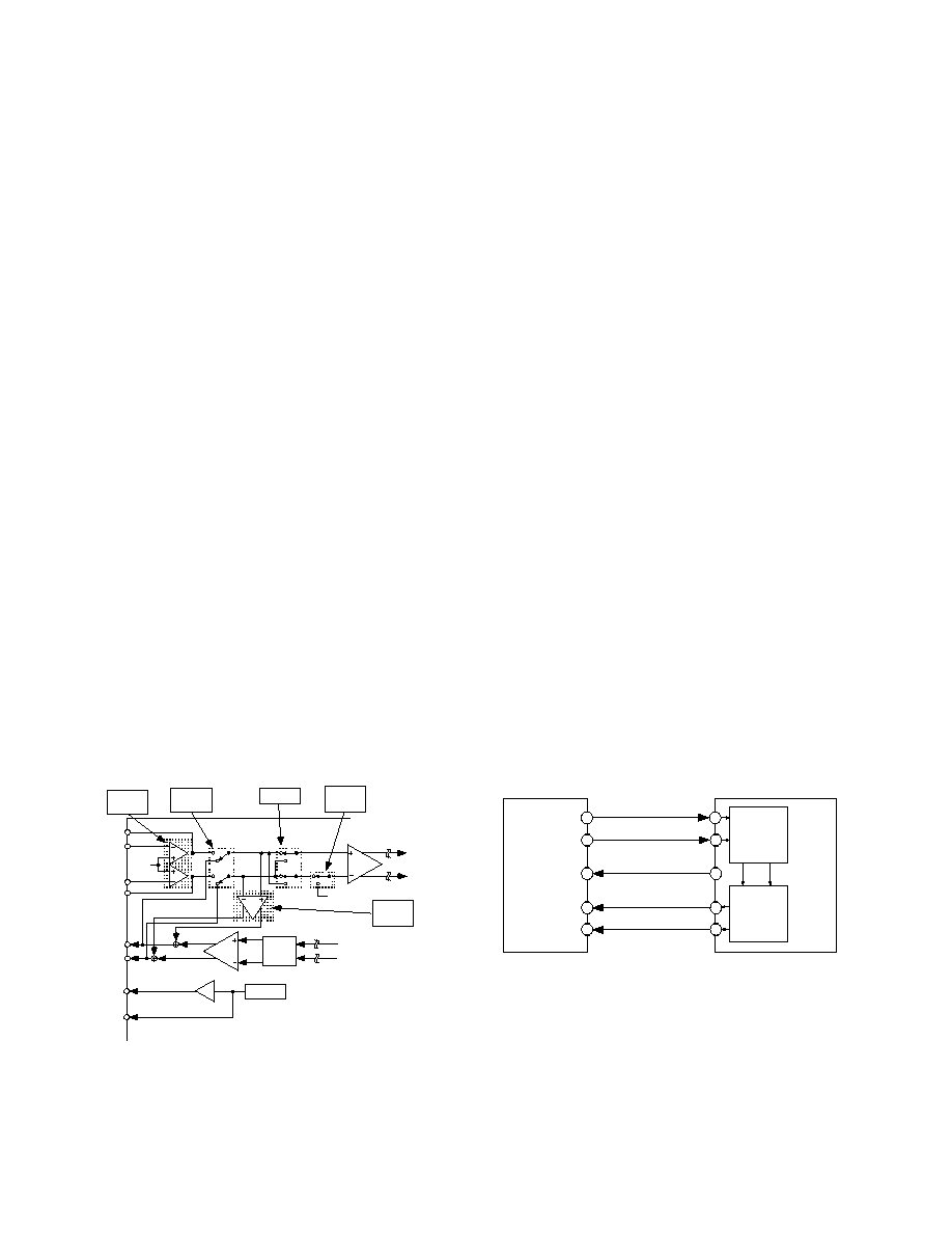
AD73522
�22�
REV. PrC 05/99
Preliminary Technical Data
PRELIMINAR
Y
TECHNICAL
DA
TA
the data. Note that the output samples from the ADC will
also have the MSB set to zero to indicate it is a data word.
A description of a single device operating in mixed mode is
detailed in Appendix B, while Appendix D details the initial-
ization and operation of a dual codec cascade operating in
mixed mode. Note that it is not essential to load the control
registers in Program Mode before setting mixed mode active.
It is also possible to initiate mixed mode by programming
CRA with the first control word and then interleaving control
words with DAC data.
Digital Loop-Back
This mode can be used for diagnostic purposes and allows the
user to feed the ADC samples from the ADC register directly
to the DAC register. This forms a loop-back of the analog
input to the analog output by reconstructing the encoded
signal using the decoder channel. The serial interface will
continue to work, which allows the user to control gain
settings, etc. Only when DLB is enabled with mixed mode
operation can the user disable the DLB, otherwise the device
must be reset.
SPORT Loop-Back
This mode allows the user to verify the DSP interfacing and
connection by writing words to the SPORT of the devices
and have them returned back unchanged after a delay of 16
SCLK cycles. The frame sync and data word that are sent to
the device are returned via the output port. Again, SLB mode
can only be disabled when used in conjunction with mixed
mode, otherwise the device must be reset.
Analog Loop-Back
In Analog Loop-Back mode, the differential DAC output is
connected, via a loopback switch, to the ADC input. This
mode allows the ADC channel to check functionality of the
DAC channel as the reconstructed output signal can be
monitored using the ADC as a sampler. Analog Loop-Back is
enabled by setting the ALB bit (CRF:7)
NOTE: Analog Loop-Back can only be enabled if the Analog
Gain Tap is powered-down (CRC:1 = 0).
Gain
+/- 1
VINN1
VINP1
VFBN1
VFBP1
V
REF
VOUTP1
VOUTN1
Continuous
Time
Low-Pass
Filter
+6/-15dB
PGA
V
REF
AD73422
AFE
SECTION
Analog
Loopback
Enabled
Single-Ended
Enable
Invert
Inverting Op-
amps
Analog Gain
Tap powered
Down
0/38 dB
PGA
REFOUT
REFCAP
Reference
Figure 9. Analog Loop-Back Connectivity
AFE INTERFACING
The AFE section SPORT (SPORT2) can be interfaced to
either SPORT0 or SPORT1 of the DSP section. Both serial
input and output data use an accompanying frame
synchronization signal which is active high one clock cycle
before the start of the 16-bit word or during the last bit of the
previous word if transmission is continuous. The serial clock
(SCLK) is an output from the codec and is used to define the
serial transfer rate to the DSP's Tx and Rx ports. Two primary
configurations can be used: the first is shown in Figure 10
where the DSP's Tx data, Tx frame sync, Rx data and Rx
frame sync are connected to the codec's SDI, SDIFS, SDO
and SDOFS respectively. This configuration, referred to as
indirectly coupled or non frame sync loop-back, has the effect
of decoupling the transmission of input data from the receipt
of output data. The delay between receipt of codec output
data and transmission of input data for the codec is
determined by the DSP's software latency. When
programming the DSP serial port for this con-
figuration, it is necessary to set the Rx FS as an input and the
Tx FS as an output generated by the DSP. This configuration
is most useful when operating in mixed mode, as the DSP has
the ability to decide how many words (either DAC or control)
can be sent to the codecs. This means that full control can be
implemented over the device configuration as well as updating
the DAC in a given sample interval. The second configura-
tion (shown in Figure 11) has the DSP's Tx data and Rx data
connected to the codec's SDI and SDO, respectively while
the DSP's Tx and Rx frame syncs are connected to the
codec's SDIFS and SDOFS. In this configuration, referred to
as directly coupled or frame sync loop-back, the frame sync
signals are connected together and the input data to the
codec is forced to be synchronous with the output data from
the codec. The DSP must be programmed so that both the
Tx FS and Rx FS are inputs as the codec SDOFS will be
input to both. This configuration guarantees that input and
output events occur simultaneously and is the simplest
configuration for operation in normal Data Mode. Note that
when programming the DSP in this configuration it is
advisable to preload the Tx register with the first control word
to be sent before the codec is taken out of reset. This ensures
that this word will be transmitted to coincide with the first
output word from the device(s).
AFE
SECTION
SDIFS
SDI
SCLK2
SDO
SDOFS
TFS(0/1)
DT(0/1)
SCLK(0/1)
DR(0/1)
RFS(0/1)
DSP
SECTION
CHANNEL 1
CHANNEL 2
AD73422
Figure 10. Indirectly Coupled or Non Frame Sync Loop-
Back Configuration
Cascade Operation
The AD73522 has been designed to support cascading of
extra external AFEs from either SPORT0 or SPORT1.
Cascaded operation can support mixes of dual or single
channel devices with maximum number of codec units being
eight (the AD73522 has two codec units configured on the
device). The SPORT2 interface protocol has been designed
so that device addressing is built into the packet of
information sent to the device. This allows the cascade to be
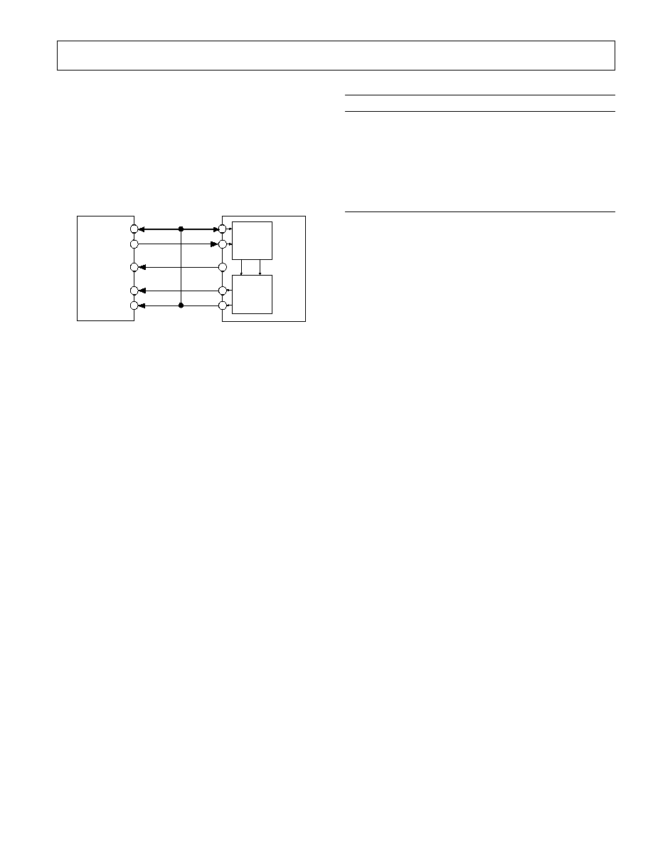
AD73522
�23�
REV. PrC 05/99
Preliminary Technical Data
PRELIMINAR
Y
TECHNICAL
DA
TA
formed with no extra hardware overhead for control signals or
addressing. A cascade can be formed in either of the two
modes previously discussed.
There may be some restrictions in cascade operation due to
the number of devices configured in the cascade and the
sampling rate and serial clock rate chosen.
The following
relationship details the restrictions in configuring a codec
cascade.
Number of Codecs * Word Size(16) * Sampling rate <=
Serial Clock Rate
AFE
SECTION
SDIFS
SDI
SCLK2
SDO
SDOFS
TFS(0/1)
DT(0/1)
SCLK(0/1)
DR(0/1)
RFS(0/1)
DSP
SECTION
CHANNEL 1
CHANNEL 2
AD73422
Figure 11. Directly Coupled or Frame Sync Loop-
Back Configuration
When using the indirectly coupled frame sync configuration
in cascaded operation it is necessary to be aware of the
restrictions in sending data to all devices in the cascade.
Effectively the time allowed is given by the sampling interval
(M/DMCLK - where M can be one of 256, 512, 1024 or
2048) which is 125 �s for a sample rate of 8 kHz. In this
interval, the DSP must transfer N
16 bits of information
where N is the number of devices in the cascade. Each bit will
take 1/SCLK and, allowing for any latency between the
receipt of the RX interrupt and the transmission of the TX
data, the relationship for successful operation is given by:
M/DMCLK > ((N/SCLK) + T
INTERRUPT LATENCY
)
The interrupt latency will include the time between the ADC
sampling event and the RX interrupt being generated in the
DSP--this should be 16 SCLK cycles.
As the AD73522 is configured in Cascade Mode, each
device must know the number of devices in the cascade
because the Data and Mixed modes use a method of counting
input frame sync pulses to decide when they should update
the DAC register from the serial input register. Control
Register A contains a 3-bit field (DC0�2) that is pro-
grammed by the DSP during the programming phase. The
default condition is that the field contains 000b, which is
equivalent to a single device in cascade (see Table XVIII).
However, for cascade operation this field must contain a
binary value that is one less than the number of devices in the
cascade, which is 001b for a single AD73522 device
configuration.
Table XVIII. Device Count Settings
DC2
DC1
DC0
Cascade Length
0
0
0
1
0
0
1
2
0
1
0
3
0
1
1
4
1
0
0
5
1
0
1
6
1
1
0
7
1
1
1
8
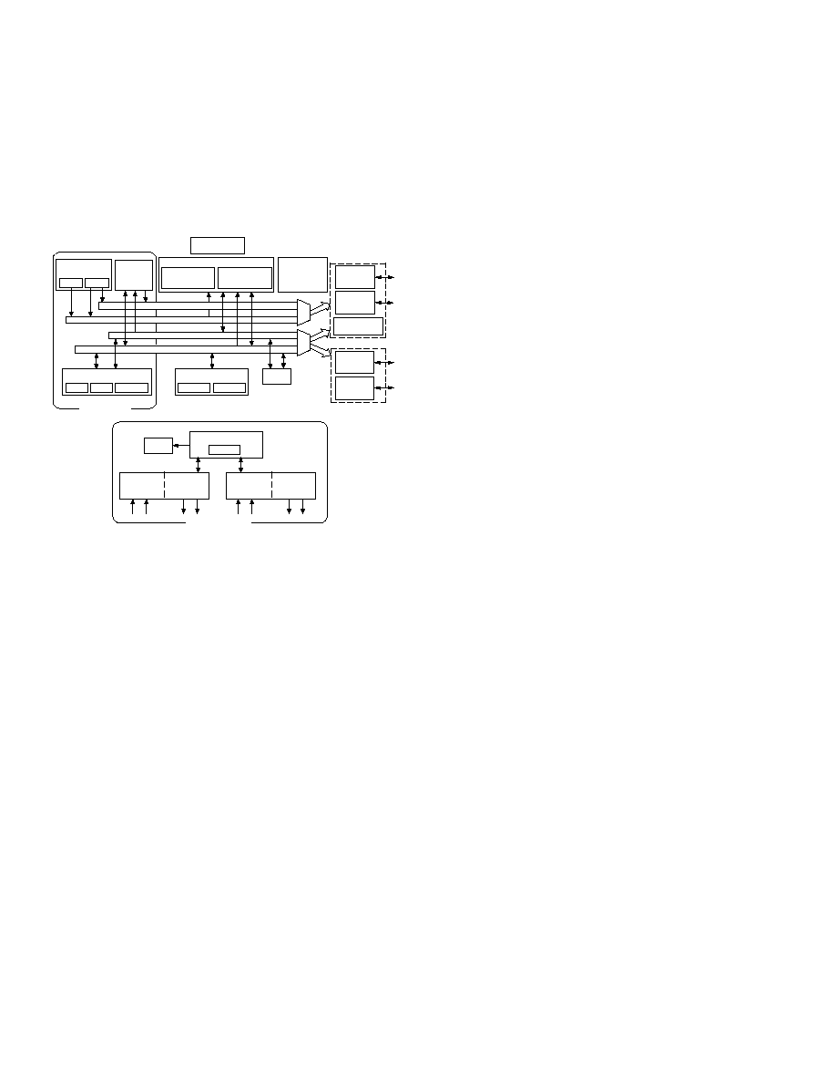
AD73522
�24�
REV. PrC 05/99
Preliminary Technical Data
PRELIMINAR
Y
TECHNICAL
DA
TA
FUNCTIONAL DESCRIPTION - DSP
The AD73522 instruction set provides flexible data moves
and multifunction (one or two data moves with a
computation) instructions. Every instruction can be executed
in a single processor cycle. The AD73522 assembly language
uses an algebraic syntax for ease of coding and readability. A
comprehensive set of development tools supports program
development.
SERIAL PORTS
SPORT 1
SPORT 0
MEMORY
PROGRAMMABLE
I/O
AND
FLAGS
BYTE DMA
CONTROLLER
16K PM
(OPTIONAL 8K)
TIMER
ADSP-2100 BASE
ARCHITECTURE
SHIFTER
MAC
ALU
ARITHMETIC UNITS
POWER-DOWN
CONTROL
PROGRAM
SEQUENCER
DAG 2
DAG 1
DATA ADDRESS
GENERATORS
PROGRAM MEMORY ADDRESS
DATA MEMORY ADDRESS
PROGRAM MEMORY DATA
DATA MEMORY DATA
EXTERNAL
DATA
BUS
EXTERNAL
ADDRESS
BUS
INTERNAL
DMA
PORT
EXTERNAL
DATA
BUS
OR
FULL MEMORY
MODE
HOST MODE
16K DM
(OPTIONAL 8K)
SERIAL PORT
REF
ADC1
ADC2
DAC1
DAC2
ANALOG FRONT END
SECTION
SPORT 2
Figure 12. Functional Block Diagram
Figure 12 is an overall block diagram of the AD73522. The
processor contains three independent computational units:
the ALU, the multiplier/accumulator (MAC) and the shifter.
The computational units process 16-bit data directly and have
provisions to support multiprecision computations. The ALU
performs a standard set of arithmetic and logic operations;
division primitives are also supported. The MAC performs
single-cycle multiply, multiply/add and multiply/subtract
operations with
40 bits of accumulation. The shifter performs logical and
arithmetic shifts, normalization, denormalization and derive
exponent operations.
The shifter can be used to efficiently implement numeric
format control including multiword and block floating-
point representations.
The internal result (R) bus connects the computational units
so that the output of any unit may be the input of any unit on
the next cycle.
A powerful program sequencer and two dedicated data address
generators ensure efficient delivery of operands to these compu-
tational units. The sequencer supports conditional jumps, sub-
routine calls and returns in a single cycle. With internal loop
counters and loop stacks, the AD73522 executes looped code
with zero overhead; no explicit jump instructions are required to
maintain loops.
Two data address generators (DAGs) provide addresses for
simultaneous dual operand fetches (from data memory and
program memory). Each DAG maintains and updates four
address pointers. Whenever the pointer is used to access data
(indirect addressing), it is post-modified by the value of one
of four possible modify registers. A length value may be
associated with each pointer to implement automatic modulo
addressing for
circular buffers.
Efficient data transfer is achieved with the use of five internal
buses:
� Program Memory Address (PMA) Bus
� Program Memory Data (PMD) Bus
� Data Memory Address (DMA) Bus
� Data Memory Data (DMD) Bus
� Result (R) Bus
The two address buses (PMA and DMA) share a single
external address bus, allowing memory to be expanded off-
chip, and the two data buses (PMD and DMD) share a single
external data bus. Byte memory space and I/O memory space
also share the external buses.
Program memory can store both instructions and data, per-
mitting the AD73522 to fetch two operands in a single
cycle,
one from program memory and one from data memory.
The AD73522 can fetch an operand from program memory
and the next instruction in the same cycle.
In lieu of the address and data bus for external memory con-
nection, the AD73522 may be configured for 16-bit Internal
DMA port (IDMA port) connection to external systems. The
IDMA port is made up of 16 data/address pins and five
control pins. The IDMA port provides transparent, direct
access to the DSPs on-chip program and data RAM.
An interface to low cost byte-wide memory is provided by the
Byte DMA port (BDMA port). The BDMA port is
bidirectional and can directly address up to four megabytes of
external RAM or ROM for off-chip storage of program
overlays or data tables.
The byte memory and I/O memory space interface supports slow
memories and I/O memory-mapped peripherals with program-
mable wait state generation. External devices can gain control of
external buses with bus request/grant signals (
BR, BGH, and
BG). One execution mode (Go Mode) allows the AD73522 to
continue running from on-chip memory. Normal execution
mode requires the processor to halt while buses are granted.
The AD73522 can respond to eleven interrupts. There can be
up to six external interrupts (one edge-sensitive, two level-
sensitive and three configurable) and seven internal interrupts
generated by the timer, the serial ports (SPORTs), the Byte
DMA port and the power-down circuitry. There is also a
master
RESET signal. The two serial ports provide a complete
synchronous serial interface with optional companding in
hardware and a wide variety of framed or frameless data transmit
and receive modes of operation.
Each port can generate an internal programmable serial clock
or accept an external serial clock.
The AD73522 provides up to 13 general-purpose flag pins.
The data input and output pins on SPORT1 can be
alternatively configured as an input flag and an output flag. In
addition, there are eight flags that are programmable as inputs
or outputs and three flags that are always outputs.
A programmable interval timer generates periodic interrupts.
A 16-bit count register (TCOUNT) is decremented every n
processor cycle, where n is a scaling value stored in an 8-bit

AD73522
�25�
REV. PrC 05/99
Preliminary Technical Data
PRELIMINAR
Y
TECHNICAL
DA
TA
register (TSCALE). When the value of the count register
reaches zero, an interrupt is generated and the count register
is reloaded from a 16-bit period register (TPERIOD).
Serial Ports
The AD73522 incorporates two complete synchronous serial
ports (SPORT0 and SPORT1) for serial communications and
multiprocessor communication.
Here is a brief list of the capabilities of the AD73522
SPORTs. For additional information on Serial Ports, refer to
the ADSP-2100 Family User's Manual, Third Edition.
� SPORTs are bidirectional and have a separate, double-
buffered transmit and receive section.
� SPORTs can use an external serial clock or generate their
own serial clock internally.
� SPORTs have independent framing for the receive and
transmit sections. Sections run in a frameless mode or with
frame synchronization signals internally or externally
generated. Frame sync signals are active high or inverted,
with either of two pulsewidths and timings.
� SPORTs support serial data word lengths from 3 to 16 bits
and provide optional A-law and �-law companding accord-
ing to CCITT recommendation G.711.
� SPORT receive and transmit sections can generate unique
interrupts on completing a data word transfer.
� SPORTs can receive and transmit an entire circular buffer
of data with only one overhead cycle per data word. An
interrupt is generated after a data buffer transfer.
� SPORT0 has a multichannel interface to selectively receive
and transmit a 24- or 32-word, time-division multiplexed,
serial bitstream.
� SPORT1 can be configured to have two external interrupts
(
IRQ0 and IRQ1) and the Flag In and Flag Out signals.
The internally generated serial clock may still be used in
this
configuration.
DSP SECTION PIN DESCRIPTIONS
The AD73522 will be available in a 119 ball PBGA package.
In order to maintain maximum functionality and reduce pack-
age size and pin count, some serial port, programmable flag,
interrupt and external bus pins have dual, multiplexed func-
tionality. The external bus pins are configured during
RE-
SET only, while serial port pins are software configurable
during program execution. Flag and interrupt functionality is
retained concurrently on multiplexed pins. In cases where pin
functionality is reconfigurable, the default state is shown in
plain text; alternate functionality is shown in italics. See Pin
Descriptions on Page 10.
Memory Interface Pins
The AD73522 processor can be used in one of two modes,
Full Memory Mode, which allows BDMA operation with full
external overlay memory and I/O capability, or Host Mode,
which allows IDMA operation with limited external
addressing capabilities. The operating mode is determined by
the state of the Mode C pin during RESET and cannot be
changed while the processor is running. See tables for Full
Memory Mode Pins and Host Mode Pins for descriptions.
Full Memory Mode Pins (Mode C = 0)
Pin
# of
Input/
Name(s) Pins
Output Function
A13:0
14
O
Address Output Pins for Program,
Data, Byte and I/O Spaces
D23:0
24
I/O
Data I/O Pins for Program, Data,
Byte and I/O Spaces (8 MSBs are
also used as Byte Memory
addresses)
Host Mode Pins (Mode C = 1)
Pin
# of
Input/
Name(s) Pins
Output Function
IAD15:0 16
I/O
IDMA Port Address/Data Bus
A0
1
O
Address Pin for External I/O, Pro-
gram, Data or Byte access
D23:8
16
I/O
Data I/O Pins for Program, Data
Byte and I/O spaces
IWR
1
I
IDMA Write Enable
IRD
1
I
IDMA Read Enable
IAL
1
I
IDMA Address Latch Pin
IS
1
I
IDMA Select
IACK
1
O
IDMA Port Acknowledge Configur-
able in Mode D; Open Source
In Host Mode, external peripheral addresses can be decoded using the A0,
CMS, PMS, DMS and IOMS signals
Terminating Unused Pin
The following table shows the recommendations for
terminating unused pins.
Pin Terminations
I/O
Hi-Z*
Pin
3-State
Reset
Caused
Unused
Name
(Z)
State
By
Configuration
XTAL
I
I
Float
CLKOUT
O
O
Float
A13:1 or
O (Z)
Hi-Z
BR, EBR Float
IAD12:0
I/O (Z)
Hi-Z
IS
Float
A0
O (Z)
Hi-Z
BR, EBR Float
D23:8
I/O (Z)
Hi-Z
BR, EBR Float
D7 or
I/O (Z)
Hi-Z
BR, EBR Float
IWR
I
I
High (Inactive)
D6 or
I/O (Z)
Hi-Z
BR, EBR Float
IRD
I
I
BR, EBR High (Inactive)
D5 or
I/O (Z)
Hi-Z
Float
IAL
I
I
Low (Inactive)
D4 or
I/O (Z)
Hi-Z
BR, EBR Float
IS
I
I
High (Inactive)
D3 or
I/O (Z)
Hi-Z
BR, EBR Float
IACK
Float
D2:0 or
I/O (Z)
Hi-Z
BR, EBR Float
IAD15:13
I/O (Z)
Hi-Z
IS
Float
PMS
O (Z)
O
BR, EBR Float
DMS
O (Z)
O
BR, EBR Float
BMS
O (Z)
O
BR, EBR Float
IOMS
O (Z)
O
BR, EBR Float
CMS
O (Z)
O
BR, EBR Float
RD
O (Z)
O
BR, EBR Float

AD73522
�26�
REV. PrC 05/99
Preliminary Technical Data
PRELIMINAR
Y
TECHNICAL
DA
TA
Pin Terminations (Continued)
I/O
Hi-Z*
Pin
3-State
Reset
Caused
Unused
Name
(Z)
State
By
Configuration
WR
O (Z)
O
BR, EBR Float
BR
I
I
High (Inactive)
BG
O (Z)
O
EE
Float
BGH
O
O
Float
IRQ2/PF7
I/O (Z)
I
Input = High (Inactive)
or Program as Output,
Set to 1, Let Float
IRQL1/PF6 I/O (Z)
I
Input = High (Inactive)
or Program as Output,
Set to 1, Let Float
IRQL0/PF5 I/O (Z)
I
Input = High (Inactive)
or Program as Output,
Set to 1, Let Float
IRQE/PF4
I/O (Z)
I
Input = High (Inactive)
or Program as Output,
Set to 1, Let Float
SCLK0
I/O
I
Input = High or Low,
Output = Float
RFS0
I/O
I
High or Low
DR0
I
I
High or Low
TFS0
I/O
O
High or Low
DT0
O
O
Float
SCLK1
I/O
I
Input = High or Low,
Output = Float
RFS1/RQ0
I/O
I
High or Low
DR1/FI
I
I
High or Low
TFS1/RQ1
I/O
O
High or Low
DT1/FO
O
O
Float
EE
I
I
EBR
I
I
EBG
O
O
ERESET
I
I
EMS
O
O
EINT
I
I
ECLK
I
I
ELIN
I
I
ELOUT
O
O
NOTES
*
*Hi-Z = High Impedance.
1. If the CLKOUT pin is not used, turn it OFF.
2. If the Interrupt/Programmable Flag pins are not used, there are two options:
Option 1: When these pins are configured as INPUTS at reset and function as
interrupts and input flag pins, pull the pins High (inactive).
Option 2: Program the unused pins as OUTPUTS, set them to 1, and let them
float.
3. All bidirectional pins have three-stated outputs. When the pins is configured as
an output, the output is Hi-Z (high impedance) when inactive.
4. CLKIN, RESET, and PF3:0 are not included in the table because these pins
must be used.
Interrupts
The interrupt controller allows the processor to respond to the
eleven possible interrupts and
RESET with minimum overhead.
The AD73522 provides four dedicated external interrupt
input pins,
IRQ2, IRQL0, IRQL1 and IRQE. In addition,
SPORT1 may be reconfigured for
IRQ0, IRQ1, FLAG_IN and
FLAG_OUT, for a total of six external interrupts. The
AD73522 also supports internal interrupts from the timer, the
byte DMA port, the two serial ports, software and the power-
down control circuit. The interrupt levels are internally
prioritized and individually maskable (except power down and
reset). The
IRQ2, IRQ0 and IRQ1 input pins can be pro-
grammed to be
either level- or edge-sensitive.
IRQL0 and IRQL1 are level-
sensitive and
IRQE is edge sensitive. The priorities and vector
addresses of all interrupts are shown in Table XIX.
Table XIX. Interrupt Priority and Interrupt Vector Ad-
dresses
Interrupt Vector
Source of Interrupt
Address (Hex)
RESET (or Power-Up with PUCR = 1) 0000 (Highest Priority)
Power-Down (Nonmaskable)
002C
IRQ2
0004
IRQL1
0008
IRQL0
000C
SPORT0 Transmit
0010
SPORT0 Receive
0014
IRQE
0018
BDMA Interrupt
001C
SPORT1 Transmit or IRQ1
0020
SPORT1 Receive or IRQ0
0024
Timer
0028 (Lowest Priority)
Interrupt routines can either be nested with higher priority
interrupts taking precedence or processed sequentially. Inter-
rupts can be masked or unmasked with the IMASK register.
Individual interrupt requests are logically ANDed with the
bits in IMASK; the highest priority unmasked interrupt is
then selected. The power-down interrupt is nonmaskable.
The AD73522 masks all interrupts for one instruction cycle
following the execution of an instruction that modifies the
IMASK register. This does not affect serial port auto-
buffering or DMA transfers.
The interrupt control register, ICNTL, controls interrupt
nesting and defines the
IRQ0, IRQ1 and IRQ2 external inter-
rupts to be either edge- or level-sensitive. The
IRQE pin is an
external edge-sensitive interrupt and can be forced and
cleared. The
IRQL0 and IRQL1 pins are external level-sensi-
tive interrupts.
The IFC register is a write-only register used to force and
clear interrupts. On-chip stacks preserve the processor status
and are automatically maintained during interrupt handling.
The stacks are twelve levels deep to allow interrupt, loop and
subroutine nesting. The following instructions allow global
enable or disable servicing of the interrupts (including power
down), regardless of the state of IMASK. Disabling the
interrupts does not affect serial port autobuffering or DMA.
ENA INTS;
DIS INTS;
When the processor is reset, interrupt servicing is enabled.
LOW POWER OPERATION
The AD73522 has three low power modes that significantly
reduce the power dissipation when the device operates under
standby conditions. These modes are:
� Power-Down
� Idle
� Slow Idle

AD73522
�27�
REV. PrC 05/99
Preliminary Technical Data
PRELIMINAR
Y
TECHNICAL
DA
TA
The CLKOUT pin may also be disabled to reduce external
power dissipation.
Power-Down
The AD73522 processor has a low power feature that lets the
processor enter a very low power dormant state through hard-
ware or software control. Here is a brief list of power-down
features. Refer to the ADSP-2100 Family User's Manual, Third
Edition, "System Interface" chapter, for detailed information
about the power-down feature.
� Quick recovery from power-down. The processor begins
executing instructions in as few as 400 CLKIN cycles.
� Support for an externally generated TTL or CMOS proces-
sor clock. The external clock can continue running during
power-down without affecting the 400 CLKIN cycle recov-
ery.
� Support for crystal operation includes disabling the oscilla-
tor to save power (the processor automatically waits 4096
CLKIN cycles for the crystal oscillator to start and stabi-
lize), and letting the oscillator run to allow 400 CLKIN
cycle start up.
� Power-down is initiated by either the power-down pin
(
PWD) or the software power-down force bit Interrupt
support allows an unlimited number of instructions to be
executed before optionally powering down. The power-
down interrupt also can be used as a non-maskable, edge-
sensitive interrupt.
� Context clear/save control allows the processor to continue
where it left off or start with a clean context when leaving
the power-down state.
� The
RESET pin also can be used to terminate power-
down.
� Power-down acknowledge pin indicates when the processor
has entered power-down.
Idle
When the AD73522 is in the Idle Mode, the processor waits
indefinitely in a low power state until an interrupt occurs.
When an unmasked interrupt occurs, it is serviced; execution
then continues with the instruction following the IDLE
instruction. In Idle Mode IDMA, BDMA and autobuffer cycle
steals still occur.
Slow Idle
The IDLE instruction on the AD73522 slows the processor's
internal clock signal, further reducing power consumption.
The reduced clock frequency, a programmable fraction of the
normal clock rate, is specified by a selectable divisor given in
the IDLE instruction. The format of the instruction is
IDLE (n);
where n = 16, 32, 64 or 128. This instruction keeps the pro-
cessor fully functional, but operating at the slower clock rate.
While it is in this state, the processor's other internal clock
signals, such as SCLK, CLKOUT and timer clock, are re-
duced by the same ratio. The default form of the instruction,
when no clock divisor is given, is the standard IDLE instruc-
tion.
When the IDLE (n) instruction is used, it effectively slows
down the processor's internal clock and thus its response time
to incoming interrupts. The one-cycle response time of the
standard idle state is increased by n, the clock divisor. When
an enabled interrupt is received, the AD73522 will remain in
the idle state for up to a maximum of n processor cycles (n =
16, 32, 64 or 128) before resuming normal operation.
When the IDLE (n) instruction is used in systems that have
an externally generated serial clock (SCLK), the serial clock
rate may be faster than the processor's reduced internal clock
rate. Under these conditions, interrupts must not be
generated at a faster rate than can be serviced, due to the
additional time the processor takes to come out of the idle
state (a maximum of n processor cycles).
SYSTEM INTERFACE
Figure 13 shows a typical basic system configuration with the
AD73522, two serial devices, a byte-wide EPROM, and
optional external program and data overlay memories (mode
selectable). Programmable wait state generation allows the
processor to connect easily to slow peripheral devices. The
AD73522 also provides four external interrupts and two serial
ports or six external interrupts and one serial port. Host
Memory Mode allows access to the full external data bus, but
limits addressing to a single address bit (A0) Additional
system peripherals can be added in this mode through the use
of external hardware to generate and latch address signals.
Clock Signals
The AD73522 can be clocked by either a crystal or a TTL-
compatible clock signal.
The CLKIN input cannot be halted, changed during
operation or operated below the specified frequency during
normal operation. The only exception is while the processor is
in the power-down state. For additional information, refer
to Chapter 9, ADSP-2100 Family User's Manual, Third Edition,
for detailed information on this power-down feature.
If an external clock is used, it should be a TTL-compatible
signal running at half the instruction rate. The signal is con-
nected to the processor's CLKIN input. When an external
clock is used, the XTAL input must be left unconnected.
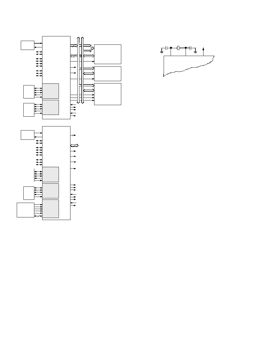
AD73522
�28�
REV. PrC 05/99
Preliminary Technical Data
PRELIMINAR
Y
TECHNICAL
DA
TA
1/2x CLOCK
OR
CRYSTAL
AFE*
SECTIONO
R
SERIAL
DEVICE
SCLK1
RFS1 OR
IRQ0
TFS1 OR
IRQ1
DT1 OR FO
DR1 OR FI
SPORT1
SCLK0
RFS0
TFS0
DT0
DR0
SPORT0
A0-A21
DATA
CS
BYTE
MEMORY
I/O SPACE
(PERIPHERALS)
CS
DATA
ADDR
DATA
ADDR
2048 LOCATIONS
OVERLAY
MEMORY
TWO 8K
PM SEGMENTS
TWO 8K
DM SEGMENTS
D
23-0
A
13-0
D
23-8
A
10-0
D
15-8
D
23-16
A
13-0
14
24
FL0-2
PF3
CLKIN
XTAL
ADDR13-0
DATA23-0
B M S
IOMS
P M S
D M S
C M S
B R
B G
B G H
P W D
P W D A C K
AD73422
1/2x CLOCK
OR
CRYSTAL
AFE*
SECTION
OR
SERIAL
DEVICE
SYSTEM
INTERFACE
OR
CONTROLLER
16
1
16
SPORT1
SCLK0
RFS0
TFS0
DT0
DR0
SPORT0
IAD15-0
IDMA PORT
FL0-2
PF3
CLKIN
XTAL
A0
DATA23-8
B M S
IOMS
P M S
D M S
C M S
B R
B G
B G H
P W D
P W D A C K
AD73422
IRQ2
/PF7
IRQE
/PF4
IRQL0
/PF5
IRQL1
/PF6
MODE C/PF2
MODE B/PF0
MODE A/PF1
HOST MEMORY MODE
IRQ2
/PF7
IRQE
/PF4
IRQL0
/PF5
IRQL1
/PF6
MODE C/PF2
MODE B/PF0
MODE A/PF1
FULL MEMORY MODE
IRD
/D6
IWR
/D7
IS
/D4
SCLK1
RFS1 OR
IRQ0
TFS1 OR
IRQ1
DT1 OR FO
DR1 OR FI
AFE*
SECTION
OR
SERIAL
DEVICE
IAL/D5
IACK
/D3
W R
R D
W R
R D
AFE*
SECTION
OR
SERIAL
DEVICE
*AFE SECTION CAN BE CONNECTED TO EITHER SPORT0 OR
SPORT1
Figure 13. AD73522 Basic System Configuration
The AD73522 uses an input clock with a frequency equal to
half the instruction rate; a 26.00 MHz input clock yields a 19
ns processor cycle (which is equivalent to 52 MHz).
Normally, instructions are executed in a single processor
cycle. All device timing is relative to the internal instruction
clock rate, which is indicated by the CLKOUT signal when
enabled.
Because the AD73522 includes an on-chip oscillator circuit,
an external crystal may be used. The crystal should be connected
across the CLKIN and XTAL pins, with two capacitors con-
nected as shown in Figure 14. Capacitor values are dependent
on crystal type and should be specified by the crystal manu-
facturer. A
parallel-resonant, fundamental frequency, microprocessor-
grade crystal should be used.
A clock output (CLKOUT) signal is generated by the proces-
sor at the processor's cycle rate. This can be enabled and
disabled by the CLK0DIS bit in the SPORT0 Autobuffer
Control Register.
CLKIN
CLKOUT
XTAL
DSP
Figure 14. External Crystal Connections
Reset
The
RESET signal initiates a master reset of the AD73522.
The
RESET signal must be asserted during the power-up
sequence to assure proper initialization.
RESET during initial
power-up must be held long enough to allow the internal
clock to stabilize. If
RESET is activated any time after power-
up, the clock continues to run and does not require
stabilization time.
The power-up sequence is defined as the total time required
for the crystal oscillator circuit to stabilize after a valid V
DD
is
applied to the processor, and for the internal phase-locked
loop (PLL) to lock onto the specific crystal frequency. A
minimum of 2000 CLKIN cycles ensures that the PLL has
locked, but does not include the crystal oscillator start-up
time. During this power-up sequence the
RESET signal
should be held low. On any subsequent resets, the
RESET
signal must meet the minimum pulsewidth specification, t
RSP
.
The
RESET input contains some hysteresis; however, if an
RC circuit is used to generate the
RESET signal, an external
Schmidt trigger is recommended.
The master reset sets all internal stack pointers to the empty
stack condition, masks all interrupts and clears the MSTAT
register. When
RESET is released, if there is no pending bus
request and the chip is configured for booting, the boot-
loading sequence is performed. The first instruction is
fetched from on-chip program memory location 0x0000
once boot loading completes.
MODES OF OPERATION
Table XX summarizes the AD73522 memory modes.
Setting Memory Mode
Memory Mode selection for the AD73522 is made during
chip reset through the use of the Mode C pin. This pin is
multiplexed with the DSP's PF2 pin, so care must be taken in
how the mode selection is made. The two methods for
selecting the value of Mode C are active and passive.
Passive configuration involves the use a pull-up or pull-
down
resistor connected to the Mode C pin. To minimize power
consumption, or if the PF2 pin is to be used as an output
in the DSP application, a weak pull-up or pull-down, on the
order of 100 k
, can be used. This value should be sufficient
to pull the pin to the desired level and still allow the pin to
operate as
a programmable flag output without undue strain on the
processor's output driver. For minimum power consumption
during power-down, reconfigure PF2 to be an input, as the
AD73522
�29�
REV. PrC 05/99
Preliminary Technical Data
PRELIMINAR
Y
TECHNICAL
DA
TA
pull-up or pull-down will hold the pin in a known state, and
will not switch.
Active configuration involves the use of a three-statable
external driver connected to the Mode C pin. A driver's
output enable should be connected to the DSP's RESET
signal such that it only drives the PF2 pin when RESET is
active (low). When RESET is deasserted, the driver should
three-state, thus allowing full use of the PF2 pin as either an
input or output. To minimize power consumption during
power-down, configure the programmable flag as an output
when connected to a three-stated buffer. This ensures that
the pin will be held at a constant level and not oscillate should
the three-state driver's level hover around the logic switching
point.
MEMORY ARCHITECTURE
The AD73522 provides a variety of memory and peripheral
interface options. The key functional groups are Program
Memory, Data Memory, Byte Memory, and I/O. Refer to the
following figures and tables for PM and DM memory alloca-
tions in the AD73522.
PROGRAM MEMORY
Program Memory (Full Memory Mode) is a 24-bit-wide
space for storing both instruction opcodes and data. The
AD73522-80 has 16K words of Program Memory RAM on
chip (the AD73522-40 has 8K words of Program Memory
RAM on chip), and the capability of accessing up to two 8K
external memory overlay spaces using the external data bus.
Program Memory (Host Mode) allows access to all internal
memory. External overlay access is limited by a single external
address line (A0). External program execution is not available
in host mode due to a restricted data bus that is 16-bits wide
only.
Table XXI. PMOVLAY Bits
PMOVLAY
Memory
A13
A12:0
0,
Internal
Not Applicable
Not Applicable
1
External
0
13 LSBs of Ad-
dress
Overlay 1
Between 0x2000
and 0x3FFF
2
External
1
13 LSBs of Ad-
dress
Overlay 2
Between 0x2000
and 0x3FFF
ACCESSIBLE WHEN
PMOVLAY = 2
ACCESSIBLE WHEN
PMOVLAY = 1
ALWAYS
ACCESSIBLE
AT ADDRESS
0
x
0000 > 0
x
1FFF
ACCESSIBLE WHEN
PMOVLAY = 03
PM (MODE B = 0)
INTERNAL
MEMORY
EXTERNAL
MEMORY
0
x2000>
0x3FFF
0
x2000>
0x3FFF
2
0
x2000>
0x3FFF
2
8K INTERNAL
PMOVLAY = 03
8K EXTERNAL
PROGRAM MEMORY
MODE B = 1
ADDRESS
0
x
3FFF
0
x
2000
0
x
1FFF
0
x
0000
8K INTERNAL
PMOVLAY = 03
OR
8K EXTERNAL
PMOVLAY = 1 OR 2
0
x
3FFF
0
x
2000
0
x
1FFF
8K INTERNAL
0
x
0000
PROGRAM MEMORY
MODE B = 0
ADDRESS
ACCESSIBLE WHEN
PMOVLAY = 0
INTERNAL
MEMORY
EXTERNAL
MEMORY
0
x2000>
0x3FFF
0
x0000>
0x1FFF
2
PM (MODE B = 1)
1
RESERVED
1
WHEN MODE B = 1, PMOVLAY MUST BE SET TO 0
2
SEE TABLE III FOR PMOVLAY BITS
3NOT ACCESSIBLE ON AD73422-40
ACCESSIBLE WHEN
PMOVLAY = 03
RESERVED
Figure 15. Program Memory Map
Table XXI. Modes of Operations
1
MODE C
2
MODE B
3
MODE A
4
Booting Method
0
0
0
BDMA feature is used to load the first 32 program memory words from the byte
memory space. Program execution is held off until all 32 words have been loaded.
Chip is configured in Full Memory Mode.
5
0
1
0
No Automatic boot operations occur. Program execution starts at external memory
location 0. Chip is configured in Full Memory Mode. BDMA can still be used, but the
processor does not automatically use or wait for these operations.
1
0
0
BDMA feature is used to load the first 32 program memory words from the byte
memory space. Program execution is held off until all 32 words have been loaded.
Chip is configured in Host Mode. (REQUIRES ADDITIONAL
HARDWARE.)
1
0
1
IDMA feature is used to load any internal memory as desired. Program execution
is held off until internal program memory location 0 is written to. Chip is
configured in Host Mode.
5
NOTES
1
All mode pins are recognized while RESET is active (low).
2
When Mode C = 0, Full Memory enabled. When Mode C = 1, Host Memory Mode enabled.
3
When Mode B = 0, Auto Booting enabled. When Mode B = 1, no Auto Booting.
4
When Mode A = 0, BDMA enabled. When Mode A = 1, IDMA enabled.
5
Considered as standard operating settings. Using these configurations allows for easier design and better memory management.
AD73522
�30�
REV. PrC 05/99
Preliminary Technical Data
PRELIMINAR
Y
TECHNICAL
DA
TA
DATA MEMORY
Data Memory (Full Memory Mode) is a 16-bit-wide space
used for the storage of data variables and for memory-mapped
control registers. The AD73522-80 has 16K words on Data
Memory RAM on chip (the AD73522-40 has 8K words on
Data Memory RAM on chip), consisting of 16,352 user-
accessible locations in the case of the AD73522-80 ( 8,160
user-accessible locations in the case of the AD73522-40) and
32 memory-mapped registers. Support also exists for up to
two 8K external memory overlay spaces through the external
data bus. All internal accesses complete in one cycle. Accesses
to external memory are timed using the wait states specified
by the DWAIT register.
ACCESSIBLE WHEN
DMOVLAY = 2
ACCESSIBLE WHEN
DMOVLAY = 1
32 MEMORY
MAPPED
REGISTERS
0
x
3FFF
0
x
2000
0
x
1FFF
INTERNAL
8160
WORDS
0
x
0000
DATA MEMORY
ADDRESS
ALWAYS
ACCESSIBLE
AT ADDRESS
0
x
2
000 > 0
x
3
FFF
ACCESSIBLE WHEN
DMOVLAY = 01
INTERNAL
MEMORY
EXTERNAL
MEMORY
0
x
0000>
0
x
1
1FFF
0
x
0000>
0
x
1FFF
0
x
0000>
0
x
1FFF
DATA MEMORY
8K INTERNAL
DMOVLAY = 01
OR
EXTERNAL 8K
DMOVLAY = 1, 2
0
x
3FE0
0
x
3FDF
1NOT ACCESSIBLE ON AD73422-40
Figure 16. Data Memory Map
Data Memory (Host Mode) allows access to all internal
memory. External overlay access is limited by a single external
address line (A0). The DMOVLAY bits are defined in Table
XXII.
Table XXII. DMOVLAY Bits
DMOVLAY
Memory
A13
A12:0
0,
Internal
Not Applicable
Not Applicable
1
External
0
13 LSBs of Ad-
dress
Overlay 1
Between 0x2000
and 0x3FFF
2
External
1
13 LSBs of Ad-
dress
Overlay 2
Between 0x2000
and 0x3FFF
I/O Space (Full Memory Mode)
The AD73522 supports an additional external memory space
called I/O space. This space is designed to support simple
connections to peripherals (such as data converters and
external registers) or to bus interface ASIC data registers. I/O
space supports 2048 locations of 16-bit wide data. The lower
eleven bits of the external address bus are used; the upper
three bits are undefined. Two instructions were added to the
core ADSP-2100 Family instruction set to read from and
write to I/O memory space. The I/O space also has four dedi-
cated 3-bit wait state registers, IOWAIT0-3, that specify up
to seven wait states to be automatically generated for each of
four regions. The wait states act on address ranges as shown
in Table XXIII.
Table XXIII. Wait States
Address Range
Wait State Register
0x000�0x1FF
IOWAIT0
0x200�0x3FF
IOWAIT1
0x400�0x5FF
IOWAIT2
0x600�0x7FF
IOWAIT3
Composite Memory Select (
CMS
CMS
CMS
CMS
CMS)
The AD73522 has a programmable memory select signal that
is useful for generating memory select signals for memories
mapped to more than one space. The
CMS signal is gener-
ated to have the same timing as each of the individual
memory select signals (
PMS, DMS, BMS, IOMS) but can
combine their
functionality.
Each bit in the CMSSEL register, when set, causes the
CMS
signal to be asserted when the selected memory select is as-
serted. For example, to use a 32K word memory to act as
both program and data memory, set the
PMS and DMS bits
in the CMSSEL register and use the
CMS pin to drive the
chip select of the memory; use either
DMS or PMS as the
additional
address bit.
The
CMS pin functions like the other memory select signals,
with the same timing and bus request logic. A 1 in the enable
bit causes the assertion of the
CMS signal at the same time as
the selected memory select signal. All enable bits default to 1
at reset, except the
BMS bit.
Boot Memory Select (
BMS
BMS
BMS
BMS
BMS) Disable
The AD73522 also lets you boot the processor from one
external memory space while using a different external
memory space for BDMA transfers during normal operation.
You can use the
CMS to select the first external memory
space for BDMA transfers and
BMS to select the second
external memory space for booting. The
BMS signal can be
disabled by setting Bit 3 of the System Control Register to 1.
The System Control Register is illustrated in Figure 17.
0
0
0
0
0
1
0
0
0
0
0
0
0
1
1
1
15 14 13 12 11 10 9
8
7
6
5
4
3
2
1
0
DM (0 3FFF)
SYSTEM CONTROL REGISTER
SPORT0 ENABLE
1 = ENABLED, 0 = DISABLED
SPORT1 ENABLE
1 = ENABLED, 0 = DISABLED
SPORT1 CONFIGURE
1 = SERIAL PORT
0 = F1, FO,
IRQ0
,
IRQ1
, SCLK
PWAIT
PROGRAM MEMORY
WAIT STATES
B M S
ENABLE
0 = ENABLED, 1 = DISABLED
Figure 17. System Control Register
Byte Memory
The byte memory space is a bidirectional, 8-bit-wide, external
memory space used to store programs and data. Byte memory
is accessed using the BDMA feature. The BDMA Control
Register is shown in Figure 18. The byte memory space con-
sists of 256 pages, each of which is 16K
8.
The byte memory space on the AD73522 supports read and
write operations as well as four different data formats. The
byte memory uses data bits 15:8 for data. The byte memory
uses data bits 23:16 and address bits 13:0 to create a 22-bit
address. This allows up to a 4 meg
8 (32 megabit) ROM or
AD73522
�31�
REV. PrC 05/99
Preliminary Technical Data
PRELIMINAR
Y
TECHNICAL
DA
TA
RAM to be used without glue logic. All byte memory accesses
are timed by the BMWAIT register.
Byte Memory DMA (BDMA, Full Memory Mode)
The Byte memory DMA controller allows loading and storing
of program instructions and data using the byte memory
space. The BDMA circuit is able to access the byte memory
space while the processor is operating normally, and steals
only one DSP cycle per 8-, 16- or 24-bit word transferred.
BDMA CONTROL
BMPAGE
BDMA
OVERLAY
BITS
BTYPE
BDIR
0 = LOAD FROM BM
1 = STORE TO BM
BCR
0 = RUN DURING BDMA
1 = HALT DURING BDMA
0
0
0
0
0
0
0
0
0
0
0
0
1
0
0
0
1
5
1
4
1
3
1
2
1
1
1
0
9
8
7
6
5
4
3
2
1
0
DM
(0 3FE3)
Figure 18. BDMA Control Register
The BDMA circuit supports four different data formats that
are selected by the BTYPE register field. The appropriate
number of 8-bit accesses are done from the byte memory
space to build the word size selected. Table XXIV shows the
data formats supported by the BDMA circuit.
Table XXIV. Data Formats
Internal
BTYPE
Memory Space
Word Size
Alignment
00
Program Memory
24
Full Word
01
Data Memory
16
Full Word
10
Data Memory
8
MSBs
11
Data Memory
8
LSBs
Unused bits in the 8-bit data memory formats are filled with
0s. The BIAD register field is used to specify the starting
address for the on-chip memory involved with the transfer.
The 14-bit BEAD register specifies the starting address for
the external byte memory space. The 8-bit BMPAGE register
specifies the starting page for the external byte memory space.
The BDIR register field selects the direction of the transfer.
Finally the 14-bit BWCOUNT register specifies the number
of DSP words to transfer and initiates the BDMA circuit
transfers.
BDMA accesses can cross page boundaries during sequential
addressing. A BDMA interrupt is generated on the
completion of the number of transfers specified by the
BWCOUNT
register.
The BWCOUNT register is updated after each transfer so it
can be used to check the status of the transfers. When it
reaches zero, the transfers have finished and a BDMA
interrupt is generated. The BMPAGE and BEAD registers
must not be accessed by the DSP during BDMA operations.
The source or destination of a BDMA transfer will always be
on-chip program or data memory.
When the BWCOUNT register is written with a nonzero
value, the BDMA circuit starts executing byte memory
accesses with wait states set by BMWAIT. These accesses
continue until the count reaches zero. When enough accesses
have occurred to create a destination word, it is transferred to
or from on-chip memory. The transfer takes one DSP cycle.
DSP accesses to external memory have priority over BDMA
byte memory accesses.
The BDMA Context Reset bit (BCR) controls whether or not
the processor is held off while the BDMA accesses are occur-
ring. Setting the BCR bit to 0 allows the processor to
continue operations. Setting the BCR bit to 1 causes the
processor to stop execution while the BDMA accesses are
occurring, to clear the context of the processor and start
execution at address 0 when the BDMA accesses have
completed.
The BDMA overlay bits specify the OVLAY memory blocks
to be accessed for internal memory.
Internal Memory DMA Port (IDMA Port; Host Memory
Mode)
The IDMA Port provides an efficient means of
communication between a host system and the AD73522.
The port is used to access the on-chip program memory and
data memory of the DSP with only one DSP cycle per word
overhead. The IDMA port cannot be used, however, to write
to the DSP's memory-mapped control registers. A typical
IDMA transfer process is described as follows:
1. Host starts IDMA transfer.
2. Host checks
IACK control line to see if the DSP is busy.
3. Host uses
IS and IAL control lines to latch either the
DMA starting address (IDMAA) or the PM/DM OVLAY
selection into the DSP's IDMA control registers.
If IAD[15] = 1, the value of IAD[7:0] represent the IDMA
overlay: IAD[14:8] must be set to 0.
If IAD[15] = 0, the value of IAD[13:0] represent the
starting address of internal memory to be accessed and
IAD[14] reflects PM or DM for access.
4. Host uses
IS and IRD (or IWR) to read (or write) DSP
internal memory (PM or DM).
5. Host checks IACK line to see if the DSP has completed
the previous IDMA operation.
6. Host ends IDMA transfer.
The IDMA port has a 16-bit multiplexed address and data
bus and supports 24-bit program memory. The IDMA port
is
completely asynchronous and can be written to while the
AD73522 is operating at full speed.
The DSP memory address is latched and then automatically
incremented after each IDMA transaction. An external device
can therefore access a block of sequentially addressed memory
by specifying only the starting address of the block. This in-
creases throughput as the address does not have to be sent for
each memory access.
IDMA Port access occurs in two phases. The first is the
IDMA Address Latch cycle. When the acknowledge is
asserted, a
14-bit address and 1-bit destination type can be driven onto
the bus by an external device. The address specifies an on-
chip memory location; the destination type specifies whether
it is a DM or PM access. The falling edge of the address latch
signal latches this value into the IDMAA register.
AD73522
�32�
REV. PrC 05/99
Preliminary Technical Data
PRELIMINAR
Y
TECHNICAL
DA
TA
Once the address is stored, data can either be read from or
written to the AD73522's on-chip memory. Asserting the
select line (
IS) and the appropriate read or write line (IRD
and
IWR respectively) signals the AD73522 that a particular
transaction is required. In either case, there is a one-
processor-cycle delay for synchronization. The memory access
consumes one additional processor cycle.
Once an access has occurred, the latched address is automati-
cally incremented and another access can occur.
Through the IDMAA register, the DSP can also specify the
starting address and data format for DMA operation.
Asserting the IDMA port select (
IS) and address latch enable
(IAL) directs the AD73522 to write the address onto the
IAD0�14 bus into the IDMA Control Register. If IAD[15]
is set to 0, IDMA latches the address. If IAD[15] is set to
1, IDMA latches OVLAY memory. The IDMA OVLAY and
address are stored in separate memory-mapped registers. The
IDMAA register, shown below, is memory mapped at address
DM (0x3FE0). Note that the latched address (IDMAA)
cannot be read back by the host. The IDMA OVLAY register
is memory mapped at address DM (0x3FE7). See Figure 19
for more information on IDMA and DMA memory maps.
IDMA CONTROL (U = UNDEFINED AT RESET)
DM(0 3FE0)
IDMAA
ADDRESS
IDMAD
DESTINATION MEMORY TYPE:
0 = PM
1 = DM
U U U U U U U U U U U U U U U
1
5
1
4
1
3
1
2
1
1
1
0
9 8 7 6 5 4 3 2 1 0
Figure 19. IDMA Control/OVLAY Registers
Bootstrap Loading (Booting)
The AD73522 has two mechanisms to allow automatic load-
ing of the internal program memory after reset. The method
for booting after reset is controlled by the Mode A, B and C
configuration bits.
When the mode pins specify BDMA booting, the AD73522
initiates a BDMA boot sequence when reset is released.
The BDMA interface is set up during reset to the following
defaults when BDMA booting is specified: the BDIR,
BMPAGE, BIAD and BEAD registers are set to 0, the
BTYPE register is set to 0 to specify program memory 24-
bit words, and the BWCOUNT register is set to 32. This
causes 32 words of on-chip program memory to be loaded
from byte memory. These 32 words are used to set up the
BDMA to load in the remaining program code. The BCR bit
is also set to 1, which causes program execution to be held off
until all 32 words are loaded into on-chip program memory.
Execution then begins at address 0.
The ADSP-2100 Family Development Software (Revision
5.02 and later) fully supports the BDMA booting feature and
can generate byte memory space compatible boot code.
The IDLE instruction can also be used to allow the processor
to hold off execution while booting continues through the
BDMA interface. For BDMA accesses while in Host Mode,
the addresses to boot memory must be constructed externally
to the AD73522. The only memory address bit provided by
the processor is A0.
IDMA Port Booting
The AD73522 can also boot programs through its Internal
DMA port. If Mode C = 1, Mode B = 0 and Mode A = 1, the
AD73522 boots from the IDMA port. IDMA feature can load
as much on-chip memory as desired. Program execution is
held off until on-chip program memory location 0 is written
to.
Bus Request and Bus Grant (Full Memory Mode)
The AD73522 can relinquish control of the data and address
buses to an external device. When the external device requires
access to memory, it asserts the bus request (BR) signal. If
the AD73522 is not performing an external memory access, it
responds to the active BR input in the following processor
cycle by:
� three-stating the data and address buses and the
PMS,
DMS, BMS, CMS, IOMS, RD, WR output drivers,
� asserting the bus grant (
BG) signal, and
� halting program execution.
If Go Mode is enabled, the AD73522 will not halt program
execution until it encounters an instruction that requires an
external memory access.
If the AD73522 is performing an external memory access
when the external device asserts the
BR signal, it will not
three-state the memory interfaces or assert the
BG signal until
the processor cycle after the access completes. The
instruction does not need to be completed when the bus is
granted. If a single instruction requires two external memory
accesses, the bus will be granted between the two accesses.
When the
BR signal is released, the processor releases the BG
signal, reenables the output drivers and continues program
execution from the point at which it stopped.
The bus request feature operates at all times, including when
the processor is booting and when
RESET is active.
The
BGH pin is asserted when the AD73522 is ready to ex-
ecute an instruction, but is stopped because the external bus
is already granted to another device. The other device can
release the bus by deasserting bus request. Once the bus is
released, the AD73522 deasserts
BG and BGH and executes
the external memory access.
Flag I/O Pins
The AD73522 has eight general purpose programmable
input/output flag pins. They are controlled by two memory
mapped registers. The PFTYPE register determines the direc-
tion, 1 = output and 0 = input. The PFDATA register is used
to read and write the values on the pins. Data being read from
a pin configured as an input is synchronized to the AD73522's
clock. Bits that are programmed as outputs will read the value
being output. The PF pins default to input during reset.
In addition to the programmable flags, the AD73522 has
five fixed-mode flags, FLAG_IN, FLAG_OUT, FL0, FL1
and FL2. FL0-FL2 are dedicated output flags. FLAG_IN
AD73522
�33�
REV. PrC 05/99
Preliminary Technical Data
PRELIMINAR
Y
TECHNICAL
DA
TA
and FLAG_OUT are available as an alternate configuration
of SPORT1.
Note: Pins PF0, PF1, PF2 and PF3 are also used for device
configuration during reset.
INSTRUCTION SET DESCRIPTION
The AD73522 assembly language instruction set has an
algebraic syntax that was designed for ease of coding and
readability. The assembly language, which takes full
advantage of the processor's unique architecture, offers the
following benefits:
� The algebraic syntax eliminates the need to remember
cryptic assembler mnemonics. For example, a typical
arithmetic add instruction, such as AR = AX0 + AY0,
resembles a simple equation.
� Every instruction assembles into a single, 24-bit word that
can execute in a single instruction cycle.
� The syntax is a superset ADSP-2100 Family assembly lan-
guage and is completely source and object code compatible
with other family members. Programs may need to be relo-
cated to utilize on-chip memory and conform to the
AD73522's interrupt vector and reset vector map.
� Sixteen condition codes are available. For conditional
jump, call, return or arithmetic instructions, the condition
can be checked and the operation executed in the same
instruction cycle.
� Multifunction instructions allow parallel execution of an
arithmetic instruction with up to two fetches or one write
to processor memory space during a single instruction
cycle.
DESIGNING AN EZ-ICE-COMPATIBLE SYSTEM
The AD73522 has on-chip emulation support and an ICE-
Port, a special set of pins that interface to the EZ-ICE. These
features allow in-circuit emulation without replacing the
target system processor by using only a 14-pin connection
from the target system to the EZ-ICE. Target systems must
have a 14-pin connector to accept the EZ-ICE's in-circuit
probe, a 14-pin plug. See the ADSP-2100 Family EZ-Tools data
sheet for complete information on ICE products.
Issuing the chip reset command during emulation causes the
DSP to perform a full chip reset, including a reset of its
memory mode. Therefore, it is vital that the mode pins are set
correctly PRIOR to issuing a chip reset command from the
emulator user interface. If you are using a passive method
of maintaining mode information (as discussed in Setting
Memory Modes) then it does not matter that the mode
information is latched by an emulator reset. However, if you
are using the
RESET pin as a method of setting the value of
the mode pins, then you have to take into consideration the
effects of an emulator reset.
One method of ensuring that the values located on the mode
pins are those desired is to construct a circuit like the one
shown in Figure 20. This circuit forces the value located on
the Mode A pin to logic high; regardless if it latched via the
RESET or ERESET pin.
ERESET
RESET
AD73422
MODE A/PFO
PROGRAMMABLE I/O
1k
Figure 20. Mode A Pin/EZ-ICE Circuit
The ICE-Port interface consists of the following AD73522 pins:
EBR
EBG
ERESET
EMS
EINT
ECLK
ELIN
ELOUT
EE
These AD73522 pins must be connected only to the EZ-ICE
connector in the target system. These pins have no function
except during emulation, and do not require pull-up or pull-
down resistors. The traces for these signals between the
AD73522 and the connector must be kept as short as pos-
sible, no longer than three inches.
The following pins are also used by the EZ-ICE:
BR
BG
RESET
GND
The EZ-ICE uses the EE (emulator enable) signal to take
control of the AD73522 in the target system. This causes the
processor to use its ERESET, EBR and EBG pins instead of
the RESET, BR and BG pins. The BG output is three-stated.
These signals do not need to be jumper-isolated in your
system.
The EZ-ICE
connects to your target system via a ribbon cable
and a 14-pin female plug. The ribbon cable is 10 inches in
length with one end fixed to the EZ-ICE. The female plug is
plugged onto the 14-pin connector (a pin strip header) on the
target board.
AD73522
�34�
REV. PrC 05/99
Preliminary Technical Data
PRELIMINAR
Y
TECHNICAL
DA
TA
Target Board Connector for EZ-ICE Probe
The EZ-ICE connector (a standard pin strip header) is shown
in Figure 21. You must add this connector to your target
board design if you intend to use the EZ-ICE. Be sure to
allow enough room in your system to fit the EZ-ICE probe
onto the 14-pin connector.
1
2
3
4
5
6
7
8
9
10
11
12
13
14
GND
KEY (NO PIN)
RESET
B R
B G
TOP VIEW
E B G
E B R
ELOUT
EE
EINT
ELIN
ECLK
E M S
ERESET
Figure 21. Target Board Connector for EZ-ICE
The 14-pin, 2-row pin strip header is keyed at the Pin 7 loca-
tion--you must remove Pin 7 from the header. The pins must
be 0.025 inch square and at least 0.20 inch in length. Pin
spacing should be 0.1 x 0.1 inches. The pin strip header must
have at least 0.15 inch clearance on all sides to accept the EZ-
ICE probe plug.
Pin strip headers are available from vendors such as 3M,
McKenzie and Samtec.
Target Memory Interface
For your target system to be compatible with the EZ-ICE
emulator, it must comply with the memory interface
guidelines listed below.
PM, DM, BM, IOM and CM
Design your Program Memory (PM), Data Memory (DM),
Byte Memory (BM), I/O Memory (IOM) and Composite
Memory (CM) external interfaces to comply with worst case
device timing requirements and switching characteristics as
specified in the DSP's data sheet. The performance of the
EZ-ICE
may approach published worst case specification for
some memory access timing requirements and switching
characteristics.
Note: If your target does not meet the worst case chip specifi-
cation for memory access parameters, you may not be able to
emulate your circuitry at the desired CLKIN frequency. De-
pending on the severity of the specification violation, you may
have trouble manufacturing your system as DSP components
statistically vary in switching characteristic and timing require-
ments within published limits.
Restriction: All memory strobe signals on the AD73522 (
RD,
WR, PMS, DMS, BMS, CMS and IOMS) used in your target
system must have 10 k
pull-up resistors connected when the
EZ-ICE is being used. The pull-up resistors are necessary
because there are no internal pull-ups to guarantee their state
during prolonged three-state conditions resulting from typical
EZ-ICE debugging sessions. These resistors may be removed
at your option when the EZ-ICE is not being used.
Target System Interface Signals
When the EZ-ICE
board is installed, the performance on
some system signals changes. Design your system to be com-
patible with the following system interface signal changes
introduced by the EZ-ICE
board:
� EZ-ICE
emulation introduces an 8 ns propagation delay
between your target circuitry and the DSP on the
RESET
signal.
� EZ-ICE
emulation introduces an 8 ns propagation delay
between your target circuitry and the DSP on the
BR
signal.
� EZ-ICE
emulation ignores RESET and BR when single-
stepping.
� EZ-ICE
emulation ignores
RESET and BR when in Emula-
tor Space (DSP halted).
� EZ-ICE
emulation ignores the state of target
BR in certain
modes. As a result, the target system may take control of
the DSP's external memory bus only if bus grant (BG) is
asserted by the EZ-ICE
board's DSP.
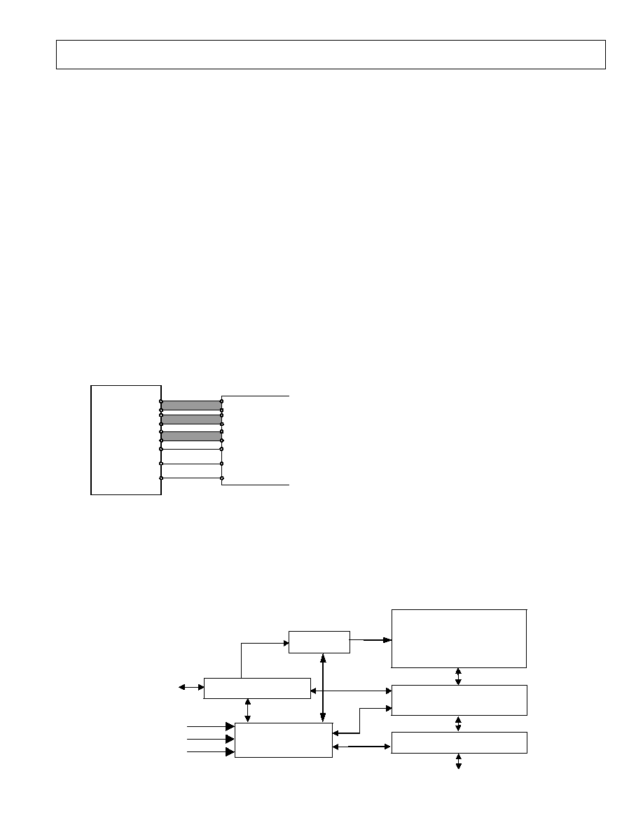
AD73522
�35�
REV. PrC 05/99
Preliminary Technical Data
PRELIMINAR
Y
TECHNICAL
DA
TA
FLASH MEMORY DESCRIPTION
The AD73522 features a 64K x 8 CMOS page mode
EEPROM which can be written with a 3.0-volt-only power
supply. Internal erase/program is transparent to the user.
Featuring high performance page write, the AD73522's flash
memory provides a typical byte-write time of 39 �sec. The
entire memory, i.e., 64K bytes, can be written page by page in
as little as 2.5 seconds, when using interface features such as
Toggle Bit or Data Polling to indicate the completion of a
write cycle. To protect against inadvertent write, the
AD73522 has on-chip hardware and software data protection
schemes.
The AD73522's flash memory has a guaranteed page-write
endurance of 10
4
or 10
3
cycles. Data retention is rated at
greater than 100 years. The AD73522 is suited for
applications that require convenient and economical updating
of program, configuration, or data memory.
Flash Memory Connection
The flash memory section of the AD73522 is configured on
the byte-wide DMA bus (BDMA) of the DSP section as
shown in Figure 22. Hence if boot operation is required from
the AD73522's internal flash memory, the boot mode
selection pins Mode A, Mode B and Mode C should be set to
zero (0).
DATA [0-7]
CE
BYTE
MEMORY
-FLASH
64 kbytes
D
15
D
17
A
13
B M S
AD73522
W R
R D
D
8
A
0
D
16
ADDRESS [0-13]
ADDRESS [14-15]
DB
7
DB
0
A
13
A
0
A
15
A
14
OE
W E
DSP
SECTION
Figure 22. Flash Interface to DSP section
Device Operation
The AD73522's page mode EEPROM offers in-circuit
electrical write capability. The AD73522 does not require
separate erase and program operations. The internally timed
write cycle executes both erase and program transparently to
the user. The AD73522 has industry standard optional
Software Data Protection, which is recommended to be
always enabled.
Read
The read operation of the AD73522 is controlled by
BMS
and
RD, both have to be low for the DSP section to obtain
data from the flash section.
BMS is used for device selection.
When
BMS is high, the flash memory is deselected and only
standby power is consumed.
RD is the output control and is
used to gate data from the flash output pins. The data bus is
in high impedance state when either
BMS or RD is high.
Refer to the read cycle timing diagram (Figure 24) for further
details.
Write
The write operation consists of three steps. The first step is
the optional three byte load sequence for Software Data
Protection. This is an optional first step in the write
operation, but highly recommended to ensure proper data
integrity. Step 2 is the byte-load cycle to a page buffer of the
flash. Step 3 is an internally controlled write cycle for writing
the data loaded in the page buffer into the memory array for
nonvolatile storage. During the byte-load cycle, the addresses
are latched by the falling edge of either
BMS or WR,
whichever occurs last. The data is latched by the rising edge
of either
BMS or WR, whichever occurs first. The internal
write cycle is initiated by a timer after the rising edge of
WR
or
BMS, whichever occurs first. The write cycle, once
initiated, will continue to completion, typically within 5 ms.
See Figures 25 and 26 for
WR and BMS controlled page
write cycle timing diagrams.
The write operation has three functional cycles: the optional
Software Data Protection load sequence, the page load cycle
and the internal write cycle. The Software Data Protection
consists of a specific three byte load sequence that will leave
the AD73522 protected at the end of the page write. The
page load cycle consists of loading 1 to 128 bytes of data into
the page buffer. The internal write cycle consists of the
TBLCO timeout and the write timer operation. During the
write operation, the only valid reads are Data Polling and
Toggle Bit. The page-write operation allows the loading of up
to 128 bytes of data into the page buffer of the AD73522
flash before the initiation of the internal write cycle. During
the internal write cycle, all the data in the page buffer is
written simultaneously into the memory array. Hence, the
Control Logic
A
15
- A
0
CE (BMS)
OE (RD)
WE (WR)
DB7 - DB0
524288 Bit
EEPROM
Cell Array
Y- Decoder and Page Latches
I/O Buffers and Data Latches
Address Buffer & Latches
X- Decoder
Figure 23. Flash Memory Organisation

AD73522
�36�
REV. PrC 05/99
Preliminary Technical Data
PRELIMINAR
Y
TECHNICAL
DA
TA
page-write feature of AD73522 allows the entire memory to
be written in as little as 2.5 seconds. During the internal write
cycle, the host is free to perform additional tasks, such as to
fetch data from other locations in the system to set up the
write to the next page. In each page-write operation, all the
bytes that are loaded into the page buffer must have the same
page address, i.e., A7 through A15. Any byte not loaded with
user data will be written to FF. See Figures 25 and 26 for the
page-write cycle timing diagrams. If after the initial byte-load
cycle, the host loads a second byte into the page buffer within
a byte-load cycle time (TBLC) of 100 �s, the AD73522 will
stay in the page load cycle. Additional bytes are then loaded
consecutively. The page load cycle will be terminated if no
additional byte is loaded into the page buffer within 200 �s
(TBLCO) from the last byte-load cycle, i.e., no subsequent
WR or BMS high-to-low transition after the last rising edge of
WR or BMS. Data in the page buffer can be changed by a
subsequent byte-load cycle. The page load period can
continue indefinitely, as long as the host continues to load the
device within the byte-load cycle time of 100 �s. The page to
be loaded is determined by the page address of the last byte
loaded.
Software Chip-Erase
The AD73522 provides a flash-erase operation, which allows
the user to simultaneously clear the entire flash-memory array
to the "1" state. This is useful when the entire flash memory
must be quickly erased. The Software Flash-Erase operation
is initiated by using a specific six byte-load sequence. After
the load sequence, the device enters into an internally timed
cycle similar to the write cycle. During the erase operation,
the only valid read is Toggle Bit. See Figure 30 for timing
diagram.
Write Operation Status Detection
The AD73522 provides two software means to detect the
completion of a write cycle, in order to optimize the system
write cycle time. The software detection includes two status
bits: Data Polling (DQ7) and Toggle Bit (DQ6). The end of
write detection mode is enabled after the rising WE or CE
whichever occurs first, which initiates the internal write cycle.
The actual completion of the nonvolatile write is
asynchronous with the system; therefore, either a Data Polling
or Toggle Bit read may be simultaneous with the completion
of the write cycle. If this occurs, the system may possibly get
an erroneous result, i.e., valid data may appear to conflict
with either DQ7 or DQ6. In order to prevent spurious
rejection, if an erroneous result occurs, the software routine
should include a loop to read the accessed location an
additional two (2) times. If both reads are valid, then the
device has completed the write cycle, otherwise the rejection
is valid.
Data Polling (DQ7)
When the AD73522 is in the internal write cycle, any attempt
to read DQ7 of the last byte loaded during the byte-load cycle
will receive the complement of the true data. Once the write
cycle is completed, DQ7 will show true data. The device is
then ready for the next operation. See Figure 27 for Data
Polling timing diagram.
Toggle Bit (DQ6)
During the internal write cycle, any consecutive attempts to
read DQ6 will produce alternating 0's and 1's, i.e., toggling
between 0 and 1. When the write cycle is completed, the
toggling will stop. The device is then ready for the next
operation. See Figure 28 for Toggle Bit timing diagram. The
initial read of the Toggle Bit will be a "1".
Data Protection
The AD73522 provides both hardware and software features
to protect nonvolatile data from inadvertent writes.
Hardware Data Protection
Noise/Glitch Protection: A
WR or BMS pulse of less than 5
ns will not initiate a write cycle. VDD Power Up/Down
Detection: The write operation is inhibited when VDD is less
than 2.5V.
Write Inhibit Mode: Forcing
RD low, BMS high, or WR high
will inhibit the write operation. This prevents inadvertent
writes during power-up or power-down.
Software Data Protection (SDP)
The AD73522 flash-memory provides the JEDEC approved
optional software data protection scheme for all data
alteration operations, i.e., write and chip erase. With this
scheme, any write operation requires the inclusion of a series
of three byte-load operations to precede the data loading
operation. The three byte-load sequence is used to initiate the
write cycle, providing optimal protection from inadvertent
write operations, e.g., during the system power-up or power-
down. The AD73522 is shipped with the software data
protection disabled. The software protection scheme can be
enabled by applying a three-byte sequence to the device,
during a page-load cycle (Figures 25 and 26). The device will
then be automatically set into the data protect mode. Any
subsequent write operation will require the preceding three-
byte sequence. See Figures 25 and 26 for the timing
diagrams. To set the device into the unprotected mode, a six-
byte sequence is required. See Figure 29 for the timing
diagram. If a write is attempted while SDP is enabled the
device will be in a non-accessible state for ~ 300 �s. It is
recommended that Software Data Protection always be
enabled.
The AD73522 Software Data Protection is a global
command, protecting (or unprotecting) all pages in the entire
memory array once enabled (or disabled). Therefore using
SDP for a single page write will enable SDP for the entire
array. Single pages by themselves cannot be SDP enabled or
disabled. Single power supply reprogrammable nonvolatile
memories may be unintentionally altered. SST strongly
recommends that Software Data Protection (SDP) always be
enabled. The AD73522 should be programmed using the
SDP command sequence. It is recommended that the SDP
Disable Command Sequence not be issued to the device prior
to writing.
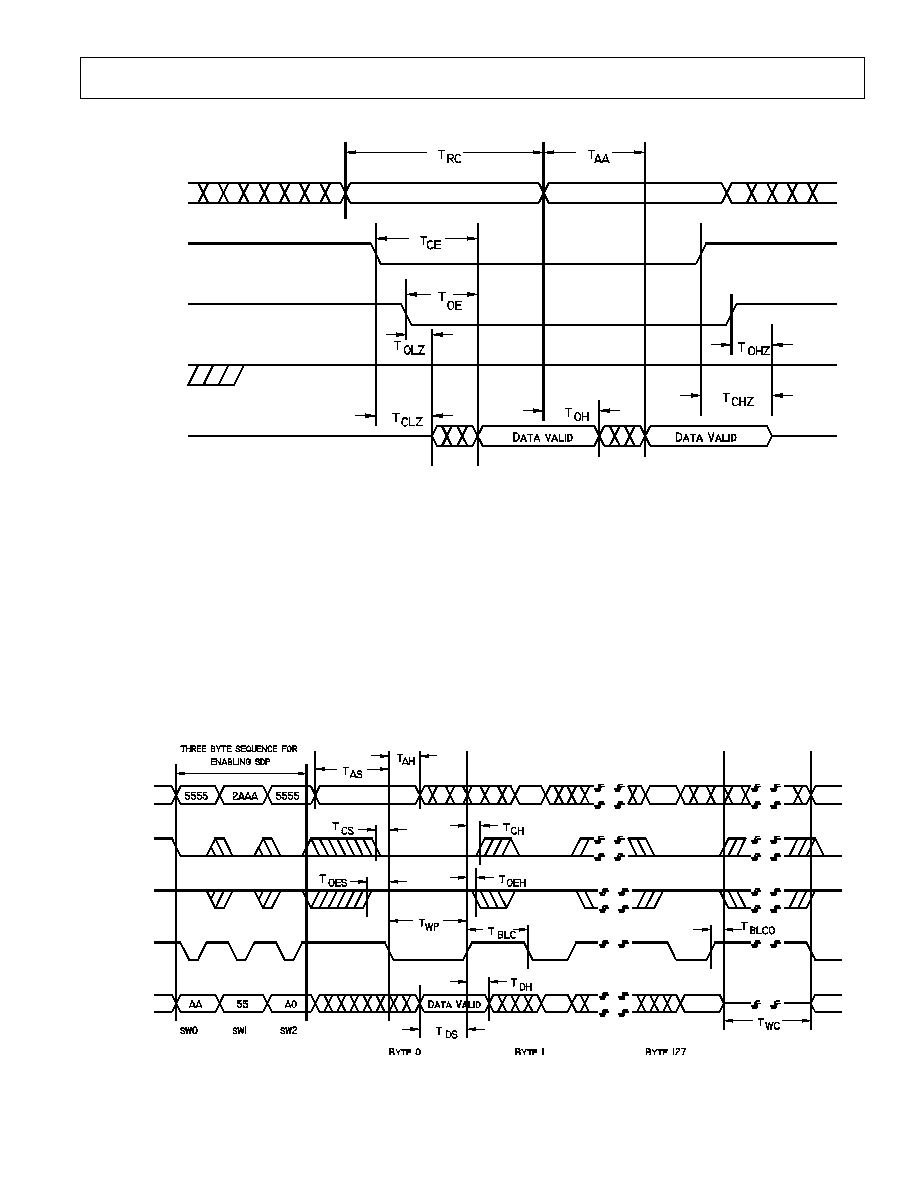
AD73522
�37�
REV. PrC 05/99
Preliminary Technical Data
PRELIMINAR
Y
TECHNICAL
DA
TA
ADDRESS A
15-0
CE (BMS)
WE (WR)
OE (RD)
DB
7-0
High-Z
V
IH
ADDRESS A
15-0
CE (BMS)
WE (WR)
OE (RD)
DB
7-0
Figure 24. Read Cycle Timing
Figure 25.
WR Controlled Page Mode Write Cycle Timing
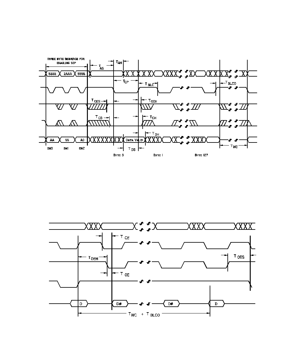
AD73522
�38�
REV. PrC 05/99
Preliminary Technical Data
PRELIMINAR
Y
TECHNICAL
DA
TA
ADDRESS A
15-0
CE (BMS)
WE (WR)
OE (RD)
DB
7-0
Figure 26.
BMS Controlled Page Mode Write Cycle
Timing
ADDRESS A
15-0
CE (BMS)
WE (WR)
OE (RD)
DB
7-0
Figure 27.
Data\ Polling Timing
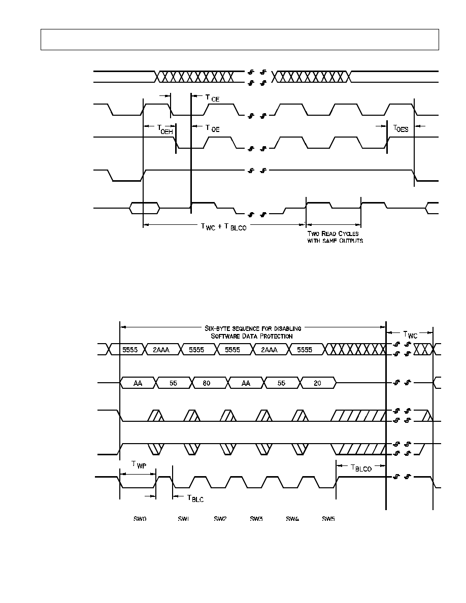
AD73522
�39�
REV. PrC 05/99
Preliminary Technical Data
PRELIMINAR
Y
TECHNICAL
DA
TA
ADDRESS A
15-0
CE (BMS)
WE (WR)
OE (RD)
DB
7-0
Figure 28.
Toggle Bit Timing
ADDRESS A
15-0
CE (BMS)
WE (WR)
OE (RD)
DB
7-0
Figure 29.
Software Data Protection Disable Timing
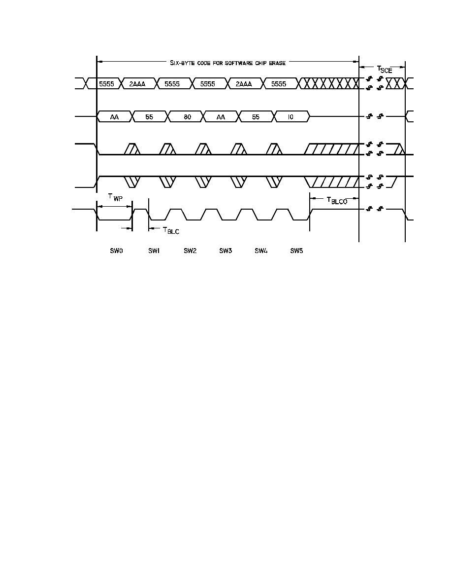
AD73522
�40�
REV. PrC 05/99
Preliminary Technical Data
PRELIMINAR
Y
TECHNICAL
DA
TA
Figure 30.
Software Flash-Memory Erase Timing
ADDRESS A
15-0
CE (BMS)
WE (WR)
OE (RD)
DB
7-0
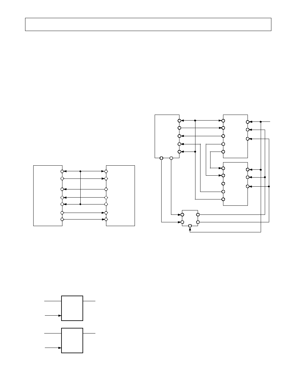
AD73522
�41�
REV. PrC 05/99
Preliminary Technical Data
PRELIMINAR
Y
TECHNICAL
DA
TA
ANALOG FRONT END (AFE) INTERFACING
The AFE section of the AD73522 features two voiceband
input/output channels, each with 16-bit linear resolution.
Connectivity to the AFE section from the DSP is
uncommitted thus allowing the user the flexibility of
connecting in the mode or configuration of their choice. This
section will detail several configurations - with no extra AFE
channels configured and with two extra AFE channels
configured (using an external AD73322 dual AFE).
DSP SPORT to AFE Interfacing
The SCLK, SDO, SDOFS, SDI and SDIFS pins of
SPORT2 must be connected to the Serial Clock, Receive
Data, Receive Data Frame Sync, Transmit Data and
Transmit Data Frame Sync pins respectively of either
SPORT0 or SPORT1.. The SE pin may be controlled from a
parallel output pin or flag pin such as FL0-2 or, where
SPORT2 powerdown is not required, it can be permanently
strapped high using a suitable pull-up resistor. The RESETC
pin may be connected to the system hardware reset structure
or it may also be controlled using a dedicated control line. In
the event of tying it to the global system reset, it is advisable
to operate the device in mixed mode, which allows a
software reset, otherwise there is no convenient way of
resetting the AFE section.
TFS
DT
SCLK
DR
RFS
DSP
SECTION
AFE
SECTION
SDIFS
SDI
SCLK
SDO
SDOFS
FL0
FL1
RESETC
SE
Figure 21. AD73522 AFE to DSP Connection
Cascade Operation
Where it is required to configure extra analog I/O channels to
the existing two channels on the AD73522, it is possible to
cascade up to 6 more channels (using single channel
AD73311 or dual channel AD73322 AFEs) by using the
scheme described in Figure 23. It is necessary however to
ensure that the timing of the SE and RESET signals is syn-
chronized at each device in the cascade. A simple D type flip
flop is sufficient to sync each signal to the master clock
MCLK, as in Figure 22.
1/2
74HC74
CLK
D
Q
DSP CONTROL
TO SE
MCLK
SE SIGNAL SYNCHRONIZED
TO MCLK
1/2
74HC74
CLK
D
Q
DSP CONTROL
TO
RESET
MCLK
RESET
SIGNAL SYNCHRONIZED
TO MCLK
Figure 22. SE and
RESET Sync Circuit for Cascaded
Operation
Connection of a cascade of devices to a DSP, as shown in
Figure 23, is no more complicated than connecting a single
device. Instead of connecting the SDO and SDOFS to the
DSP's Rx port, these are now daisy-chained to the SDI and
SDIFS of the next device in the cascade. The SDO and
SDOFS of the final device in the cascade are connected to
the DSP section's Rx port to complete the cascade. SE and
RESET on all devices are fed from the signals that were
synchronized with the MCLK using the circuit as described
above. The SCLK from only one device need be connected
to the DSP section's SCLK input(s) as all devices will be
running at the same SCLK frequency and phase.
TFS
DT
DR
RFS
AFE
SECTION
SDIFS
SDI
SCLK
SDO
SDOFS
SCLK
DEVICE 1
MCLK
SE
RESET
ADDITIONAL
AD73322
CODEC
SDIFS
SDI
SCLK
SDO
SDOFS
DEVICE 2
MCLK
SE
RESET
74HC74
Q1
Q2
D1
D2
FL0
FL1
DSP
SECTION
Figure 23. Connection of an AD73322 Cascaded to
AD73522
Interfacing to the AFE's analog inputs and outputs
The AFE section of the AD73522 offers a flexible interface
for microphone pickups, line level signals or PSTN line
intefaces. This section will detail some of the configurations
that can be used with the input and output sections.
The AD73322 features both differential inputs and outputs
on each channel to provide optimal performance and avoid
common mode noise. It is also possible to interface either
inputs or outputs in single-ended mode. This section details
the choice of input and output configurations and also gives
some tips towards successful configuration of the analog
interface sections.
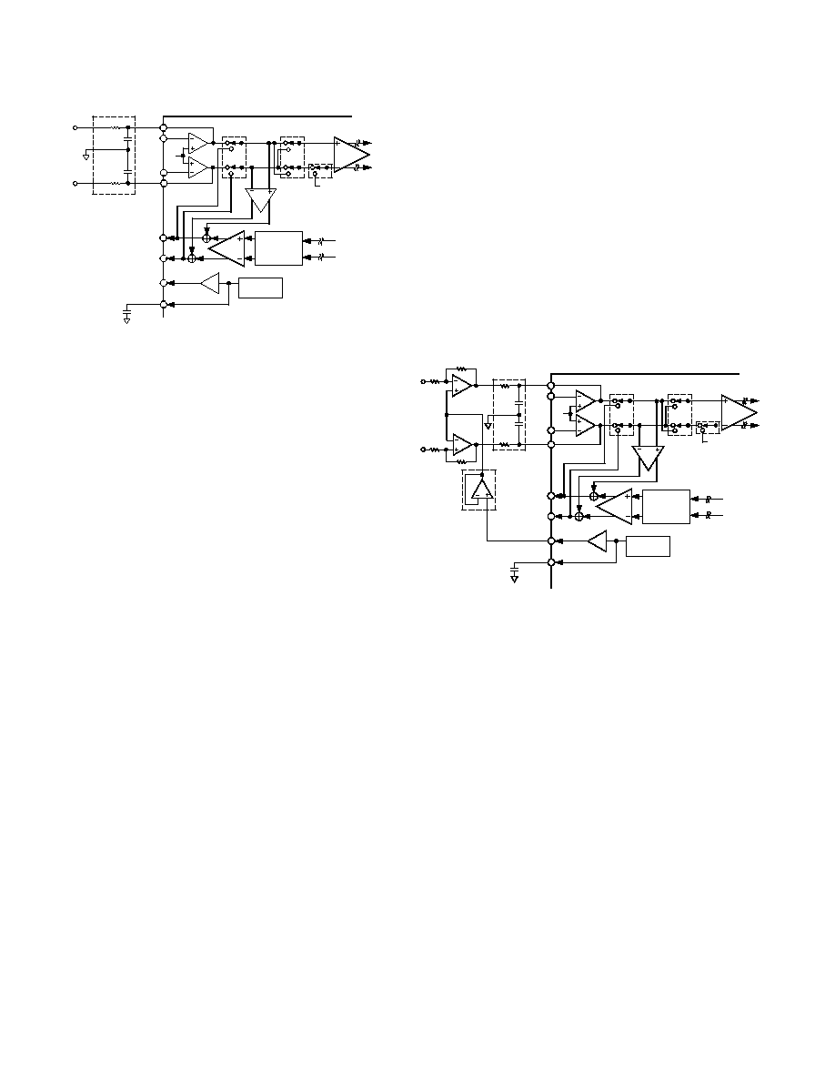
AD73522
�42�
REV. PrC 05/99
Preliminary Technical Data
PRELIMINAR
Y
TECHNICAL
DA
TA
VFBN1
GAIN
1
+6/15dB
PGA
CONTINUOUS
TIME
LOW-PASS
FILTER
V
REF
VINN
1
VINP1
VFBP1
VOUTP1
VOUTN1
REFOUT
REFERENCE
V
REF
ANTI-ALIAS
FILTER
0.047 F
100
0.047 F
100
REFCAP
0.1 F
0/38dB
PGA
Figure 24. Analog Input (DC-Coupled)
Analog Inputs
There are several different ways in which the analog input
(encoder) section of the AD73522 can be interfaced to
external circuitry. It provides optional input amplifiers which
allows sources with high source impedance to drive the ADC
section correctly. When the input amplifiers are enabled, the
input channel is configured as a differential pair of inverting
amplifiers referenced to the internal reference (REFCAP)
level. The inverting terminals of the input amplifier pair are
designated as pins VINP1 and VINN1 for Channel 1 (VINP2
and VINN2 for Channel 2) and the amplifier feedback
connections are available on pins VFBP1 and VFBN1 for
Channel 1 (VFBP2 and VFBN2 for Channel 2).
For applications where external signal buffering is required,
the input amplifiers can be bypassed and the ADC driven
directly. When the input amplifiers are disabled, the sigma-
delta modulator's input section (SC PGA) is accessed
directly through the VFBP1 and VFBN1 pins for Channel
1 (VFBP2 and VFBN2 for Channel 2).
It is also possible to drive the ADCs in either differential or
single-ended modes. If the single-ended mode is chosen it is
possible using software control to multiplex between two
single-ended inputs connected to the positive and negative
input pins.
The primary concerns in interfacing to the ADC are firstly to
provide adequate anti-alias filtering and to ensure that the
signal source will drive the switched-capacitor input of the
ADC correctly. The sigma-delta design of the ADC and its
over sampling characteristics simplify the antialias
requirements but it must be remembered that the single pole
RC filter is primarily intended to eliminate aliasing of
frequencies above the Nyquist frequency of the sigma-delta
modulator's sampling rate (typically 2.048 MHz). It may
still require a more specific digital filter implementation in the
DSP to provide the final signal frequency response
characteristics. It is recommended that for optimum
performance that the capacitors used for the antialiasing filter
be of high quality dielectric (NPO). The second issue
mentioned above is interfacing the signal source to the ADC's
switched capacitor input load. The SC input presents a
complex dynamic load to a signal source, therefore, it is
important to understand that the slew rate characteristic is an
important consideration when choosing external buffers for
use with the AD73522. The internal inverting op amps on the
AD73522's AFE are specifically designed to interface to the
ADC's SC input stage.
The AD73522's on-chip 38 dB preamplifier can be enabled
when there is not enough gain in the input circuit; the pream-
plifier is configured by bits IGS0-2 of CRD. The total gain
must be configured to ensure that a full-scale input signal
produces a signal level at the input to the sigma-delta
modulator of the ADC that does not exceed the maximum
input range.
The dc biasing of the analog input signal is accomplished with
an on-chip voltage reference. If the input signal is not biased
at the internal reference level (via REFOUT), then it must
be ac-coupled with external coupling capacitors. C
IN
should
be 0.1 �F or larger. The dc biasing of the input can then be
accomplished using resistors to REFOUT as in Figures 31
and 32.
VFBN1
GAIN
1
+6/15dB
PGA
CONTINUOUS
TIME
LOW-PASS
FILTER
V
REF
VINN
1
VINP1
VFBP1
VOUTP1
VOUTN1
REFCAP
REFOUT
REFERENCE
0/38dB
PGA
V
REF
OPTIONAL
BUFFER
ANTI-ALIAS
FILTER
0.1 F
100
100
0.047
F
0.047
F
Figure 25. Analog Input (DC-Coupled) Using External
Amplifiers
The AD73322's ADC inputs are biased about the internal
reference level (REFCAP level), therefore it may be
necessary to either bias external signals to this level using
the buffered REFOUT level as the reference. This is
applicable in either dc- or ac-coupled configurations. In the
case of dc coupling, the signal (biased to REFOUT) may be
applied directly to the inputs (using amplifier bypass), as
shown in Figure 24, or it may be conditioned in an external
op amp where it can also be biased to the reference level
using the buffered REFOUT signal as shown in Figure 25
or it is possible to connect inputs directly to the AD73522's
input op amps as shown in Figure 26.
AD73522
�43�
REV. PrC 05/99
Preliminary Technical Data
PRELIMINAR
Y
TECHNICAL
DA
TA
VFBN1
GAIN
1
+6/15dB
PGA
CONTINUOUS
TIME
LOW-PASS
FILTER
V
REF
VINN1
VINP1
VFBP1
VOUTP1
VOUTN1
REFOUT
REFERENCE
V
REF
50k
100pF
50k
100pF
50k
50k
REFCAP
0.1 F
0/38dB
PGA
Figure 26. Analog Input (DC-Coupled) Using Internal
Amplifiers
In the case of ac coupling, a capacitor is used to couple the
signal to the input of the ADC. The ADC input must be
biased to the internal reference (REFCAP) level which is
done by connecting the input to the REFOUT pin through a
10 k
resistor as shown in Figure 27.
VFBN1
GAIN
1
+6/15dB
PGA
CONTINUOUS
TIME
LOW-PASS
FILTER
V
REF
VINN
1
VINP1
VFBP1
VOUTP1
VOUTN1
REFOUT
REFERENCE
0/38dB
PGA
V
REF
0.047
F
0.047
F
100
100
10k
0.1 F
0.1 F
REFCAP
0.1 F
10k
Figure 27. Analog Input (AC-Coupled) Differential
If the ADC is being connected in single-ended mode, the
AD73522 should be programmed for single-ended mode
using the SEEN and INV bits of CRF and the inputs con-
nected as shown in Figure 28. When operated in single-
ended input mode, the AD73522 can multiplex one of the
two inputs to the ADC input.
VFBN1
GAIN
1
+6/15dB
PGA
CONTINUOUS
TIME
LOW-PASS
FILTER
V
REF
VINN
1
VINP1
VFBP1
VOUTP1
VOUTN1
REFOUT
REFERENCE
0/38dB
PGA
V
REF
0.047
F
100
10k
0.1 F
REFCAP
0.1 F
Figure 28. Analog Input (AC-Coupled) Single-Ended
If best performance is required from a single-ended source,
it is possible to configure the AD73522's input amplifiers
as a single-ended to differential converter as shown in Figure
29.
VFBN1
GAIN
1
+6/15dB
PGA
CONTINUOUS
TIME
LOW-PASS
FILTER
V
REF
VINN
1
VINP1
VFBP1
VOUTP1
VOUTN1
REFOUT
REFERENCE
0/38dB
PGA
50k
100pF
50k
100pF
50k
50k
REFCAP
0.1 F
V
REF
Figure 29. Single-Ended to Differential Conversion On
Analog Input
Interfacing to an Electret Microphone
Figure 30 details an interface for an electret microphone
which may be used in some voice applications. Electret
microphones typically feature a FET amplifier whose output
is accessed on the same lead which supplies power to the
microphone, therefore this output signal must be capacitively
coupled to remove the power supply (dc) component. In this
circuit the AD73522 input channel is being used in single-
ended mode where the internal inverting amplifier provides
suitable gain to scale the input signal relative to the ADC's
full-scale input range. The buffered internal reference level at
REFOUT is used via an external buffer to provide power to
the electret microphone. This provides a quiet, stable supply
for the microphone. If this is not a concern, then the
microphone can be powered from the system power supply.
AD73522
�44�
REV. PrC 05/99
Preliminary Technical Data
PRELIMINAR
Y
TECHNICAL
DA
TA
VFBN1
GAIN
1
+6/15dB
PGA
CONTINUOUS
TIME
LOW-PASS
FILTER
V
REF
VINN1
VINP1
VFBP1
VOUTP1
VOUTN1
REFCAP
REFOUT
REFERENCE
V
REF
0/38dB
PGA
ELECTRET
PROBE
10 F
R
A
R
B
R1
R2
+5V
C2
C1
C
REFCAP
Figure 30. Electret Microphone Interface Circuit
Analog Output
The AD73522's differential analog output (VOUT) is
produced by an on-chip differential amplifier. The differential
output can be ac-coupled or dc-coupled directly to a load
which can be a headset or the input of an external amplifier
(the specified minimum resistive load on the output section is
150
.) It is possible to connect the outputs in either a
differential or a single-ended configuration but please note
that the effective maximum output voltage swing (peak to
peak) is halved in the case of single-ended connection. Figure
31 shows a simple circuit providing a differential output with
ac coupling. The capacitors in this circuit (C
OUT
) are
optional; if used, their value can be chosen as follows:
C
OUT
=
1
2
f
C
R
LOAD
where f
C
= desired cutoff frequency.
VFBN1
GAIN
1
+6/15dB
PGA
CONTINUOUS
TIME
LOW-PASS
FILTER
V
REF
VINN1
VINP1
VFBP1
VOUTP1
VOUTN1
REFCAP
REFOUT
REFERENCE
C
REFCAP
R
LOAD
C
OUT
C
OUT
Figure 31. Example Circuit for Differential Output
Figure 32 shows an example circuit for providing a single-
ended output with ac coupling. The capacitor of this circuit
(C
OUT
) is not optional if dc current drain is to be avoided.
VFBN1
GAIN
1
+6/15dB
PGA
CONTINUOUS
TIME
LOW-PASS
FILTER
V
REF
VINN1
VINP1
VFBP1
VOUTP1
VOUTN1
REFCAP
REFOUT
REFERENCE
R
LOAD
C
OUT
0.1 F
Figure 32. Example Circuit for Single-Ended Output
Differential to Single-Ended Output
In some applications it may be desireable to convert the full
differential output of the decoder channel to a single-ended
signal. The circuit of Figure 33 shows a scheme for doing
this.
VFBN1
GAIN
1
+6/15dB
PGA
CONTINUOUS
TIME
LOW-PASS
FILTER
V
REF
VINN1
VINP1
VFBP1
VOUTP1
VOUTN1
REFCAP
REFOUT
REFERENCE
V
REF
0/38dB
PGA
R
LOAD
R
I
R
I
R
F
R
F
0.1 F
Figure 33. Example Circuit for Differential to Single-
Ended Output Conversion

AD73522
�45�
REV. PrC 05/99
Preliminary Technical Data
PRELIMINAR
Y
TECHNICAL
DA
TA
AD73522
�46�
REV. PrC 05/99
PRIN
TED IN U
.S.A.
00
00
00
00
OUTLINE DIMENSIONS
Dimensions shown in inches and (mm).
Preliminary Technical Data
PRELIMINAR
Y
TECHNICAL
DA
TA
119-Ball Plastic Ball Grid Array (PBGA)
B-119
A
B
C
D
E
F
G
H
J
K
L
M
N
P
R
T
U
7
6
5
4
3
2
1
0.050
(1.27)
BSC
0.800
(20.32)
BSC
0.300 (7.62) BSC
0.050 (1.27)
BSC
0.126 (3.19)
REF
0.033
(0.84)
REF
BOTTOM
VIEW
A1
TOP VIEW
0.866 (22.00)
0.858 (21.80)
0.559 (14.20)
0.543 (13.80)
0.089 (2.27)
0.073 (1.85)
DETAIL A
SEATING
PLANE
0.037 (0.95)
0.033 (0.85)
0.028 (0.70)
0.020 (0.50)
DETAIL A
0.035 (0.90)
0.024 (0.60)
BALL DIAMETER
0.022 (0.56)
REF