 | –≠–ª–µ–∫—Ç—Ä–æ–Ω–Ω—ã–π –∫–æ–º–ø–æ–Ω–µ–Ω—Ç: AD668 | –°–∫–∞—á–∞—Ç—å:  PDF PDF  ZIP ZIP |

FUNCTIONAL BLOCK DIAGRAM
REV. A
Information furnished by Analog Devices is believed to be accurate and
reliable. However, no responsibility is assumed by Analog Devices for its
use, nor for any infringements of patents or other rights of third parties
which may result from its use. No license is granted by implication or
otherwise under any patent or patent rights of Analog Devices.
a
12-Bit Ultrahigh Speed
Multiplying D/A Converter
AD668
One Technology Way, P.O. Box 9106, Norwood, MA 02062-9106, U.S.A.
Tel: 617/329-4700
Fax: 617/326-8703
FEATURES
Ultrahigh Speed: Current Settling to 1 LSB in 90 ns for
a Full-Scale Change in Digital Input. Voltage Settling
to 1 LSB in 120 ns for a Full-Scale Change in Analog
Input
15 MHz Reference Bandwidth
Monotonicity Guaranteed over Temperature
10.24 mA Current Output or 1.024 V Voltage Output
Integral and Differential Linearity Guaranteed over
Temperature
0.3" "Skinny DIP" Packaging
MIL-STD-883 Compliant Versions Available
PRODUCT DESCRIPTION
The AD668 is an ultrahigh speed, 12-bit, multiplying digital-to-
analog converter, providing outstanding accuracy and speed per-
formance in responding to both analog and digital inputs. The
AD668 provides a level of performance and functionality in a
monolithic device that exceeds that of many contemporary hy-
brid devices. The part is fabricated using Analog Devices'
Complementary Bipolar (CB) Process, which features vertical
NPN and PNP devices on the same chip without the use of
dielectric isolation. The AD668's design capitalizes on this pro-
prietary process in combination with standard low impedance
circuit techniques to provide its unique combination of speed
and accuracy in a monolithic part.
The wideband reference input is buffered by a high gain, closed
loop reference amplifier. The reference input is essentially a 1 V,
high impedance input, but trimmed resistive dividers are pro-
vided to readily accommodate 5 V and 1.25 V references. The
reference amplifier features an effective small signal bandwidth
of 15 MHz and an effective slew rate of 3% of full scale/ns.
Multiple matched current sources and thin film ladder tech-
niques are combined to produce bit weighting. The output range
can nominally be taken as a 10.24 mA current output or a 1.024 V
voltage output. Varying the analog input can provide modulation
of the DAC full scale from 10% to 120% of its nominal value.
Bipolar outputs can be realized through pin-strapping to provide
two-quadrant operation without additional external circuitry.
Laser wafer trimming insures full 12-bit linearity and excellent
gain accuracy. All grades of the AD668 are guaranteed mono-
tonic over their full operating temperature range. Furthermore,
the output resistance of the DAC is trimmed to 100
±
1.0%.
The AD668 is available in four performance grades. The
AD668JQ and KQ are specified for operation from 0
∞
C to
+70
∞
C, the AD668AQ is specified for operation from ≠40
∞
C to
+85
∞
C, and the AD668SQ specified for operation from ≠55
∞
C
to +125
∞
C. All grades are available in a 24-pin cerdip (0.3"
package.
PRODUCT HIGHLIGHTS
1. The fast settling time of the AD668 provides suitable perfor-
mance for waveform generation, graphics display, and high
speed A/D conversion applications.
2. The high bandwidth reference channel allows high frequency
modulation between analog and digital inputs.
3. The AD668's design is configured to allow wide variation of
the analog input, from 10% to 120% of its nominal value.
4. The AD668's combination of high performance and tremen-
dous flexibility makes it an ideal building block for a variety
of high speed, high accuracy instrumentation applications.
5. The digital inputs are readily compatible with both TTL and
5 V CMOS logic families.
6. Skinny DIP (0.3") packaging minimizes board space require-
ments and eases layout considerations.
7. The AD668 is available in versions compliant with MIL-
STD-883. Refer to the Analog Devices Military Products
Databook or current AD668/883B data sheet for detailed
specifications.

AD668≠SPECIFICATIONS
(@ T
A
= +25 C, V
CC
= +15 V, V
EE
= ≠15 V, unless otherwise noted)
≠2≠
REV. A
AD668J/A
AD668K
AD668S
Parameter
Min
Typ
Max
Min
Typ
Max
Min
Typ
Max
Units
RESOLUTION
12
12
12
Bits
LSB WEIGHT (At Nominal FSR)
Current
2.5
*
*
µ
A
Voltage (Current into R
L
)
250
*
*
µ
V
ACCURACY
1
Linearity
≠1/2
+1/2
≠1/4
+1/4
*
*
LSB
T
MIN
to T
MAX
≠3/4
+3/4
≠1/2
+1/2
*
*
LSB
Differential Nonlinearity
≠1
+1
≠1/2
+1/2
*
*
LSB
T
MIN
to T
MAX
≠1
+1
≠1/2
+1/2
*
*
LSB
Monotonicity
GUARANTEED OVER RATED SPECIFICATION TEMPERATURE RANGE
Unipolar Offset (Digital)
≠0.2
+0.2
*
*
*
*
% of FSR
Bipolar Offset
≠1.0
+1.0
≠0.6
+0.6
*
*
% of FSR
Bipolar Zero
≠0.5
+0.5
≠0.2
+0.2
*
*
% of FSR
Analog Offset
≠1.0
+1.0
≠0.7
+0.7
*
*
% of V
NOM
/
∞
C
Gain Error
≠1.0
+1.0
*
*
*
*
% of FSR
TEMPERATURE COEFFICIENTS
2
Unipolar Offset
≠8
+8
≠5
+5
*
*
ppm of FSR/
∞
C
Bipolar Offset
≠25
+25
≠15
+15
*
*
ppm of FSR/
∞
C
Bipolar Zero
≠20
+20
≠15
+15
*
*
ppm of FSR/
∞
C
Analog Offset
≠20
+20
≠10
+10
≠20
+20
ppm of V
NOM
/
∞
C
Gain Drift
≠30
+30
≠15
+15
≠40
+40
ppm of FSR/
∞
C
Gain Drift (I
OUT
)
±
150
±
150
±
150
ppm of FSR/
∞
C
REFERENCE INPUT
Input Resistance
5.0 V Range
5
*
*
k
1.25 V Range
5
*
*
k
1.0 V Range
1
*
*
M
Reference Range (T
MIN
to T
MAX
)
10
100
120
*
*
*
*
*
*
% of V
NOM
DATA INPUTS
Logic Levels (T
MIN
to T
MAX
)
V
IH
2.0
7.0
*
*
*
*
V
V
LL
0.0
0.8
*
*
*
*
V
Logic Currents (T
MIN
to T
MAX
)
I
IH
≠10
+10
*
*
*
*
µ
A
I
IL
0
60
100
*
*
*
0
100
200
≠
µ
A
V
TH
Pin Voltage
1.4
V
CODING
BINARY, OFFSET BINARY
CURRENT OUTPUT RANGES
0 to 10.24,
±
5.12
mA
VOLTAGE OUTPUT RANGES
0 to 1.024,
±
0.512
V
OUTPUT COMPLIANCE
≠2
+1.2
*
*
*
*
V
OUTPUT RESISTANCE
Exclusive of R
L
160
200
240
*
*
*
*
*
*
Inclusive of R
L
99
100
101
*
*
*
*
*
*
REFERENCE AMPLIFIER
Input Bias Current
1.5
*
*
µ
A
Slew Rate
3
*
*
% of FS/ns
Large Signal Bandwidth
10
*
*
MHz
Small Signal Bandwidth
15
*
*
MHz
Undervoltage Recovery Time
V
REF
/V
NOM
to 0%
35
*
*
ns

AD668J/A
AD668K
AD668S
Parameter
Min
Typ
Max
Min
Typ
Max
Min
Typ
Max
Units
AC CHARACTERISTICS
Analog Settling Time
(10% to 120% Step)
to
±
1%
60
*
*
ns to 1% of FSR
to
±
0.1%
90
*
*
ns to 0.1% of FSR
to
±
0.025%
120
*
*
ns to 0.025% of FSR
Digital Settling Time
Current
to
±
1%
30
*
*
ns to 1% of FSR
to
±
0.025%
90
*
*
ns to 0.025% of FSR
Voltage (100
Internal R
L
)
3
to 1%
50
*
*
ns to 1% of FSR
to 0.1%
75
*
*
ns to 0.1% of FSR
to 0.025%
110
*
*
ns to 0.025% of FSR
Glitch Impulse
4
350
*
*
pV-sec
Peak Amplitude
20
*
*
% of FSR
Total Harmonic Distortion
5
≠75
*
*
dB
Multiplying Feedthrough Error
6
≠62
*
*
dB
FULL-SCALE TRANSITION
2
10% to 90% Rise Time
11
*
*
ns
90% to 10% Fall Time
11
*
*
ns
POWER REQUIREMENTS
+10.8 V to +16.5 V
27
32
*
*
mA
≠10.8 V to ≠16.5 V
7
9
*
*
≠mA
Power Dissipation
510
615
*
*
mW
PSRR
7
0.05
*
*
% of FSR/V
TEMPERATURE RANGE
Rated Specification
2
(J, K, S)
0
+70
*
*
≠55
+125
∞
C
Rated Specification (A)
≠40
+85
∞
C
Storage
≠65
+150
*
*
*
*
∞
C
NOTES
*Same as AD668J/A.
1
Measured in I
OUT
mode. Specified at nominal 5 V full-scale reference.
2
Measured in V
OUT
mode, unless otherwise specified. Specified at nominal 5 V
full-scale reference.
3
Total resistance. Refer to Figure 4.
4
At the major carry, driven by HCMOS logic.
5
V
OUT
= 1 V p-p, V
IN
= 10% to 110%, 100 kHz. Digital Input All 1s.
6
V
IN
= 200 mV p-p, 1 MHz Sine Wave. Digital Input all 0s. See Figure 20.
7
Measured at 15 V
±
10% and 12 V
±
10%.
Specifications shown in boldface are tested on all producfion units at final elec-
trical test.
Specifications subject to change without notice.
ABSOLUTE MAXIMUM RATINGS*
V
CC
to REFCOM . . . . . . . . . . . . . . . . . . . . . . . . 0 V to +18 V
V
EE
to REFCOM . . . . . . . . . . . . . . . . . . . . . . . . . .0 V to ≠18 V
REFCOM to LCOM . . . . . . . . . . . . . . . . . . +100 mV to ≠10 V
ACOM to LCOM . . . . . . . . . . . . . . . . . . . . . . . . . . .
±
100 mV
THCOM to LCOM . . . . . . . . . . . . . . . . . . . . . . . . . .
±
500 mV
REFCOM to REFIN (1, 2) . . . . . . . . . . . . . . . . . . . . . . . . 18 V
I
BPO
to LCOM . . . . . . . . . . . . . . . . . . . . . . . . . . . . . . . . . .
±
5 V
I
OUT
to LCOM . . . . . . . . . . . . . . . . . . . . . . . . . . . . ≠5 V to V
TH
Digital Inputs to THCOM . . . . . . . . . . . . . ≠500 mV to +7.0 V
REFIN1 to REFIN2 . . . . . . . . . . . . . . . . . . . . . . . . . . . . . 36 V
V
TH
to THCOM . . . . . . . . . . . . . . . . . . . . . . ≠0.7 V to +1.4 V
Logic Threshold Control Input Current . . . . . . . . . . . . . 5 mA
Power Dissipation . . . . . . . . . . . . . . . . . . . . . . . . . . . . 670 mW
Storage Temperature Range
Q (Cerdip) Package . . . . . . . . . . . . . . . . . . ≠65
∞
C to +150
∞
C
Junction Temperature . . . . . . . . . . . . . . . . . . . . . . . . . +175
∞
C
Thermal Resistance
JA
. . . . . . . . . . . . . . . . . . . . . . . . . . . . . . . . . . . . . +75
∞
C/W
JC
. . . . . . . . . . . . . . . . . . . . . . . . . . . . . . . . . . . . . +25
∞
C/W
*Stresses above those listed under "Absolute Maximum Ratings" may cause
permanent damage to the device. This is a stress rating only and functional
operation of the device at these or any other conditions above those indicated in the
operational sections of this specification is not implied. Exposure to absolute
maximum rating conditions for extended periods may affect device reliability.
AD668
REV. A
≠3≠
AD668
REV. A
≠4≠
ORDERING GUIDE
Linearity
Voltage
Temperature
Error Max
Gain T.C.
Package
Model
1
Range
@ 25
∞
C
Max ppm/
∞
C
Option
2
AD668JQ
0
∞
C to +70
∞
C
±
1/2
±
30
Q-24
AD668KQ
0
∞
C to +70
∞
C
±
1/4
±
15
Q-24
AD668AQ
≠40
∞
C to +85
∞
C
±
1/2
±
30
Q-24
AD668SQ
≠55
∞
C to +125
∞
C
±
1/2
±
40
Q-24
NOTES
1
For details on grade and package offerings screened in accordance with MIL-STD-883, refer to the
Analog Devices Military Products Databook or current AD668/883B data sheet.
2
Q = Cerdip.
DEFINITIONS
LINEARITY ERROR (also called INTEGRAL NONLINEAR-
ITY OR INL): Analog Devices defines linearity error as the
maximum deviation of the actual analog output from the ideal
output (a straight line drawn from 0 to FS) for any bit combina-
tion expressed in multiples of 1 LSB. The AD668 is laser
trimmed to 1/4 LSB (0.006% of FS) maximum linearity error at
+25
∞
C for the K version and 1/2 LSB for the J and S versions.
DIFFERENTIAL LINEARITY ERROR (also called DIFFER-
ENTIAL NONLINEARITY or DNL): DNL is the measure of
the variation in the analog output, normalized to fun scale, asso-
ciated with a 1 LSB change in digital input code.
MONOTONICITY: A DAC is said to be monotonic if the out-
put either increases or remains constant as the digital input in-
creases. Monotonic behavior requires that the differential
linearity error not exceed 1 LSB in the negative direction.
UNIPOLAR OFFSET ERROR (DAC OFFSET): The DAC
offset is the portion of the DAC output that is independent of
the digital input. The unipolar DAC offset error is measured as
the deviation of the analog output from the ideal (0 V or 0 mA)
when the analog input is set to 100% and the digital inputs are
set to all 0s.
BIPOLAR OFFSET ERROR: The deviation of the analog out-
put from the ideal (negative half-scale) when the DAC is con-
nected in the bipolar mode (Pin 16 connected to Pin 20), the
analog input is set to 100%, and the digital inputs are set to all
0s is called the bipolar offset error.
BIPOLAR ZERO ERROR: The deviation of the analog output
from the ideal (0 V or 0 mA) for bipolar mode when only the
MSB is on (100 . . . 00) is called bipolar zero error.
COMPLIANCE VOLTAGE: The allowable voltage excursion
at the output node of a DAC which will not degrade the accu-
racy of the DAC output.
SETTLING TIME (DIGITAL CHANNEL): The time re-
quired for the output to reach and remain within a specified
error band about its final value, measured from the digital input
transition.
SETTLING TIME (ANALOG CHANNEL): The time re-
quired for the output to reach and remain within a specified er-
ror band about its final value, measured from the analog input's
crossing of it's 50% value.
GAIN ERROR: The difference between the ideal and actual
output span of FS ≠ 1 LSB, expressed either in % of FS or LSB,
when all bits are on is called the gain error.
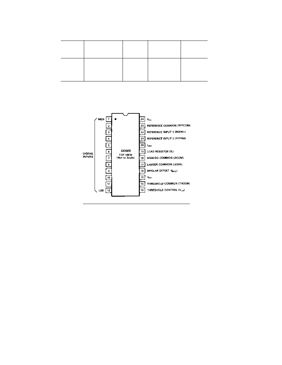
PIN CONFIGURATION

AD668
REV. A
≠5≠
ANALOG OFFSET ERROR: The analog offset is defined as
the offset of the analog amplifier channel, referred to the analog
input. Ideally, this would be measured with the analog input at
0 V and the digital input at full scale. Since a 0 V analog input
voltage constitutes an undervoltage condition, this specification
is determined through linear extrapolation, as indicated in
Figure 1.
Figure 1. Derivation of Analog Offset Voltage
GLITCH IMPULSE: Asymmetrical switching times in a DAC
may give rise to undesired output transients which are quanti-
fied by their glitch impulse. It is specified as the net area of the
glitch in pV-sec.
Figure 2. AD668 Major Carry Glitch
FUNCTIONAL DESCRIPTION
The AD668 is designed to combine excellent performance with
maximum flexibility. The functional block diagram and the
simple transfer functions provided below will provide the user
with a basic grasp of the AD668's operation. Examples of typi-
cal circuit configurations are provided in the section APPLY-
ING THE AD668. Subsequent sections contain more detailed
information useful in optimizing DAC performance in high
speed, high resolution applications.
DAC Transfer Function
The AD668 may be used either in a current output mode (DAC
output connected to a virtual ground) or a voltage output mode
(DAC output connected to a resistive load).
In current output mode:
Unipolar Mode
I
OUT
=
V
IN
V
NOM
◊
DAC code
4096
◊
10.24 mA
Bipolar Mode
I
OUT
=
V
IN
V
NOM
◊
DAC code
4096
◊
10.24 mA ≠
V
IN
V
NOM
◊
5.12 mA
In voltage output mode:
V
OUT
=
I
OUT
◊
R
LOAD
(for both unipolar and bipolar modes)
where:
V
IN
≠ the analog input voltage.
V
NOM
≠ the nominal full scale of the reference voltage: 1 V,
1.25 V, or 5 V, determined by the wiring configuration of Pins
21 and 22. (See APPLYING THE AD668.)
DAC code ≠ the numerical representation of the DAC's digital
inputs; a number between 0 and 4095.
R
LOAD
≠ the resistance of the DAC output node; the maximum
this can be is 200
(the internal DAC ladder resistance). The
on-board load resistor (Pin 19) has been trimmed so that its
parallel combination with the DAC ladder resistance is 100
(
±
1%)
Bipolar mode ≠ produces a bipolar analog output from the digital
input by offsetting the normal output current with a precision
current source. This offset is achieved by connecting Pin 16 to
the DAC output. In the unipolar mode, Pin 16 should be
grounded.
If the dc errors are included, the transfer function becomes
somewhat more complex:
I
OUT
=
V
IN
V
NOM
+
OFFSET
ANALOG
◊
DAC code
4096
◊
(1
+
E )
◊
10.24 mA
+
OFFSET
DIGITAL
◊
V
IN
V
NOM
◊
10.24 mA
≠
V
IN
V
NOM
+
OFFSET
ANALOG
◊
(5.12 mA
+
[OFFSET
BIPOLAR
◊
10.24 mA])
(Last term is for use in bipolar mode; V
OUT
is still just I
OUT
◊
R
LOAD
)
where:
OFFSET
ANALOG
= the analog offset error.
OFFSET
DIGITAL
= is the unipolar digital offset error.
OFFSET
BIPOLAR
= is the bipolar offset error.
E = the gain error, expressed fractionally.
Operating Limits:

AD668
REV. A
≠6≠
0.1
<
V
IN
V
NOM
<
1.2
0 < V
IN
/V
NOM
< 0.1 constitutes an undervoltage condition and
is subject to the specified recovery time.
1.2 < V
IN
/V
NOM
constitutes an overvoltage condition. This can
saturate the DAC transistors, resulting in decreased response
time and can, over extended time, damage the part through ex-
cessive power dissipation. Figure 3 indicates the specified re-
gions of operation in both the unipolar and bipolar cases.
The small signal 3 dB bandwidth of the V
IN
channel is 15 MHz.
The large signal 3 dB bandwidth is approximately 10 MHz.
V
OUT
is limited by the specified output compliance: ≠2 V to
+1.2 V.
Figure 3. Quadrant Plots of the AD668
CIRCUIT DESCRIPTION OF THE AD668
Successful design of high speed, high resolution systems de-
mands a designer's solid working knowledge of the components
being used. The AD668 has been carefully configured to pro-
vide maximum functionality in a variety of applications. While it
is beyond the scope of this data sheet to exhaustively cover each
potential application topology, the detailed information that
follows is intended to provide the designer with a sufficiently
thorough understanding of the part's inner workings to allow
selection of the circuit topology to best suit the application.
CURRENT OUTPUT VS. VOLTAGE-OUTPUT
As indicated in the FUNCTIONAL DESCRIPTION, the
AD668 output may be taken as either a voltage or a current,
depending on external circuit connections. In the current output
mode, the DAC output (Pin 20) is tied to a summing junction,
and the current flowing from the DAC into this summing junc-
tion is sensed. In this mode, the DAC output scale is insensitive
to whether the load resistor, R
LOAD
, is shorted (Pin 19 con-
nected to Pin 20), or grounded (Pin 19 connected to Pin 18).
However, the connection of this resistor does affect the output
impedance of the DAC and may have a significant impact on
the noise gain and stability of the external circuitry. Grounding
R
LOAD
will reduce the output impedance, thereby increasing the
noise gain and also enhancing the stability of a circuit using a
non-unity-gain-stable op amp (see Figure 10).
In the voltage output mode, the DAC's output current flows
through its own internal impedance (perhaps in parallel with an
external impedance) to generate a voltage. In this case, the DAC
output scale is directly dependent on the load impedance. The
temperature coefficient of the AD668's transfer function will be
lowest when used in the voltage output mode.
OUTPUT VOLTAGE COMPLIANCE
The AD668 has an output compliance range of ≠2.0 V to
+1.2 V (with respect to the LCOM pin). The current steering
output stages will be unaffected by changes in the output termi-
nal voltage over this range. However, as shown in Figure 4,
there is an equivalent output impedance of 200
in parallel
with 15 pF at the output terminal, producing an equivalent er-
ror current if the voltage deviates from the ladder common.
This is a linear effect which does not change with input code.
Operation beyond the maximum compliance limits may cause
either output stage saturation or breakdown, resulting in non-
linear performance. The positive compliance limit is not af-
fected by the positive power supply, but is a function of the
output current and the logic threshold voltage at V
TH
, Pin 13.
Figure 4. Equivalent Output Circuit
ANALOG INPUT CONSIDERATIONS
The reference input buffer can be viewed as a resistive divider
connected to one terminal of an op amp, as shown in Figure 5.
A unit DAC current source drives a resistor to produce a voltage
that is fed back to the opposite terminal of the op amp. Resistor
R
FEEDBACK
is laser-trimmed to ensure that a 1 V input to node A of
the op amp will produce a 10.24 mA DAC output. REFIN1 and
REFIN2 may be configured in any way the user chooses to pro-
vide a nominal input full scale of 1 V at node A. R1 and R2 are
sized and trimmed to provide both a 5:1 voltage divider and a
parallel impedance that matches the impedance at node B,
thereby reducing the amplifier offset voltage due to bias current.
The resistive divider is trimmed with an external 50
resistor in
series with the 4k leg (R2). This provides a gain trim range of
±
1%
using a 100
trim potentiometer (Figure 7). If trimming is not
desired, a 50
resistor may be used in place of the potentiom-
eter to produce the specified gain accuracy, or the resistor may
be omitted altogether to produce a nominal gain error of +1%.
Figure 5. Equivalent Analog Input Circuitry

AD668
REV. A
≠7≠
The variations in DAC settling and rise times can be attributed
to differences in rise time and current driving capabilities of the
various families. Differences in the glitch impulse are predomi-
nantly dependent upon the variation in data skew. Variations in
these specs occur not only between logic families, but also be-
tween different gates and latches within the same family. When
selecting a gate to drive the AD668 logic input, pay particular
attention to the propagation delay time specs: t
PLH
and t
PHL
.
Selecting the smallest delays possible will help to minimize the
settling time, while selection of gates where t
PLH
and t
PHL
are
closely matched to one another will minimize the glitch impulse
resulting from data skew. Of the common latches, the 74374
octal flip-flop provides the best performance in this area for
many of the logic families mentioned above.
PIN BY PIN CURRENT ACCOUNTING
The internal wiring and pinout of the AD668 are dictated in
large part by current management constraints. When using low
impedance, high current, high accuracy parts such as the
AD668, great care must be taken in the routing of not only sig-
nal lines, but ground and supply lines as well. The following ac-
counting provides a detailed description of the magnitudes and
signal dependencies of the currents associated with each of the
part's pins. These descriptions are consistent with the functional
block diagram as well as the equivalent circuits provided in Fig-
ures 4, 5, and 6.
V
CC
≠ the current into this pin is drawn predominantly through
the DAC current sources and generally runs about 2.2 times the
DAC's nominal full scale. By design, this current is independent
of the digital input code but is linearly dependent on analog in-
put variations.
REFCOM
≠ this node provides the reference ground for the
reference amplifier's current feedback loop (as illustrated in Fig-
ure 5) as well as providing the negative supply voltage for most
of the reference amplifier. The current consists of 1.2 mA of
analog input dependent current and another 3 mA of input in-
dependent current. Analog input voltages should always be pro-
duced with respect to this voltage.
REFIN1
≠ has a 1k series resistance to the reference amplifier
input and a 5k series resistance to REFIN2. REFIN1 may be
used in conjunction with REFIN2 to provide a 5:1 voltage di-
vider, or the two may be driven in parallel to provide a high
impedance input node (see Figure 5).
REFIN2
≠ the 4k side of the input resistive divider. Note also
that the combined impedance of these two resistors matches the
effective impedance at the other input of the reference amplifier,
thereby minimizing the offset due to bias currents. Circuits
which alter this effective impedance may suffer increased analog
offset and drift performance degradation as a result of the mis-
match in these impedances.
I
OUT
≠ the output current. In the current output mode with this
node tied to a virtual ground, a 10.24 mA nominal full scale
output current will flow from this pin. In the voltage output
mode, with R
L
grounded, half of the output current will flow
out of R
L
and the other half will flow out of LCOM. External
resistive loading will cause current to be divided between
LCOM, R
L
, and I
OUT
as Figure 4 suggests.
DIGITAL INPUT CONSIDERATIONS
The AD668 uses a standard positive true straight binary code
for unipolar outputs (all 1s full-scale output), and an offset bi-
nary code for bipolar output ranges. In the bipolar mode, with
all 0s on the inputs, the output will go to negative full scale;
with 111 . . . 11, the output will go to positive full scale less
1 LSB; and with 100 . . . 00 (only the MSB on), the output will
go to zero.
The threshold of the digital inputs is set at 1.4 V and does not
vary with supply voltage. This reference is provided by a band-
gap generator, which requires approximately 3 mA of bias
current achieved by tying R
TH
to any +V
LOGIC
supply where:
R
TH
=
+
V
LOGIC
≠ 1.4 V
3 mA
(see Figure 6). The digital bit inputs operate with small input
currents to easily interface to unbuffered CMOS logic. The digi-
tal input signals to the DAC should be isolated from the analog
input and output as much as possible. To minimize undershoot,
ringing, and digital feedthrough noise, the interconnect distance
to the DAC inputs should be kept as short as possible. Termina-
tion resistors may improve performance if the digital lines be-
come too long. The digital inputs should be free from large
glitches and ringing and have 10% to 90% rise and fall times on
the order of 5 ns.
Figure 6. Equivalent Digital Input
To realize the AD668's specified ac performance, it is recom-
mended that high speed logic families such as Schottky TTL,
high speed CMOS, or the new lines of high speed TTL be used
exclusively. Table I shows how DAC performance, particularly
glitch, can vary depending on the driving logic used. As this
table indicates, STTL, HCMOS, and FAST* represent the
most viable families for driving the AD668.
Table I. DAC Performance vs. Drive Logic
10%-90%
2
Settling Time
2, 3
Maximum
Logic
DAC Rise
1 LSB
Glitch
4
Glitch
Family
1
Time
1%
0.1% (0.025%)
Impulse Excursion
TTL
10.5 ns
47 ns 77 ns 100 ns
2.5 nV-s
280 mV
LSTTL
11.25 ns
35 ns 60 ns 120 ns
1.2 nV-s
270 mV
STTL
11 ns
50 ns 75 ns 110 ns
500 pV-s 200 mV
HCMOS 12 ns
53 ns 78 ns 100 ns
350 pV-s 200 mV
FAST*
11.5 ns
49 ns 73 ns 100 ns
2 nV-s
250 mV
NOTES
1
All values typical, taken in test fixture diagrammed in Figure 23.
2
Measurements are made for a 1 V full-scale step into 100
DAC load resistance.
3
Settling time is measured from the time the digital input crosses the threshold
voltage (1.4 V) to when the output is within the specified range of its final value.
4
The worst case glitch impulse, measured on the major carry. DAC full scale is1 V.
*FAST is a registered trademark of National Semiconductor Corporation.
AD668
REV. A
≠8≠
R
L
≠ a 200
resistor with one end internally wired to the out-
put pin. If a 200
±
20% DAC output impedance is desired, R
L
should be shorted to I
OUT
. Grounding R
L
will provide a DAC
output impedance of 100
±
1%. As noted above, in voltage
output configurations, a large portion of the DAC output cur-
rent will flow through this pin.
ACOM
- as indicated in Figure 4, the current flowing out of
this pin is effectively the complement of I
OUT
, varying with both
analog and digital inputs. Using this current as a signal output is
not generally advised, since it is untrimmed and its positive out-
put compliance is limited to the logic low voltage.
LCOM
- the current in this node has been carefully configured
to be independent of digital code when the output is into a vir-
tual ground, thereby minimizing any detrimental effects of lad-
der ground resistance on linearity. However, the current in this
node is proportional to the analog input voltage and the ground
drop here is responsible for the dc analog feedthrough. The
nominal value of this current is approximately equal to the DAC
full scale.
IBPO
- the bipolar offset current flows into this node, with volt-
age compliance to V
EE
+ 3V. This is a high impedance current
source, and should be grounded if the offset current is not used.
V
EE
- this voltage may be set anywhere from ≠10.8 V to
≠16.5 V. The current in this node consists of 1.2 times the bipo-
lar offset current plus 500
µ
A of bias current for the reference
amplifier's front end. The negative supply current is indepen-
dent of digital input but is linearly dependent on analog input.
THCOM
- is the ground point for the bandgap diode that gen-
erates the threshold voltage. The current coming out of this
node is the same as that flowing into V
TH
plus a code dependent
number of base currents (see Figure 6). It is possible to intro-
duce an offset between THCOM and the system common,
thereby offsetting the effective logic threshold and positive out-
put compliance voltage.
V
TH
- as indicated earlier, if given sufficient positive bias cur-
rent, this voltage will be 1.4 V above THCOM. The necessary
bias current can readily be provided by a suitable resistor to any
positive supply. As Figure 6 suggests, this node is directly
coupled to the DAC output through several base to collector
capacitances and hence, should be carefully decoupled to the
analog ground.
DIGITAL INPUTS
- when a bit is in the high state, the input
current is the leakage current of a reverse biased diode. When
the bit is driven low, it must sink a base current to ground, and
this base current will be proportional to the analog input. Note
that the input current for Bit 2 will be twice that for Bits 3-12,
and Bit 1's current will be 4 times Bit 3's, but all the currents
will be below the value specified.
APPLYING THE AD668
The following are some typical circuit configurations for the
AD668. As Table II indicates, these represent only a sample of
the possible implementations.
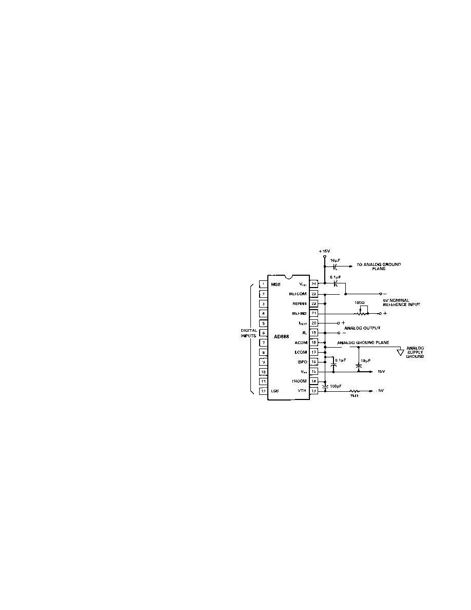
5 V REFIN, 1 V UNIPOLAR, UNBUFFERED VOLTAGE
OUTPUT
Figure 7 shows a typical topology for generating an unbuffered
voltage output. R
L
(Pin 19) is grounded, producing a 100
DAC output resistance that generates a 1.024 V output when
the DAC current is at its full scale of 10.24 mA. The presence
of low impedance loads will effect the output voltage swing di-
rectly: an external load of 300
will yield a total output resis-
tance of 75
, and a full scale output of 0.768 V. An external
100
will reduce the total output resistance to 50
and the
full-scale voltage swing will drop to 0.512 V. Since the bipolar
offset current is not used in this configuration, Pin 16 is con-
nected to the analog ground plane.
The input divider has been connected to produce a 5 V full
scale reference input by shorting REFIN1 to the analog ground
plane and using REFIN2 as the reference input. With a 5 V
nominal full scale, the 10% to 120% reference input range falls
between 0.5 V and 6 V. The effective input resistance in this
mode is 5 k
(
±
20%). The ratio of the input divider has been
intentionally skewed by 50
to provide an optional external
fine trim for gain adjust. A trim range of
±
1% is provided by the
100
trimming potentiometer shown in Figure 7. If trimming
is not desired, a 50
resistor may be used in place of the poten-
tiometer to produce the specified gain accuracy, or, if a +1%
nominal gain error is tolerable, the resistor may be omitted
altogether.
Figure 7. 5 V REFIN/1 V Unbuffered Unipolar Output
1.25 V REFIN, 1 V BIPOLAR, UNBUFFERED VOLTAGE
OUTPUT
Figure 8 demonstrates another unbuffered voltage output topol-
ogy, this time implementing a bipolar output and a 1.25 V refer-
ence input. The bipolar output is accomplished simply by tying
Pin 16 to the output (Pin 20). Note that in this mode, when the
digital inputs are all zeros and the analog input is at 1.25 V,
≠512 mV will be produced at the DAC output. Bipolar zero
(0 V
OUT
) will be produced when the MSB is ON with all other
bits OFF (100 . . . 00), and the full-scale voltage minus 1 LSB
(511.75 mV) will be generated when all bits are ON.
The input range of 1.25 V is generated by grounding REFIN2
(through an optional gain trim potentiometer or gain adjust
50
resistor) and using REFIN1 as the reference input. The
input resistance in this mode is also 5k.

AD668
REV. A
≠9≠
Figure 8. 1.25 V REFIN/
±
500 mV Unbuffered Bipolar
Output
5 V REFIN, 2 V BIPOLAR, UNBUFFERED VOLTAGE
OUTPUT
Figure 9 demonstrates how a larger unbuffered voltage output
swing can be realized. R
LOAD
(Pin 19) is tied to the DAC output
(Pin 20) to produce an output resistance of roughly 200
.
Figure 9. 5 V REFIN/
±
1 V Unbuffered Bipolar Output
It should be noted that this impedance is not trimmed, and may
vary by as much as 20%, but this can be compensated by adjust-
ing the reference voltage. It is also important to note that limita-
tions in the DAC output compliance would prohibit use of a 2 V
unipolar output voltage swing.
1 V REFIN, ≠10 V UNIPOLAR, BUFFERED VOLTAGE
OUTPUT
Figure 10 shows the implementation of the 1 V full scale for the
reference input by tying REFIN1 and REFIN2 together and
driving them both with the input voltage. This generates a high
input impedance, and some care should be taken to insure that
the driving impedance at this node is finite at all times to avoid
saturating the reference amplifier. This is typically accomplished
by a using a low impedance voltage source to drive the refer-
ence, but if the topology calls for this source to be switched out,
a high impedance (10 k
) termination resistor should be used
on the REFIN node.
Figure 10. 1 V REFIN/≠10 V Unipolar Buffered Output
For full-scale output ranges greater than 2 V, some type of ex-
ternal buffer amplifier is needed. The AD840 fills this require-
ment perfectly, settling to within 0.025% from a 10 V full-scale
step in less than 100 ns. As shown in Figure 10, the amplifier
establishes a summing node at ground for the DAC output. The
output voltage is determined by the amplifier's feedback resistor
(10.24 V for a 1k resistor). Note that since the DAC generates a
positive current to ground, the voltage at the amplifier output
will be negative. A series resistor between the noninverting am-
plifier input and ground minimizes the offset effects of op amp
input bias currents.
The optimal DAC output impedance in buffered output appli-
cations depends on the buffer amplifier being used. The AD840
is stable at a gain of 10, so a lower DAC output impedance
(higher noise gain) is desired for stability reasons, and R
LOAD
should be grounded. The 100
DAC output impedance pro-
duces a noise gain of 11 with the 1k feedback resistor. If the
gain-of-two stable AD842 is used as a buffer, a 200
DAC out-
put impedance will produce a stable configuration with lower
noise gain to the output; hence, R
LOAD
should be connected to
the DAC output.
As noted earlier, these four examples are part of an array of
possible configurations available. Table II provides a quick
reference chart for the more straightforward applications, but
many other input and output signals are possible with some
modifications.
The next three circuits provide examples of different analog in-
put drives, including a fixed dc reference, a capacitively coupled
ac reference, and a DAC driving the reference channel. Note
that the entire spectrum of input and output range configura-
tions are available regardless of the type of reference drive being
used.
DC REFERENCE: THE AD586 DRIVING THE AD668
Figure 11 illustrates one of the more obvious analog input
sources: a fixed reference. The AD586 produces a temperature
stable 5 V analog output to drive the AD668 in the 5 V input

AD668
REV. A
≠10≠
Figure 11. AD586 Driving the AD668
mode (Pin 22 grounded, input into Pin 21). Fine adjustment of
the gain is provided by both the AD586 external trim resistor
and the 100
potentiometer in series with the reference input.
The resistive divider at the reference input will draw approxi-
mately 1 mA from the AD586, leaving plenty of driving current
for other loads in the system.
AC HOOKUP: 1.25 V AC FULL SCALE, 2.5 V DC FULL
SCALE
The circuit shown in Figure 12 allows separate setting of dc ref-
erence bias point on a 2.5 V scale and capacitively coupled ac
signal on a 1.25 V scale. The basic reference input is configured
in the 1.25 V mode (Pin 21 grounded, Pin 22 used as the refer-
ence input.) The 2.5 V dc range is achieved by using an external
Table II. AD668 Topology Variations
OUTPUT LEVELS
Nominal
Analog
Input
0 V to 1 V
≠500 mV to +500 mV
0 V to ≠10 V
+5 V to ≠5 V
≠1 V to +1 V
Unipolar
Bipolar
Unipolar
Bipolar
Bipolar
1 V
Unbuffered V
OUT
Unbuffered V
OUT
Buffered V
OUT
Buffered V
OUT
Unbuffered V
OUT
A
IN
= Pins 21 + 22
A
IN
= Pins 21 + 22
A
IN
= Pins 21 + 22
A
IN
= Pins 21 + 22
A
IN
= Pins 21 + 22
External Amplifier
External Amplifier
R
L
(Pin 19) Tied
(See Figure 10)
To I
OUT
(Pin 20)
Unipolar
Bipolar
Unipolar
Bipolar
Bipolar
Unbuffered V
OUT
Unbuffered V
OUT
Buffered V
OUT
Buffered V
OUT
Unbuffered V
OUT
1.25 V
A
IN
= Pin 22
A
IN
= Pin 22
A
IN
= Pin 22
A
IN
= Pin 22
A
IN
= Pin 22
Pin 21 Grounded
Pin 21 Grounded
Pin 21 Grounded
Pin 21 Grounded
Pin 21 Grounded
(See Figure 8)
External Amplifier
External Amplifier
R
L
(Pin 19) Tied
To I
OUT
(Pin 20)
Unipolar
Bipolar
Unipolar
Bipolar
Bipolar
Unbuffered V
OUT
Unbuffered V
OUT
Buffered V
OUT
Buffered V
OUT
Unbuffered V
OUT
5 V
A
IN
= Pin 21
A
IN
= Pin 21
A
IN
= Pin 21
A
IN
= Pin 21
A
IN
= Pin 21
Pin 22 Grounded
Pin 22 Grounded
Pin 22 Grounded
Pin 22 Grounded
Pin 22 Grounded
(See Figure 7)
External Amplifier
External Amplifier
R
L
(Pin 19) Tied
To I
OUT
(Pin 20)
(See Figure 9)
5k series resistor in the dc path. Note that because of the rela-
tively wide tolerance (
±
20%) in the absolute value of the
AD668's internal input divider resistors, substantial gain range
adjustment should be provided in the external series resistance.
Figure 12. AC Hookup
DAC DRIVE: THE AD568 DRIVING THE AD668
The circuit shown in Figure 13 produces an analog output pro-
portional to the product of two digital inputs. The AD568 has
an on-board fixed reference and generates a full-scale output
voltage of 1.024 V (just as the AD668 does in its unbuffered
voltage output mode). This output voltage can be used to di-
rectly drive the AD668 in the 1 V reference input mode. Note
that in this case, the lower 410 codes of the AD568 are out-of-
bounds; they produce an undervoltage condition at the AD668

AD668
REV. A
≠11≠
reference input. While the two DACs are similar in many ways,
the optimal decoupling schemes differ between the two parts
and care should be used to insure that each is implemented
appropriately.
Figure 13. AD568 Driving the AD668
CONSTRUCTION GUIDELINES
HIGH FREQUENCY PRINTED CIRCUIT BOARD
SUGGESTIONS
In systems seeking to simultaneously achieve high speed and
high accuracy, the implementation and construction of the cir-
cuit is often as important as the circuit's design. Proper RF
techniques must be used in device selection, placement and
routing, and supply bypassing and grounding. In many areas,
the performance of the AD668 may exceed the measurement ca-
pabilities of common lab instruments, making performance
evaluation particularly difficult. The AD668 has been config-
ured to be relatively easy to use in spite of these problems, and
realization of the performance indicated in this datasheet should
not be difficult if proper care is taken. Figure 14 provides an il-
lustration of the printed circuit board layout used for much of
the AD668's characterization. The board represents an imple-
mentation of the circuit shown in Figure 23, with the AD586
used to drive the reference channel (as in Figure 11).
Component Side
Foil Side
Figure 14. PC Board Layout
THE USE OF GROUND AND POWER PLANES
If properly implemented, ground planes can perform a myriad
of functions on high speed circuit boards: bypassing, shielding,
current transport, etc. In mixed signal design, the analog and
digital portions of the board should be distinct from one an-
other, with the analog ground plane confined to areas covering
analog signal traces and the digital ground plane confined to
areas covering digital interconnect. The two ground planes
should be connected by paths 1/4 inch to 1/2 inch wide on both
sides of the DAC, as shown in Figure 14. Care should be taken
to insure that the ground plane is uninterrupted over crucial sig-
nal paths. On the digital side, this includes the digital input lines
running to the DAC, as well as any clock signals. On the analog
side, this includes the analog input signal, the DAC output sig-
nal, and the supply feeders. The use of wide runs or planes in
the routing of the power supplies is also recommended. This
serves the dual function of providing a low series impedance
power supply to the part as well as providing some "free" ca-
pacitive decoupling to the appropriate ground plane.
USING THE RIGHT BYPASS CAPACITORS
The capacitors used to bypass the power supplies are probably
the most important external components in any high speed de-
sign. Both selection and placement of these capacitors can be
critical and, to a large extent, dependent upon the specifics of
the system configuration. The dominant consideration in the
selection of bypass capacitors for the AD668 is minimization of
series resistance and inductance. Many capacitors will begin to
look inductive at 20 MHz and above. Ceramic and film type
capacitors generally feature lower series inductance than tanta-
lum or electrolytic types. A few general rules are of universal use
when approaching the problem of bypassing.
Bypass capacitors should be installed on the printed circuit
board with the shortest possible leads consistent with reliable
construction. This helps to minimize series inductance in the
leads. Chip capacitors are optimal in this respect.
Some series inductance between the DAC supply pins and the
power supply plane may help to filter-out high frequency power
supply noise. This inductance can be generated using a small
ferrite bead.

AD668
REV. A
≠12≠
HIGH SPEED INTERCONNECT AND ROUTING
It is essential that care be taken in the signal and power ground
circuits to avoid inducing extraneous voltage drops in the signal
ground paths. It is suggested that all connections be short, di-
rect, and as physically close to the package as possible, thereby
minimizing the sharing of conduction paths between different
currents. When runs exceed an inch or so in length, some type
of termination resistor may be required. The necessity and value
of this resistor will be dependent upon the logic family used.
For maximum ac performance, the DAC should be mounted di-
rectly to the circuit board; sockets should be avoided as they in-
troduce unwanted capacitive coupling between adjacent pins of
the device. For purposes of testing and characterization, low
profile sockets are preferable to zero insertion force types.
TYPICAL PERFORMANCE CHARACTERISTICS
The following plots indicate the typical performance of the
AD668 in properly configured circuits. Wherever possible, sug-
gestions are provided to assist the user in achieving the indicated
performance levels.
DC PERFORMANCE
Power Consumption vs. V
REF
/V
NOM
As suggested in previous sections, most portions of AD668's
current budget are proportional to the analog input signal. As a
result, operating the part at a reduced reference voltage offers
substantial power savings. This may be particularly attractive in
applications featuring a buffered output voltage, since the size of
the feedback resistor may be increased to compensate for the re-
duced DAC current. For example, the DAC could be config-
ured in the 5 V input mode, but driven with a 2.5 V reference,
producing a 5.12 mA full scale output. Reducing the output
level has performance ramifications in several areas, as demon-
strated later in this section, but the circuit designer is free to
trade power dissipation against performance to optimize the
AD668 for his application.
Figure 15. Power Consumption vs. Reference Level
Linearity vs. V
REF
/V
NOM
At reduced current levels, the linearity of the PNP DAC used in
the AD668 becomes more sensitive to the mismatch in transis-
tor V
BE
's. As Figure 16 indicates, this effect starts to increase
fairly dramatically for reference levels less than 25% of nominal.
Increasing the current level above 100% does not appreciably
improve the linearity performance since the DAC has been
trimmed to perform optimally at the 100% reference level.
Figure 16. Linearity vs. Reference Level
AC PERFORMANCE
For the purposes of characterizing the frequency domain perfor-
mance of the AD668, all bits are turned on and the DAC is es-
sentially treated as a voltage amplifier/attenuator. The tests used
to generate these performance curves were done using the cir-
cuit shown in Figure 12.
AC characterization in the megahertz region is not trivial, and
special consideration is required to produce meaningful results.
Probe ground straps are inappropriate at these frequencies;
some type of probe socket is required. Signals should be routed
either on a PC board over a ground plane or through a coaxial
cable. Proper termination impedances should be used through-
out the fixturing.
Large Signal Frequency Response
Figure 17 represents the gain and phase response of a signal
swinging from 10% to 120% (peak to peak) of the nominal ref-
erence input. The DAC reference amplifier has an effective slew
rate or 30 V/
µ
s at the DAC output, so there will be slew-induced
distortion for full scale swings at greater than 10 MHz.
Figure 17. Large Signal Gain and Phase Response
Small Signal 3 dB Bandwidth vs. V
REF
/V
NOM
Figure 18 demonstrates the small signal (20% of nominal refer-
ence) bandwidth sensitivity to the analog input's dc bias. The
small signal 3 dB bandwidth at 100% reference levels is greater
than 15 MHz, but the bandwidth remains greater than 10 MHz
over the entire nominal reference range. The differential gain
and phase for a 200 mV, 3 MHz signal are 0.5% and 2
∞
,
respectively.

AD668
REV. A
≠13≠
Figure 18. Small Signal Bandwidth vs. DC Reference Level
Noise Spectrum
Figure 19 shows the noise spectrum of the DAC with all bits on.
The noise floor of ≠78 dB is just above the noise floor of the in-
strument being used, in part due to the relatively small (1 V)
output signal of the DAC in voltage output mode.
Figure 19. Noise Spectrum
Analog Feedthrough vs. Frequency
Analog feedthrough is a measure of the effective signal at the
DAC output when all bits are off and a full-scale signal is placed
at the analog input. At dc, the feedthrough is a result of analog
input dependent ground drops, predominantly through the lad-
der ground. Good grounding practices will minimize this effect.
At high frequencies, the signal may propagate to the output
through a variety of capacitive paths. Proper shielding and rout-
ing should be implemented to eliminate external coupling be-
tween the analog input and the DAC output node.
Figure 20. Analog Feedthrough vs. Frequency
Reference Channel THD
THD, or total harmonic distortion, is the ratio of the
rootmean-square (rms) sum of the harmonics to the fundamen-
tal and is expressed in dBs. Figure 21 shows the typical THD of
the AD668 reference channel for both large and small signals.
Figure 21. Reference Channel THD vs. Frequency
TRANSIENT PERFORMANCE
High accuracy settling time measurements of less than one hun-
dred nanoseconds are extremely diliicult to make. The conven-
tional analog amplifiers used in oscilloscope front ends,
typically, cannot recover from the overdrive resulting from a
full-scale step in sufficient time. Sampling scopes can track
much quicker rise times but often provide insufficient accuracy
for 12-bit characterization. Data Precision's new 640 sampling
scope provides a good combination of speed and resolution that
provides just enough performance to measure the AD668's
performance.
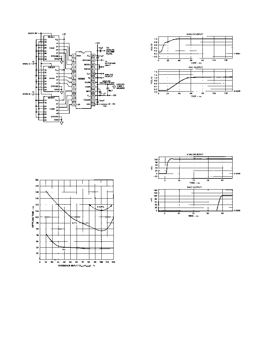
Digital Settling Time
Figure 22 illustrates the typical settling characteristic of the
AD668 to a full-scale change in digital inputs with the analog
input fixed at 100%. The digital driving circuity is shown in
Figure 23. This circuit allows the DAC to be toggled between
any two codes, and so provides an excellent means of character-
izing both settling and glitch performance.
Figure 22. Typical Digital Settling Characteristics
AD668
REV. A
≠14≠
Figure 23. Settling Time Circuit
Digital Settling Time vs. V
REF
The reference amplifier loop has been compensated for optimal
settling performance at V
REF
/V
NOM
= 100%, but as Figure 24
indicates, there is relatively little degradation in settling perfor-
mance for a wide range of reference levels. Consideration of
Figures 15, 16, and 24 support that a 1/2 power solution would
see very little degradation in speed or accuracy performance.
Figure 24. Digital Settling Time vs. Reference Level
Analog Settling Time
One of the biggest challenges in measuring the settling time of a
high accuracy amplifier is producing a clean waveform with
which to drive the input. In this case, an AD568 was used to
drive the analog channel in the 1 V input mode (see Figure 13).
As indicated by Figure 25, the referred-to-output slew rate is
30 V/
µ
s for a 1 V output. This implies that a full-scale analog
input sine waves of greater than 10 MHz frequency will suffer
some slew-induced distortion. It should be noted that the
slewing limitation is in the reference amplifier, not in the DAC
output, so a 10 V buffered output voltage would slew at
300 V/
µ
s, provided the output buffer is sufficiently fast.
Figure 25. Typical Analog Settling Characteristic
Undervoltage Recovery Time
The ramifications of exceeding the specified lower limit of 10%
on the reference channel depend on the extent and duration of
the undervoltage condition. Figure 26 illustrates that, after hold-
ing the reference at 0% (REFIN = REFCOM) for 1
µ
s, the
AD668 takes 35 ns to return to 10% of full scale once the refer-
ence is returned to 100%. This is the worst case: recovery from
a completely "off" condition.
Figure 26. Undervoltage Recovery
Glitch Impulse
The AD668's glitch at the major carry is illustrated in Figure 2.
The AD668 features a conventional DAC architecture that has
two basic glitch mechanisms: digital feedthrough and data skew.
Careful consideration of these mechanisms will help the glitch-
conscious user minimize glitch in his application.
Digital Feedthrough
As with any converter product, a high speed digital-to-analog
converter is forced to exist on the frontier between the noisy
environment of high speed digital logic and the sensitive analog
domain. The problems of this interfacing are particularly acute
when demands of high speed (greater than 10 MHz switching
times) and high precision (12 bits or more) are combined. No
amount of design effort can perfectly isolate the analog portions
of a DAC from the spectral components of a digital input signal
with a 2 ns rise time. Inevitably, once this digital signal is
brought onto the chip, some of its higher frequency components
will find their way to the sensitive analog nodes, producing a
digital feedthrough glitch. To minimize the exposure to this ef-
fect, the AD668 has intentionally omitted the on-board latches
that have been included in many slower DACs. This not only
reduces the overall level of digital activity on chip, it also avoids

AD668
REV. A
≠15≠
bringing a latch clock pulse on board, whose opposite edge in-
evitably produces a substantial glitch, even when the DAC is not
supposed to be changing codes.
Data Skew
The AD668, like many of its slower predecessors, essentially
uses each digital input line to switch a separate, weighted cur-
rent to either the output (I
OUT
) or some other node (ANALOG
COM). If the input bits are not changed simultaneously, or if
the different DAC bits switch at different speeds, then the DAC
output current will momentarily take on some incorrect value.
This effect is particularly troublesome at the "carry points,"
where the DAC output is to change by only one LSB, but sev-
eral of the larger current sources must be switched to realize this
change. Data skew can allow the DAC output to move a sub-
stantial amount towards full scale or zero (depending upon the
direction of the skew) when only a small transition is desired.
Great care was taken in the design and layout of the AD668 to
ensure that switching times of the DAC switches are symmetri-
cal and that the length of the input data lines are short and well
matched. The glitch-sensitive user should be equally diligent
about minimizing the data skew at the AD668's inputs, particu-
larly for the 4 or 5 most significant bits. This can be achieved by
using the proper logic family and gate to drive the DAC, and
keeping the interconnect lines between the log outputs and the
DAC inputs as short and as well matched as possible, particu-
larly for the most significant bits. The top 6 bits should be
driven from the same latch chip if latches are used.
DEGLITCHING FOR PRECISION WAVEFORM
GENERATION
There are high speed SHAs available with specifications suffi-
cient to deglitch the AD668, however most are hybrid in design
at costs which can be prohibitive. A high performance, low cost
alternative shown in Figure 27 is a discrete SHA utilizing a high
speed monolithic op amp and high speed DMOS FET switches.
This SHA circuit uses the inverting integrator architecture. The
AD841 operational amplifier used (300 MHz gain bandwidth
product) is fabricated on the same high speed process as the
AD668. The time constant formed by the 100
resistor and the
100 pF capacitor determines the acquisition time and also band
limits the output signal to eliminate slew induced distortion.
A discrete drive circuit is used to achieve the best performance
from the SD5000 quad DMOS switch. This switch driving cell
is composed of MPS571 RF npn transistors and an MC10124
TTL to ECL translator. Using this technique provides both
high speed and highly symmetrical drive signals for the SD5000
switches. The switches are arranged in a single-throw double-
pole (SPDT) configuration. The 360 pF "flyback" capacitor is
switched to the op amp summing junction during the hold mode
to keep switching transients from feeding to the output. This
capacitor is grounded during sample mode to minimize its effect
on acquisition time.
Circuit layout for a high speed deglitcher is almost as critical as
the design itself. Figure 28 shows the recommended layout of
the deglitching cell for a double-sided printed circuit board. The
layout is very compact with care taken that all critical signal
paths are short.
Performance of the AD668 in waveform generation applications
is greatly improved with the use of this deglitching method. Peak
harmonics and spurious free dynamic range are typically main-
tained at -70 dB to -75 dB with update rates up to 10 MHz.
4
5
10
6
5
16
8
9
2
4
AD841
5V
≠
5V
+
MC
10124
15V
≠
R11
20k
TO PIN 2
SD5000
C1
0.039
µ
F
R12
1.6k
S/
H
5V
≠
5V
≠
15V
≠
R6
249
R7
169
R8
510
R10
249
R9
169
R5
360
R4
360
MPS 571
(2)
D1
IN4735
INPUT
R1
100
R2
100
13
12
14
16
11
9
100pF
C
FILT
6
3
8
5
4
1
360pF
C
HOLD
R3
100
OUTPUT
15V
+
Figure 27.
High Performance, Low Cost Deglitching Circuit

AD668
REV. A
≠16≠
C1451≠10≠9/90
PRINTED IN U.S.A.
OUTLINE DIMENSIONS
Dimensions shown in inches and (mm).
24-Pin Cerdip (Suffix Q)
Figure 28a. PCB Layout of Foil Side
Figure 28b. PCB Layout of Component Side