 | ÐлекÑÑоннÑй компоненÑ: AD6411 | СкаÑаÑÑ:  PDF PDF  ZIP ZIP |
Äîêóìåíòàöèÿ è îïèñàíèÿ www.docs.chipfind.ru
REV. 0
Information furnished by Analog Devices is believed to be accurate and
reliable. However, no responsibility is assumed by Analog Devices for its
use, nor for any infringements of patents or other rights of third parties
which may result from its use. No license is granted by implication or
otherwise under any patent or patent rights of Analog Devices.
a
AD6411
One Technology Way, P.O. Box 9106, Norwood, MA 02062-9106, U.S.A.
Tel: 781/329-4700
World Wide Web Site: http://www.analog.com
Fax: 781/326-8703
© Analog Devices, Inc., 1998
DECT RF Transceiver
FUNCTIONAL BLOCK DIAGRAM
LNA
PA
RSSI
RX
DATA
TX
DATA
AD6411
PLL
DEMODULATOR
PLL
VCO
CONTROL
INTERFACE
PFD
FEATURES
Fully Compliant with DECT Specifications
Single IC DECT Radio
Integrated UHF VCO (External Resonator)
Integrated Synthesizer Supporting Extended Frequency
Allocation
Built-In Supply Regulation
Direct VCO Modulation for DECT Transmit Path
PLL-Based Demodulator
Use with Low Cost Plastic Packaged SAW Filters
Ultralow Power Design
Operates from +3.0 V to +5.5 V Battery
User-Selectable Power-Down Modes
Small 48-Lead LQFP Package
APPLICATIONS
DECT Cordless Telephones
DECT-Based Wireless Local Loop Systems
DECT-Based Wireless Data Systems
DESCRIPTION
The AD6411 provides the complete transmit and receive RF
signal processing necessary to implement a digital wireless
transceiver based on the Digital Enhanced Cordless Telecom-
munications (DECT) standard.
The AD6411's receive signal path consists of a mixer, IF ampli-
fiers and PLL demodulator. The low noise, high intercept mixer
is a development of the doubly-balanced Gilbert-Cell type. It
has a nominal 16 dBm input-referred 1 dB compression point
and a 8 dBm input referred third-order intercept. The limiter
amplifier provides sufficient gain to drive the PLL demodulator,
which provides selectable analog or sliced outputs. The RSSI
output provides a voltage proportional to the receive signal
strength. It measures nearly 100 dB IF signal strength range
with 14 mV/dB gain scaling.
The transmit path accepts baseband data, which is filtered and
applied to the VCO directly. The VCO operates at half the RF
carrier frequency, and is doubled to avoid pulling due to leakage
from the output.
An on-chip PLL frequency synthesizer provides channel selec-
tion. Operating modes are selected either through a serial bus or
asynchronous control pins. This allows compatibility with most
of the available DECT baseband controller ASICs.
The AD6411 is packaged in a 48-lead LQFP.

2
REV. 0
AD6411SPECIFICATIONS
(T
A
= 25 C, 3.0 V < V
BAT
< 5.5 V unless otherwise noted)
Parameter
Conditions
Min
Typ
Max
Units
RECEIVE RF MIXER
RF Input Frequency
1880 to
1930
MHz
Power Gain
Z
SOURCE
= 50
, Z
LOAD
= 200
15
19
21
dB
Input 1 dB Compression Point
Z
SOURCE
= 50
, Z
LOAD
= 200
21
16
dBm
Input Third-Order Intercept
Z
SOURCE
= 50
, Z
LOAD
= 200
8
dBm
SSB Noise Figure
Z
SOURCE
= 50
, Z
LOAD
= 200
11
dB
Output VSWR
100 MHz120 MHz
1.5:1
Output Impedance
200
Input Impedance
50
RX IF AMPLIFIERS
Differential Input Impedance
200
Input VSWR
Input Power < 11 dBm
1.5:1
IF Noise Figure
Z
SOURCE
= 200
Differential
6
dB
RSSI
RSSI Upper Limit
Z
SOURCE
= 200
Differential
5
+3
dBm
RSSI Lower Limit
Z
SOURCE
= 200
Differential
95
dBm
RSSI High Level Voltage
Input Power = 0 dBm (at IF Input)
1.7
V
RSSI Low Level Voltage
Input Power = 90 dBm (at IF Input)
0.3
V
RSSI Slope
90 dBm < Input Power < 0 dBm (at IF Input)
14
mV/dB
RSSI Output Impedance
V
RSSI
= 0.3 V
700
RSSI Output Response Time
Settling to 95% Value for a 40 dB Input Step,
20 pF External Load
2
µ
s
PLL DEMODULATOR
PLL Demodulator Phase Detector Gain
@ 90 Degree Relative Phase
80
115
150
µ
A/rad
Leakage Current at COFF
Charge Pump Disabled
100
pA
Recommended External VCO Gain
1.152
MHz/V
Demodulator Gain
VCO Gain Set to 1.152 MHz/V
1.736
V/MHz
Demodulator Linearity
THD for FM Tone @ 576 kHz,
Peak Deviation 288 kHz
30
dBc
VOLTAGE REFERENCE
Output Voltage
1.3
1.37
1.44
V
Output Current
100
µ
A
TRANSMIT SECTION
Output Power
Z
L
= 50
3
+1
+4
dBm
Harmonically Related Spurii
At 0.5
×
DECT_Tx: (940 MHz950 MHz)
10
dBc
At 1.5
×
DECT_Tx: (2820 MHz2850 MHz)
20
dBc
Other Spurii
100 MHz3000 MHz, Outside DECT Band
1 MHz Measurement Bandwidth
73
dBc
Output Phase Noise
With UHF Resonator Qu > 30
1.2 MHz
120
dBc/Hz
3.0 MHz
130
dBc/Hz
>4.7 MHz
135
dBc/Hz
VCO Operating Frequency Range
With Suitable External Resonator
700
1200
MHz
Oscillator Push
Using On-Chip Regulator, 250 mV V
BAT
Step Change with 5
µ
s Rise/Fall Time
6
kHz
Oscillator Pull
VSWR = 2:1 Any Phase
55
kHz
SYNTHESIZER
Reference Input Impedance
>5
k
Reference Input Level
100
1000
mV p-p
Reference Input Frequency
10
20
MHz
VCO Signal Input Range
700
1200
MHz
Charge Pump Current "Up"
Voltage On Loop Filter (Pin 38) = 1.4 V
1.30
1.0
0.77
mA
Charge Pump Current "Down"
Voltage On Loop Filter (Pin 38) = 1.4 V
0.66
1.0
1.15
mA
Charge Pump Leakage
Output Disabled
<
±
1
nA
BSW Output "High" Voltage
at I
LOAD
< = 2 mA
2.5
V
3
REV. 0
AD6411
Parameter
Conditions
Min
Typ
Max
Units
VOLTAGE REGULATORS (VS1, VS2)
Regulated Voltage Output
I
LOAD
= 60 mA max
2.675
2.725
2.825
V
Dropout Voltage
I
LOAD
= 60 mA; BCW68F or
Equivalent Pass Transistor
150
mV
Load Regulation
VS1: 10 mA < I
LOAD
< 60 mA
VS2: 1 mA < I
LOAD
< 15 mA
20
mV
Line Transient Response
I
LOAD
= 10 mA ,
V
BAT
= 250 mV,
Rise/Fall Time = 2
µ
s
1.5
mV
Line Rejection
I
LOAD
= 60 mA,
V
BAT
= 250 mV,
Static Change
0.5
mV
Power Supply Rejection
DC-1 MHz
35
dB
POWER CONSUMPTION
Supply Voltage
V
BAT
3.0
5.5
V
All Off Mode
<1
µ
A
Standby Mode
100
200
400
µ
A
Prior to TX Slot
52
60
mA
Active TX Slot
52
60
mA
Prior to RX Slot
15
20
25
mA
Active RX Slot
(Synthesizer Dividers On, Charge Pump Off)
45
57
75
mA
OPERATING TEMPERATURE RANGE
25
+85
°
C
ABSOLUTE MAXIMUM RATINGS
1
Supply Voltage . . . . . . . . . . . . . . . . . . . . . . . . . . . . . . . +5.5 V
Internal Power Dissipation
2
. . . . . . . . . . . . . . . . . . . . 600 mW
Operating Temperature Range . . . . . . . . . . . 25
°
C to +85
°
C
Storage Temperature Range . . . . . . . . . . . . 65
°
C to +150
°
C
Lead Temperature, Soldering 60 sec . . . . . . . . . . . . . . +300
°
C
NOTES
1
Stresses above those listed under Absolute Maximum Ratings may cause perma-
nent damage to the device. This is a stress rating only; functional operation of the
device at these or any other conditions above those indicated in the operational
section of this specification is not implied. Exposure to absolute maximum rating
conditions for extended rating conditions for extended periods may affect device
reliability.
2
Thermal Characteristics: 48-lead LQFP package:
JA
= +126
°
C/W.
ORDERING GUIDE
Temperature
Package
Package
Model
Range
Description
Option
AD6411AST 25
°
C to +85
°
C
48-Lead Plastic LQFP
ST-48
CAUTION
ESD (electrostatic discharge) sensitive device. Electrostatic charges as high as 4000 V readily
accumulate on the human body and test equipment and can discharge without detection.
Although the AD6411 features proprietary ESD protection circuitry, permanent damage may
occur on devices subjected to high energy electrostatic discharges. Therefore, proper ESD
precautions are recommended to avoid performance degradation or loss of functionality.
PIN CONFIGURATION
48-Lead LQFP (ST-48)
36
35
34
33
32
31
30
29
28
27
26
25
13 14 15 16 17 18 19 20 21 22 23 24
1
2
3
4
5
6
7
8
9
10
11
12
48 47 46 45 44
39 38 37
43 42 41 40
PIN 1
IDENTIFIER
TOP VIEW
(Not to Scale)
BSW
DATA
LF
VF2
VCCPD
VCOB
VCCVCO
VCO
GND
VBAT1
GND
VCCTX
GND
GND
TXOP
GND
RX ENAB
GND
RSSI
VCCIF2
GND
IFINB
IFIN
VCCIF1
REF
SFS
DEMOD DATA
TX ENAB
COFF
DMR
IFLF
IFCP
IFVCO
VREF
GND
GND
RFIN
GND
VCCRX
VS1
VF1
SYN
ENAB
VBAT2
CLK
AD6411
MXOP
VCCDM
GND
EN
WARNING!
ESD SENSITIVE DEVICE

AD6411
4
REV. 0
PIN FUNCTION DESCRIPTIONS
Pin No.
Label
Description
Type
Comments
1
REF
DECT Reference Clock Input
Input
2
SFS
S-Field Sample
Input
HIGH = Sample; LOW = Hold
3
DEMOD_DATA
Demodulator Output OR Sliced Demodulator
Output
Mode Controlled by DSD Bit in
Output
Control Register
4
TX_ENAB
Transmit Section Power Control Input
Input
Active-High or Active-Low Set by
TSB Bit in Setup Word
5
COFF
Demodulator Offset Capacitor
Output
Connect to External Capacitor
6
DMR
Input for IF PLL Loop Filter Voltage after Data Filter
Input
7
IFLF
Drive for IF PLL Active Loop Filter
Output
8
IFCP
Virtual Ground for IF PLL Active Loop Filter
Input
9
IFVCO
External Resonator for Demodulator VCO
Input
10
VREF
Voltage Reference Output
Output
1.3 V; Can Be Used for A/D Converter
Reference in Soft-Decision Applications
11, 15, 18,
25, 27, 29,
31, 33, 34,
36, 39
GND
Ground
Power
12
VCCDM
PLL Demodulator Supply
Power
Normally Connected to VS1
13
RSSI
Receive Signal Strength Indicator Output
Output
14
VCCIF2
IF Supply 2
Power
Normally Connected to VS1
16
IFINB
IF Input
Input
Balanced Input from IF SAW Filter
17
IFIN
IF Input
Input
Balanced Input from IF SAW Filter
19
VCCIF1
IF Supply 1
Power
Normally Connected to VS1
20
VS1
Regulator Sense
Input
Connect to Collector of VS1 Pass Device
21
VF1
Regulator Force
Output
Connect to Base of VS1 Pass Device
22
SYN_ENAB
Synthesizer Section Power Control Input
Input
Active-High or Active-Low Set by
SSB Bit in Setup Word
23
VBAT2
Connect to Battery
Power
24
MXOP
Receive Mixer Output
Output
26
VCCRX
Receive RF Supply
Power
Normally Connected to VS1
28
RFIN
Receive Mixer Input
Input
30
RX_ENAB
Receive Section Power Control Input
Input
Active-High or Active-Low Set by RSB
Bit in Setup Word
32
TXOP
Transmit Output
Output
Open Collector Output
35
VCCTX
Transmit Supply
Power
Normally Connected to VS1
37
VCCPD
Phase Detector and Charge Pump Supply
Power
Normally Connected to VS1
38
LF
Loop Filter (from Charge Pump Output)
Output
40
VCOB
UHF Oscillator
Input
VCO Tank Circuit
41
VCCVCO
Supply for Second Regulator Sense
Power
Connect to Collector of VS2 Pass Device
42
VCO
UHF Oscillator
Input
VCO Tank Circuit
43
BSW
Resonator Band Switch Output
Output
Controls Tank Circuit Band Segment
44
VF2
Regulator Force
Output
Connect to Base of VS2 Pass Device
45
VBAT1
Connect to Battery
Power
46
EN
3-Wire Bus Enable
Input
47
DATA
3-Wire Bus Data
Input
48
CLK
3-Wire Bus Clock
Input
AD6411
5
REV. 0
PRODUCT OVERVIEW
The AD6411 provides most of the active circuitry required to
realize a complete low power DECT transceiver.
Figure 1 shows the main sections of the AD6411. It consists, in
the receive path, of a UHF mixer and two-stage IF strip with
integrated demodulator and data slicer. The transmit path con-
sists of a VCO, frequency doubler and buffer amplifier.
Channel selection is performed by an on-chip PLL synthesizer.
All AD6411 operating modes can be controlled by parallel con-
trol inputs or the serial interface.
Receive Mixer
The UHF mixer is an improved Gilbert-cell design. The dy-
namic range at the input of the mixer is determined, at the up-
per end, by the maximum input signal level of 16 dBm in 50
at RFIN up to which the mixer remains linear and a valid RSSI
signal is provided and, at the lower end, by the noise level.
The local oscillator input of the receive mixer is internally pro-
vided by the LO, which is obtained by doubling the on-chip
VCO frequency.
The output of the mixer is single-ended. The nominal conver-
sion gain is specified for operation into a 110.592 MHz or
112.32 MHz SAW IF DECT bandpass filter. The power gain
of 17 dB is measured between the mixer input and the input of
this filter.
IF Circuits and Demodulator
Demodulation is achieved via a PLL. This is shown in detail in
Figure 2. An external manufacturing trim is required to achieve
the required level of frequency accuracy. The approach is to
adjust the capacitor TC1 (with the presence of an unmodulated
carrier) such that the dc level at Pin 3 (DEMOD_DATA) is
equal to the voltage on the external reference pin VREF.
Two demodulation modes are supported. In one mode any
frequency offset due to reference drift or frequency offsets on
the incoming carrier are propagated to the output (referred to as
"Normal" demodulation). The other method is to use a feature
of the DECT system that enables a secondary compensation
circuit to track out frequency offsets ("S-field sampling," which
is enabled by the pin SFS--active high together with the con-
figuration bit SFM set over the serial interface).
BPF1 LNA BPF2
S1
PA
L1
VCC
C1
BSW
TXDATA
VCC
L2
SAW
C13
C14
R6
VCC
L3
TCI
C2
R2
L4
R3
V1
C3
C5
R1
C4
C10
REF
REF
RSSI
TX
ENAB
DATA
CLK
EN
RX
ENAB
SYN
ENAB
VBAT
DMOD DATA
C6
SFS
R4 VREF
C7
VBAT
C8
VBAT
C9
REFERENCE
REGULATOR #2
REGULATOR #1
DC RESTORE
CONTROLLER
INTERFACE
X2
LOAD
SYNTH
0...31
32/34
12/16
PFD
Q1
Q2
C11
R5
AD6411
32/33
+
+
C12
Figure 1. Functional Block Diagram
AD6411
6
REV. 0
The block diagram shows the principle of operation of these two
modes together with the internal switch settings as shown in
Figure 2.
Table I. Supported Demodulation Modes
Mode
SW1
SW2
SW3
Comment
Prior to RX
Open
Closed Closed Precharge Loop
SFS = Don't Care
Filter and C Offset
SFM = 0
Capacitor
Normal Demod
Open
Closed Open
Use Temperature
Active RX
Compensated
SFS = Don't Care
Reference Voltage
SFM = 0
S-Field Sample
Closed Open
Open
SFS = 1
SFM = 1
S-Field Hold
Open
Open
Open
SFS = 0
SFM = 1
An important consideration in normal demodulation mode is
any drift after the initial setup of the VCO. One mechanism is
the Capacitance vs. Temperature coefficient of the external
varactor. This has a known characteristic which is compensated
by an internal reference voltage generation circuit.
UHF VCO
A single UHF VCO oscillator is provided operating at one-half
the required frequency. Therefore, in transmit mode the
oscillator operates from (approximately) 940 MHz to 950 MHz,
and in receive mode the oscillator operates from (approxi-
mately) 884 MHz895 MHz. This requires a switched resona-
tor design, and band switch control is provided by the AD6411.
A balanced oscillator configuration is used which has the advan-
tages of rejection of common-mode interference and noise, and
less coupling to and from other parts of the IC and radio.
Transmit Functions
The DECT transmit function is achieved by direct modulation
of the UHF VCO operating at half the final transmit output
frequency. An on-chip doubler converts this to the final carrier
frequency. In this mode the synthesizer is set to a high imped-
ance mode i.e., "fly-wheeled." The drift is sufficiently low for
both single-slot and double-slot transmit operation.
Synthesizer and LO Functions
A complete synthesizer is implemented on the IC that is capable
of generating all the required DECT channel allocations (in-
cluding the extended DECT bands). This synthesizer can use
reference frequencies of either 13.824 MHz or 10.368 MHz,
controlled by the RD bit in the control register.
Synthesizer Programming
The required channels are programmed by setting the RD bit in
the control register to the correct value, then programming the
A and M Counters as shown below through the serial interface.
VCC
150nH
IFVCO
IF/110.592MHz
TC1
8pF
6.8pF
1k
ZC830
DATA FILTER
LOOP
FILTER
IFCP
96.768MHz
13.824MHz
GM1
IFLF
SW3
SW2
GM2
SW1
GM3
DMR
VREF
DEMOD DATA
COFF
VARACTOR
TEMP Co
COMPENSATION
AD6411
VREF
Figure 2. PLL Demodulator Block Diagram
AD6411
7
REV. 0
Transmit
DECT
Channel
A Counter
M Counter
Frequency/MHz
9
1
34
1881.792
8
2
34
1883.520
7
3
34
1885.248
6
4
34
1886.976
5
5
34
1888.704
4
6
34
1890.432
3
7
34
1892.160
2
8
34
1893.888
1
9
34
1893.888
0
10
34
1897.344
The A Counter range is 031, allowing the AD6411 to be used
in the extended DECT bands, up to the following maximum
frequency:
A Counter
M Counter
Frequency/MHz
31
34
1933.632
Receive (Local Oscillator Frequency)
Main values are shown for a 110.592 MHz IF frequency. Values
in parentheses are for the 112.32 MHz.
DECT
Channel
A Counter
M Counter
Frequency/MHz
9
1 (0)
32
1771.200 (1769.472)
8
2 (1)
32
1772.928 (1771.200)
7
3 (2)
32
1774.656 (1772.928)
6
4 (3)
32
1776.384 (1774.656)
5
5 (4)
32
1778.112 (1776.384)
4
6 (5)
32
1779.840 (1778.112)
3
7 (6)
32
1781.568 (1779.840)
2
8 (7)
32
1783.296 (1781.568)
1
9 (8)
32
1785.024 (1783.296)
0
10 (9)
32
1786.752 (1785.024)
Serial Interface
The IC operating modes can be controlled via the 3-wire
serial interface or via the three external control lines provided
(TX_ENAB, RX_ENAB, SYN_ENAB). The three external
control lines allow mode control of the IC if the baseband con-
troller cannot access the serial interface between slots. In either
case the 3-wire serial interface is used to program the channel
number. Detailed below is the register setup and the serial
interface operation.
The serial interface consists of a 16-bit shift register and two
registers for configuration of the IC and mode control. This
allows mode control of the IC with a single 16-bit write. DATA
is the serial data input (data MSB first), CLK is the shift regis-
ter clock (positive edge trigger), EN (positive edge trigger) is the
serial interface enable. All internal register values are retained
when sections of the IC are powered down. Figure 3 shows the
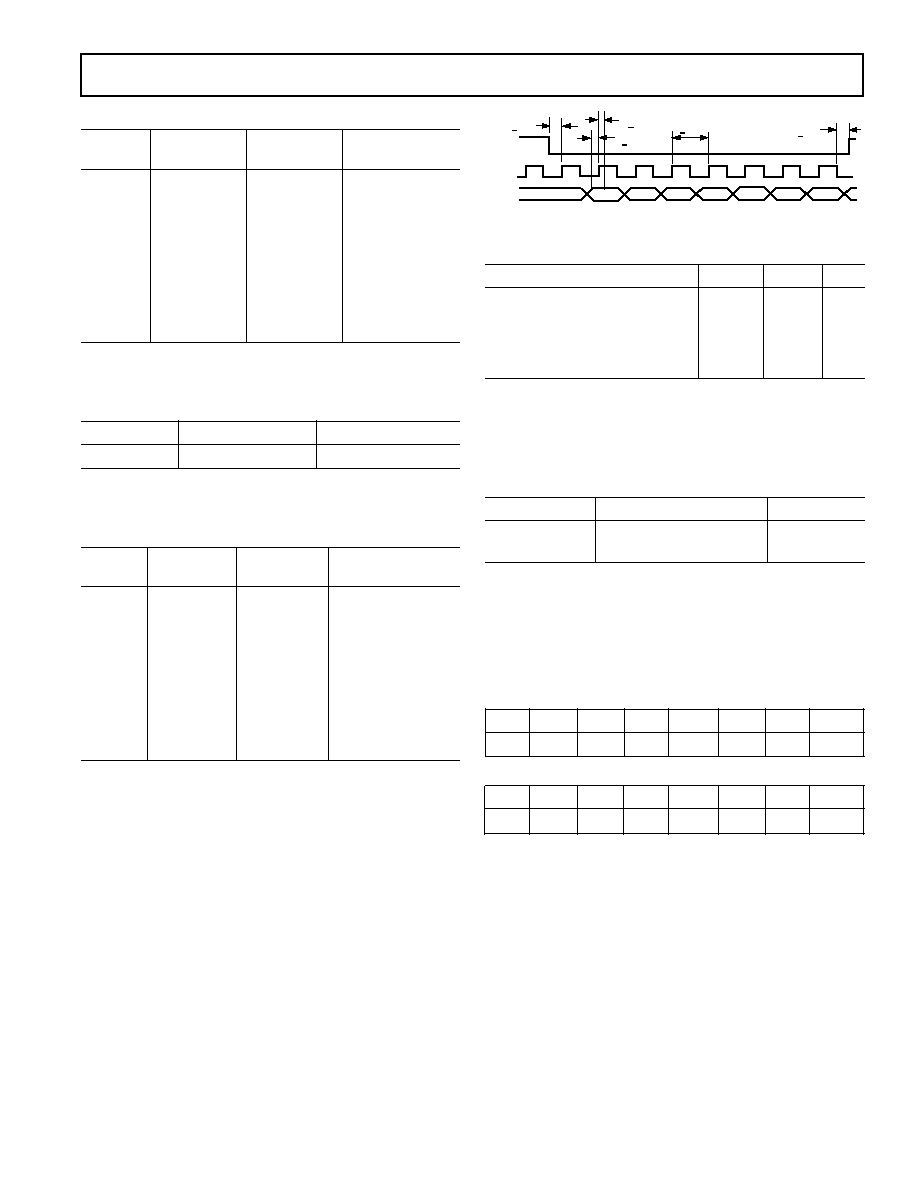
timing diagram for the serial interface.
t
HEN
t
DST
t
DHD
t
CLK
t
DEN
EN
CLK
DATA
MSB
LSB
Figure 3. Serial Interface Timing Diagram
Parameter
Symbol
Typ
Unit
Maximum Serial Clock Frequency
f_clk
13.824
MHz
Serial Data Set Up Time
t_dst
8
ns
Serial Data Hold Time
t_dhd
8
ns
Enable Set Up to Clock High
t_hen
10
ns
Clock Low to Enable Low
t_den
5
ns
The Least Significant Bit of the serial control word selects either
the "one-time setup" register or the operating mode register,
with the remaining 15 bits as data. Table II below details the
internal IC register mapping.
Table II. Register Mapping
Address (D0)
Function
Comments
0
One-Time IC Setup
See Table III
1
IC Operating Mode
See Table IV
AD6411 INITIAL SETUP
On power-up the state of the IC is not defined. A one-time setup
register must be loaded through the serial interface port, and is
selected when the LSB of the serial word is 0. After this one-
time setup, a single serial word controls operation of the IC.
Table III. One-Time IC Setup Register
D15
D14
D13
D12
D11
D10
D9
D8
X
RSB
TSB
SSB
RXM1 RXM0 TXM
BSWS
D7
D6
D5
D4
D3
D2
D1
D0
CF0
CT1
CT0
DSD
SFM
PDS
RD
0
AD6411
8
REV. 0
One-Time Setup Register Bit Definitions
RSB: Receive Control Line Sense Bit
RSB
Function
0
Receive Section POWER UP Active HIGH
1
Receive Section POWER UP Active LOW
TSB: Transmit Control Line Sense Bit
TSB
Function
0
Transmit Section POWER UP Active HIGH
1
Transmit Section POWER UP Active LOW
SSB: Synthesizer Control Line Sense Bit
SSB
Function
0
Synthesizer POWER UP Active LOW
1
Synthesizer POWER UP Active HIGH
RXM1, RXM0: Divider Power Mode In Active Receive Slot
RXM1
RXM0
Function
0
0
Dividers Powered Down, VCO Fly-
wheeled in Active Receive Mode
0
1
Dividers Powered Up, VCO Fly-
wheeled in Active Receive Mode
1
0
Dividers Powered Up, VCO Locked
to Synthesizer in Active Receive Mode
1
1
Dividers Powered Up, VCO Locked
to Synthesizer in Active Receive Mode
TXM: Divider Power Mode In Active Transmit Slot
TXM
Function
0
Dividers Powered Down, VCO Flywheeled in
Active Mode
1
Dividers Powered Up, VCO Flywheeled in Active
Mode
BSWS: Band Switch Sense (Control with External Lines)
BSWS
Function
0
Band Switch Output High in Receive Slot, PIN
Diode ON
1
Band Switch Output Low in Receive Slot, PIN
Diode ON
CF0: Configuration Bit 0
CF0
Function
0
Use Serial Interface for Mode Control
1
Use External Control Lines for Mode Control
CT1, CT0: Charge Pump Test Bits
CT1
CT0
Function
0
0
Three-State Output
0
1
Force Pump UP Current (Nom 1 mA)
1
0
Force Pump DOWN Current (Nom 1 mA)
1
1
Normal Operation (Driven from PFD)
DSD: Disable Data Slicer
DSD
Function
0
Disable On-Chip Data Slicer. Analog Output at Pin
DEMOD_DATA
1
Enable On-Chip Data Slicer. Digital Output at Pin
DEMOD_DATA
DSD bit is configured at power-up depending on whether an
external data slicer is being used in the system. Data slicer is
disabled when the IF strip is powered down irrespective of the
status of bit DSD.
SFM: S-Field Mode
SFM
Function
0
Normal Demodulation Mode
1
S-Field Sampling Mode
PDS: Phase Detector Sense
PDS
Function
0
PFD Pumps UP when Fvco > Fref
1
PFD Pumps UP when Fref > Fvco
RD: Reference Divide Ratio
RD
Function
0
Reference Frequency = 10.368 MHz
1
Reference Frequency = 13.824 MHz
AD6411
9
REV. 0
CONTROLLING THE AD6411 OPERATING MODE
Table IV. Operating Mode Control Register
D15
D14
D13
D12
D11
D10
D9
D8
M0
A4
A3
A2
A1
A0
IF/RSSI RXMixer
D7
D6
D5
D4
D3
D2
D1
D0
DMOD
DIV
CP
TX
UHF
BSW
REGS
1
BUF
VCO
The operating mode register, loaded through the serial port
when the LSB is "1," allows any circuit block to be indepen-
dently powered on or off. This can be bypassed to enable mode
control of the IC via the three external control lines. Transitions
between major DECT modes can be made with a single word
program (including channel change) when using the serial inter-
face only. Table V defines the bit status for the various IC oper-
ating modes when used with the serial interface only.
Table V. Bit Status for the Different Operating Modes
Data Bits
(D9 . . . D0)
Operating
Mode Register
Function
Comments
00 0000 0101
All Off Mode
All Circuits Off
00 0000 0111
Stand-By Mode
Regulators On
00 0111 1111
Prior to TX Slot
VCO, TX Buffer,
Dividers, Charge Pump,
Regulators Active,
VREF (1.4 V) Active
00 0101 1111
Active TX Slot
VCO, TX Buffer, Di-
viders, Regulator
Circuits Active,
VREF (1.4 V) Active
1
00 1110 1011
Prior to RX Slot
VCO
2
, Dividers, Charge
Pump, Regulators, De-
modulator Precharge
Circuits Active,
VREF (1.4 V) Active
11 1100 1011
Active RX Slot
RX Mixer, VCO
2
, Divid-
ers, Regulators, De-
modulator, Receive
Strip Circuits Active,
VREF (1.4 V) Active
NOTES
1
Alternatively it may be possible to power-down the dividers in an active trans-
mit slot depending on the effect of thermal transients on VCO pulling. In this
mode the dividers are biased but inactive. This can also be implemented when
external control lines are used with bits TXM, RXM1, RXM0.
2
Band switch output is determined by the status of BSW. Band switch output is
Low when BSW is high, high when BSW is low. In Table V, band switch
output is high for AcRx and PrRx slots, otherwise it is low.
CHANNEL SELECTION/FREQUENCY CONTROL
The M0 and A4A0 bits in the operating mode register control
the channel selection for the AD6411 synthesizer. The M0 bit
selects the M Counter division ratio.
M0: M Counter Divide Ratio
M0
Function
0
M Divide Ratio 32
1
M Divide Ratio 34
The A4 through A0 bits control the A counter division ratio,
and control the channel selection. Refer to the section of this
data sheet on Synthesizer Programming for a mapping of chan-
nel frequency to synthesizer divider words.
A4A0: A Counter Division Ratio
"A"
A4
A3
A2
A1
A0
0
0
0
0
0
0
1
0
0
0
0
1
2
0
0
0
1
0
3
0
0
0
1
1
30
1
1
1
1
0
31
1
1
1
1
1
ANALOG/RF INTERFACE DETAILS
The AD6411 is an advanced 1.9 GHz radio transceiver circuit
and requires careful attention to the selection of external com-
ponents. The AD6411 is readily capable of performance that
meets the ETS-300-176-1 (formerly TBR06) DECT radio
specifications. This section of the data sheet will describe sug-
gestions for external componentry that will allow the design of a
complete DECT RF transceiver.
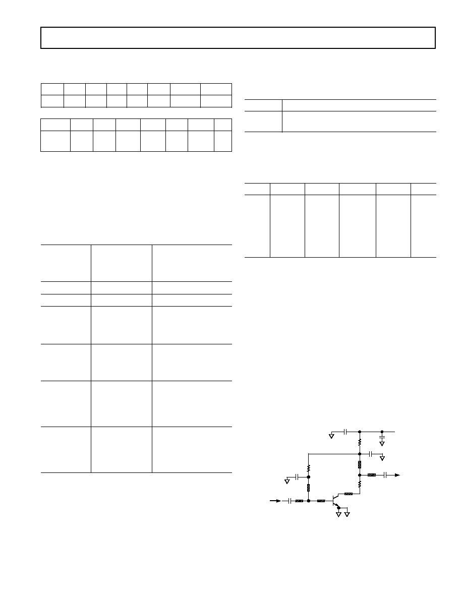
Low Noise Amplifier
An external LNA is required to meet the RF leakage specifica-
tions in ETS-300-176-1. The following circuit, based on a Si-
emens BFP405 discrete transistor, is representative of a suitable
LNA. The SC1.89 SAW filter removes images prior to the down
converter. The filter is matched to the AD6411 input with a
printed inductor and fixed capacitor. Complete details of the
circuit, with transmission-line dimensions, can be found in
Siemens Application Note No. 020.
RF IN
22pF
TL2
TL3
TL1
39k
100pF
100
TL6
10
BFP405
33pF
TL5
10pF
10nF
+3V
RF OUT
TL4
33pF
Figure 4. LNA circuit
AD6411
10
REV. 0
UHF VCO Tank Circuit
The UHF VCO is probably the most critical part of an AD6411-
based DECT radio. The design shown in Figure 5 uses a
printed inductor, a BBY53 (or equivalent) common-cathode
dual varactor, and a PIN-diode (BAR63-03W or equivalent)
band switch to cover the DECT band. The capacitance added
to the tank circuit by the PIN-diode is needed to switch the VCO
to the DECT receive band. It is switched out of the circuit in the
transmit mode, in which the VCO is directly modulated by
baseband transmit data. With this scheme, no manufacturing
trim is needed to tune the VCO to the DECT band. Tank com-
ponent values will need slight modification to cover the "ex-
tended DECT" frequency bands. The dimensions of tank
inductor L1 will depend on the circuit board material and thick-
ness used. Contact Analog Devices for assistance on UHF tank
inductor layout.
2pF
20k
20k
8.2pF
8.2pF
10k
BAR80
BAR63-03W
2k
L1
6.8pF
1nF
6.8k
2k
330pF
10k
10k
1.2pF
2pF
VCCVCO
VCOB
BSW
VCO
LF
AD6411
TX
DATA
IN
Figure 5. UHF VCO Circuit
Power Management
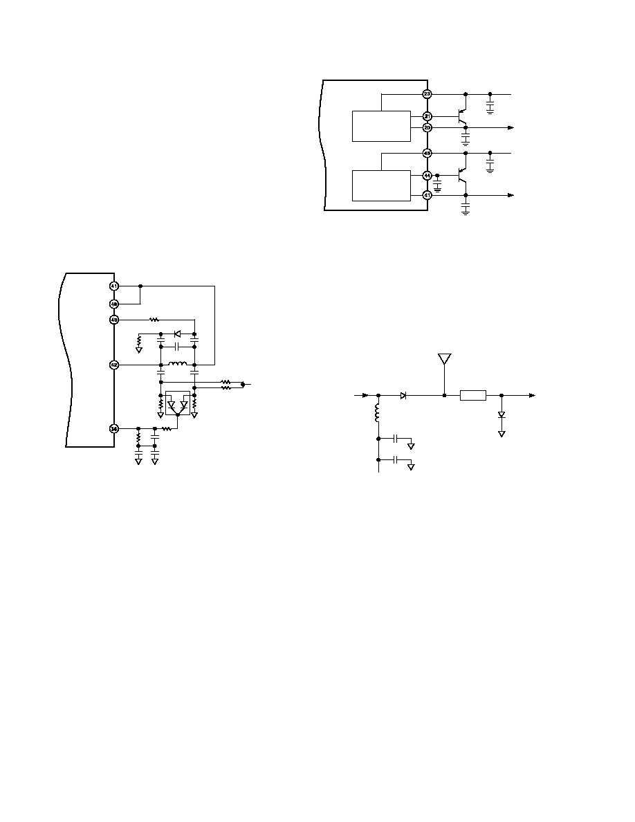
The AD6411 reduces the external components needed for
power management in a DECT radio by integrating voltage
regulators on-chip. The circuit can therefore operate directly
from a 3.0 V to 5.5 V unregulated battery supply.
There are two regulators. The first, VS1 (Pins 20, 21 and 23),
uses an external BCW68F (or similar) PNP pass transistor to
provide a regulated 2.75 V nominal supply voltage to most of
the AD6411 circuitry. The second regulator, VS2 (Pins 41, 44,
and 45), is intended to provide the regulated voltage to the
UHF VCO section and should not be used for other circuitry.
REGULATOR #1
REGULATOR #2
10nF
10nF
VBAT
VBAT
10nF
10pF
1nF
PASS TRANSISTORS: BCW68F OR EQUIVALENT
TO PIN 40 (VCOB)
AD6411
Figure 6. Voltage Regulator Circuitry
Transmit/Receive Switching
Since the same antenna is used for both transmit and receive, a
switch consisting of PIN diodes and printed transmission lines is
used to disconnect the receive path from the antenna during
transmit periods. A suggested circuit is shown in Figure 7.
Complete details can be found in Siemens Application Note
No. 007.
FROM PA
BAR63-03W
ANT
50
27nH
47pF
470pF
TX/RX
1=TX
0=RX
TO RX IN
BAR80
/4
Figure 7. T/R Switch
AD6411
11
REV. 0
48-Lead Plastic LQFP
(ST-48)
1
12
13
25
24
36
37
48
TOP VIEW
(PINS DOWN)
0.011 (0.27)
0.006 (0.17)
0.0197 (0.50)
TYP
0.217
(5.50)
BSC
SQ
0.362 (9.2)
0.346 (8.8)
SQ
0.280 (7.10)
0.272 (6.90)
SQ
SEATING
PLANE
0.063 (1.60) MAX
0.020 (0.52)
0.019 (0.48)
0.057 (1.45)
0.053 (1.35)
0.006 (0.15)
0.002 (0.05)
D
0.006 (0.15) MAX
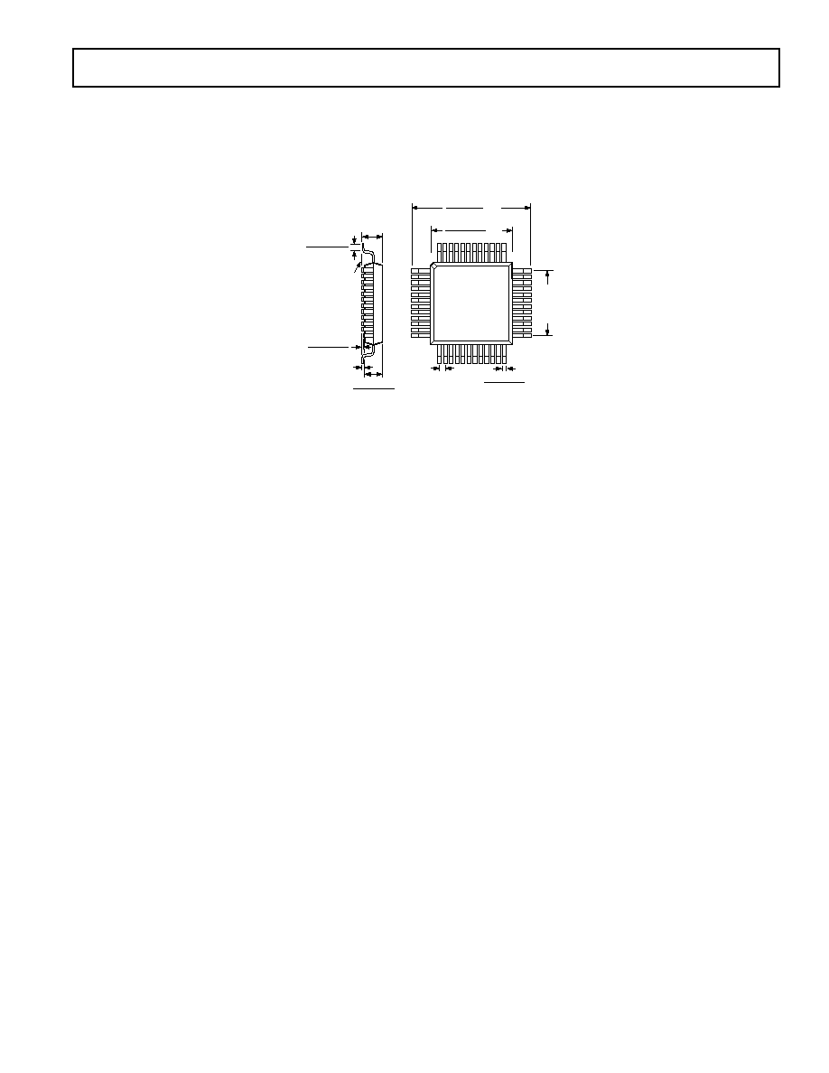
OUTLINE DIMENSIONS
Dimensions shown in inches and (mm).
C34052.59/98
PRINTED IN U.S.A.