 | ÐлекÑÑоннÑй компоненÑ: AD5582 | СкаÑаÑÑ:  PDF PDF  ZIP ZIP |
Äîêóìåíòàöèÿ è îïèñàíèÿ www.docs.chipfind.ru
PRELIMINARY TECHNICAL DATA
a
QUAD, Parallel-Input, Voltage Output,
12-/10-Bit Digital-to-Analog Converter
AD5582/AD5583
REV PrC, 23 APR '01
Information furnished by Analog Devices is believed to be accurate and reliable. However,
no responsibility is assumed by Analog Devices for its use; nor for any infringements of
patents or other rights of third parties which may result from its use. No license is granted
by implication or otherwise under any patent or patent rights of Analog Devices.
One Technology Way, P.O. Box 9106,
Norwood, MA 02062-9106 U
.
S
.
A
.
Tel: 781/329-4700 World Wide Web Site: http://www.analog.com
Fax:781/326-8703
©Analog Devices, Inc., 2000
FEATURES
12-Bit Linearity and Monotonic 40
o
C to +125
o
C
Single +5V to +12V or dual ±5V supply
Unipolar or Bipolar Operation
Double Buffered Registers Enable Simultaneous Multi-
Channels Update
4 Separate Rail-to Rail Reference Inputs
Parallel Interface
Data Readback Capability
5
µs Settling Time
APPLICATIONS
Process Control Equipment
Closed Loop Servo Control
Data Acquisition Systems
Digitally Controlled Calibration
Motor Control
Optical Network Control Loops
GENERAL DESCRIPTION
The AD5582/AD5583 family of quad, 12-/10-bit, voltage-output
digital-to-analog converter is designed to operate from a single +5
to +15 volt or a dual ±5V supply. Built using a CBCMOS process,
this monolithic DAC offers the user low cost, and ease-of-use in
single or dual-supply systems.
The applied external reference V
REF
determines the full-scale
output voltage. Valid V
REF
values include V
SS
<V
REF
<V
DD
resulting
in a wide selection of full scale outputs. For multiplying
applications AC inputs can be as large as |V
DD
-V
SS
|. Two on-board
precision trimmed resistors are available for 4-Quadrant
configurations.
A doubled-buffered parallel interface offers 25Mbps data load rates.
A common level-sensitive load-DAC strobe (
LDAC) input allows
simultaneous update of all DAC outputs from previously loaded
Input Registers. An external asynchronous reset (
RS) forces all
registers to the zero code state when MSB='0' or to midscale when
MSB='1'.
Both parts are offered in the same pin-out to allow users to select
the amount of resolution appropriate for their application without
circuit card redesign.
The AD5582/AD5583 are specified over the extended industrial
(-40°C to +125°C) temperature range. Packages available include
thin 1.1 mm TSSOP-48 package.
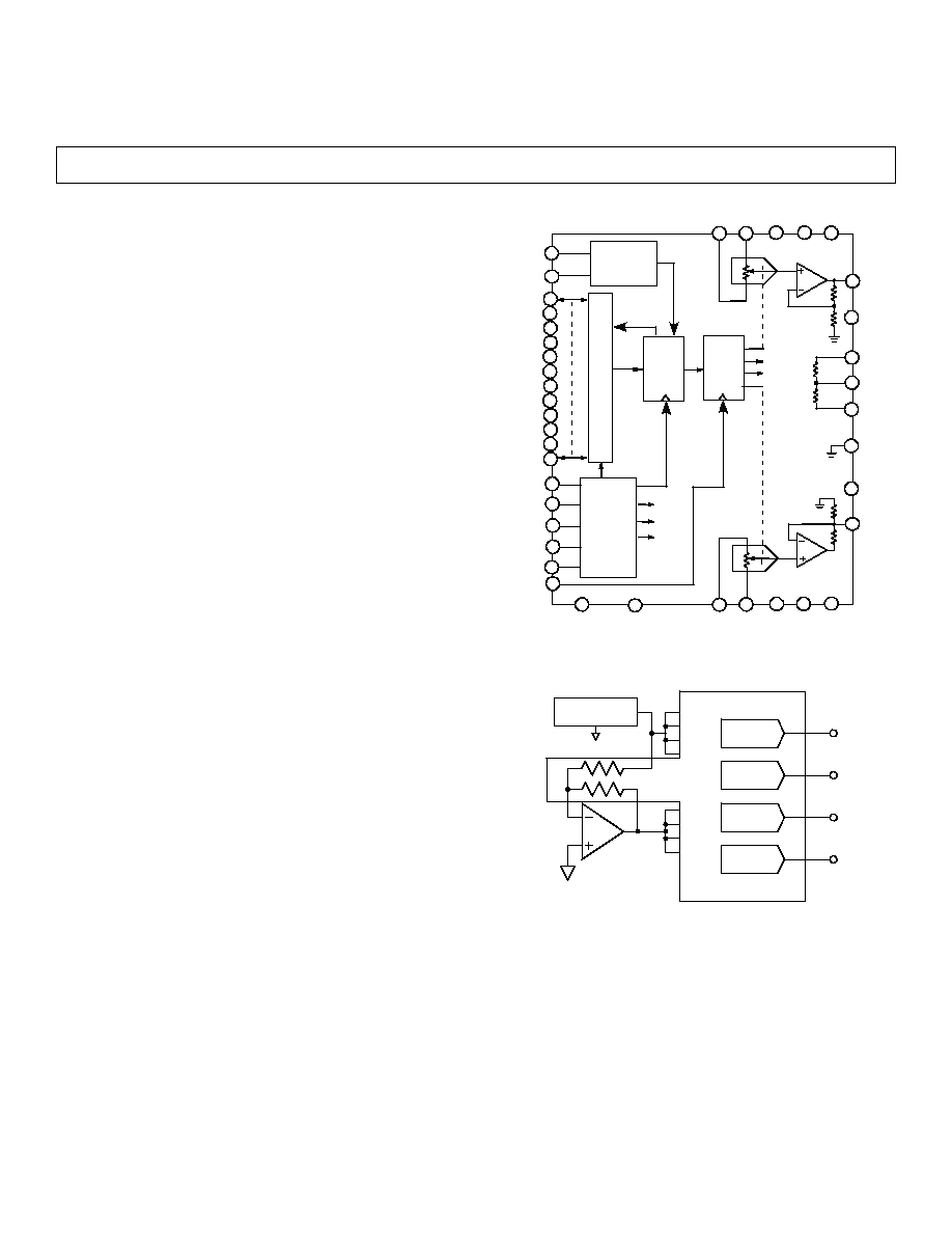
FUNCTIONAL DIAGRAM
11
23
13
12
6
7
V
OB
9
V
OC
3
4
5
20
V
OA
2
1
10
14
15
V
RLA
V
RHA
V
RLB
V
RHB
V
RHD
V
RLD
V
RHC
V
RLC
V
SS
V
DD
A GND
V
OD
IN
REG
I
N
T
E
R
F
A
C
E
OE
CONTROL
LOGIC
ADDR
DECODE
DAC
REG
27
24
25
26
31
28
29
30
35
32
33
34
DB11
DB10
DB9
DB8
DB7
DB6
DB5
DB4
DB3
DB2
DB1
DB0
CS
W/R
LDAC
DGND
VLOGIC
MSB
22
A1
A0
AD5582
36
37
21
17
19
16
Do
Di
18
RS
DVDD
RA
38
RB
RC
20k
20k
39
40
8
D A C A
D A C B
D A C C
D A C D
A D R 4 2 1
V
R E F L
A
B
C
D
V
R E F H
A
B
C
D
R
A
R
B
R
C
A D 5 5 8 2
D IG IT A L C IR C U IT R Y O M IT T E D F O R C L A R IT Y
+ 2 .5 V
-2 .5 V
±2 .5 V
±2 .5 V
±2 .5 V
±2 .5 V
Figure 1 Using Onboard Offset resistors to generate a negative
voltage REF

PRELIMINARY TECHNICAL DATA
AD5582/AD5583
This information applies to a product under development. Its characteristics and specifications are subject to change without notice. Analog Devices assumes no obligation regarding future
manufacture unless otherwise agreed to in writing.
REV PrC, 23 APR '01
2
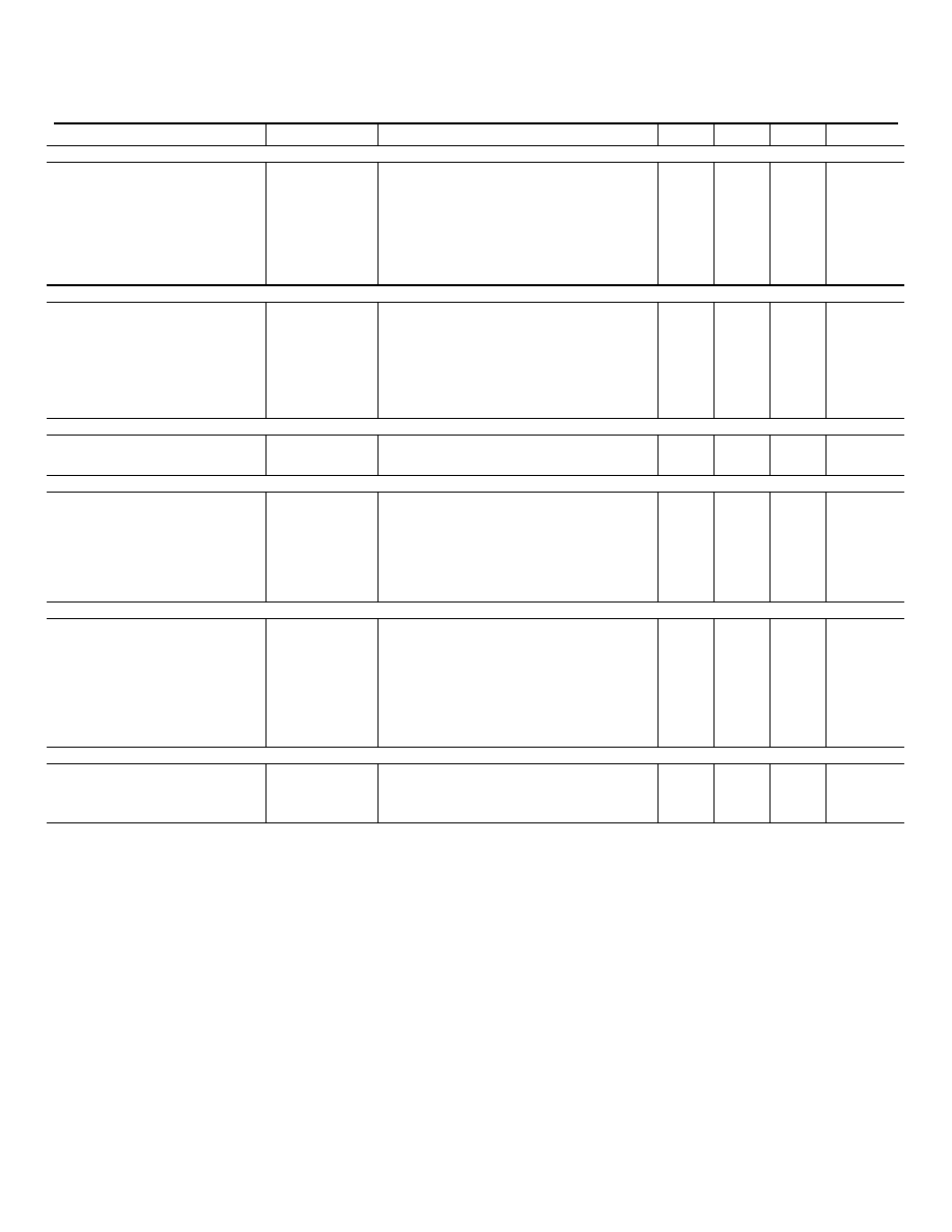
ELECTRICAL CHARACTERISTICS
at V
DD
=+5V, V
SS
= -5V, V
L
= +5V±10%, VREFH = +2.5V, VREFL = -2.5V, -40°C < TA < +125°C, unless otherwise noted.
PARAMETER
SYMBOL
CONDITION
MIN TYP MAX
UNITS
STATIC PERFORMANCE
Resolution
1
N AD5582
12 Bits
Resolution
1
N AD5583
10 Bits
Relative Accuracy
2
INL
-1
+1
LSB
Differential Nonlinearity
2
DNL Monotonic
-1 LSB
Zero-Scale Error
VZSE
Data = 000H
2 LSB
Full-Scale Voltage Error
VFSE
Data = FFFH
2 LSB
Full-Scale Tempco
3
TCVFS
10 ppm/
o
C
REFERENCE INPUT
VREFH Input Range
4
VREFH
V
SS
V
DD
V
VREFL Input Range
4
VREFL
V
SS
V
DD
V
Input Resistance
8
RREF
Data = 555
H
10
K
5
Input Capacitance
3
CREF
80 pF
REF Input Current
IREF
500
µA
REF Multiplying Bandwidth
BWREF
Hz
ANALOG OUTPUT
Output Current
IOUT
Data = 800H, VOUT = 4LSB
±2
mA
Capacitive Load
3
CL
No
Oscillation
500
pF
LOGIC INPUTS
Logic Input Low Voltage
VIL
V
L
= 5V ± 10%
0.8
V
Logic Input High Voltage
VIH
V
L
= 5V ± 10%
2.4
V
Input Leakage Current
IIL
µA
Input Capacitance
3
CIL
pF
Output Voltage High
V
OH
I
OH
= -0.8mA
2.4
V
Output Voltage Low
V
OL
I
OL
= 1.6mA
0.4
V
AC CHARACTERISTICS
Output Slew Rate
SR
Data = 000H to FFFH to 000H
2 V/
µs
Settling Time
7
tS
To ±0.1% of Full Scale
5
µs
Shutdown Recovery
t
SDR
µs
DAC Glitch
Q
Code 7FF
H
to 800
H
to 7FF
H
100 nVs
Digital Feed Through
VOUT/t
CS
Data=800
H
,
CS toggles at f=16MHz
5 nVs
Analog Crosstalk
VOUT/VREF
VREF = 1.5V
DC
+1VP-P, Data = 000H, f=100KHz
-80 dB
Output Noise
e
N
40 nV
Hz
SUPPLY CHARACTERISTICS
Positive Supply Current
IDD
VIL = 0V, No Load
3 mA
Negative Supply Current
ISS
VIL = 0V, No Load
3 mA
Power Dissipation
PDISS
VIL = 0V, No Load
30
mW
Power Supply Sensitivity
PSS
VDD = ±5%
30 ppm/V
NOTES:
1.
DAC Output Equation: V
OUT
= V
REFL
+ [(V
REFH
-V
REFL
)*Code/2^N], where Code = data loaded in corresponding DAC register A, B, C, D and N equals the
DAC resolution AD5582 = 12, AD5583 = 10 bits. One LSB = VREF/4096V for the 12-bit AD5582.
2.
The first two codes (000H, 001H) are excluded from the linearity error measurement in single supply operation.
3.
These parameters are guaranteed by design and not subject to production testing.
4. When
V
REF
is connected to either the V
DD
or the V
SS
power supply the corresponding V
OUT
voltage will program between ground and the supply voltage
minus the offset voltage of the output buffer, which is the same as the V
ZSE
error specification. See additional discussion in the operation section of the data
sheet.
5.
Typical specifications represent average readings measured at 25°C.
6.
The settling time specification does not apply for negative going transitions within the last 3 LSBs of ground in single supply operation.
PRELIMINARY TECHNICAL DATA
AD5582/AD5583
This information applies to a product under development. Its characteristics and specifications are subject to change without notice. Analog Devices assumes no obligation regarding future
manufacture unless otherwise agreed to in writing.
REV PrC, 23 APR '01
3
ELECTRICAL CHARACTERISTICS
at V
DD
=+15V, V
SS
= 0V, V
L
=+5V±10%, VREFH = +10V, VREFL = 0V, -40°C < TA < +125°C, unless otherwise noted.
PARAMETER
SYMBOL
CONDITION
MIN TYP MAX
UNITS
STATIC PERFORMANCE
Resolution
1
N AD5582
12 Bits
Resolution
1
N AD5583
10 Bits
Relative Accuracy
2
INL
-1
+1
LSB
Differential Nonlinearity
2
DNL Monotonic
-1 LSB
Zero-Scale Error
VZSE
Data = 000H
2 LSB
Full-Scale Voltage Error
VFSE
Data = FFFH
2 LSB
Full-Scale Tempco
3
TCVFS
10 ppm/
o
C
REFERENCE INPUT
VREFH Input Range
4
VREFH
V
SS
V
DD
V
VREFL Input Range
4
VREFL
0
V
DD
V
Input Resistance
8
RREF
Data = 555
H
10
K
5
Input Capacitance
3
CREF
80 pF
REF Input Current
IREF
500
µA
REF Multiplying Bandwidth
BWREF
Hz
ANALOG OUTPUT
Output Current
IOUT
Data = 800H, VOUT = 4LSB
+5
mA
Capacitive Load
3
CL
No
Oscillation
500
pF
LOGIC INPUTS/OUTPUTS
Logic Input Low Voltage
VIL
0.8
V
Logic Input High Voltage
VIH
2.4
V
Input Leakage Current
IIL
µA
Input Capacitance
3
CIL
pF
Output Voltage High
V
OH
I
OH
= -0.8mA
2.4
V
Output Voltage Low
V
OL
I
OL
= 1.6mA
0.4
V
AC CHARACTERISTICS
Output Slew Rate
SR
Data = 000H to FFFH to 000H
2 V/
µs
Settling Time
7
tS
To ±0.1% of Full Scale
5
µs
Shutdown Recovery
t
SDR
µs
DAC Glitch
Q
Code 7FF
H
to 800
H
to 7FF
H
100 nVs
Digital Feed Through
VOUT/t
CS
Data=800
H
,
CS toggles at f=16MHz
5 nVs
Analog Crosstalk
VOUT/VREF
VREFH = 2.5V
DC
+1VP-P, Data = 000H, f=100KHz
-80 dB
Output Noise
e
N
40 nV
Hz
SUPPLY CHARACTERISTICS
Positive Supply Current
IDD
VIL = 0V, No Load
3 mA
Power Dissipation
PDISS
VIL = 0V, No Load
45
mW
Power Supply Sensitivity
PSS
VDD = ±5%
30 ppm/V
NOTES:
1.
DAC Output Equation: V
OUT
= V
REFL
+ [(V
REFH
-V
REFL
)*Code/2^N], where Code = data loaded in corresponding DAC register A, B, C, D and N equals the
DAC resolution AD5582 = 12, AD5583 = 10 bits. One LSB = VREF/4096V for the 12-bit AD5582.
2.
The first two codes (000H, 001H) are excluded from the linearity error measurement in single supply operation.
3.
These parameters are guaranteed by design and not subject to production testing.
4. When
V
REF
is connected to either the V
DD
or the V
SS
power supply the corresponding V
OUT
voltage will program between ground and the supply voltage
minus the offset voltage of the output buffer, which is the same as the V
ZSE
error specification. See additional discussion in the operation section of the data
sheet.
5.
Typical specifications represent average readings measured at 25°C.
6.
The settling time specification does not apply for negative going transitions within the last 3 LSBs of ground in single supply operation.
PRELIMINARY TECHNICAL DATA
AD5582/AD5583
This information applies to a product under development. Its characteristics and specifications are subject to change without notice. Analog Devices assumes no obligation regarding future
manufacture unless otherwise agreed to in writing.
REV PrC, 23 APR '01
4
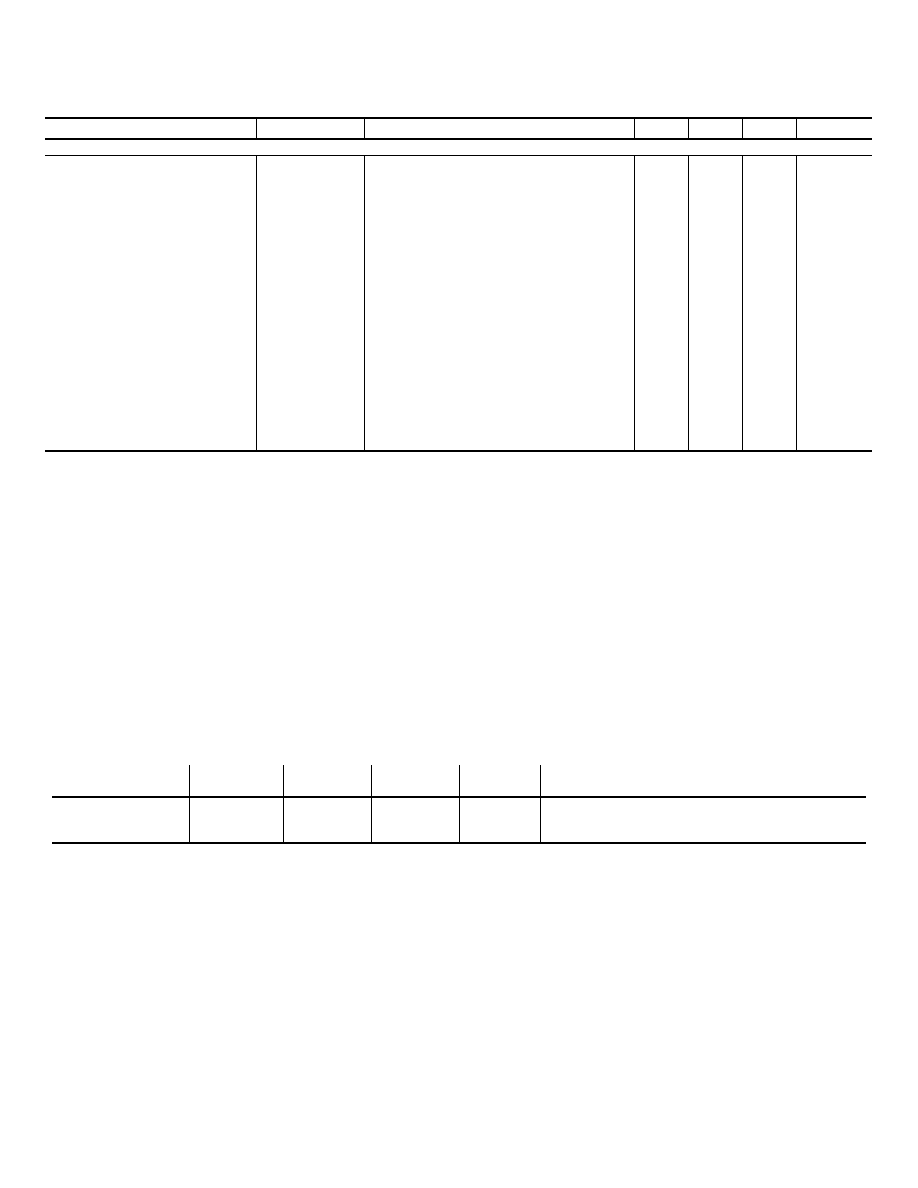
ELECTRICAL CHARACTERISTICS
at V
DD
=+15V, V
SS
= 0V, V
L
=+5V±10%, VREFH = +10V, VREFL = 0V, -40°C < TA < +125°C, unless otherwise noted.
PARAMETER
SYMBOL
CONDITION
MIN TYP MAX
UNITS
INTERFACE TIMING
1,2
Clock Frequency
f
CLK
25
MHz
Chip Select Write Pulsewidth
t
WCS
30 ns
Write Setup
t
WS
t
WCS
= 50 ns
0
ns
Write Hold
t
WH
t
WCS
= 50 ns
0
ns
Address Setup
t
AS
0 ns
Address Hold
t
AH
0 ns
Load Setup
t
LS
70
ns
Load Hold
t
LH
30
ns
Write Data Setup
t
WDS
t
WCS
= 50 ns
0
ns
Write Data Hold
t
WDH
t
WCS
= 50 ns
0
ns
Load Data Pulsewidth
t
LDW
50 ns
Reset Pulsewidth
t
RESET
50 ns
Chip Select Read Pulsewidth
t
RCS
130
ns
Read Data Hold
t
RDH
t
RCS
= 130 ns
0
ns
Read Data Setup
t
RDS
t
RCS
= 130 ns
0
ns
Data to Hi Z
t
DZ
C
L
= 10pF
100
ns
Chip Select to Data
t
CSD
C
L
= 100pF
100
ns
Chip Select Repetitive Pulsewidth
t
CSP
10 ns
Load Setup in Double Buffer Mode
t
LDS
20 ns
NOTES:
1.
All input control signals are specified with t
R
= t
F
= 2ns (10% to 90% of +3V) and timed from a voltage level of 1.5V.
2.
Typicals represent average readings measured at 25°C.
ABSOLUTE MAXIMUM RATINGS
VDD to VSS.......................................................-0.3V to +16.5V
VDD to GND..........................................................-0.3V to 5.5V
VSS to GND.........................................................+0.3V to -5.5V
VDD to VREF+............................................. -0.3V to (V
DD
-V
SS
)
VREF- to VSS ............................................... -0.3V to (V
DD
-V
SS
)
VREFH to VREFL ........................................ -0.3V to (V
DD
-V
SS
)
Logic Inputs to GND ............................ V
SS
0.3V, VDD + 0.3V
V
OUT
to GND ....................................... V
SS
0.3V, VDD + 0.3V
I
OUT
Short Circuit to GND ...........................................................
Thermal Resistance
JA
TSSOP-48 Lead (RU-48) ........................................ xxx°C/W
Maximum Junction Temperature (T
J
MAX
) ........................ 150°C
Package Power Dissipation = (TJ MAX TA)/JA
Operating Temperature Range ..........................40°C to +125°C
Storage Temperature Range ..............................65°C to +150°C
Lead Temperature:
RU-48 (Vapor Phase, 60 secs)...................................... xxx°C
RU-44 (Infrared, 15 secs) ............................................. xxx°C
Stress above those listed under "Absolute Maximum Ratings" may cause permanent damage to
the device. This is a stress rating only and functional operation of the device at these or any other
conditions above those indicated in the operational sections of this specification is not implied.
Exposure to absolute maximum rating conditions for extended periods may affect device reliability.
ORDERING GUIDE:
Resolution
TEMP
Package
Package
Container
MODEL (Bits)
RANGE
Description
Option
Qty
AD5582YRU-REEL7 12 -40/+125°C
TSSOP-48
RU-48
AD5583YRU-REEL7 10 -40/+125°C
TSSOP-48
RU-48
The AD5582 contains xxx transistors. The die size measures 108 mil X 144 mil.
PRELIMINARY TECHNICAL DATA
AD5582/AD5583
This information applies to a product under development. Its characteristics and specifications are subject to change without notice. Analog Devices assumes no obligation regarding future
manufacture unless otherwise agreed to in writing.
REV PrC, 23 APR '01
5
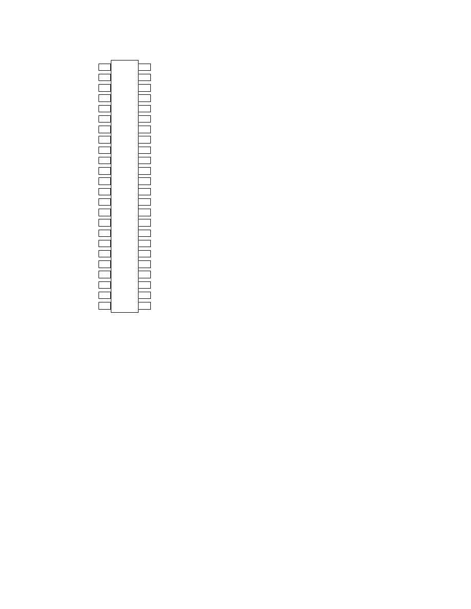
PIN CONFIGURATION
1
2
3
4
5
6
7
8
9
1 0
1 1
1 2
1 3
1 4
1 5
1 6
1 7
1 8
1 9
2 0
2 1
2 2
2 3
2 4
4 8
4 7
4 6
4 5
4 4
4 3
4 2
4 1
4 0
3 9
3 8
3 7
3 6
3 5
3 4
3 3
3 2
3 1
3 0
2 9
2 8
2 7
2 6
2 5
NOTE: Pin Out not finalized!
Please contact Analog Devices Inc. for final version
Pin# Name
Description
.
VRLA
Voltage Reference Low Input Terminal DAC A
VRHA
Voltage Reference High Input Terminal DAC A
VRLB
Voltage Reference Low Input Terminal DAC B
VRHB
Voltage Reference High Input Terminal DAC B
VDD
Positive Power Supply
VOA
DAC A Output
VOB
DAC B output
RA
End Tap Offset Resistor
RB
Center Tap Offset Resistor
RC
End Tap Offset Resistor
AGND
Analog
Ground
VOC
Voltage Out DAC C
VOD
DAC D Output
VSS
Negative Power Supply
VRLC
Voltage Reference Low Input Terminal DAC C
VRHC
Voltage Reference High Input Terminal DAC C
VRLD
Voltage Reference Low Input Terminal DAC D
VRHD
Voltage Reference High Input Terminal DAC D
DGND
Digital
Ground
DVDD
LDAC
DAC Register Load, active low level sensitive
RS Reset
strobe
MSB
Reset Mode: MSB=0 Code = 000
H
, MSB=1 Code
800
H
VL
Logic Supply Voltage
W/R
Write Read Mode select
CS
Chip Select, active low
DB0
Data Bit 0
DB1
Data Bit 1
DB2
Data Bit 2
DB3
Data Bit 3
DB4
Data Bit 4
DB5
Data Bit 5
DB6
Data Bit 6
DB7
Data Bit 7
DB8
Data Bit 8
DB9
Data Bit 9
DB10
Data Bit 10
DB11
Data Bit 11
A0 Address
Input
0
A1 Address
Input
1
Document Outline
- Specifications
- Pinout
- Package drawings
- Ordering Guide
- Features
- Applications
- Product Description
- Absolute Maximum Ratings
- STATIC PERFORMANCE
- REFERENCE INPUT
- ANALOG OUTPUT
- LOGIC INPUTS
- AC CHARACTERISTICS
- SUPPLY CHARACTERISTICS
- STATIC PERFORMANCE
- REFERENCE INPUT
- ANALOG OUTPUT
- LOGIC INPUTS/OUTPUTS
- AC CHARACTERISTICS
- SUPPLY CHARACTERISTICS
- INTERFACE TIMING
- DIAGRAMS
- Using Onboard Offset resistors to generate a negative voltage REF
- DATA OUTPUT (READ TIMING)
- DATA WRITE (INPUT AND OUTPUT REGISTERS) TIMING
- SINGLE BUFFER MODE (OUTPUT UPDATED INDIVIDUALLY)
- DOUBLE BUFFER MODE (OUTPUT UPDATED SIMULTANEOUSLY)