 | ÐлекÑÑоннÑй компоненÑ: AD53033 | СкаÑаÑÑ:  PDF PDF  ZIP ZIP |
Äîêóìåíòàöèÿ è îïèñàíèÿ www.docs.chipfind.ru
REV. 0
Information furnished by Analog Devices is believed to be accurate and
reliable. However, no responsibility is assumed by Analog Devices for its
use, nor for any infringements of patents or other rights of third parties
which may result from its use. No license is granted by implication or
otherwise under any patent or patent rights of Analog Devices.
a
AD53033
One Technology Way, P.O. Box 9106, Norwood, MA 02062-9106, U.S.A.
Tel: 781/329-4700
World Wide Web Site: http://www.analog.com
Fax: 781/326-8703
© Analog Devices, Inc., 1999
High Performance Driver/Comparator
on a Single Chip
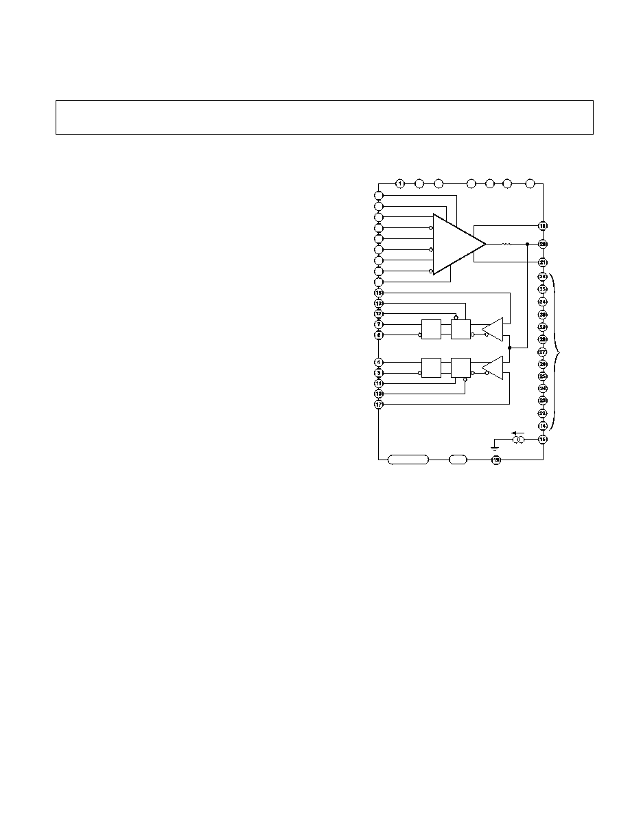
FUNCTIONAL BLOCK DIAGRAM
DRIVER
COMPARATOR
50
1.0 A/K
V
CC
V
CC
V
CC
V
EE
V
EE
V
EE
V
EE
51
52
39
40
41
32
AD53033
V
OUT
VLDCPL
2, 5, 8
9, 33, 44, 46, 48
PWRGND
ECLGND
HQGND2
THERM
31
50
49
42
43
38
37
45
47
VH
VTERM
DATA
IOD
RLD
V
L
HCOMP
LEH
QH
QHB
QL
LEL
LCOMP
NC = NO CONNECT
DATAB
IODB
RLDB
LEHB
QLB
LELB
NC
VHDCPL
FEATURES
250 MHz Operation
Driver/Comparator Included
52-Lead LQFP Package with Built-in Heat Sink
APPLICATIONS
Automatic Test Equipment
Semiconductor Test Systems
Board Test Systems
Instrumentation and Characterization Equipment
PRODUCT DESCRIPTION
The AD53033 is a single chip that performs the pin electronics
functions of driver and comparator (D-C) in ATE VLSI and
memory testers.
The driver is a proprietary design that features three active
states: Data High Mode, Data Low Mode and Term Mode as
well as an Inhibit State. This facilitates the implementation of
high speed active termination. The output voltage range is 3 V
to +8 V to accommodate a wide variety of test devices. The
output leakage is typically less than 250 nA over the entire sig-
nal range.
The dual comparator, with an input range equal to the driver
output range, features built-in latches and ECL-compatible
outputs. The outputs are capable of driving 50
signal lines
terminated to 2 V. Signal tracking capability is upwards of
5 V/ns.
Also included on the chip is an onboard temperature sensor
whose purpose is to give an indication of the surface tempera-
ture of the D-C. This information can be used to measure
JC
and
JA
or flag an alarm if proper cooling is lost. Output from the
sensor is a current sink that is proportional to absolute tempera-
ture. The gain is trimmed to a nominal value of 1.0
µ
A/K. As
an example, the output current can be sensed by using a 10 k
resistor connected from +10 V to the THERM (IOUT) pin. A
voltage drop across the resistor will be developed that equals:
10K
×
1
µ
A/K = 10 mV/K = 2.98 V at room temperature.

2
REV. 0
AD53033SPECIFICATIONS
DRIVER SPECIFICATIONS
(All specifications are at T
J
= +85 C
5 C, +V
S
= +12 V
3%, V
S
= 7 V = 3% unless otherwise noted. All temperature coefficients are
measured at T
J
= +75 C to +95 C). CHDCPL = CLDCPL = 39 nF.
Parameter
Min
Typ
Max
Units
Test Conditions
DIFFERENTIAL INPUT CHARACTERISTICS
(DATA to DATA, IOD to IOD, RLD to RLD)
Input Voltage
2
0
V
Differential Input Range
ECL
Bias Current
250
+250
µ
A
V
IN
= 2 V, 0.0 V
REFERENCE INPUTS
Bias Currents
50
+50
µ
A
V
L
, V
H
, V
T
= 5 V
OUTPUT CHARACTERISTICS
Logic High Range
2
8
V
DATA = H, V
H
= 2 V to +8 V
V
L
= 3 V (V
H
= 2 V to +6 V)
V
L
= 1 V (V
H
= +6 V to +8 V)
Logic Low Range
3
5
V
DATA = L, V
L
= 3 V to +5 V, V
H
= +6 V
Amplitude (V
H
and V
L
)
0.1
9
V
V
L
= 0.0 V, V
H
= +0.1 V, V
T
= 0 V
Absolute Accuracy
V
L
= 2 V, V
H
= +7 V, V
T
= 0 V
V
H
Offset
50
+50
mV
DATA = H, V
H
= 0 V, V
L
= 3 V, V
T
= +3 V
V
H
Gain + Linearity Error
0.3 5
+0.3 + 5
% of V
H
+ mV
DATA = H, V
H
= 2 V to +8 V, V
L
= 3 V, V
T
= +3 V
V
L
Offset
50
+50
mV
DATA = L, V
L
= 3 V, V
H
= +6 V, V
T
= +7.5 V
V
L
Gain + Linearity Error
0.3 5
+0.3 + 5
% of V
L
+ mV
DATA = L, V
L
= 0 V , V
H
= +6 V, V
T
= +7.5 V
Offset TC
0.5
mV/
°
C
V
L
= 0 V, V
H
= +5 V, V
T
= 0 V
Output Resistance
V
H
= 2 V
44
46
48
V
L
= 3 V, V
T
= 0 V, I
OUT
= 0, +1, +30 mA
V
H
= +8 V
44
46
48
V
L
= 1 V, V
T
= 0 V, I
OUT
= 0, 1, 30 mA
V
L
= 3 V
44
46
48
V
H
= +6 V, V
T
= 0 V, I
OUT
= 0, +1, +30 mA
V
L
= +5 V
44
46
48
V
H
= +6 V, V
T
= 0 V, I
OUT
= 0, 1, 30 mA
V
H
= +3 V
46
V
L
= 0 V, V
T
= 0 V, I
OUT
= 30 mA (Trim Point)
Dynamic Current Limit
100
mA
C
BYP
= 39 nF, V
H
= +7 V, V
L
= 2 V, V
T
= 0 V
Static Current Limit
85
+85
mA
Output to 3 V, V
H
= +8 V, V
L
= 1 V, V
T
= 0 V
DATA = H and Output to +8 V, V
H
= +6 V,
V
L
= 3 V, V
T
= 0 V, DATA = L
V
TERM
Voltage Range
3
8.0
V
TERM MODE, V
T
= 3 V to +8 V, V
L
= 0 V, V
H
= 3 V
V
TERM
Offset
50
+50
mV
TERM MODE, V
T
= 0 V, V
L
= 0 V, V
H
= 3 V
V
TERM
Gain + Linearity Error
0.3 + 5
+0.3 + 5
% of V
SET
+ mV
TERM MODE, V
T
= 3 V to +8 V, V
L
= 0 V, V
H
= 3 V
Offset TC
0.5
mV/
°
C
V
T
= 0 V, V
L
= 0 V, V
H
= 3 V
Output Resistance
44
46
49
I
OUT
= +30 mA, +1.0 mA, V
T
= 3.0 V, V
H
= 3 V, V
L
= 0 V
I
OUT
= 30 mA, 1.0 mA, V
T
= +8.0 V, V
H
= 3 V, V
L
= 0 V
I
OUT
=
±
30 mA,
±
1.0 mA, V
T
= 0 V, V
H
= 3 V, V
L
= 0 V
DYNAMIC PERFORMANCE, (V
H
AND V
L
)
Propagation Delay Time
1.1
1.6
2.1
ns
Measured at 50%, V
H
= +400 mV, V
L
= 400 mV
Propagation Delay TC
2
ps/
°
C
Measured at 50%, V
H
= +400 mV, V
L
= 400 mV
Delay Matching, Edge to Edge
<100
ps
Measured at 50%, V
H
= +400 mV, V
L
= 400 mV
Rise and Fall Times
1 V Swing
0.6
ns
Measured 20%80%, V
L
= 0 V, V
H
= 1 V
3 V Swing
1.0
ns
Measured 20%80%, V
L
= 0 V, V
H
= 3 V
5 V Swing
1.7
ns
Measured 10%90%, V
L
= 0 V, V
H
= 5 V
9 V Swing
3.0
ns
Measured 10%90%, V
L
= 2 V, V
H
= 7 V
Rise and Fall Time Temperature Coefficient
1 V Swing
±
1
ps/
°
C
Measured 20%80%, V
L
= 0 V, V
H
= 1 V
3 V Swing
±
2
ps/
°
C
Measured 20%80%, V
L
= 0 V, V
H
= 3 V
5 V Swing
±
4
ps/
°
C
Measured 10%90%, V
L
= 0 V, V
H
= 5 V
Overshoot and Preshoot
3.0 50
+3.0 + 50
% of Step + mV
V
L
, V
H
= 0.1 V, 0.1 V, V
L
, V
H
= 0.0 V, 1.0 V
V
L
, V
H
= 0.0 V, 3.0 V, V
L
, V
H
= 0.0 V, 5.0 V
V
L
, V
H
= 2.0 V, 7.0 V
Settling Time
to 15 mV
<50
ns
V
L
= 0 V, V
H
= 0.5 V
to 4 mV
<10
µ
s
V
L
= 0 V, V
H
= 0.5 V

3
REV. 0
AD53033
Parameter
Min
Typ
Max
Units
Test Conditions
Delay Change vs. Pulsewidth
<50
ps
V
L
= 0 V, V
H
= 2 V
Minimum Pulsewidth
3 V Swing
2
ns
V
L
= 0 V, V
H
= 3 V, 90% Reached, Measure @ 50%
5 V Swing
3
ns
V
L
= 0 V, V
H
= 5 V, 90% Reached, Measure @ 50%
Toggle Rate
250
MHz
V
L
= 0 V, V
H
= 5 V, VDUT > 3.0 V p-p
DYNAMIC PERFORMANCE, INHIBIT
Delay Time, Active to Inhibit
1.5
4.0
ns
Measured at 50%, V
H
= +2 V, V
L
= 2 V
Delay Time, Inhibit to Active
1.5
3.5
ns
Measured at 50%, V
H
= +2 V, V
L
= 2 V
Delay Time Matching (Z)
±
2.2
ns
Z = Delay Time Active to Inhibit Test (Above)--
Delay Time Inhibit to Active Test (Above)
(Of Worst Two Edges)
I/O Spike
<200
mV, p-p
V
H
= 0 V, V
L
= 0 V
Rise, Fall Time, Active to Inhibit
3.5
ns
V
H
= +2 V, V
L
= 2 V (Measured 20%/80% of 1 V Output)
Rise, Fall Time, Inhibit to Active
2.2
ns
V
H
= +2 V, V
L
= 2 V (Measured 20%/80% of 1 V Output)
DYNAMIC PERFORMANCE , V
TERM
Delay Time, V
H
to V
TERM
3.0
ns
Measured at 50%, V
L
= V
H
= +0.4 V, V
TERM
= 0.4 V
Delay Time, V
L
to V
TERM
5.0
ns
Measured at 50%, V
L
= V
H
= +0.4 V, V
TERM
= 0.4 V
Delay Time, V
TERM
to V
H
and V
TERM
to V
L
4.0
ns
Measured at 50%, V
L
= V
H
= +0.4 V, V
TERM
= 0.4 V
Overshoot and Preshoot
3.0 + 75
+3.0 + 75
% of Step + mV
V
H
/V
L
, V
TERM
= (+0.4 V, 0.4 V), (0.0 V, 2.0 V),
(0.0 V, +7.0 V)
V
TERM
Mode Rise Time
4.0
ns
V
L
, V
H
= 0 V, V
TERM
= 2 V, 20%80%
V
TERM
Mode Fall Time
5.5
ns
V
L
, V
H
= 0 V, V
TERM
= 2 V, 20%80%
PSRR, DRIVE or TERM Mode
35
dB
V
S
= V
S
±
3%
Specifications subject to change without notice.
COMPARATOR SPECIFICATIONS
(All specifications are at T
J
= +85 C
5 C, +V
S
= +12 V
3%, V
S
= 7 V = 3% unless otherwise noted. All temperature coefficients are
measured at T
J
= +75 C to +95 C).
Parameter
Min
Typ
Max
Units
Test Conditions
DC INPUT CHARACTERISTICS
Offset Voltage (V
OS
)
25
25
mV
CMV = 0 V
Offset Voltage (Drift)
50
µ
V/
°
C
CMV = 0 V
HCOMP, LCOMP Bias Current
50
50
µ
A
V
IN
= 0 V
Voltage Range (V
CM
)
3
8.0
V
Differential Voltage (V
DIFF
)
9.0
V
Gain and Linearity
0.05
0.05
% FSR
V
IN
= 3 V to +8 V
LATCH ENABLE INPUTS
Logic "1" Current (I
IH
)
250
µ
A
LE, LE = 0.8 V
Logic "0" Current (I
IL
)
250
µ
A
LE, LE = 1.8 V
DIGITAL OUTPUTS
Logic "1" Voltage (V
OH
)
0.98
V
Q or Q, 50
to 2 V
Logic "0" Voltage (V
OL
)
1.5
V
Q or Q, 50
to 2 V
Slew Rate
1
V/ns
SWITCHING PERFORMANCE
Propagation Delay
Input to Output
0.9
2.5
ns
V
IN
= 2 V p-p,
Latch Enable to Output
2
ns
HCOMP = +1 V, LCOMP = +1 V
Propagation Delay Temperature Coefficient
2
ps/
°
C
Propagation Delay Change with Respect to
Slew Rate: 0.5 V, 1.0 V, 3.0 V/ns
<
±
100
ps
V
IN
= 0 V to 5 V
Slew Rate: 5.0 V/ns
<
±
350
ps
V
IN
= 0 V to 5 V
Amplitude: 1.0 V, 3.0 V, 5.0 V
<
±
200
ps
V
IN
= 1.0 V/ns
Equivalent Input Rise Time
450
ps
V
IN
= 0 V to 3 V, 3 V/ns
Pulsewidth Linearity
<
±
200
ps
V
IN
= 0 V to 3 V, 3 V/ns, PW = 3 ns8 ns
Settling Time
<25
ns
Settling to
±
8 mV, V
IN
= 1 V to 0 V
Latch Timing
Input Pulsewidth
<1.5
ns
Setup Time
<1.0
ns
Hold Time
<1.0
ns
Specifications subject to change without notice.
4
REV. 0
AD53033SPECIFICATIONS
TOTAL FUNCTION SPECIFICATIONS
(All specifications are at T
J
= +85 C
5 C, +V
S
= +12 V
3%, V
S
= 7 V = 3% unless otherwise noted. All temperature coefficients are
measured at T
J
= +75 C to +95 C).
Parameter
Min
Typ
Max
Units
Test Conditions
OUTPUT CHARACTERISTICS
Output Leakage Current, V
OUT
= 2 V to +7 V
500
+500
nA
Output Leakage Current, V
OUT
= 3 V to +8 V
2
+2
µ
A
Output Capacitance
6
pF
Driver INHIBITED
POWER SUPPLIES
Total Supply Range
19
V
Positive Supply
12
V
Negative Supply
7
V
Positive Supply Current
178
mA
Driver = Active
Negative Supply Current
195
mA
Driver = Active
Total Power Dissipation
3.5
W
Driver = Active
Temperature Sensor Gain Factor
0.7
1
1.4
µ
A/K
R
LOAD
= 10 k
, V
SOURCE
= +10 V
NOTES
Connecting or shorting the decoupling pins to ground will result in the destruction of the device.
Specifications subject to change without notice.
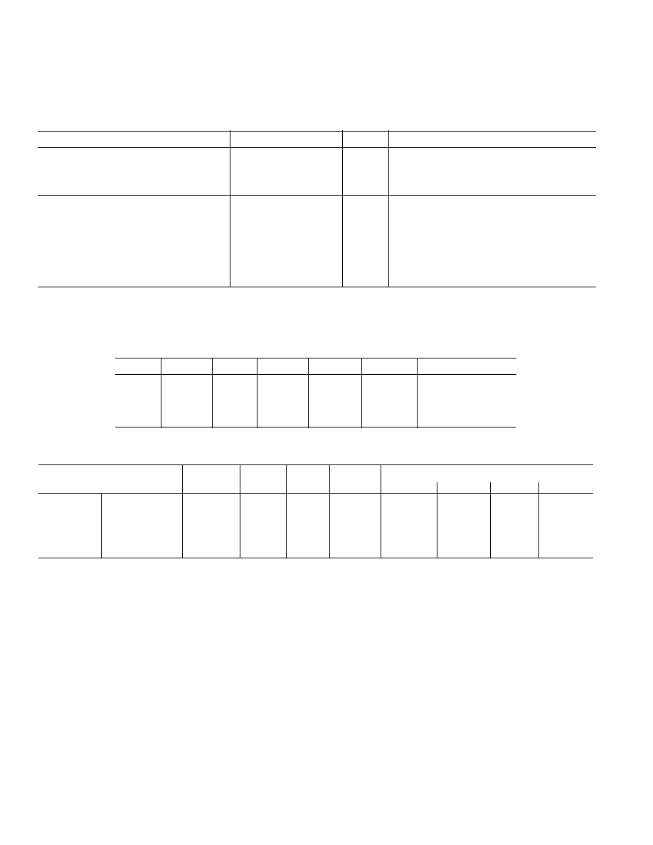
Table I. Driver Truth Table
DATA
DATA
IOD
IOD
RLD
RLD
OUTPUT STATE
0
1
1
0
X
X
VL
1
0
1
0
X
X
VH
X
X
0
1
0
1
INH
X
X
0
1
1
0
VTERM
Table II. Comparator Truth Table
OUTPUT STATES
V
OUT
LEH
LEH
LEL
LEL
QH
QH
QL
QL
>HCOMP
>LCOMP
1
0
1
0
1
0
1
0
>HCOMP
<LCOMP
1
0
1
0
1
0
0
1
<HCOMP
>LCOMP
1
0
1
0
0
1
1
0
<HCOMP
<LCOMP
1
0
1
0
0
1
0
1
X
X
0
1
0
1
QH (t-1)
QH (t-1) QL (t-1)
QL (t-1)
AD53033
5
REV. 0
CAUTION
ESD (electrostatic discharge) sensitive device. Electrostatic charges as high as 4000 V readily
accumulate on the human body and test equipment and can discharge without detection.
Although the AD53033 features proprietary ESD protection circuitry, permanent damage may
occur on devices subjected to high energy electrostatic discharges. Therefore, proper ESD
precautions are recommended to avoid performance degradation or loss of functionality.
WARNING!
ESD SENSITIVE DEVICE
ABSOLUTE MAXIMUM RATINGS
1
Power Supply Voltage
+V
S
to GND . . . . . . . . . . . . . . . . . . . . . . . . . . . . . . . +13 V
V
S
to GND . . . . . . . . . . . . . . . . . . . . . . . . . . . . . . . . . 8 V
+V
S
to V
S
. . . . . . . . . . . . . . . . . . . . . . . . . . . . . . . . . +20 V
PWR GND to ECL GND or HQ GND . . . . . . . . . .
±
0.4 V
Inputs
DATA, DATA, IOD, IOD, RLD, RLD . . . . . . +5 V, 3 V
DATA to DATA, IOD to IOD, RLD to RLD . . . . . . .
±
3 V
LEL, LEL, LEH, LEH . . . . . . . . . . . . . . . . . . . +5 V, 3 V
LEL to LEL, LEH to LEH . . . . . . . . . . . . . . . . . . . . .
±
3 V
VH, VL, VTERM to GND . . . . . . . . . . . . . . . . +9 V, 4 V
VH to VL . . . . . . . . . . . . . . . . . . . . . . . . . . . . . . . . . .
±
11 V
(VH VTERM) and (VTERM VL) . . . . . . . . . . . .
±
11 V
HCOMP . . . . . . . . . . . . . . . . . . . . . . . . . . . . . . +9 V, 4 V
LCOMP . . . . . . . . . . . . . . . . . . . . . . . . . . . . . . . +9 V, 4 V
HCOMP, LCOMP to V
OUT
. . . . . . . . . . . . . . . . . . .
±
11 V
Outputs
V
OUT
Short Circuit Duration . . . . . . . . . . . . . . . . Indefinite
2
V
OUT
Inhibit Mode . . . . . . . . . . . . . . . . . . . . . . . +9 V, 4 V
VHDCPL . . . . . . . . Do Not Connect Except for Cap to V
CC
VLDCPL . . . . . . . . Do Not Connect Except for Cap to V
EE
QH, QH, QL, QL Maximum I
OUT
Continuous . . . . . . . . . . . . . . . . . . . . . . . . . . . . . . 50 mA
Surge . . . . . . . . . . . . . . . . . . . . . . . . . . . . . . . . . .100 mA
THERM . . . . . . . . . . . . . . . . . . . . . . . . . . . . . . +13 V, 0 V
Environmental
Operating Temperature (Junction) . . . . . . . . . . . . . . +175
°
C
Storage Temperature . . . . . . . . . . . . . . . . 65
°
C to +150
°
C
Lead Temperature (Soldering, 10 sec)
3
. . . . . . . . . . +260
°
C
NOTES
1
Stresses above those listed under Absolute Maximum Ratings may cause perma-
nent damage to the device. This is a stress rating only; functional operation of the
device at these or any other conditions above those indicated in the operational
sections of this specification is not implied. Absolute maximum limits apply
individually, not in combination. Exposure to absolute maximum rating condi-
tions for extended periods may affect device reliability.
2
Output short circuit protection to ground is guaranteed as long as proper heat
sinking is employed to ensure compliance with the operating temperature limits.
3
To ensure lead coplanarity (
±
0.002 inches) and solderability, handling with bare
hands should be avoided and the device should be stored in environments at 24
°
C
±
5
°
C (75
°
F
±
10
°
F) with relative humidity not to exceed 65%.
Table III. Package Thermal Characteristics
Air Flow, FM
JA
, C/W
0
33
200
25
400
22
ORDERING GUIDE
Shipment Method
Package
Quantity per
Package
Model
Description
Shipping Container
Option
AD53033JSTP
52-Lead LQFP-EDQUAD
90
SQ-52