 | ÐлекÑÑоннÑй компоненÑ: AD2S99 | СкаÑаÑÑ:  PDF PDF  ZIP ZIP |
Äîêóìåíòàöèÿ è îïèñàíèÿ www.docs.chipfind.ru
REV. B
Information furnished by Analog Devices is believed to be accurate and
reliable. However, no responsibility is assumed by Analog Devices for its
use, nor for any infringements of patents or other rights of third parties
which may result from its use. No license is granted by implication or
otherwise under any patent or patent rights of Analog Devices.
a
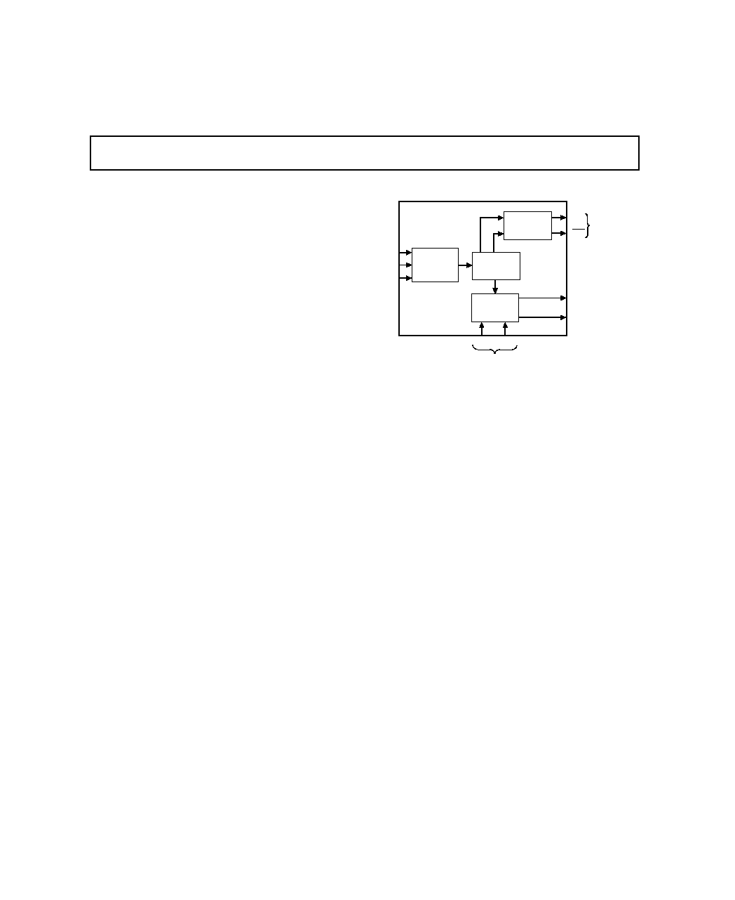
Programmable
Oscillator
FUNCTIONAL BLOCK DIAGRAM
FREQUENCY
SELECT
SINE WAVE
GENERATOR
PHASE
DETECT
LOGIC
SIN
COS
FROM
TRANSDUCER
FBIAS
SEL1
SEL2
AD2S99
EXC
SYNREF
SYNCHRONOUS
REFERENCE
LOS
TO
TRANSDUCER
PUSH/
PULL
O/P STAGE
EXC
PRODUCT HIGHLIGHTS
Dynamic Phase Compensation
The AD2S99 dynamically compensates for any phase variation
in a transducer by phase locking its synchronous reference out-
put to the transducer's secondary windings.
Programmable Excitation Frequency
The excitation frequency is easily programmed to 2 kHz, 5 kHz,
10 kHz, or 20 kHz by using the frequency select pins. Interme-
diate frequencies are available by adding an external resistor.
Signal Loss Detection
The AD2S99 has the ability to detect if both the transducer sec-
ondary winding connections become disconnected from its SIN
and COS inputs. The "LOS" output pin pulls high when a sig-
nal loss is detected.
Integration
The AD2S99 integrates the transducer excitation, synchronous
reference, and loss of signal detection functions into a small,
cost effective package.
GENERAL DESCRIPTION
The AD2S99 programmable sinusoidal oscillator provides sine
wave excitation for resolvers and a wide variety of ac transduc-
ers. The AD2S99 also provides a synchronous reference output
signal (3 V p-p square wave) that is phase locked to its SIN and
COS inputs. In an application, the SIN and COS inputs are
connected to the transducer's secondary windings.
The synchronous reference output compensates for temperature
and cabling dependent phase shifts and eliminates the need for
external preset phase compensation circuits. The synchronous
reference output can be used as a zero crossing reference for
resolver-to-digital converters such as Analog Devices' AD2S80A,
AD2S82A, AD2S83 and AD2S90.
The AD2S99 is packaged in a 20-pin PLCC and operates over
40
°
C to +85
°
C.
FEATURES
Programmable Sinusoidal Oscillator
Synthesized Synchronous Reference Output
Programmable Output Frequency Range: 2 kHz20 kHz
"Loss-of-Signal" Indicator
20-Pin PLCC Package
Low Cost
APPLICATIONS
Excitation Source for:
Resolvers
Synchros
LVDTs
RVDTs
Pressure Transducers
Load Cells
AC Bridges
© Analog Devices, Inc., 1995
One Technology Way, P.O. Box 9106, Norwood. MA 02062-9106, U.S.A.
Tel: 617/329-4700
Fax: 617/326-8703
AD2S99

AD2S99SPECIFICATIONS
Parameter
Min
Typ
Max
Units
Test Conditions
FREQUENCY OUTPUT RANGE
SEL1
SEL2
2 kHz
2000
Hz
V
SS
V
SS
5 kHz
5000
Hz
V
SS
GND
10 kHz
10000
Hz
GND
V
SS
20 kHz
20000
Hz
GND
GND
ACCURACY
Frequency
±
10
%
AP Grade @ +25
°
C
±
20
%
AP Grade 40
°
C to +85
°
C
±
5
%
BP Grade @ +25
°
C
±
10
%
BP Grade 40
°
C to +85
°
C
Amplitude
±
3
±
10
%
AP Grade @ +25
°
C
±
20
%
AP Grade 40
°
C to +85
°
C
±
3
±
5
%
BP Grade @ +25
°
C
±
10
%
BP Grade 40
°
C to +85
°
C
Power Supply Rejection Ratio
0.002
V p-p/V
Output Variation as Function of
Change in Power Supply Voltage
ANALOG OUTPUTS
Amplitude
EXC, EXC
2
V rms
EXC to GND, EXC to GND
SYNREF
±
3
V p-p
Square Wave
SYNREF OFFSET
±
200
mV
Current Drive Capability
EXC, EXC V
S
=
±
5 V
8
mA rms
R
LOAD
= 500
EXC to EXC
C
LOAD
= 1000 pF
Capacitive Drive
1000
pF
Total Harmonic Distortion
EXC, EXC
25
dB
ANALOG INPUTS SIN, COS
Amplitude
1.8
2.0
2.2
V rms
Phase Lock Range
45
+45
Degrees
Additional Phase Delay
±
10
Degrees
AP Grade
±
10
Degrees
BP Grade
FREQUENCY SELECT INPUTS
SEL1, SEL2
1
V
SS
AGND
V dc
LOS OUTPUT
Output Low Voltage
0.7
V dc
I
OL
= 400
µ
A
Output High Voltage
V
DD
V dc
50 k
Pull Up to V
DD
(Open
Drain Output)
SIN, COS LOS Threshold
0.5
0.6
0.8
V rms
POWER SUPPLIES
V
DD
+4.75
+5.25
V dc
V
SS
4.75
5.25
V dc
Quiescent Current I
DD
, I
SS
±
8
±
15
mA
No Load
TEMPERATURE RANGE
Operating
40
+85
°
C
Storage
65
+150
°
C
NOTES
1
Frequency select pins SEL1 and SEL2 must be connected to appropriate voltage levels before power is applied.
Specifications subject to change without notice.
REV. B
2
(V
S
= 4.75 V to 5.25 V @ 40 C to +85 C unless otherwise noted)
REV. B
3
AD2S99
ABSOLUTE MAXIMUM RATINGS*
V
DD
. . . . . . . . . . . . . . . . . . . . . . . . . . . . . . . . . . . . . . . . . +7 V
V
SS
. . . . . . . . . . . . . . . . . . . . . . . . . . . . . . . . . . . . . . . . . . 7 V
Operating Temperature . . . . . . . . . . . . . . . . . . 40
°
C to +85
°
C
Storage Temperature . . . . . . . . . . . . . . . . . . . 65
°
C to +150
°
C
Analog Input Voltages (SIN and COS) . . . . . . . . . V
SS
0.3 V
. . . . . . . . . . . . . . . . . . . . . . . . . . . . . . . . . . . . to V
DD
+ 0.3 V
Frequency Select (SEL1, SEL2) . . . . . . . . . . . . . . V
SS
0.4 V
. . . . . . . . . . . . . . . . . . . . . . . . . . . . . . . . . to AGND + 0.4 V
*Stresses above those listed under "Absolute Maximum Ratings" may cause
permanent damage to the device. This is a stress rating only and functional
operation of the device at these or any other conditions above those indicated in the
operational section of this specification is not implied. Exposure to absolute
maximum rating conditions for extended periods may affect device reliability.
RECOMMENDED OPERATING CONDITIONS
Power Supply Voltage (V
DD
to V
SS
) . . . . . .
±
4.75 V to
±
5.25 V
Analog Input Voltage (SIN and COS) . . . . . . . . 2 V rms
±
10%
Frequency Select (SEL1 and SEL2) . . . . . . . . . V
SS
to AGND
Operating Temperature Range . . . . . . . . . . . . . 40
°
C to +85
°
C
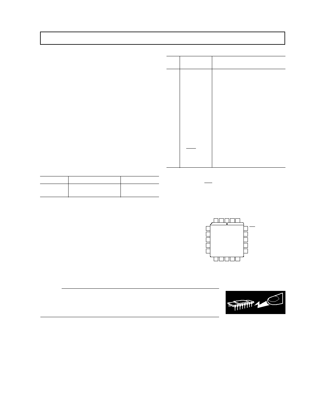
PIN DESIGNATIONS
Pin
No.
Mnemonic
Description
1
SEL2
Frequency Select 2
2
SEL1
Frequency Select 1
3
FBIAS
External Frequency Adjust Pin
5
SIN
Resolver Output SIN
6
1
DGND
Digital Ground
7
COS
Resolver Output COS
10
SYNREF
Synthesized Reference Output
11
LOS
Indicates When Both the SIN and
COS Are Below the Threshold.
12
V
DD
Positive Power Supply
16
1
AGND
Analog Ground
17
EXC
Resolver Reference One
18
EXC
Resolver Reference Two
3
19
2
V
SS
Negative Power Supply
20
2
V
SS
Negative Power Supply
NOTES
1
Pins 6 and 16 must be connected together.
2
Pins 19 and 20 must be connected together.
3
Resolver Reference two (EXC) is 180
°
phase advanced with respect to Resolver
Reference one (EXC).
PIN CONFIGURATION
NC = NO CONNECT
NC
SIN
NC
DGND
COS
FBIAS
SEL1
V
SS
SEL2
V
SS
NC
SYNREF
NC
LOS
V
DD
EXC
NC
AGND
NC
19
3
1
2
20
4
5
8
6
7
12 13
9
11
10
18
17
14
16
15
TOP VIEW
(Not to Scale)
AD2S99
EXC
ORDERING GUIDE
Model
Temperature Range
Package Option*
AD2S99AP
40
°
C to +85
°
C
P-20A
AD2S99BP
40
°
C to +85
°
C
P-20A
*P = PLCC.
WARNING!
ESD SENSITIVE DEVICE
CAUTION
ESD (electrostatic discharge) sensitive device. Electrostatic charges as high as 4000 V readily
accumulate on the human body and test equipment and can discharge without detection.
Although the AD2S99 features proprietary ESD protection circuitry, permanent damage may
occur on devices subjected to high energy electrostatic discharges. Therefore, proper ESD
precautions are recommended to avoid performance degradation or loss of functionality.
AD2S99
REV. B
4
20
0
6
2
4
4
0
12
8
10
14
16
18
28
24
20
16
12
8
ADDITIONAL RESISTANCE k
RESISTOR PULLUP TO V
DD
FROM FBIAS
FREQUENCY kHz
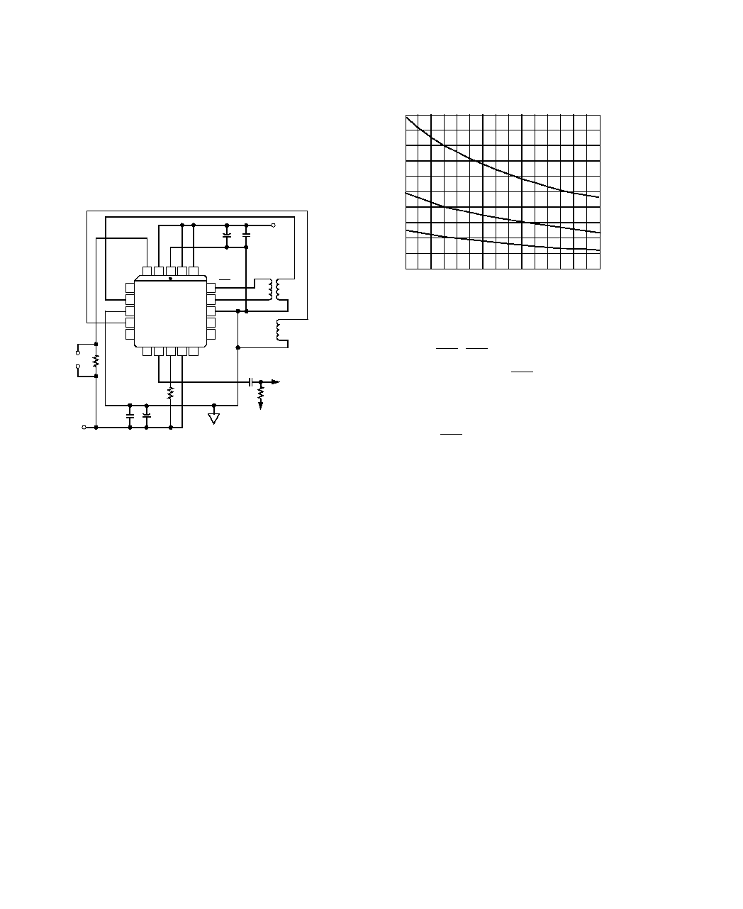
Figure 2. Typical Added Resistance Value
AD2S99 OSCILLATOR OUTPUT STAGE
The output of the AD2S99 oscillator consists of two sinusoidal
signals, EXC, and EXC. EXC is 180
°
phase advanced with re-
spect to EXC. The excitation winding of a transducer should be
connected across EXC (Pin 17) and EXC (Pin 18).
With low impedance transducers, it may be necessary to in-
crease the output current drive of the AD2S99. In such an in-
stance, an external buffer amplifier can be used to provide gain
(as needed), and additional current drive for the excitation out-
put (either EXC or EXC) of the AD2S99, providing a single
ended drive to the transducer. Refer to Figures 6, 7 and 8 for
sample buffer configurations.
The amplitude modulated SIN and COS output signals from a re-
solver should be connected as feedback signals to the AD2S99.
The SYNREF output compensates for any primary to secondary
phase errors in the resolver. These errors can degrade the accuracy
of a Resolver-to-Digital Converter (R/D Converter).
SIN, from the resolver, should be connected to the AD2S99 SIN
input and COS should be connected to the AD2S99 COS input.
The SIN Lo, COS Lo (resolver signal returns) should be con-
nected to AGND and the R/D Converter as applicable.
The synthesized reference (SYNREF) from the AD2S99 should
be connected to the reference input pin of the R/D Converter.
The SYNREF signal is a square wave at the oscillator frequency
of amplitude
±
3 V p-p and is phase coherent with the SIN and
COS inputs. If this signal is used to drive the reference input of
the AD2S90 R/D Converter, a coupling capacitor and resistor to
GND must be connected between the SYNREF output of the
AD2S99 and the REF input of the R/D Converter (see Figure
3). Please read the appropriate R/D Converter data sheets for
further clarification.
LOSS OF SIGNAL
During normal operation when both the SIN and COS signals
on the resolver secondary windings are connected to the
AD2S99, the LOS output pin of the AD2S99 (Pin 11) is at a
Logic Lo (
<
0.7 V). If both the SIN and COS signals on the re-
solver secondary windings fall below the LOS threshold level of
the AD2S99, the LOS pin of the AD2S99 will pull up to a
Logic Hi (V
DD
) level.
CONNECTING THE AD2S99 OSCILLATOR
Refer to Figure 1. Positive supply voltage V
DD
should be con-
nected to Pin 12 and negative supply voltage V
SS
should be con-
nected to both Pins 19 and 20. Reversal of these power supplies will
destroy the device. The appropriate voltage level for the power
supplies is
±
5 V dc
±
5%. Both V
SS
Pins (19 and 20) must be
connected together, and Digital Ground (Pin 6) must be con-
nected to Analog Ground (Pin 16) locally at the AD2S99.
V
DD
NC = NO CONNECT
NC
SIN
NC
DGND
COS
FBIAS
SEL1
V
SS
SEL2
V
SS
NC
SYNREF
NC
LOS
V
DD
EXC
NC
AGND
NC
19
3
1
2
20
4
5
8
6
7
12
13
9
11
10
18
17
14
16
15
AD2S99
EXC
0.1
µ
F
V
SS
4.7
µ
F
REF
RESOLVER
SIN
0.1
µ
F
4.7
µ
F
R
X
*
TO AD2S80/
AD2S90 REF INPUT
50k
*
R
X
IS ONLY REQUIRED FOR INTERMEDIATE FREQUENCIES.
FIXED FREQUENCIES ONLY REQUIRE A LINK.
SEL2 = GND ]
SEL1 = V
SS
]
5kHz MODE
INCREASE R
X
TO LOWER
OUTPUT FREQUENCY
(SEE GRAPH)
COS
.
.
.
100nF
100k
Figure 1. Typical Configuration
It is recommended that decoupling capacitors are connected in
parallel between V
DD
and Analog Ground and V
SS
and Analog
Ground in close proximity to the AD2S99. The recommended
values for the decoupling capacitors are 100 nF (ceramic) and
4.7
µ
F (tantalum). When multiple AD2S99s are used, separate
decoupling capacitors should be used for each AD2S99.
FREQUENCY ADJUSTMENT
The output frequency of the AD2S99 is programmable to four
standard frequencies (2, 5, 10, or 20 kHz) using the SEL1 and
SEL2 pins. The output can also be adjusted to provide interme-
diate frequencies by connecting a resistor from the FBIAS pin to
the positive supply V
DD
. The FBIAS pin is connected directly to
V
DD
during normal operation. A graph showing the typical
added resistance values for various intermediate frequencies is
provided in Figure 2. The procedure for obtaining an intermedi-
ate frequency is:
1. Set the output frequency via the SEL1, SEL2 pins to the fre-
quency immediately above the required intermediate frequency.
2. Connect the frequency adjust pin FBIAS to V
DD
via an exter-
nal resistor.
For example: to obtain an output frequency of 8 kHz, set the
nominal output frequency to 10 kHz by connecting SEL1 to
GND and SEL2 to V
SS
. Connect FBIAS to V
DD
via a 6 k
resistor (refer to Figure 2).
REV. B
5
AD2S99
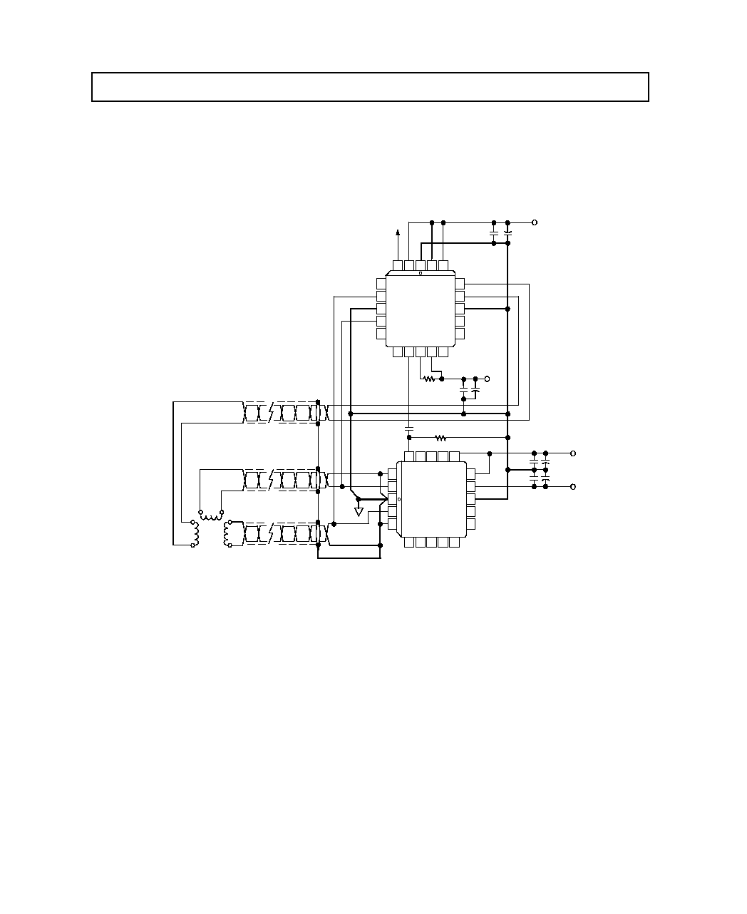
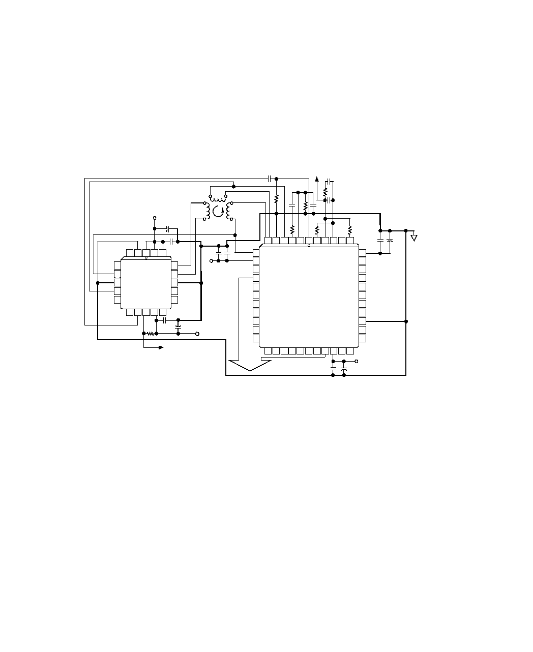
AD2S99/AD2S90 TYPICAL CONFIGURATION
Figure 3 shows a typical circuit configuration for the AD2S99
Oscillator and the AD2S90 Resolver-to-Digital Converter. The
maximum level of the SIN and COS input signals to the
AD2S90 should be 2 V rms
±
10%. All the analog ground sig-
nals should be star connected to the AD2S90 AGND pin. If
shielded twisted pair cables are used for the resolver signals, the
shields should also be terminated at the AD2S90 AGND pin.
The SYNREF output of the AD2S99 should be connected to
the REF input pin of the AD2S90 via a 0.1
µ
F capacitor with a
100 k
resistor to GND. This is to block out any dc offset in
the SYNREF signal. For more detailed information please refer
to the AD2S90 data sheet.
NC = NO CONNECT
NC
SIN
NC
DGND
COS
EXC
EXC
NC
AGND
NC
19
3
1
2
20
4
5
8
6
7
12 13
9
11
10
18
17
14
16
15
TOP VIEW
(Not to Scale)
AD2S99
SEL1
V
SS
SEL2
V
SS
NC
SYNREF
NC
LOS
V
DD
19
3
1
2
20
4
5
8
6
7
12
13
9
11
10
18 17
14
16 15
4.7µF
4.7µF
0.1µF
0.1µF
COS
SIN
REF
S2
S4
S3
S1
R4
R2
RESOLVER
REF
COS
AGND
SIN
SIN LO
V
DD
V
SS
DGND
AD2S90
TOP VIEW
(Not to Scale)
0.1µF
100k
V
DD
V
SS
V
DD
0.1µF
50k
4.7µF
0.1µF
4.7µF
V
SS
SEL2 = GND
SEL1 = V
SS
F
OUT
= 5kHz
COS LO
S4
S3
S1
S2
V
DD
POWER
RETURN
FBIAS
V
DD
Figure 3. AD2S99 and AD2S90 Example Configuration
AD2S99
REV. B
6
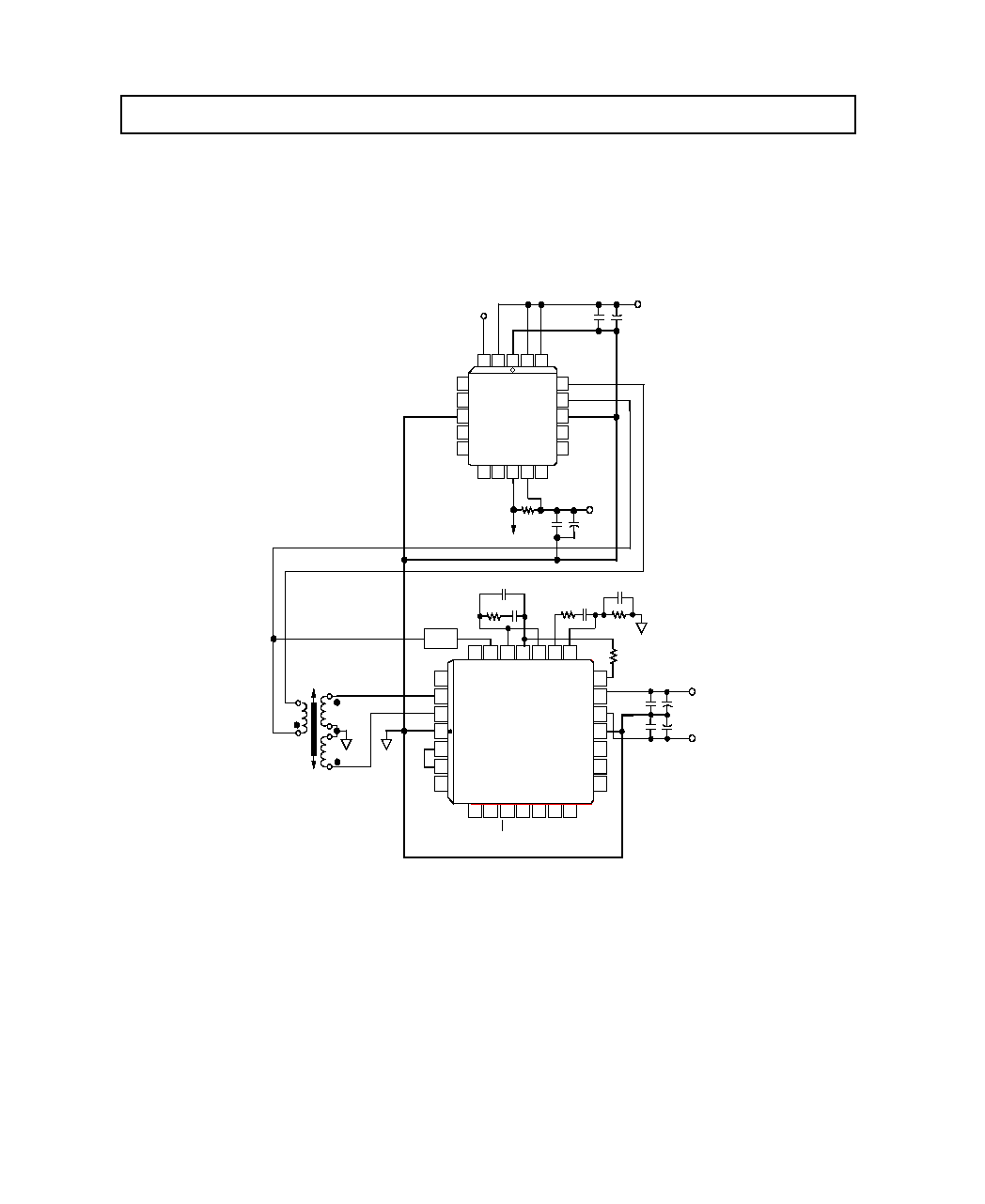
AD2S99/AD2S82A TYPICAL CONFIGURATION
Figure 4 shows a typical circuit configuration for the AD2S99
Oscillator and the AD2S82A Resolver-to-Digital Converter.
The maximum level of the SIN and COS input signals to the
AD2S82A should be 2 V rms
±
10%. All the analog ground sig-
nals should be star connected to the AD2S82A AGND pin. If
shielded twisted pair cables are used for the resolver signals, the
shields should also be terminated at the AD2S82A AGND pin.
Coupling capacitor C3, and resistor to GND R3, between the
SYNREF output of the AD2S99 and the REF input pin of the
AD2S82A are optional. For additional information on selecting
component values for the AD2S82A, please refer to the
AD2S82A data sheet or the application note "Passive Compo-
nent Selection and Dynamic Modeling for the AD2S80 Series
Resolver-to-Digital Converters" (AN-266).
44
1
2
6
4
5
21
24
23
22
18
20
19
39
38
35
34
33
37
36
3
7
8
11
12
13
9
10
40
41
42
25
28
27
26
43
31
30
29
32
15
16
17
14
TOP VIEW
(Not to Scale)
AD2S82A
DB2
DB6
SIN
I/P
+V
S
MSB DB1
NC
DB3
DB4
DB5
DB7
DB8
V
S
RC
DATA LOAD
COMP
SC2
DIR
BUSY
INHIBIT
NC
SC1
DIGITAL GND
SIG GND
A GND
DEMOD I/P
INTEGRATOR O/P
DEMOD O/P
COS I/P
AC ERROR O/P
REFERENCE I/P
VCO O/P
VCO I/P
INTEGRATOR I/P
DB9
DB10
DB13
DB14
DB15
DB11
DB12
ENABLE
BYTE
SELECT
LSB DB16
+V
L
COS
SIN
REF
RESOLVER
AGND
0V
12V
R6
R4
R1
C5
R5
C4
C2
C1
R2
C3
R3
R3, C3 OPTIONAL
VELOCITY
OUTPUT
+12V
AGND
+5V
DGND
DIGITAL
OUTPUT
DATA
+5V
10µF
0.1µF
0.1µF
10µF
0.1µF
10µF
NC = NO CONNECT
NC
SIN
NC
DGND
COS
EXC
EXC
NC
AGND
NC
19
3
1
2
20
4
5
8
6
7
12 13
9
11
10
18
FBIAS
17
14
16
15
TOP VIEW
(Not to Scale)
AD2S99
NC
SYNREF
NC
V
DD
LOS
SEL1
V
SS
SEL2
V
SS
5V
SYNREF
COS
SIN
50k
LOS
SEL1 = GND
SEL2 = V
SS
F
OUT
= 10kHz
0.1µF
4.7µF
0.1µF
4.7µF
FBIAS
Figure 4. AD2S99 and AD2S82A Example Configuration
REV. B
7
AD2S99
AD2S99/AD2S93 TYPICAL CONFIGURATION
Figure 5 shows a typical circuit configuration for the AD2S99
Oscillator and the AD2S93 LVDT-to-Digital Converter. The
maximum level of the A and B transducer input signals to the
AD2S93 should be 1 V rms
±
20%. All the analog ground sig-
nals should be star connected to the AD2S93 AGND pin. If
shielded twisted pair cables are used for the LVDT signals, the
shields should also be terminated at the AD2S93 AGND pin.
The SYNREF output of the AD2S99 cannot be used as the
REF input signal for the AD2S93. The zero crossing reference
for the AD2S93 should be taken from the primary winding of
the LVDT through a phase lead or lag network. The phase com-
pensation network ensures that the REF input is phase coherent
with the A and B input signals to the AD2S93.
NC = NO CONNECT
NC
SIN
NC
DGND
COS
EXC
EXC
NC
AGND
NC
19
3
1
2
20
4
5
8
6
7
12 13
9
11
10
18
17
14
16
15
TOP VIEW
(Not to Scale)
AD2S99
FBIAS
SEL1
V
SS
SEL2
V
SS
NC
SYNREF
NC
LOS
V
DD
4.7µF
4.7µF
0.1µF
0.1µF
SEC
PRI
LVDT
V
DD
V
SS
V
DD
0.1µF
50k
4.7µF
0.1µF
4.7µF
V
SS
SEL2 = GND
SEL1 = V
SS
F
OUT
= 5kHz
V
DD
NC = NO CONNECT
DATA
SCLK
UNR
CLKOUT
NC
NC
26
27
28
4
2
3
15
18
17
16
12
14
13
25 24
21 20 19
23 22
1
5
6
9
10
11
7
8
CS
R2
C2
C1
C3
R5
R6
R7
C4
DMODOUT
B
A
PHASE
COMP
LOS
TOP VIEW
(Not to Scale)
AD2S93
B
NC
LOS
GAIN
DIFF
AGND
A
V
SS
DGND
DIR
NULL
OVR
REF
NC
VEL
DMODIN
ACERROR
VGAIN
INTIN
V
DD
Figure 5. AD2S99 and AD2S93 Example Configuration
AD2S99
REV. B
8
+V
S
SSM2142
4
6
7
8
5
2
1
3
V
S
NC = NO CONNECT
NC
SIN
NC
DGND
COS
EXC
EXC
NC
AGND
NC
19
3
1
2
20
4
5
8
6
7
12 13
9
11
10
18
17
14
16
15
TOP VIEW
(Not to Scale)
AD2S99
FBIAS
SEL1
V
SS
SEL2
V
SS
NC
SYNREF
NC
LOS
V
DD
*
*
*
OPTIONAL; CONSULT APPROPRIATE
ANALOG DEVICES DATA SHEET.
RESOLVER
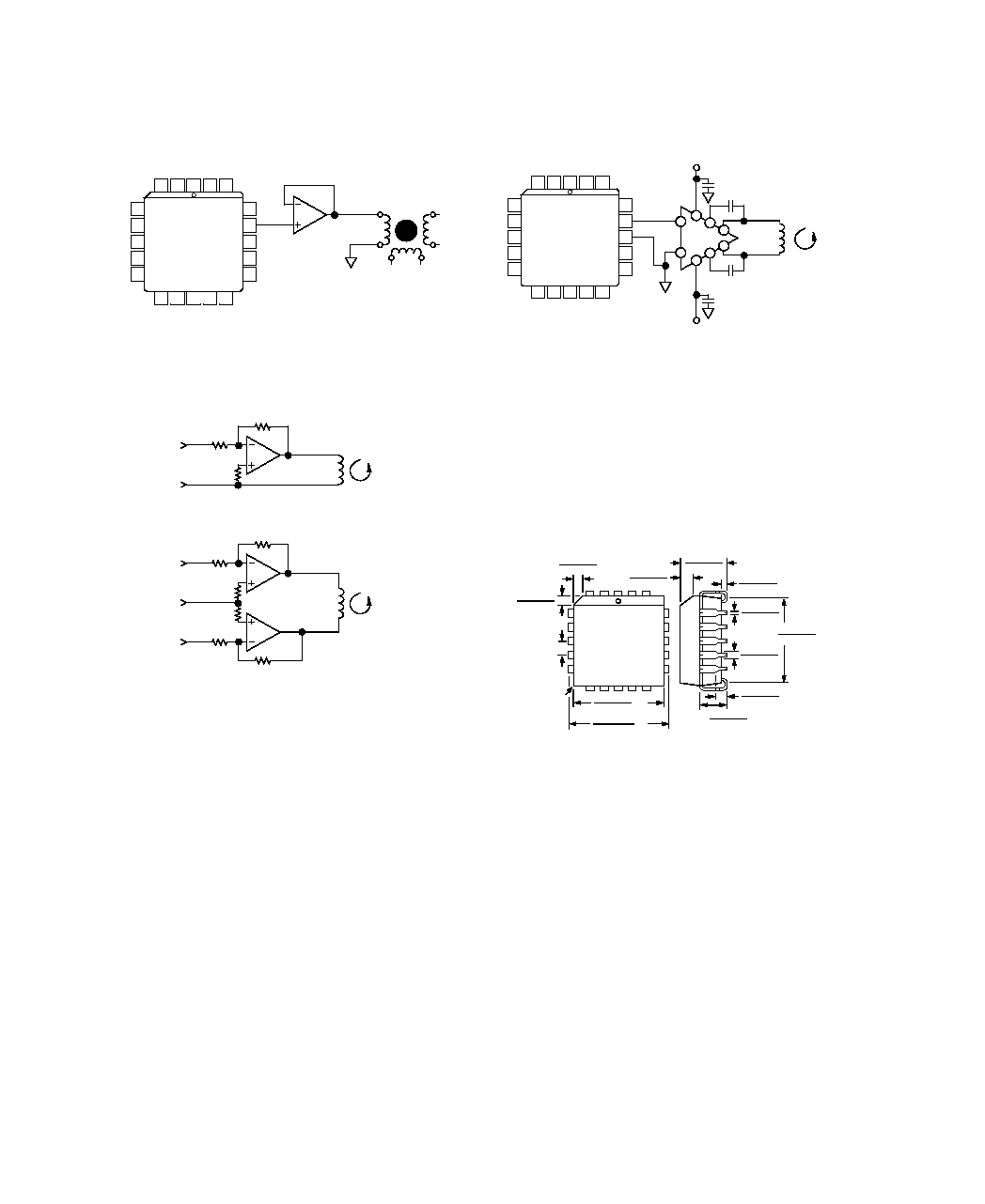
Figure 8. The SSM2142 as a Single Ended to Differential
Driver
OUTLINE DIMENSIONS
Dimensions shown in inches and (mm).
PLCC (P-20A)
0.395 (10.02)
0.385 (9.78)
SQ
0.110 (2.79)
0.085 (2.16)
0.330 (8.38)
0.290 (7.37)
0.048 (1.21)
0.042 (1.07)
0.356 (9.04)
0.350 (8.89)
SQ
0.048 (1.21)
0.042 (1.07)
0.050
(1.27)
BSC
0.020
(0.50)
R
19
3
TOP VIEW
18
14
9
8
PIN 1
IDENTIFIER
4
13
0.032 (0.81)
0.026 (0.66)
0.021 (0.53)
0.013 (0.33)
0.056 (1.42)
0.042 (1.07)
0.025 (0.63)
0.015 (0.38)
0.040 (1.01)
0.025 (0.64)
0.180 (4.57)
0.165 (4.19)
COS
SIN
REF
V
OUT
V
OUT
= 2V
RMS
NC = NO CONNECT
NC
SIN
NC
DGND
COS
EXC
EXC
NC
AGND
NC
19
3
1
2
20
4
5
8
6
7
12 13
9
11
10
18
17
14
16
15
TOP VIEW
(Not to Scale)
AD2S99
FBIAS
SEL1
V
SS
SEL2
V
SS
NC
SYNREF
NC
LOS
V
DD
Figure 6. Sample Buffer Configuration
V
OUT
V
OUT
= 2V
RMS
x
(
)
RESOLVER
V
IN
EXC
PIN 16
PIN 17
AGND
R1
R2
R1
R2
V
OUT
V
OUT
= 2V
RMS
x 2 x
(
)
RESOLVER
V
IN
EXC
PIN 16
PIN 17
AGND
R1
R2
R1
R2
R1
R2
EXC
PIN 18
OP279
OP279
A SUITABLE AMPLIFIER FOR ABOVE IS THE OP279
Figure 7. Sample Buffer Configurations
C1978b106/95
PRINTED IN U.S.A.