 | ÐлекÑÑоннÑй компоненÑ: AD2S90 | СкаÑаÑÑ:  PDF PDF  ZIP ZIP |
Äîêóìåíòàöèÿ è îïèñàíèÿ www.docs.chipfind.ru
FUNCTIONAL BLOCK DIAGRAM
HIGH ACCURACY
SIN COS
MULTIPLIER
UP-DOWN
COUNTER
LATCH
SERIAL INTERFACE
HIGH
DYNAMIC
RANGE V.C.O.
P.S.D. AND
FREQUENCY
SHAPING
DECODE
LOGIC
SIN
SIN LO
COS
NMC
A
B
NM
SCLK
DATA
REF
VEL
CLKOUT
DIR
ERROR
AMPLIFIER
CLK
U/D
ANGLE
CS
SIN (
)
COS LO
DIGITAL
ANGLE
REV. D
Information furnished by Analog Devices is believed to be accurate and
reliable. However, no responsibility is assumed by Analog Devices for its
use, nor for any infringements of patents or other rights of third parties
which may result from its use. No license is granted by implication or
otherwise under any patent or patent rights of Analog Devices.
a
FEATURES
Complete Monolithic Resolver-to-Digital Converter
Incremental Encoder Emulation (1024-Line)
Absolute Serial Data (12-Bit)
Differential Inputs
12-Bit Resolution
Industrial Temperature Range
20-Lead PLCC
Low Power (50 mW)
APPLICATIONS
Industrial Motor Control
Servo Motor Control
Industrial Gauging
Encoder Emulation
Automotive Motion Sensing and Control
Factory Automation
Limit Switching
AD2S90
GENERAL DESCRIPTION
The AD2S90 is a complete 12-bit resolution tracking resolver-
to-digital converter. No external components are required to
operate the device.
The converter accepts 2 V rms
±
10% input signals in the range
3 kHz20 kHz on the SIN, COS and REF inputs. A Type II
servo loop is employed to track the inputs and convert the input
SIN and COS information into a digital representation of the
input angle. The bandwidth of the converter is set internally at
1 kHz within the tolerances of the device. The guaranteed maxi-
mum tracking rate is 500 rps.
Angular position output information is available in two forms,
absolute serial binary and incremental A quad B.
The absolute serial binary output is 12-bit (1 in 4096). The data
output pin is high impedance when Chip Select
CS is logic HI.
This allows the connection of multiple converters onto a com-
mon bus. Absolute angular information in serial pure binary
form is accessed by
CS followed by the application of an exter-
nal clock (SCLK) with a maximum rate of 2 MHz.
The encoder emulation outputs A, B and NM continuously
produce signals equivalent to a 1024 line encoder. When de-
coded this corresponds to 12 bits of resolution. Three common
north marker pulsewidths are selected via a single pin (NMC).
An analog velocity output signal provides a representation of
velocity from a rotating resolver shaft traveling in either a clock-
wise or counterclockwise direction.
The AD2S90 operates on
±
5 V dc
±
5% power supplies and is
fabricated on Analog Devices' Linear Compatible CMOS pro-
cess (LC
2
MOS). LC
2
MOS is a mixed technology process that
combines precision bipolar circuits with low power CMOS logic
circuits.
PRODUCT HIGHLIGHTS
Complete Resolver-Digital Interface. The AD2S90 provides
the complete solution for digitizing resolver signals (12-bit reso-
lution) without the need for external components.
Dual Format Position Data. Incremental encoder emulation
in standard A QUAD B format with selectable North Marker
width. Absolute serial 12-bit angular binary position data
accessed via simple 3-wire interface.
Single High Accuracy Grade in Low Cost Package.
±
10.6 arc
minutes of angular accuracy available in a 20-lead PLCC.
Low Power. Typically 50 mW power consumption.
Low Cost, Complete 12-Bit
Resolver-to-Digital Converter
One Technology Way, P.O. Box 9106, Norwood, MA 02062-9106, U.S.A.
Tel: 781/329-4700
World Wide Web Site: http://www.analog.com
Fax: 781/326-8703
© Analog Devices, Inc., 1999

Parameter
Min
Typ
Max
Units
Test Condition
SIGNAL INPUTS
Voltage Amplitude
1.8
2.0
2.2
V rms
Sinusoidal Waveforms, Differential
SIN to SINLO, COS to COSLO
Frequency
3
20
kHz
Input Bias Current
100
nA
V
IN
= 2
±
10% V rms
Input Impedance
1.0
M
V
IN
= 2
±
10% V rms
Common-Mode Volts
1
100
mV peak
CMV @ SINLO, COSLO w.r.t.
CMRR
60
dB
AGND @ 10 kHz
REFERENCE INPUT
Voltage Amplitude
1.8
2.0
3.35
V rms
Sinusoidal Waveform
Frequency
3
20
kHz
Input Bias Current
100
nA
Input Impedance
100
k
Permissible Phase Shift
10
+10
Degrees
Relative to SIN, COS Inputs
CONVERTER DYNAMICS
Bandwidth
700
840
1000
Hz
Maximum Tracking Rate
500
rps
Maximum VCO Rate (CLKOUT)
2.048
MHz
Settling Time
1
°
Step
2
7
ms
179
°
Step
20
ms
ACCURACY
Angular Accuracy
2
±
10.6 + 1 LSB
arc min
Repeatability
3
1
LSB
VELOCITY OUTPUT
Scaling
120
150
180
rps/V dc
Output Voltage at 500 rps
±
2.78
±
3.33
±
4.17
V dc
Load Drive Capability
±
250
µ
A
V
OUT
=
±
2.5 V dc (typ), R
L
10 k
LOGIC INPUTS SCLK,
CS
Input High Voltage (V
INH
)
3.5
V dc
V
DD
= +5 V dc, V
SS
= 5 V dc
Input Low Voltage (V
INL
)
1.5
V dc
V
DD
= +5 V dc, V
SS
= 5 V dc
Input Current (I
IN
)
10
µ
A
Input Capacitance
10
pF
LOGIC OUTPUTS DATA, A, B,
4
NM, CLKOUT, DIR
V
DD
= +5 V dc, V
SS
= 5 V dc
Output High Voltage
4.0
V dc
I
OH
= 1 mA
Output Low Voltage
1.0
V dc
I
OL
= 1 mA
0.4
V dc
I
OL
= 400
µ
A
SERIAL CLOCK (SCLK)
SCLK Input Rate
2
MHz
NORTH MARKER CONTROL (NMC)
90
°
+4.75
+5.0
+5.25
V dc
North Marker Width Relative to
180
°
0.75
DGND
+0.75
V dc
"A" Cycle
360
°
4.75
5.0
5.25
V dc
POWER SUPPLIES
V
DD
+4.75
+5.00
+5.25
V dc
V
SS
4.75
5.00
5.25
V dc
I
DD
10
mA
I
SS
10
mA
NOTES
1
If the tolerance on signal inputs =
±
5%, then CMV = 200 mV.
2
1 LSB = 5.3 arc minute.
3
Specified at constant temperature.
4
Output load drive capability.
Specifications subject to change without notice.
AD2S90SPECIFICATIONS
(V
DD
= +5 V 5%, V
SS
= 5 V 5%, AGND = DGND = 0 V, T
A
= 40 C to +85 C unless
otherwise noted)
REV. D
2
AD2S90
REV. D
3
AD2S90
Parameter
Min
Max
Units
Test Conditions/Notes
t
DIR
200
ns
DIR to CLKOUT Positive Edge
t
CLK
250
400
ns
CLKOUT Pulsewidth
t
ABN
250
ns
CLKOUT Negative Edge to A, B and NM Transition
Parameter
AD2S90
Units
Test Conditions/Notes
t
1
150
ns max
CS to DATA Enable
t
2
1
600
ns min
CS to 1st SCLK Negative Edge
t
3
250
ns min
SCLK Low Pulse
t
4
250
ns min
SCLK High Pulse
t
5
100
ns max
SCLK Negative Edge to DATA Valid
t
6
600
ns min
CS High Pulsewidth
t
7
150
ns max
CS High to DATA High Z (Bus Relinquish)
NOTE
1
SCLK can only be applied after t
2
has elapsed.
(V
DD
= +5 V 5%, V
SS
= 5 V 5%, AGND = DGND = 0 V, T
A
= 40 C to +85 C unless
otherwise noted)
TIMING CHARACTERISTICS
1, 2
LSB
MSB
t
3
t
4
t
5
t
1
t
7
t
6
t*
t
2
*
THE MINIMUM ACCESS TIME: USER DEPENDENT
CSB
SCLK
DATA
Figure 1. Serial Interface
NOTES
1
Timing data are not 100% production tested. Sample tested at +25
°
C only to ensure conformance to data sheet limits. Logic output timing tests carried out using
10 pF, 100 k
load.
2
Capacitance of data pin in high impedance state = 15 pF.
A
B
90
180
NM
NUMBER OF DEGREES REFERS TO WIDTH RELATIVE TO "A" CYCLE
360
Figure 2. Incremental Encoder
CLKOUT
A, B, NM
DIR
COUNTER IS CLOCKED
ON THIS EDGE
t
DIR
t
ABN
t
CLK
Figure 3. DIR/CLKOUT/A, B and NM Timing
AD2S90
REV. D
4
RECOMMENDED OPERATING CONDITIONS
Power Supply Voltage (V
DD
V
SS
) . . . . . . . . . .
±
5 V dc
±
5%
Analog Input Voltage (SIN, COS & REF) . . . . . 2 V rms
±
10%
Signal and Reference Harmonic Distortion . . . . . . . . . . . . 10%
Phase Shift between Signal and Reference . . . . . . . . . . . . .
±
10
°
Ambient Operating Temperature Range
Industrial (AP) . . . . . . . . . . . . . . . . . . . . . . . 40
°
C to +85
°
C
ABSOLUTE MAXIMUM RATINGS*
V
DD
to AGND . . . . . . . . . . . . . . . . . . . . 0.3 V dc to +7.0 V dc
V
SS
to AGND . . . . . . . . . . . . . . . . . . . . +0.3 V dc to 7.0 V dc
AGND to DGND . . . . . . . . . . . . 0.3 V dc to V
DD
+ 0.3 V dc
Analog Inputs to AGND
REF . . . . . . . . . . . . . . . . . . V
SS
0.3 V dc to V
DD
+ 0.3 V dc
SIN, SIN LO . . . . . . . . . . . V
SS
0.3 V dc to V
DD
+ 0.3 V dc
COS, COS LO . . . . . . . . . . V
SS
0.3 V dc to V
DD
+ 0.3 V dc
Analog Output to AGND
VEL . . . . . . . . . . . . . . . . . . . . . . . . . . . . . . . . . . . V
SS
to V
DD
Digital Inputs to DGND, CSB,
SCLK, RES . . . . . . . . . . . . . . . 0.3 V dc to V
DD
+ 0.3 V dc
Digital Outputs to DGND, NM, A, B,
DIR, CLKOUT DATA . . . . . . 0.3 V dc to V
DD
+ 0.3 V dc
Operating Temperature Range
Industrial (AP) . . . . . . . . . . . . . . . . . . . . . . . 40
°
C to +85
°
C
Storage Temperature Range . . . . . . . . . . . . . 65
°
C to +150
°
C
Lead Temperature (Soldering 10 sec) . . . . . . . . . . . . . . 300
°
C
Power Dissipation to +75
°
C . . . . . . . . . . . . . . . . . . . . 300 mW
Derates above +75
°
C by . . . . . . . . . . . . . . . . . . . . . 10 mW/
°
C
*Stresses above those listed under Absolute Maximum Ratings may cause perma-
nent damage to the device. This is a stress rating only; functional operation of the
device at these or any other conditions above those indicated in the operational
section of this specification is not implied. Exposure to absolute maximum rating
conditions for extended periods may affect device reliability.
ORDERING GUIDE
Model
Temperature Range Accuracy
Package Option
AD2S90AP 40
°
C to +85
°
C
10.6 arc min P-20A
CAUTION
The AD2S90 features an input protection circuit consisting of large "distributed" diodes and
polysilicon series resistors to dissipate both high energy discharges (Human Body Model) and
fast, low energy pulses (Charges Device Model).
Proper ESD precautions are strongly recommended to avoid functional damage or performance
degradation. For further information on ESD precautions, refer to Analog Devices ESD
Prevention Manual.
PIN DESCRIPTIONS
Pin
No. Mnemonic Function
1
AGND
Analog ground, reference ground.
2
SIN
SIN channel noninverting input connect to
resolver SIN HI output. SIN to SIN LO =
2 V rms
±
10%.
3
SIN LO
SIN channel inverting input connect to
resolver SIN LO.
4
DATA
Serial interface data output. High impedance
with
CS = HI. Enabled by CS = 0.
5
SCLK
Serial interface clock. Data is clocked out on
"first" negative edge of SCLK after a LO transi-
tion on
CS. 12 SCLK pulses to clock data out.
6
CS
Chip select. Active LO. Logic LO transition
enables DATA output.
7
A
Encoder A output.
8
B
Encoder B output.
9
NM
Encoder North Marker emulation output.
Pulse triggered as code passes through zero.
Three common pulsewidths available.
10
DIR
Indicates direction of rotation of input.
Logic HI = increasing angular rotation.
Logic LO = decreasing angular rotation.
11
DGND
Digital power ground return.
12
V
SS
Negative power supply, 5 V dc
±
5%.
13
V
DD
Positive power supply, +5 V dc
±
5%.
14
V
DD
Positive power supply, +5 V dc
±
5%. Must
be connected to Pin 13.
15
NMC
North marker width control. Internally pulled
HI via 50 k
nominal.
16
CLKOUT
Internal VCO clock output. Indicates angular
velocity of input signals. Max nominal rate =
1.536 MHz. CLKOUT is a 300 ns positive pulse.
17
VEL
Indicates angular velocity of input signals.
Positive voltage w.r.t. AGND indicates in-
creasing angle. FSD = 375 rps.
18
REF
Converter reference input. Normally derived
from resolver primary excitation. REF = 2 V
rms nominal. Phase shift w.r.t. COS and SIN
=
±
10
°
max
19
COS LO
COS channel inverting input. Connect to
resolver COS LO.
20
COS
COS channel noninverting input. Connect to
resolver COS HI output. COS = 2 V rms
±
10%.
3 2 1 20 19
9 10 11 12 13
18
17
16
15
14
4
5
6
7
8
TOP VIEW
(Not to Scale)
PIN 1
IDENTIFIER
DATA
SCLK
CS
A
B
REF
VEL
CLKOUT
NMC
V
DD
AD2S90
SIN LO
SIN
AGND
COS
COS LO
NM
DIR
DGND
V
SS
V
DD
WARNING!
ESD SENSITIVE DEVICE
PIN CONFIGURATION
AD2S90
REV. D
5
For more information on the operation of the converter, see
Circuit Dynamics section.
S2 TO S4
(COS)
0
S3 TO S1
(SIN)
R2 TO R4
(REF)
90
180
270
360
Figure 4. Electrical and Physical Resolver Representation
Connecting The Converter
Refer to Figure 4. Positive power supply V
DD
= +5 V dc
±
5%
should be connected to Pin 13 & Pin 14 and negative power
supply V
SS
= 5 V dc
±
5% to Pin 12. Reversal of these power
supplies will destroy the device. S3 (SIN) and S2 (COS)
from the resolver should be connected to the SIN and COS pins
of the converter. S1 (SIN) and S4 (COS) from the resolver
should be connected to the SINLO and COSLO pins of the
converter. The maximum signal level of either the SIN or COS
resolver outputs should be 2 V rms
±
10%. The AD2S90
AGND pin is the point at which all analog signal grounds should
be star connected. The SIN LO and COS LO pins on the
AD2S90 should be connected to AGND. Separate screened
twisted cable pairs are recommended for all analog inputs SIN,
COS, and REF. The screens should terminate at the converter
AGND pin.
North marker width selection is controlled by Pin 15, NMC.
Application of V
DD
, 0 V, or V
SS
to NMC will select standard
90
°
, 180
°
and 360
°
pulsewidths. If unconnected, the NM pulse
defaults to 90
°
. For a more detailed description of the output
formats available see the Position Output section.
RESOLVER FORMAT SIGNALS
A resolver is a rotating transformer which has two stator wind-
ings and one rotor winding. The stator windings are displaced
mechanically by 90
°
(see Figure 4). The rotor is excited with an
ac reference. The amplitude of subsequent coupling onto the
stator windings is a function of the position of the rotor (shaft)
relative to the stator. The resolver, therefore, produces two
output voltages (S3S1, S2S4) modulated by the SINE and
COSINE of shaft angle. Resolver format signals refer to the
signals derived from the output of a resolver. Equation 1 illus-
trates the output form.
S3S1 = E
O
SIN
t · SIN
S2S4 = E
O
SIN
t · COS
(1)
where:
= shaft angle
SIN
t = rotor excitation frequency
E
O
= rotor excitation amplitude
Principle of Operation
The AD2S90 operates on a Type 2 tracking closed-loop prin-
ciple. The output continually tracks the position of the resolver
without the need for external convert and wait states. As the
transducer moves through a position equivalent to the least
significant bit weighting, the output is updated by one LSB.
On the AD2S90, CLKOUT updates corresponding to one LSB
increment. If we assume that the current word state of the
up-down counter is
, S3S1 is multiplied by COS
and S2S4
is multiplied by SIN
to give:
E
O
SIN
t · SIN
COS
E
O
SIN
t · COS
SIN
(2)
An error amplifier subtracts these signals giving:
E
O
SIN
· (SIN
COS
COS
SIN
)
or
E
O
SIN
t · SIN (
)
(3)
where (
) = angular error
A phase sensitive detector, integrator and voltage controlled
oscillator (VCO) form a closed loop system which seeks to null
sin (
). When this is accomplished the word state of the
up/down counter,
, equals within the rated accuracy of the
converter, the resolver shaft angle
.
OSCILLATOR
TWISTED PAIR
SCREENED
CABLE
S3
S1
S1
S3
S2
S4
POWER RETURN
RESOLVER
10nF
47 F
10nF
47 F
+5V
5V
0V (POWER GROUND)
15
16
17
18
14
19
20
1
2
3
AD2S90AP
REF
COS LO
COS
AGND
SIN
SIN LO
DGND
7
6
5
4
8
13
12
11
10
9
V
DD
R2
R1
S4
S2
V
DD
V
SS
Figure 5. Connecting the AD2S90 to a Resolver
AD2S90
REV. D
6
ABSOLUTE POSITION OUTPUT
SERIAL INTERFACE
Absolute angular position is represented by serial binary data
and is extracted via a three-wire interface, DATA,
CS and
SCLK. The DATA output is held in a high impedance state
when
CS is HI.
Upon the application of a Logic LO to the
CS pin, the DATA
output is enabled and the current angular information is trans-
ferred from the counters to the serial interface. Data is retrieved
by applying an external clock to the SCLK pin. The maximum
data rate of the SCLK is 2 MHz. To ensure secure data retrieval
it is important to note that SCLK should not be applied until a
minimum period of 600 ns after the application of a Logic LO
to
CS. Data is then clocked out, MSB first, on successive nega-
tive edges of the SCLK; 12 clock edges are required to extract
the full 12 bits of data. Subsequent negative edges greater than
the defined resolution of the converter will clock zeros from the
data output if
CS remains in a low state.
If a resolution of less than 12 bits is required, the data access
can be terminated by releasing
CS after the required number of
bits have been read.
LSB
MSB
t
3
t
4
t
5
t
1
t
7
t
6
t*
t
2
*
THE MINIMUM ACCESS TIME: USER DEPENDENT
CSB
SCLK
DATA
Figure 6. Serial Read Cycle
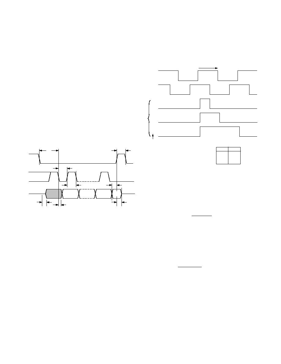
CS can be released a minimum of 100 ns after the last negative
edge. If the user is reading data continuously,
CS can be reap-
plied a minimum of 250 ns after it is released (see Figure 6).
The maximum read time is given by: (12-bits read @ 2 MHz)
Max RD Time = [600 + (12
×
500) + 600 + 100] = 7.30
µ
s.
INCREMENTAL ENCODER OUTPUTS
The incremental encoder emulation outputs A, B and NM are
free running and are always valid, providing that valid resolver
format input signals are applied to the converter.
The AD2S90 emulates a 1024-line encoder. Relating this to
converter resolution means one revolution produces 1024 A, B
pulses. B leads A for increasing angular rotation (i.e., clockwise
direction). The addition of the DIR output negates the need for
external A and B direction decode logic. DIR is HI for increas-
ing angular rotation.
The north marker pulse is generated as the absolute angular
position passes through zero. The AD2S90 supports the three
industry standard widths controlled using the NMC pin. Figure
7 details the relationship between A, B and NM. The width of
NM is defined relative to the A cycle.
A
B
90
180
*
NM
NUMBER OF DEGREES REFERS TO WIDTH RELATIVE TO "A" CYCLE
360
SELECTABLE WITH THREE - LEVEL
CONTROL PIN "MARKER" DEFAULT
TO 90 USING INTERNAL PULL - UP.
*
WIDTH
LEVEL
90
180
360
+V
DD
0
V
SS
INCREASING ANGLE
Figure 7. A, B and NM Timing
Unlike incremental encoders, the AD2S90 encoder output is
not subject to error specifications such as cycle error, eccentric-
ity, pulse and state width errors, count density and phase
.
The maximum speed rating, n, of an encoder is calculated from
its maximum switching frequency, f
MAX
, and its ppr (pulses per
revolution).
n
=
60
×
f
MAX
PPR
The AD2S90 A, B pulses are initiated from CLKOUT which
has a maximum frequency of 2.048 MHz. The equivalent
encoder switching frequency is:
1/4
×
2.048 MHz = 512 kHz (4 updates = 1 pulse)
At 12 bits the ppr = 1024, therefore the maximum speed, n, of
the AD2S90 is:
n
rpm
=
×
=
60
512000
1024
30000
This compares favorably with encoder specifications where f
MAX
is specified from 20 kHz (photo diodes) to 125 kHz (laser based)
depending on the light system used. A 1024 line laser-based
encoder will have a maximum speed of 7300 rpm.
The inclusion of A, B outputs allows the AD2S90 + resolver
solution to replace optical encoders directly without the need to
change or upgrade existing application software.
AD2S90
REV. D
7
VELOCITY OUTPUT
The analog velocity output VEL is scaled to produce 150 rps/V
dc
±
15%. The sense is positive V dc for increasing angular
rotation. VEL can drive a maximum load combination of
10 k
and 30 pF. The internal velocity scaling is fixed.
POSITION CONTROL
The rotor movement of dc or ac motors used for servo control is
monitored at all times. Feedback transducers used for this pur-
pose detect either relative position in the case of an incremental
encoder or absolute position and velocity using a resolver. An
incremental encoder only measures change in position not
actual position.
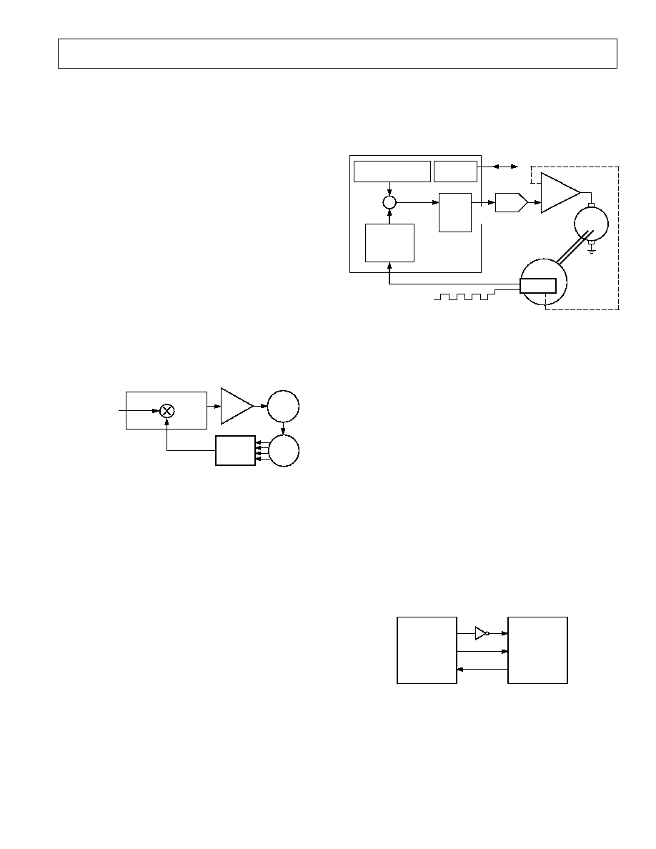
Closed Loop Control Systems
The primary demand for a change in position must take into
account the magnitude of that change and the associated accel-
eration and velocity characteristics of the servo system. This is
necessary to avoid "hunting" due to over- or underdamping of
the control employed.
A position loop needs both actual and demand position infor-
mation. Algorithms consisting of proportional, integral and
derivative control (PID) may be implemented to control the
velocity profile.
A simplified position loop is shown in Figure 8.
POSITION
DEMAND
POSITION CONTROLLER
RE-
SOLVER
ACTUAL
POSITION
SERVO
MOTOR
AD2S90
SERVO
AMP
Figure 8. Position Loop
MOTION CONTROL PROCESSES
Advanced VLSI designs mean that silicon system blocks are now
available to achieve high performance motion control in servo
systems.
A digital position control system using the AD2S90 is shown in
Figure 9. In this system the task of determining the acceleration
and velocity characteristics is fulfilled by programming a trap-
ezoidal velocity profile via the I/O port.
As can be seen from Figure 9 encoder position feedback infor-
mation is used. This is a popular format and one which the
AD2S90 emulates thereby facilitating the replacement of encod-
ers with an AD2S90 and a resolver. However, major benefits
can be realized by adopting the resolver principle as opposed to
the incremental technique.
Incremental feedback based systems normally carry out a peri-
odic check between the position demanded by the controller
and the increment position count. This requires software and
hardware comparisons and battery backup in the case of power
failure. If there is a supply failure and the drive system moves,
unless all parts of the system are backed up, a reset to a known
datum point needs to take place. This can be extremely hazard-
ous in many applications. The AD2S90 gets round this problem
by supplying an absolute position serial data stream upon re-
quest, thus removing the need to reset to a known datum.
INCREMENTAL POSITION
+
RESOLVER
OPTIONAL
VELOCITY
FEEDBACK
HOST I/O
PORT
TO HOST PROCESSOR
ABSOLUTE
POSITION
HOST
INTERFACE
COMMAND POSITION
SEQUENCER (32-BIT)
POSITION
FEEDBACK
PROCESSOR
(32-BIT)
IN
, A, B
AD2S90
DC
MOTOR
DAC
PORT
DIGITAL
PID
FILTER
(16-BIT)
8 12
DAC
POWER
AMP
Figure 9. Practical Implementation of the AD2S90
DSP Interfacing
The AD2S90 serial output is ideally suited for interfacing to
DSP configured microprocessors. Figures 10 to 13 illustrate
how to configure the AD2S90 for serial interfacing to the DSP.
ADSP-2105 Interfacing
Figure 10 shows the AD2S90 interfaced to an ADSP-2105. The
on-chip serial port of the ADSP-2105 is used in alternate fram-
ing receive mode with internal framing (internally inverted) and
internal serial clock generation (externally inverted) options
selected. In this mode the ADSP-2105 provides a
CS and a
serial clock to the AD2S90. The serial clock is inverted to pre-
vent timing errors as a result of both the AD2S90 and ADSP-
2105 clock data on the negative edge of SCLK. The first data
bit is void; 12 bits of significant data then follow on each con-
secutive negative edge of the clock. Data is clocked from the
AD2S90 into the data receive register of the ADSP-2105. This
is internally set to 13 bit (12 bits and one "dummy" bit) when
13 bits are received. The serial port automatically generates an
internal processor interrupt. This allows the ADSP-2105 to read
12 significant bits at once and continue processing.
The ADSP-2101, ADSP-2102, ADSP-2111 and 21msp50 can
all interface to the AD2S90 with similar interface circuitry.
SCLK
RFS
DR
SCLK
CS
DATA
ADSP-2105
AD2S90
NOTE:
ADDITIONAL PINS OMITTED FOR CLARITY
Figure 10. ADSP-2105/AD2S90 Serial Interface
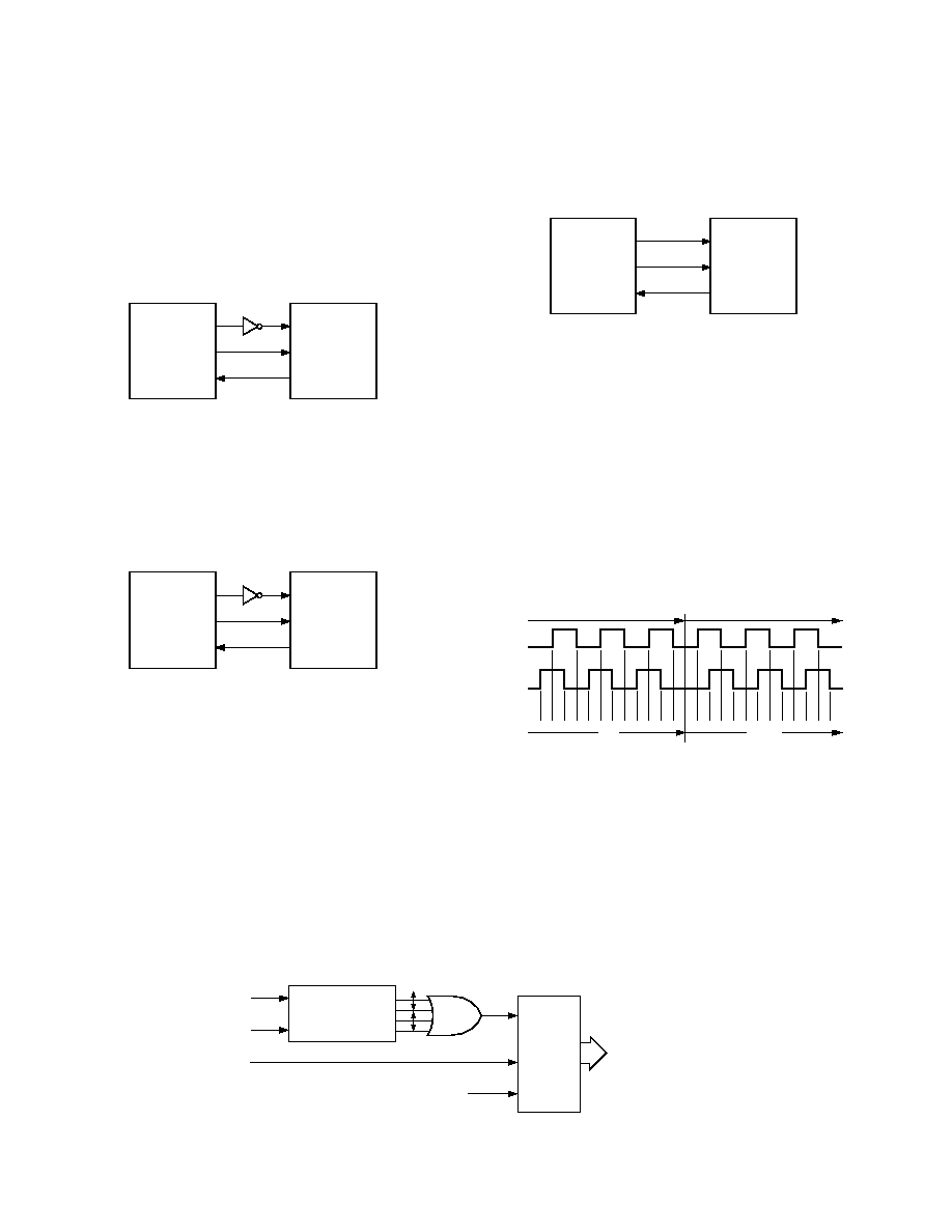
AD2S90
REV. D
8
Select the AD2S90 and frame the data. The S1 register is fixed
at 16 bits, therefore, to obtain the 12-significant bits the proces-
sor needs to execute four right shifts. Once the NEC7720 has
read 16 bits, an internal interrupt is generated to read the inter-
nal contents of the S1 register.
SCLK
SIEN
S1
SCLK
CS
DATA
PD7720
AD2S90
NOTE:
ADDITIONAL PINS OMITTED FOR CLARITY
Figure 13.
µ
PD7720/AD2S90 Serial Interface
EDGE TRIGGERED 4 DECODING LOGIC
In most data acquisition or control systems the A, B incremental
outputs must be decoded into absolute information, normally a
parallel word, before they can be utilized effectively.
To decode the A, B outputs on the AD2S90 the user must
implement a 4
×
decoding architecture. The principle states that
one A, B cycle represents 4 LSB weighted increments of the
converter (see Equation 4).
Up = (
A) · B + (
B) · A + (
A) ·
B + (
) ·
A
Down = (
A) ·
B + (
B) · A + (
A) · B + (
B) ·
A
(4)
CLOCKWISE ROTATION
COUNTER CLOCKWISE ROTATION
UP
DOWN
CH A
CH B
Figure 14. Principles of 4
×
Decoding
The algorithms in Equation 4 can be implemented using the
architecture shown in Figure 15. Traditionally the direction of
the shaft is decoded by determining whether A leads B. The
AD2S90 removes the need to derive direction by supplying a
direction output state which can be fed straight into the up-
down counter.
For further information on this topic please refer to the applica-
tion note "Circuit Applications of the AD2S90 Resolver-to-
Digital Converters."
TMS32020 Interfacing
Figure 11 shows the serial interface between the AD2S90 and
the TMS32020. The interface is configured in alternate internal
framing, external clock (externally inverted) mode. Sixteen bits
of data are clocked from the AD2S90 into the data receive regis-
ter (DRR) of the TMS32020. The DRR is fixed at 16 bits. To
obtain the 12-significant bits, the processor needs to execute
three right shifts. (First bit read is void, the last three will be
zeros). When 16 bits have been received by the TMS32020, it
generates an internal interrupt to read the data from the DRR.
SCLK
FSR
DRR
SCLK
CS
DATA
TMS32020
AD2S90
NOTE:
ADDITIONAL PINS OMITTED FOR CLARITY
Figure 11. TMS32020/AD2S90 Serial Interface
DSP56000 Interface
Figure 12 shows a serial interface between the AD2S90 and the
DSP56000. The DSP in configured for normal mode synchro-
nous operation with gated clock with SCLK and SC1 as out-
puts. SC1 is applied to
CS.
SCLK
SC1
SRD
SCLK
CS
DATA
DSP56000
AD2S90
NOTE:
ADDITIONAL PINS OMITTED FOR CLARITY
Figure 12. DSP56000/AD2S90 Serial Interface
The DSP56000 assumes valid data on the first falling edge of
SCLK. SCLK is inverted to ensure that the valid data is clocked
in after one leading bit. The receive data shift register (SRD) is
set for a 13-bit word.
When this register has received 13 bits of data, it generates an
internal interrupt on the DSP56000 to read the 12 bits of sig-
nificant data from the register.
NEC7720 Interface
Figure 13 shows the serial interface between the NEC7720 and
the AD2S90. The NEC7720 expects data on the rising edge of
its SCLK output, and therefore unlike the previous interfaces no
inverter is required to clock data into the S1 register. There is
no need to ignore the first data bit read.
SIEN is used to Chip
EDGE GENERATOR
A
A
B
B
CHA
CHB
DIRECTION
CLOCK
U/D
RESET
UP/DOWN
COUNTER
PARALLEL
DIGITAL
OUTPUT
Figure 15. 4
×
Decoding Incremental to Parallel Conversion
AD2S90
REV. D
9
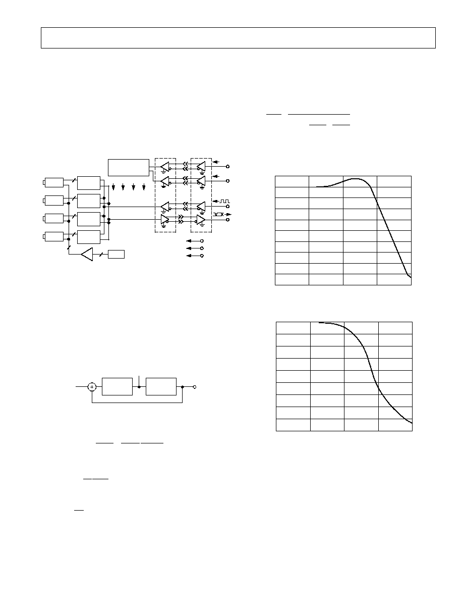
REMOTE MULTIPLE SENSOR INTERFACING
The DATA output of the AD2S90 is held in a high impedance
state until
CS is taken LO. This allows a user to operate the
AD2S90 in an application with more than one converter con-
nected on the same line. Figure 16 shows four resolvers inter-
faced to four AD2S90s. Excitation for the resolvers is provided
locally by an oscillator.
SCLK, DATA and two address lines are fed down low loss
cables suitable for communication links. The two address lines
are decoded locally into
CS for the individual converters. Data
is received and transmitted using transmitters and receivers.
2-4 DECODING
(74HC139)
CS
1
CS
2
CS
3
CS
4
A0
A1
SCLK
DATA
V
DD
V
SS
0V
AD2S90
1
RES1
AD2S90
2
RES2
AD2S90
3
RES3
AD2S90
4
RES4
4
4
4
4
2
2
OSC
BUFFER
Figure 16. Remote Sensor Interfacing
CIRCUIT DYNAMICS/ERROR SOURCES
Transfer Function
The AD2S90 operates as a Type 2 tracking servo loop. An
integrator and VCO/counter perform the two integrations inher-
ent in a Type 2 loop.
The overall system response of the AD2S90 is that of a unity
gain second order low-pass filter, with the angle of the resolver
as the input and the digital position data as the output. Figure
17 illustrates the AD2S90 system diagram.
A2 (S)
A1 (S)
IN
VEL OUT
OUT
Figure 17. AD2S90 Transfer Function
The open-loop transfer function is given by:
OUT
IN
=
K
1
K
2
s
2
(1
+
st
1
)
1
+
st
2
(5)
where:
A s
K
s
st
st
1
1
1
2
1
1
( )
=
+
+
t
ms
t
s
1
2
1 0
90
=
=
.
µ
(6)
A s
K
s
K
V
LSB
K
LSB V
2
2
1
2
4 875
614 400
( )
.
/(
sec)
,
/(
sec)
=
=
×
=
×
(7)
The AD2S90 acceleration constant is given by:
K
K
K
a
=
×
×
-
1
2
6
2
3 0 10
.
sec
(8)
The AD2S90's design has been optimized with a critically
damped response. The closed-loop transfer function is given by:
OUT
IN
st
st
s
K K
s t
K K
=
+
+ +
+
1
1
1
1
2
1
2
3
2
1
2
(9)
The normalized gain and phase diagrams are given in Figures 18
and 19.
5
45
30
40
10
35
1
15
25
20
10
5
0
1k
100
FREQUENCY Hz
10k
Figure 18. AD2S90 Gain Plot
FREQUENCY Hz
0
180
10k
140
160
10
1
120
100
80
60
40
20
1k
100
Figure 19. AD2S90 Phase Plot
AD2S90
REV. D
10
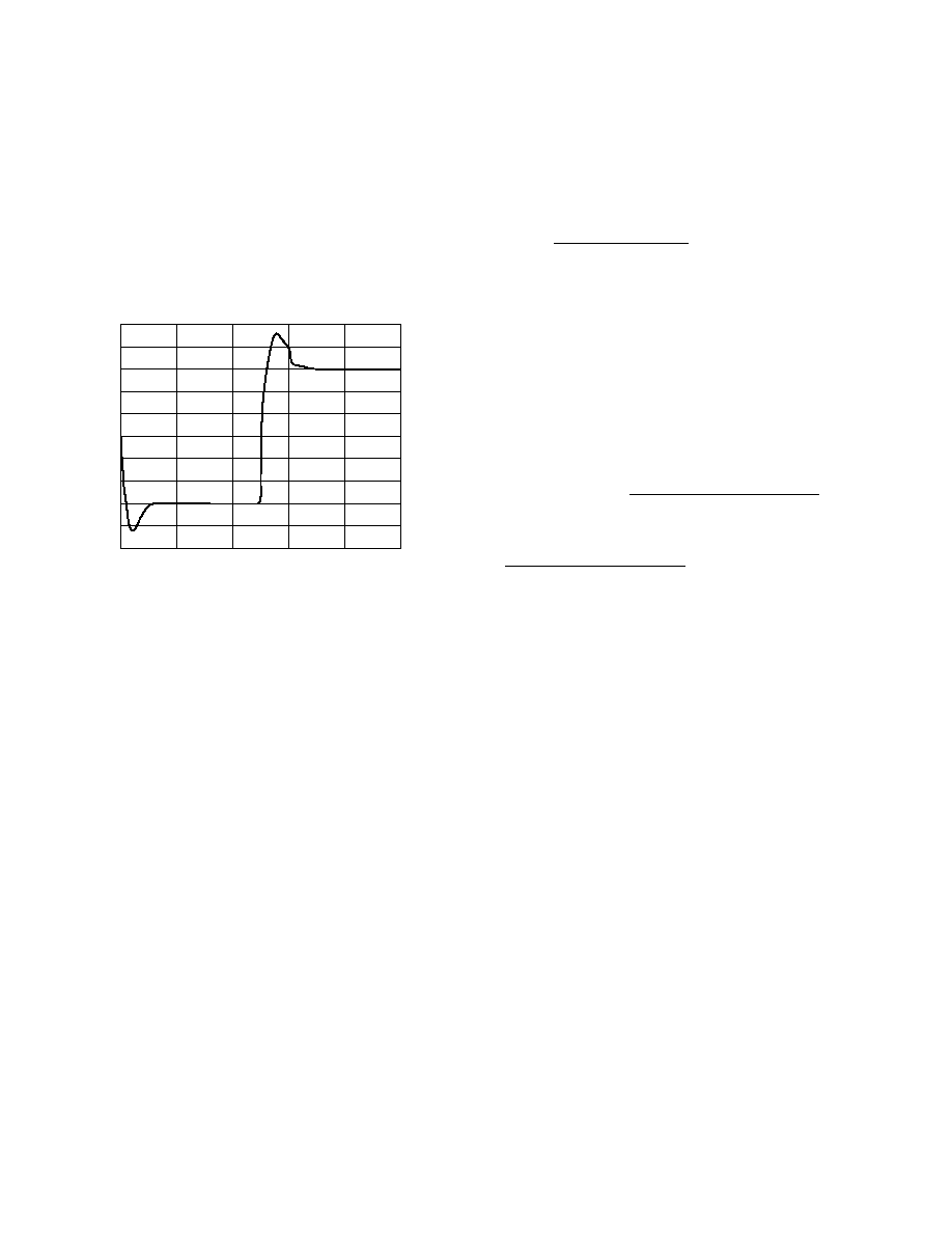
The small step response is given in Figure 20, and is the time
taken for the converter to settle to within 1 LSB.
ts = 7.00 ms (maximum)
The large step response (steps >20
°
) applies when the error
voltage will exceed the linear range of the converter. Typically it
will take three times longer to reach the first peak for a 179
°
step.
In response to a velocity step [VELOUT/(d
/dt)] the velocity
output will exhibit the same response characteristics as outlined
above.
0
10
DEGREES
20
0
16
4
8
12
Figure 20. Small Step Response
SOURCES OF ERROR
Acceleration Error
A tracking converter employing a Type 2 servo loop does not
suffer any velocity lag, however, there is an additional error due
to acceleration. This additional error can be defined using the
acceleration constant K
a
of the converter.
K
a
=
Input Acceleration
Error in Output Angle
(10)
The numerator and denominator's units must be consistent. K
a
does not define maximum input acceleration, only the error due to
its acceleration. The maximum acceleration allowable before the
converter loses track is dependent on the angular accuracy
requirements of the system.
Angular Error
×
K
a
= degrees/sec
2
(11)
K
a
can be used to predict the output position error for a given
input acceleration. The AD2S90 has a fixed K
a
= 3.0
×
10
6
sec
2
if we apply an input accelerating at 100 revs/sec
2
, the error
can be calculated as follows:
Error in LSBs
=
Input Acceleration LSB / sec
2
[
]
K
a
sec
-
2
[ ]
=
[
]
×
[
]
×
[ ]
=
100
2
3 0 10
0 14
12
6
2
rev
LSB rev
LSBs
/
/
.
sec
.
sec
2
(12)
AD2S90
REV. D
11
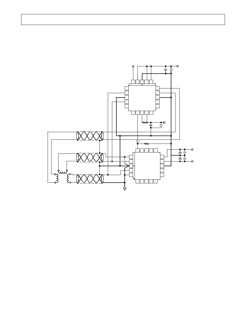
AD2S90/AD2S99 TYPICAL CONFIGURATION
Figure 21 shows a typical circuit configuration for the AD2S99
Oscillator and the AD2S90 Resolver-to-Digital Converter. The
maximum level of the SIN and COS input signals to the
AD2S90 should be 2 V rms
±
10%. All the analog ground sig-
nals should be star connected to the AD2S90 AGND pin. If
shielded twisted pair cables are used for the resolver signals, the
shields should also be terminated at the AD2S90 AGND pin.
The SYNREF output of the AD2S99 should be connected to
the REF input pin of the AD2S90 via a 0.1
µ
F capacitor with a
100 k
resistor to GND. This is to block out any dc offset in
the SYNREF signal. For more detailed information please refer
to the AD2S99 data sheet.
NC = NO CONNECT
NC
SIN
NC
DGND
COS
EXC
EXC
NC
AGND
NC
3
1
2
4
5
8
6
7
17
14
16
15
TOP VIEW
(Not to Scale)
AD2S99
F
BIAS
SEL1
V
SS
SEL2
V
SS
NC
SYNREF
NC
LOS
V
DD
19
3
1
2
20
4
5
8
6
7
12
13
9
11
10
18 17
14
16 15
4.7 F
4.7 F
0.1 F
0.1 F
COS
SIN
REF
S2
S4
S3
S1
R4
R2
RESOLVER
REF
COS
AGND
SIN
SIN LO
V
DD
V
SS
DGND
AD2S90
TOP VIEW
(Not to Scale)
0.1 F
100k
V
DD
V
SS
V
DD
0.1 F
50k
4.7 F
0.1 F
4.7 F
V
SS
SEL2 = GND
SEL1 = V
SS
F
OUT
= 5kHz
COS LO
20 19
18
9
10 11 12 13
Figure 21. AD2S90 and AD2S99 Example Configuration
AD2S90
REV. D
12
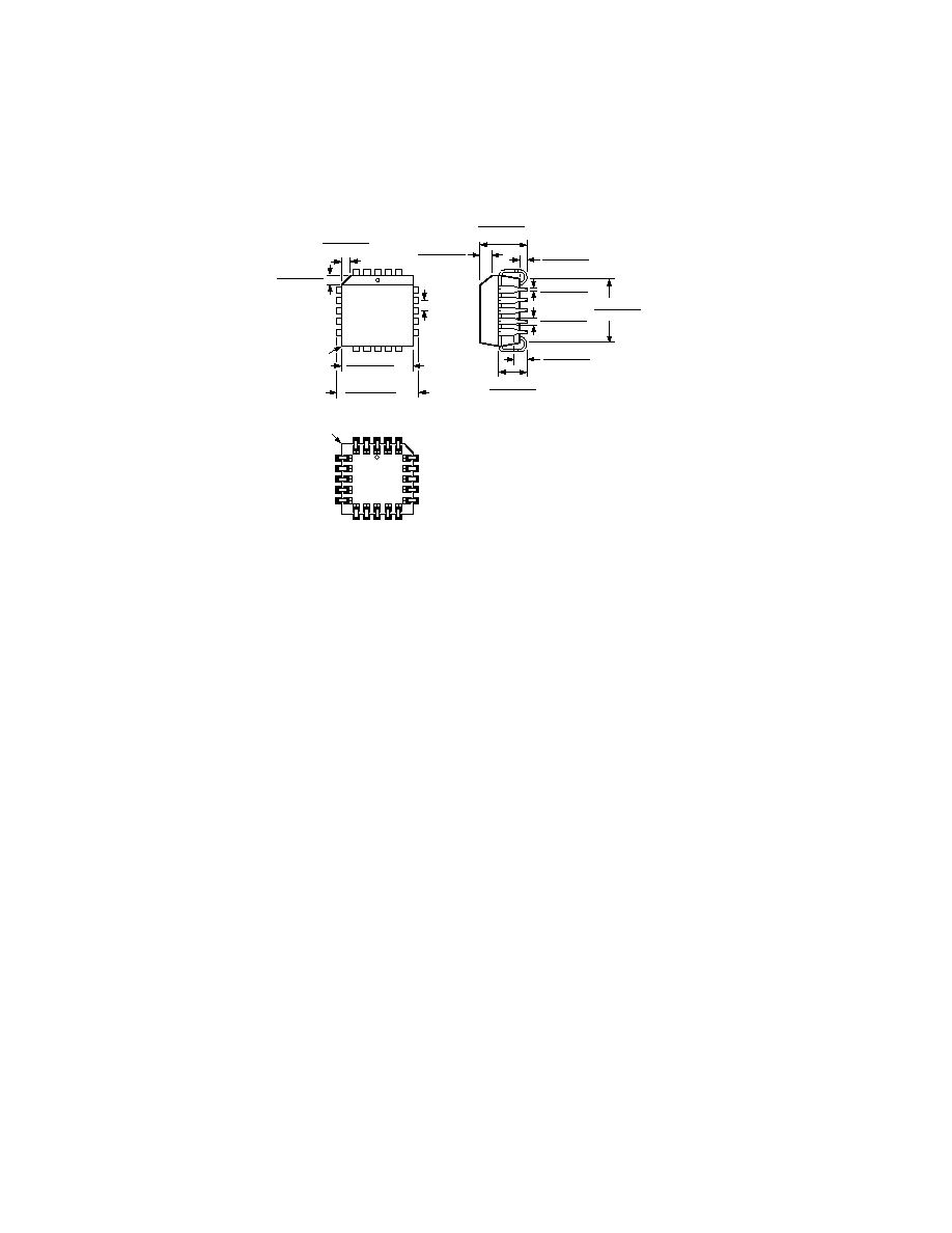
OUTLINE DIMENSIONS
Dimensions shown in inches and (mm).
P-20A
20-Lead Plastic Leaded Chip Carrier (PLCC)
PIN 1
IDENTIFIER
BOTTOM
VIEW
(PINS UP)
0.020
(0.50)
R
0.021 (0.53)
0.013 (0.33) 0.330 (8.38)
0.290 (7.37)
0.032 (0.81)
0.026 (0.66)
0.180 (4.57)
0.165 (4.19)
0.040 (1.01)
0.025 (0.64)
0.056 (1.42)
0.042 (1.07)
0.025 (0.63)
0.015 (0.38)
0.110 (2.79)
0.085 (2.16)
3
PIN 1
IDENTIFIER
4
19
18
8
9
14
13
TOP VIEW
(PINS DOWN)
0.395 (10.02)
0.385 (9.78)
SQ
0.356 (9.04)
0.350 (8.89)
SQ
0.048 (1.21)
0.042 (1.07)
0.048 (1.21)
0.042 (1.07)
0.020
(0.50)
R
0.050
(1.27)
BSC
C1653b21/99
PRINTED IN U.S.A.