 | ÐлекÑÑоннÑй компоненÑ: AD2S83 | СкаÑаÑÑ:  PDF PDF  ZIP ZIP |
Äîêóìåíòàöèÿ è îïèñàíèÿ www.docs.chipfind.ru
REV. D
Information furnished by Analog Devices is believed to be accurate and
reliable. However, no responsibility is assumed by Analog Devices for its
use, nor for any infringements of patents or other rights of third parties
which may result from its use. No license is granted by implication or
otherwise under any patent or patent rights of Analog Devices.
a
Variable Resolution,
Resolver-to-Digital Converter
AD2S83
GENERAL DESCRIPTION
The AD2S83 is a monolithic 10-, 12-, 14- or 16-bit tracking
resolver-to-digital converter.
The converter allows users to select their own resolution and dy-
namic performance with external components. The converter allows
users to select the resolution to be 10, 12, 14 or 16 bits and to
track resolver signals rotating at up to 1040 revs per second
(62,400 rpm) when set to 10-bit resolution.
The AD2S83 converts resolver format input signals into a paral-
lel natural binary digital word using a ratiometric tracking con-
version method. This ensures high noise immunity and tolerance of
long leads allowing the converter to be located remote from the
resolver.
The position output from the converter is presented via 3-state
output pins which can be configured for operations with 8- or
16-bit bus. BYTE SELECT,
ENABLE and INHIBIT pins
ensure easy data transfer to 8- and 16-bit data bus, and outputs
are provided to allow for cycle or pitch counting in external
counters.
A precise analog signal proportional to velocity is also available
and will replace a tachogenerator.
The AD2S83 operates over reference frequencies in the range
0 Hz to 20,000 Hz.
PRODUCT HIGHLIGHTS
High Accuracy Velocity Output. A precision analog velocity
signal with a typical linearity of
±
0.1% and reversion error less
than
±
0.3% is generated by the AD2S83. The provision of this
signal removes the need for mechanical tachogenerators used in
servo systems to provide loop stabilization and speed control.
Resolution Set by User. Two control pins are used to select
the resolution of the AD2S83 to be 10, 12, 14 or 16 bits allow-
ing optimum resolution for each application.
Ratiometric Tracking Conversion. This technique provides
continuous output position data without conversion delay. It
also provides noise immunity and tolerance of harmonic distor-
tion on the reference and input signals.
Dynamic Performance Set by the User. By selecting exter-
nal resistor and capacitor values the user can determine band-
width, maximum tracking rate and velocity scaling of the
converter to match the system requirements. The component
values are easy to select using the free component selection
software design aid.
MODELS AVAILABLE
Information on the models available is given in the Ordering
Guide.
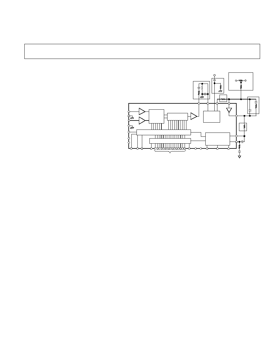
FUNCTIONAL BLOCK DIAGRAM
FEATURES
Tracking R/D Converter
High Accuracy Velocity Output
High Max Tracking Rate 1040 RPS (10 Bits)
44-Lead PLCC Package
10-, 12-, 14- or 16-Bit Resolution Set by User
Ratiometric Conversion
Stabilized Velocity Reference
Dynamic Performance Set by User
Industrial Temperature Range
APPLICATIONS
DC and AC Servo Motor Control
Process Control
Numerical Control of Machine Tools
Robotics
Axis Control
One Technology Way, P.O. Box 9106, Norwood, MA 02062-9106, U.S.A.
Tel: 781/329-4700
World Wide Web Site: http://www.analog.com
Fax: 781/326-8703
© Analog Devices, Inc., 1998
A3
RIPPLE
CLOCK
R4
VCO
I/P
TRACKING
RATE
SELECTION
R6
VELOCITY
SIGNAL
INTEGRATOR
I/P
BANDWIDTH
SELECTION
R3
C3
REFERENCE
I/P
HF FILTER
R2
C2
C1
R1
DEMOD
O/P
INTEGRATOR
O/P
DIRECTION
BUSY
DIG
GND
16
DATA BITS
SC1 SC2
DATA
LOAD
BYTE
SELECT
+5V
+12V
12V
GND
COS
SIG
GND
SIN
AC ERROR O/P
VCO
O/P
C7
AD2S83
R7
3K3
C6
390pF
R8
12V
+12V
OFFSET ADJUST
R9
R5
C4
C5
R 2R DAC
PHASE
SENSITIVE
DETECTOR
VCO + DATA
TRANSFER
LOGIC
16-BIT UP/DOWN COUNTER
SEGMENT
SWITCHING
OUTPUT DATA LATCH
A2
A1
ENABLE
INHIBIT

AD2S83SPECIFICATIONS
AD2S83
Parameter
Conditions
Min
Typ
Max
Units
SIGNAL INPUTS (SIN, COS)
Frequency
1
0
20,000
Hz
Voltage Level
1.8
2.0
2.2
V rms
Input Bias Current
60
150
nA
Input Impedance
1.0
M
REFERENCE INPUT (REF)
Frequency
0
20,000
Hz
Voltage Level
1.0
8.0
V pk
Input Bias Current
60
150
nA
Input Impedance
1.0
M
PERFORMANCE
Repeatability
1
LSB
Allowable Phase Shift
(Signals to Reference)
10
+10
Degree
Max Tracking Rate
10 Bits
1040
rps
12 Bits
260
rps
14 Bits
65
rps
16 Bits
16.25
rps
Bandwidth
User Selectable
ACCURACY
Angular Accuracy
A, I
8 +1 LSB
arc min
Monotonicity
Guaranteed Monotonic
Missing Codes (16-Bit Resolution)
A, I
4
Codes
VELOCITY SIGNAL
LINEARITY
2, 3, 4
AD2S83AP
0 kHz500 kHz
40
°
C to +85
°
C
±
0.15
0.25
% FSR
0.5 MHz1 MHz
40
°
C to +85
°
C
±
0.25
1.0
% FSR
AD2S83IP
0 kHz500 kHz
40
°
C to +85
°
C
±
0.25
0.5
% FSR
0.5 MHz1 MHz
40
°
C to +85
°
C
±
0.25
1.0
% FSR
Reversion Error
AD2S83AP
40
°
C to +85
°
C
±
0.5
1.0
% O/P
AD2S83IP
40
°
C to +85
°
C
±
1.0
1.5
% O/P
DC Zero Offset
5
±
3
mV
Gain Scaling Accuracy
±
1.5
3
% FSR
Output Voltage
1 mA Load
±
8
V
Dynamic Ripple
Mean Value
1.0
% rms O/P
INPUT/OUTPUT PROTECTION
Analog Inputs
Overvoltage Protection
±
8
V
Analog Outputs
Short Circuit O/P Protection
±
5.6
±
8
±
10.4
mA
DIGITAL POSITION
Resolution
10, 12, 14, and 16
Bits
Output Format
Bidirectional Natural Binary
Load
3
LSTTL
INHIBIT
6
Sense
Logic LO to
INHIBIT
Time to Stable Data
240
390
490
ns
ENABLE
6
Logic LO Enables Position Output
Logic HI Outputs in High
ENABLE
6
/Disable Time
Impedance State
35
110
ns
BYTE SELECT
6
Sense
Logic HI
MS Byte DB1DB8
Logic LO
LS Byte DB1DB8
Time to Data Available
60
140
ns
SHORT CYCLE INPUTS
Internally Pulled High via
100 k
to +V
S
SC1
SC2
0
0
10-Bit Resolution
0
1
12-Bit Resolution
1
0
14-Bit Resolution
1
1
16-Bit Resolution
( V
S
= 12 V dc 5%; V
L
= +5 V dc
10%; T
A
= 40 C to +85 C)
2
REV. D

AD2S83
Parameter
Conditions
Min
Typ
Max
Units
COMPLEMENT
Internally Pulled High via 100 k
to +V
S
. Logic LO to Activate;
No Connect for Normal Operation
DATA LOAD
Sense
Internally Pulled High via 100 k
150
300
ns
to +V
S
. Logic LO Allows
Data to be Loaded into the
Counters from the Data Lines
BUSY
6, 7
Sense
Logic HI When Position O/P Changing
Width
150
350
ns
Load
Use Additional Pull-Up (See Figure 2)
1
LSTTL
DIRECTION
6
Sense
Logic HI Counting Up
Logic LO Counting Down
Max Load
3
LSTTL
RIPPLE CLOCK
6
Sense
Logic HI
All 1s to All 0s
All 0s to All 1s
Width
Dependent on Input Velocity
300
ns
Reset
Before Next Busy
Load
3
LSTTL
DIGITAL INPUTS
Input High Voltage, V
IH
INHIBIT, ENABLE
2.0
V
DB1DB16, Byte Select
±
V
S
=
±
11.4 V, V
L
= 5.0 V
Input Low Voltage, V
IL
INHIBIT, ENABLE
0.8
V
DB1DB16, Byte Select
±
V
S
=
±
12.6 V, V
L
= 5.0 V
DIGITAL INPUTS
Input High Current, I
IH
INHIBIT, ENABLE
100
µ
A
DB1DB16
±
V
S
=
±
12.6 V, V
L
= 5.5 V
Input Low Current, I
IL
INHIBIT, ENABLE
100
µ
A
DB1DB16, Byte Select
±
V
S
=
±
12.6 V, V
L
= 5.5 V
DIGITAL INPUTS
Low Voltage, V
IL
ENABLE = HI
1.0
V
SC1, SC2,
DATA LOAD
±
V
S
=
±
12.0 V, V
L
= 5.0 V
Low Current, I
IL
ENABLE = HI
400
µ
A
SC1, SC2,
DATA LOAD
±
V
S
=
±
12.0 V, V
L
= 5.0 V
DIGITAL OUTPUTS
High Voltage, V
OH
DB1DB16
2.4
V
RIPPLE CLK, DIR
±
V
S
=
±
12.0 V, V
L
= 4.5 V
I
OH
= 100
µ
A
Low Voltage, V
OL
DB1DB16
0.4
V
RIPPLE CLK, DIR
±
V
S
=
±
12.0 V, V
L
= 5.5 V
I
OL
= 1.2 mA
NOTES
1
Angular accuracy is not guaranteed <50 Hz reference frequency.
2
Linearity derates from 500 kHz1000 kHz @ 0.0017%/kHz.
3
Refer to Definition of Linearity, "The AD2S83 as a Silicon Tachogenerator."
4
Worst case reversion error at temperature extremes.
5
Velocity output offset dependent on value for R6.
6
Refer to timing diagram.
7
Busy pulse guaranteed up to a VCO rate of 900 kHz.
All min and max specifications are guaranteed. Specifications in boldface are tested on all production units at final electrical test.
Specifications subject to change without notice.
AD2S83
3
REV. D

AD2S83SPECIFICATIONS
AD2S83
Parameter
Conditions
Min
Typ
Max
Units
THREE-STATE LEAKAGE
DB1DB16 Only
Current I
L
±
V
S
=
±
12.0 V, V
L
= 5.5 V
20
µ
A
V
OL
= 0 V
±
V
S
=
±
12.0 V, V
L
= 5.5 V
20
µ
A
V
OH
= 5.0 V
RATIO MULTIPLIER
AC Error Output Scaling
10 Bit
177.6
mV/Bit
12 Bit
44.4
mV/Bit
14 Bit
11.1
mV/Bit
16 Bit
2.775
mV/Bit
PHASE SENSITIVE DETECTOR
Output Offset Voltage
12
mV
Gain
In Phase
w.r.t. REF
0.882
0.9
0.918
V rms/V dc
In Quadrature
w.r.t. REF
±
0.02
V rms/V dc
Input Bias Current
60
150
nA
Input Impedance
1.0
M
Input Voltage
±
8
V
INTEGRATOR
Open-Loop Gain
At 10 kHz
57
60
63
dB
Dead Zone Current (Hysteresis)
90
100
110
nA/LSB
Input Offset Voltage
1
5
mV
Input Bias Current
60
150
nA
Output Voltage Range
8
V
VCO
Maximum Rate
1.1
MHz
VCO Rate
+ve DIR
8.25
8.50
8.75
kHz/
µ
A
ve DIR
8.25
8.50
8.75
kHz/
µ
A
VCO Power Supply Sensitivity
Rate
+V
S
+0.5
%/V
V
S
0.5
%/V
Input Offset Voltage
3
mV
Input Bias Current
12
50
nA
Input Bias Current Tempco
+0.22
nA/
°
C
Linearity of Absolute Rate
AD2S83AP
0 kHz500 kHz
±
0.15
0.25
% FSR
0.5 MHz1 MHz
±
0.25
1.0
% FSR
AD2S83IP
0 kHz500 kHz
±
0.25
0.5
% FSR
0.5 MHz1 MHz
±
0.25
1.0
% FSR
Reversion Error
AD2S83AP
±
0.5
1.0
% Output
AD2S83IP
±
1.0
1.5
% Output
POWER SUPPLIES
Voltage Levels
+V
S
+11.4
+12.6
V
V
S
11.4
12.6
V
+V
L
+4.5
+5
+V
S
V
Current
±
I
S
±
V
S
@
±
12 V
±
12
23
mA
±
I
S
±
V
S
@
±
12.6 V
±
19
30
mA
±
I
L
+V
L
@
±
5.0 V
±
0.5
1.5
mA
All min and max specifications are guaranteed. Specifications in boldface are tested on all production units at final electrical test.
Specification subject to change without notice.
( V
S
= 12 V dc 5%; V
L
= +5 V dc
10%; T
A
= 40 C to +85 C)
ORDERING GUIDE
Temperature
Package
Package
Model
Range
Accuracy
Description
Option
AD2S83AP
40
°
C to +85
°
C
8 arc min
Plastic Leaded Chip Carrier
P-44A
AD2S83IP
40
°
C to +85
°
C
8 arc min
Plastic Leaded Chip Carrier
P-44A
REV. D
4
AD2S83
5
REV. D
PIN FUNCTION DESCRIPTIONS
P
in
Nos.
Mnemonic
Description
1
DEMOD O/P
Demodulator Output
2
REFERENCE I/P
Reference Signal Input
3
AC ERROR O/P
Ratio Multiplier Output
4
COS
Cosine Input
5
ANALOG GND
Power Ground
6
SIGNAL GND
Resolver Signal Ground
7
SIN
Sine Input
8
+V
S
Positive Power Supply
1025 DB1DB16
Parallel Output Data
26
+V
L
Logic Power Supply
27
ENABLE
Logic HI--Output Data Pins in
High Impedance State
Logic LO--Presents Active Data
to the Output Pins
28
BYTE SELECT
Logic HI--Most Significant Byte to
DB1DB8
Logic LO--Least Significant Byte
to DB1DB8
30
INHIBIT
Logic LO Inhibits Data Transfer
to Output Latches
31
DIGITAL GND
Digital Ground
32, 33 SC2SC1
Select Converter Resolution
34
DATA LOAD
Logic LO DB1DB16 Inputs
Logic HI DB1DB16 Outputs
35
COMPLEMENT
Active Logic LO
36
BUSY
Converter Busy, Data not Valid
While Busy HI
37
DIRECTION
Logic State Defines Direction of
Input Signal Rotation
38
RIPPLE CLOCK
Positive Pulse When Converter Output
Changes from 1s to All 0s or Vice Versa
39
V
S
Negative Power Supply
40
VCO I/P
VCO Input
41
VCO O/P
VCO Output
42
INTEGRATOR O/P
Integrator Output
43
INTEGRATOR I/P
Integrator Input
44
DEMOD I/P
Demodulator Input
ABSOLUTE MAXIMUM RATINGS
1
(with respect to GND)
+V
S
2
. . . . . . . . . . . . . . . . . . . . . . . . . . . . . . . . . . . . . +13 V dc
V
S
2
. . . . . . . . . . . . . . . . . . . . . . . . . . . . . . . . . . . . . 13 V dc
+V
L
. . . . . . . . . . . . . . . . . . . . . . . . . . . . . . . . . . . . . . . . . . +V
S
Reference . . . . . . . . . . . . . . . . . . . . . . . . . . . . . . . +13 V to V
S
SIN . . . . . . . . . . . . . . . . . . . . . . . . . . . . . . . . . . . +13 V to V
S
COS . . . . . . . . . . . . . . . . . . . . . . . . . . . . . . . . . . +13 V to V
S
Any Logical Input . . . . . . . . . . . . . . . . . . 0.4 V dc to +V
L
dc
Demodulator Input . . . . . . . . . . . . . . . . . . . . . . . +13 V to V
S
Integrator Input . . . . . . . . . . . . . . . . . . . . . . . . . . +13 V to V
S
VCO Input . . . . . . . . . . . . . . . . . . . . . . . . . . . . . +13 V to V
S
Power Dissipation . . . . . . . . . . . . . . . . . . . . . . . . . . . 800 mW
Operating Temperature
Industrial (AP, IP) . . . . . . . . . . . . . . . . . . . 40
°
C to +85
°
C
Storage Temperature . . . . . . . . . . . . . . . . . . 65
°
C to +150
°
C
Lead Temperature (Soldering, 10 sec) . . . . . . . . . . . . +300
°
C
CAUTION
1
Absolute Maximum Ratings are those values beyond which damage to the device
may occur.
2
Correct polarity voltages must be maintained on the +V
S
and V
S
pins.
RECOMMENDED OPERATING CONDITIONS
Power Supply Voltage (+V
S
, V
S
) . . . . . . . . . .
±
12 V dc
±
5%
Power Supply Voltage V
L
. . . . . . . . . . . . . . . . . +5 V dc
±
10%
Analog Input Voltage (SIN and COS) . . . . . . . . 2 V rms
±
10%
Analog Input Voltage (REF) . . . . . . . . . . . . . . 1 V to 8 V peak
Signal and Reference Harmonic Distortion . . . . . . . 10% (max)
Phase Shift Between Signal and Reference . . .
±
10 Degrees (max)
Ambient Operating Temperature Range
Industrial (AP, IP) . . . . . . . . . . . . . . . . . . . . 40
°
C to +85
°
C
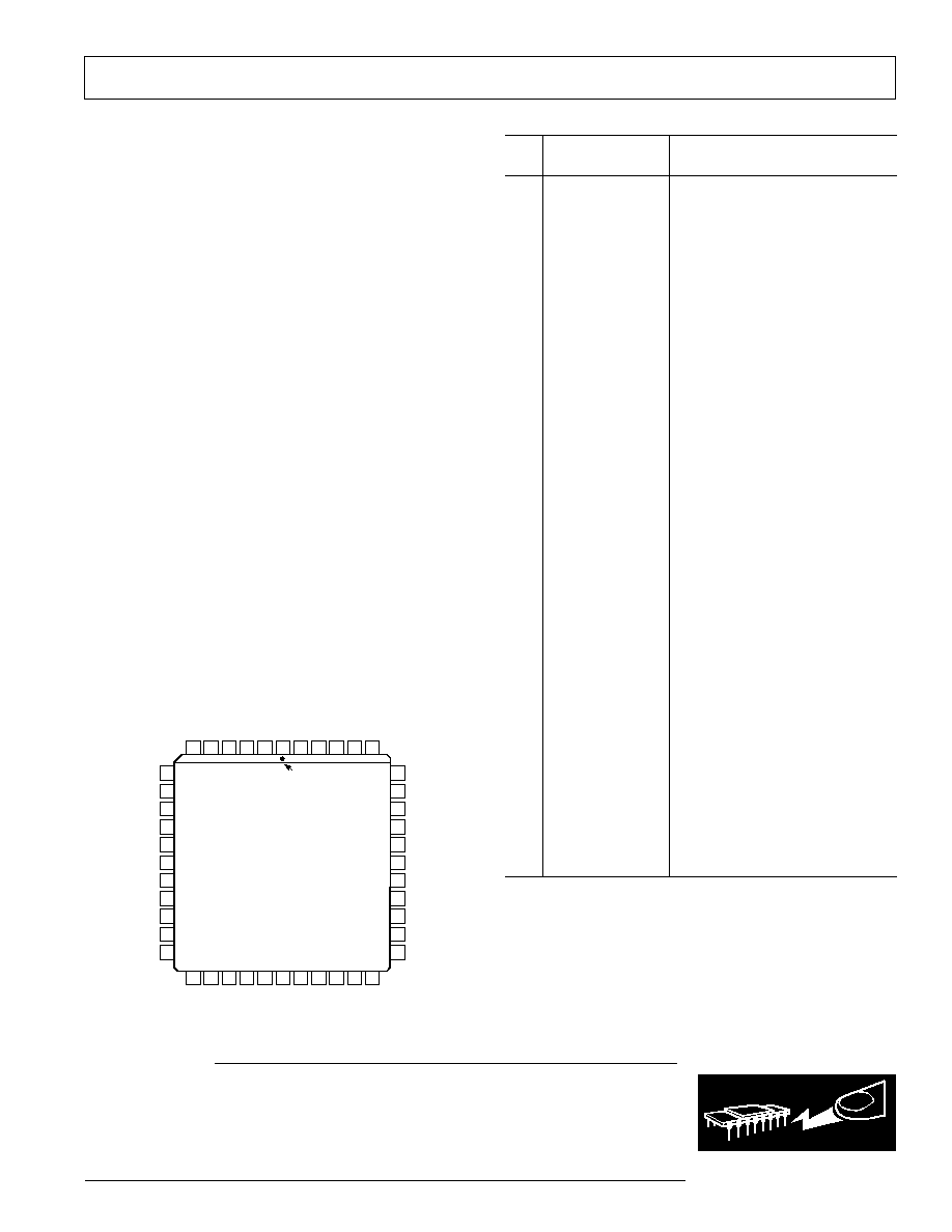
PIN CONFIGURATION
9
10
11
12
13
7
8
16
17
14
15
2
1
44
3
4
5
6
42 41 40
43
35
36
37
38
39
33
34
31
32
29
30
V
S
RIPPLE CLOCK
DIRECTION
BUSY
COMP
DATA LOAD
SC1
DB14
DB11
DB12
DB13
DB15
SIN I/P
+V
S
NC
(MSB) DB1
DB2
DB3
DB4
NC = NO CONNECT
DB5
DB6
DB7
DB8
SC2
DIGITAL GND
INHIBIT
NC
SIGNAL GND
ANALOG GND
COS I/P
AC ERROR O/P
REF I/P
DEMOD O/P
DEMOD I/P
INTEGRATOR I/P
INTEGRATOR O/P
VCO O/P
VCO I/P
18 19 20 21 22 23 24 25 26 27 28
PIN 1
IDENTIFIER
TOP VIEW
(Not to Scale)
AD2S83
(LSB) DB16
+V
L
ENABLE
BYTE SELECT
DB10
DB9
ESD SENSITIVITY
The AD2S83 features an input protection circuit consisting of large "distributed" diodes and
polysilicon series resistors to dissipate both high energy discharge (Human Body Model) and fast, low
energy pulses (Charges Device Model).
Proper ESD protection are strongly recommended to avoid functional damage or performance
degradation. For further information on ESD precautions, refer to Analog Devices ESD Prevention
Manual.
WARNING!
ESD SENSITIVE DEVICE
AD2S83
REV. D
6
Bit Weight Table
Binary
Resolution
Degrees
Minutes
Seconds
Bits (N)
(N
N
)
/Bit
/Bit
/Bit
0
1
360.0
21600.0
1296000.0
1
2
180.0
10800.0
648000.0
2
4
90.0
5400.0
324000.0
3
8
45.0
2700.0
162000.0
4
16
22.5
1350.0
81000.0
5
32
11.25
675.0
40500.0
6
64
5.625
337.5
20250.0
7
128
2.8125
168.75
10125.0
8
256
1.40625
84.375
5062.5
9
512
0.703125
42.1875
2531.25
10
1024
0.3515625
21.09375
1265.625
11
2048
0.1757813
10.546875
632.8125
12
4096
0.0878906
5.273438
316.40625
13
8192
0.0439453
2.636719
158.20313
14
16384
0.0219727
1.318359
79.10156
15
32768
0.0109836
0.659180
39.55078
16
65536
0.0054932
0.329590
19.77539
17
131072
0.0027466
0.164795
9.88770
18
262144
0.0013733
0.082397
4.94385
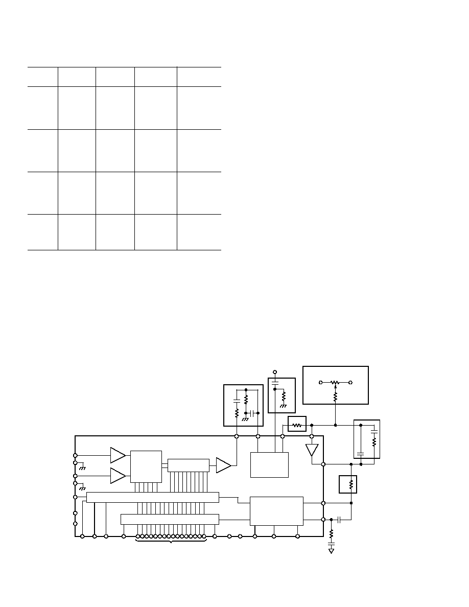
CONNECTING THE CONVERTER
The power supply voltages connected to +V
S
and V
S
pins
should be +12 V dc and 12 V dc and must not be reversed.
The voltage applied to V
L
can be +5 V dc to +V
S
.
It is recommended that the decoupling capacitors are connected
in parallel between the power lines +V
S
, V
S
and ANALOG
GROUND adjacent to the converter. Recommended values are
100 nF (ceramic) and 10
µ
F (tantalum). Also capacitors of
100 nF and 10
µ
F should be connected between +V
L
and
DIGITAL GROUND adjacent to the converter.
When more than one converter is used on a card, separate de-
coupling capacitors should be used for each converter.
The resolver connections should be made to the SIN and COS
inputs, REFERENCE INPUT and SIGNAL GROUND as
shown in Figure 11 and described in the Connecting the
Resolver section.
The two signal ground wires from the resolver should be joined
at the SIGNAL GROUND pin of the converter to minimize the
coupling between the sine and cosine signals. For this reason it
is also recommended that the resolver is connected using indi-
vidually screened twisted pair cables with the sine, cosine and
reference signals twisted separately.
SIGNAL GROUND and ANALOG GROUND are connected
internally. ANALOG GROUND and DIGITAL GROUND
must be connected externally and as close to the converter as
possible.
The external components required should be connected as
shown in Figure 1.
CONVERTER RESOLUTION
Two major areas of the AD2S83 specification can be selected by
the user to optimize the total system performance. The resolu-
tion of the digital output is set by the logic state of the inputs
SC1 and SC2 to be 10, 12, 14 or 16 bits; and the dynamic char-
acteristics of bandwidth and tracking rate are selected by the
choice of external components.
The choice of the resolution will affect the values of R4 and R6
which scale the inputs to the integrator and the VCO respec-
tively (see Component Selection section). If the resolution is
changed, then new values of R4 and R6 must be switched into
the circuit.
Note: When changing resolution under dynamic conditions, do
it when the BUSY is low, i.e., when data is not changing.
A1
A2
SEGMENT
SWITCHING
RIPPLE
CLOCK
TRACKING
RATE
SELECTION
VELOCITY
SIGNAL
R5
C4
C5
INTEGRATOR
I/P
BANDWIDTH
SELECTION
R8
12V
+12V
OFFSET ADJUST
R9
R3
C3
REFERENCE
I/P
HF FILTER
R2
C2
C1
R1
DEMOD
O/P
PHASE
SENSITIVE
DETECTOR
INTEGRATOR
O/P
DIRECTION
BUSY
DIG
GND
16 DATA BITS
SC1 SC2
DATA
LOAD
BYTE
SELECT
+5V
+12V
12V
GND
COS
SIG GND
SIN
AC ERROR O/P
AD2S83
VCO
O/P
VCO
I/P
C7
150pF
VCO + DATA
TRANSFER
LOGIC
A3
R4
R7
3K3
C6
390pF
OUTPUT DATA LATCH
R - 2R DAC
16-BIT UP/DOWN COUNTER
R6
INHIBIT
ENABLE
Figure 1. Connection Diagram

AD2S83
7
REV. D
CONVERTER OPERATION
When connected in a circuit such as shown in Figure 10, the
AD2S83 operates as a tracking resolver-to-digital converter.
The output will automatically follow the input for speeds up to
the selected maximum tracking rate. No convert command is
necessary as the conversion is automatically initiated by each
LSB increment, or decrement, of the input. Each LSB change of
the converter initiates a BUSY pulse.
The AD2S83 is remarkably tolerant of input amplitude and
frequency variation because the conversion depends only on the
ratio of the input signals. Consequently there is no need for
accurate, stable oscillator to produce the reference signal. The
inclusion of the phase sensitive detector in the conversion loop
ensures high immunity to signals that are not phase or frequency
coherent or are in quadrature with the reference signal.
SIGNAL CONDITIONING
The amplitude of the SINE and COSINE signal inputs should
be maintained within 10% of the nominal values if full perfor-
mance is required from the velocity signal.
The digital position output is relatively insensitive to amplitude
variation. Increasing the input signal levels by more than 10%
will result in a loss in accuracy due to internal overload. Reduc-
ing levels will result in a steady decline in accuracy. With the
signal levels at 50% of the correct value, the angular error will
increase to an amount equivalent to 1.3 LSB. At this level the
repeatability will also degrade to 2 LSB and the dynamic re-
sponse will also change, since the dynamic characteristics are
proportional to the signal level.
The AD2S83 will not be damaged if the signal inputs are ap-
plied to the converter without the power supplies and/or the
reference.
REFERENCE INPUT
The amplitude of the reference signal applied to the converter's
input is not critical, but care should be taken to ensure it is kept
within the recommended operating limits.
The AD2S83 will not be damaged if the reference is supplied to
the converter without the power supplies and/or the signal
inputs.
HARMONIC DISTORTION
The amount of harmonic distortion allowable on the signal and
reference lines is 10%.
Square waveforms can be used but the input levels should be
adjusted so that the average value is 1.9 V rms. (For example, a
square wave should be 1.9 V peak.) Triangular and sawtooth
waveforms should have a amplitude of 2 V rms.
Note: The figure specified of 10% harmonic distortion is for
calibration convenience only.
POSITION OUTPUT
The resolver shaft position is represented at the converter out-
put by a natural binary parallel digital word. As the digital posi-
tion output of the converter passes through the major carries,
i.e., all "1s" to all "0s" or the inverse, a RIPPLE CLOCK (RC)
logic output is initiated indicating that a revolution or a pitch of
the input has been completed.
The direction of input rotation is indicated by the DIRECTION
(DIR) logic output. This direction data is always valid in ad-
vance of a RIPPLE CLOCK pulse and, as it is internally
latched, only changing state (1 LSB min change in input) with a
corresponding change in direction.
Both the RIPPLE CLOCK pulse and the DIRECTION data
are unaffected by the application of the
INHIBIT. The static
positional accuracy quoted is the worst case error that can occur
over the full operating temperature excluding the effects of
offset signals at the INTEGRATOR INPUT (which can be
trimmed out--see Figure 1), and with the following conditions:
input signal amplitudes are within 10% of the nominal; phase
shift between signal and reference is less than 10 degrees.
These operating conditions are selected primarily to establish a
repeatable acceptance test procedure which can be traced to
national standards. In practice, the AD2S83 can be used well
outside these operating conditions providing the above points
are observed.
VELOCITY SIGNAL
The tracking converter technique generates an internal signal at
the output of the integrator (INTEGRATOR OUTPUT) that is
proportional to the rate of change of the input angle. This is a
dc analog output referred to as the VELOCITY signal.
It is recommended that the velocity output be buffered.
The sense is positive for an increasing angular input and nega-
tive for decreasing angular input. The full-scale velocity output
is
±
8 V dc. The output velocity scaling and tracking rate are a
function of the resolution of the converter; this is summarized
below.
Max Tracking
Nominal Scaling
Res
Rate (rps)
(rps/V dc)
10
1040
130
12
260
32.5
14
65
8.125
16
16.25
2.03
(Velocity O/P =
±
8 V dc nominal)
The output velocity can be suitably scaled and used to replace a
conventional DC tachogenerator. For more detailed information
see the AD2S83 as a Silicon Tachogenerator section.
DC ERROR SIGNAL
The signal at the output of the phase sensitive detector
(DEMODULATOR OUTPUT) is the signal to be nulled by
the tracking loop and is, therefore, proportional to the error
between the input angle and the output digital angle. As the
converter is a Type 2 servo loop, the demodulator output signal
will increase if the output fails to track the input for any reason.
This is an indication that the input has exceeded the maximum
tracking rate of the converter or, due to some internal or exter-
nal malfunction, the converter is unable to reach a null. By con-
necting two external comparators, this voltage can be used as a
"built-in-test."

AD2S83
REV. D
8
COMPONENT SELECTION
The following instructions describe how to select the external
components for the converter in order to achieve the required
bandwidth and tracking rate. In all cases the nearest "preferred
value" component should be used, and a 5% tolerance will not
degrade the overall performance of the converter. Care should
be taken that the resistors and capacitors will function over the
required operating temperature range. The components should
be connected as shown in Figure 1.
Free PC compatible software is available to help users select the
optimum component values for the AD2S83, and display the transfer
gain, phase and small step response.
For more detailed information and explanation, see the Circuit
Functions and Dynamic Performance section.
1. HF Filter (R1, R2, C1, C2)
The function of the HF filter is to remove any dc offset and
to reduce the amount of noise present on the signal inputs to
the AD2S83, reaching the Phase Sensitive Detector and
affecting the outputs. R1 and C2 may be omitted--in which
case R2 = R3 and C1 = C3, calculated below--but their use
is particularly recommended if noise from switch mode power
supplies and brushless motor drive is present.
Values should be chosen so that
15 k
R1
=
R2
56 k
C1
=
C2
=
1
2
R1 f
REF
and f
REF
= Reference Frequency
(Hz)
This filter gives an attenuation of three times at the input to
the phase sensitive detector.
2. Gain Scaling Resistor (R4) (See Phase Sensitive Demodulator
section.)
If R1, C2 are fitted then:
R4
=
E
DC
100
×
10
-
9
×
1
3
where 100
×
10
9
= current/LSB
If R1, C2 are not fitted then:
R4
=
E
DC
100
×
10
9
where E
DC
= 160
×
10
3
for 10 bits resolution
= 40
×
10
3
for 12 bits
= 10
×
10
3
for 14 bits
= 2.5
×
10
3
for 16 bits
= Scaling of the DC ERROR in volts/LSB
3. AC Coupling of Reference Input (R3, C3)
Select R3 and C3 so that there is no significant phase shift at
the reference frequency. That is,
R 3
=
100 k
C 3
>
1
R 3
×
f
REF
F
with R3 in
.
4. Maximum Tracking Rate (R6)
The VCO input resistor R6 sets the maximum tracking rate
of the converter and hence the velocity scaling as at the max
tracking rate, the velocity output will be 8 V.
Decide on your maximum tracking rate, "T," in revolutions
per second. When setting the value for R6, it should be
remembered that the linearity of the velocity output is
specified across 0 kHz500 kHz and 500 kHz1000 kHz.
The following conversion can be used to determine the
corresponding rps:
rps
=
VCO Rate (Hz )
2
N
Note that "T" must not exceed the maximum tracking rate or
1/16 of the reference frequency.
R6
=
6.81
×
10
10
T
×
n
where n = bits per revolution
= 1,024 for 10 bits resolution
= 4,096 for 12 bits
= 16,384 for 14 bits
= 65,536 for 16 bits
5. Closed-Loop Bandwidth Selection (C4, C5, R5)
a. Choose the closed-loop bandwidth (f
BW
) required
ensuring that the ratio of reference frequency to band-
width does not exceed the following guidelines:
Resolution
Ratio of Reference Frequency/Bandwidth
10
2.5 : 1
12
4
: 1
14
6
: 1
16
7.5 : 1
Typical values may be 100 Hz for a 400 Hz reference fre-
quency and 500 Hz to 1000 Hz for a 5 kHz reference
frequency.
b. Select C4 so that
C4
=
21
R6
×
f
BW
2
F
with R6 in
and f
BW
, in Hz selected above.
c. C5 is given by
C5
=
5
×
C4
d. R5 is given by
R5
=
4
2
× ×
f
BW
×
C5
6. VCO Phase Compensation
The following values of C6 and R7 should be connected as
close as possible to the VCO output, Pin 41.
C6
=
390 pF, R7
=
3. 3 k
7. VCO Optimization
To optimize the performance of the VCO a capacitor, C7,
should be placed across the VCO input and output, Pins 40
and 41.
C7
=
150 pF
AD2S83
9
REV. D
8. Offset Adjust
Offsets and bias currents at the integrator input can cause an
additional positional offset at the output of the converter of
1 arc minute typical, 5.3 arc minutes maximum. If this can be
tolerated, then R8 and R9 can be omitted from the circuit.
If fitted, the following values of R8 and R9 should be used:
R8
=
4.7 M
, R9
=
1 M
potentiometer
To adjust the zero offset, ensure the resolver is disconnected
and all the external components are fitted. Connect the COS
pin to the REFERENCE INPUT and the SIN pin to the
SIGNAL GROUND and with the power and reference ap-
plied, adjust the potentiometer to give all "0s" on the digital
output bits.
The potentiometer may be replaced with select on test resistors
if preferred.
DATA TRANSFER
To transfer data the
INHIBIT input should be used. The data
will be valid 490 ns after the application of a logic "LO" to the
INHIBIT. This is regardless of the time when the INHIBIT is
applied and allows time for an active BUSY to clear. By using
the
ENABLE input the two bytes of data can be transferred
after which the
INHIBIT should be returned to a logic "HI"
state to enable the output latches to be updated.
BUSY Output
The validity of the output data is indicated by the state of the
BUSY output. When the input to the converter is changing, the
signal appearing on the BUSY output is a series of pulses at
TTL level. A BUSY pulse is initiated each time the input moves
by the analog equivalent of one LSB and the internal counter is
incremented or decremented.
INHIBIT Input
The
INHIBIT logic input only inhibits the data transfer from
the up-down counter to the output latches and, therefore, does
not interrupt the operation of the tracking loop. Releasing the
INHIBIT automatically generates a BUSY pulse to refresh the
output data.
ENABLE Input
The
ENABLE input determines the state of the output data. A
logic "HI" maintains the output data pins in the high imped-
ance condition, and the application of a logic "LO" presents the
data in the latches to the output pins. The operation of the
ENABLE has no effect on the conversion process.
BYTE SELECT Input
The BYTE SELECT input selects the byte of the position data
to be presented at the data output DB1 to DB8. The least sig-
nificant byte will be presented on data output DB9 to DB16
(with the
ENABLE input taken to a logic "LO") regardless of
the state of the BYTE SELECT pin. Note that when the
AD2S83 is used with a resolution less than 16 bits the unused
data lines are pulled to a logic "LO." A logic "HI" on the BYTE
SELECT input will present the eight most significant data bits
on data output DB1 and DB8. A logic "LO" will present the
least significant byte on data outputs 1 to 8, i.e., data outputs
1 to 8 will duplicate data outputs 9 to 16.
The operation of the BYTE SELECT has no effect on the con-
version process of the converter.
RIPPLE CLOCK
As the output of the converter passes through the major carry,
i.e., all "1s" to all "0s" or the converse, a positive going edge on
the RIPPLE CLOCK (RC) output is initiated indicating that a
revolution, or a pitch, of the input has been completed.
The minimum pulsewidth of the ripple clock is 300 ns. RIPPLE
CLOCK is normally set high before a BUSY pulse and resets
before the next positive going edge of the next BUSY pulse.
The only exception to this is when DIR changes while the
RIPPLE CLOCK is high. Resetting of the RIPPLE clock will
only occur if the DIR remains stable for two consecutive posi-
tive BUSY pulse edges.
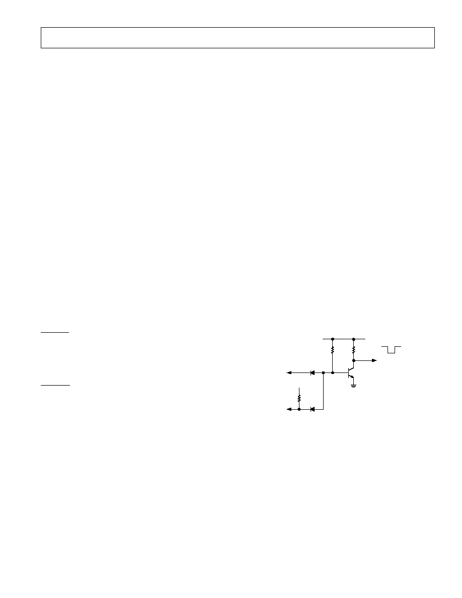
If the AD2S83 is being used in a pitch and revolution counting
application, the ripple and busy will need to be gated to prevent
false decrement or increment (see Figure 2).
RIPPLE CLOCK is unaffected by
INHIBIT.
+5V
5K1
IN4148
BUSY
IN4148
RIPPLE
CLOCK
2N3904
0V
10k
1k
+5V
TO COUNTER
(CLOCK)
NOTE: DO NOT USE ABOVE CCT WHEN
INHIBIT
IS LOW.
Figure 2. Diode Transistor Logic Nand Gate
AD2S83
REV. D
10
V
H
BUSY
RIPPLE
CLOCK
DATA
INHIBIT
DIR
INHIBIT
ENABLE
DATA
BYTE
SELECT
DATA
V
H
V
H
V
H
V
H
V
H
V
H
V
H
V
L
V
L
V
L
V
L
V
L
V
L
V
L
V
L
V
Z
t
11
t
10
t
9
t
8
t
7
t
6
t
5
t
4
t
3
t
2
t
1
t
12
t
13
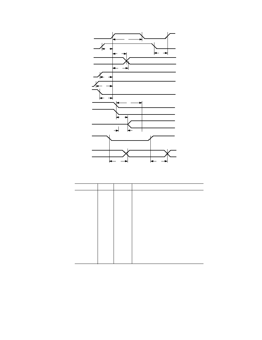
Figure 3. Digital Timing
Parameter
T
MIN
*
T
MAX
*
Condition
t
1
150
350
BUSY WIDTH V
H
V
H
t
2
10
25
RIPPLE CLOCK V
H
to BUSY V
H
t
3
470
580
RIPPLE CLOCK V
L
to Next BUSY V
H
t
4
16
45
BUSY V
H
to DATA V
H
t
5
3
25
BUSY V
H
to DATA V
L
t
6
70
140
INHIBIT V
H
to BUSY V
H
t
7
485
625
MIN DIR V
H
to BUSY V
H
t
8
515
670
MIN DIR V
H
to BUSY V
H
t
9
490
INHIBIT V
L
to DATA STABLE
t
10
40
110
ENABLE V
L
to DATA V
H
t
11
35
110
ENABLE V
L
to DATA V
L
t
12
60
140
BYTE SELECT V
L
to DATA STABLE
t
13
60
125
BYTE SELECT V
H
to DATA STABLE
*ns
AD2S83
11
REV. D
DIRECTION Output
The DIRECTION (DIR) output indicates the direction of the
input rotation. Any change in the state of DIR precedes the
corresponding BUSY, DATA and RIPPLE CLOCK updates.
DIR can be considered as an asynchronous output and can
make multiple changes in state between two consecutive LSB
update cycles. This occurs when the direction of rotation of the
input changes but the magnitude of the rotation is less than 1 LSB.
COMPLEMENT
The
COMPLEMENT input is an active low input and is inter-
nally pulled to +V
S
via 100 k
.
Strobing
DATA LOAD and COMPLEMENT pins to logic LO
will set the logic HI bits of the AD2S83 counter to a LO state.
Those bits of the applied data which are logic LO will not
change the corresponding bits in the AD2S83 counter.
For Example:
Initial Counter State
1 0 1 0 1
Applied Data Word
1 1 0 0 0
Counter State after
DATA LOAD
1
1 0 0 0
Initial Counter State
1 0 1 0 1
Applied Data Word
1 1 0 0 0
Counter State after
DATA LOAD and Complement
0 0 1 0 1
In order to read the counter following a
DATA LOAD, the
procedure below should be followed:
1. Place outputs in high impedance state (
ENABLE = HI).
2. Present data to pins.
3. Pull
DATA LOAD and COMPLEMENT pins to ground.
4. Wait 100 ns.
5. Remove data from pins.
6. Remove outputs from high impedance state (
ENABLE =
LO).
7. Read outputs.
CIRCUIT FUNCTIONS AND DYNAMIC PERFORMANCE
The AD2S83 allows the user great flexibility in choosing the
dynamic characteristics of the resolver-to-digital conversion to
ensure the optimum system performance. The characteristics
are set by the external components shown in Figure 1. The
Component Selection section explains how to select desired
maximum tracking rate and bandwidth values. The following
paragraphs explain in greater detail the circuit of the AD2S83
and the variations in the dynamic performance available to the
user.
Loop Compensation
The AD2S83 (connected as shown in Figure 1) operates as a
Type 2 tracking servo loop where the VCO/counter combination
and Integrator perform the two integration functions inherent in
a Type 2 loop.
Additional compensation in the form of a pole/zero pair is re-
quired to stabilize the loop.
This compensation is implemented by the integrator compo-
nents (R4, C4, R5, C5).
The overall response the converter is that of a unity gain second
order low-pass filter, with the angle of the resolver as the input
and the digital position data as the output.
The AD2S83 does not have to be connected as tracking con-
verter, parts of the circuit can be used independently. This is
particularly true of the Ratio Multiplier which can be used as a
control transformer. (For more information contact Motion
Control Applications.)
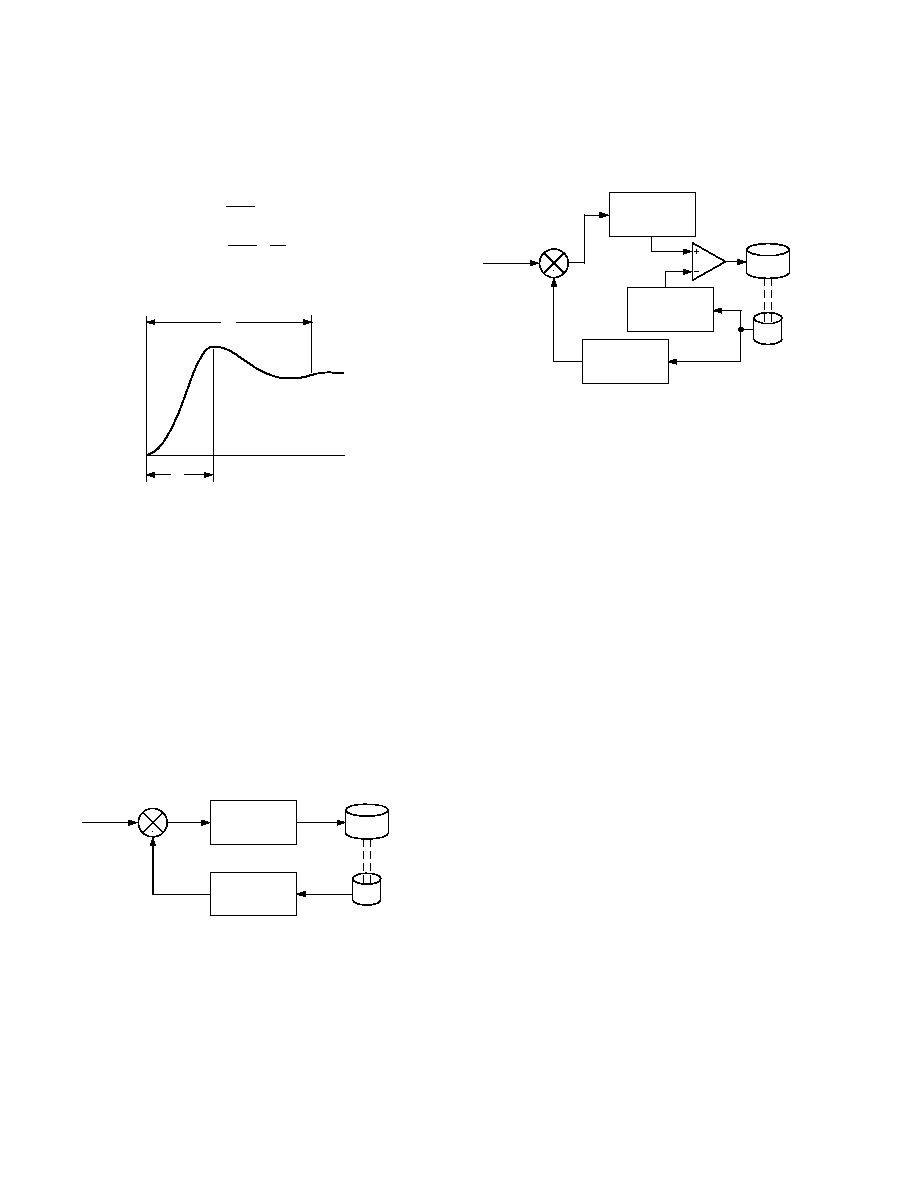
A block diagram of the AD2S83 is given in Figure 4.
RATIO
MULTIPLIER
VCO
PHASE
SENSITIVE
DEMODULATOR
AC ERROR
A, SIN ( ) SIN t
SIN SIN t
COS SIN t
DIGITAL
CLOCK
DIRECTION
R4
R5
R6
C5
C4
VELOCITY
INTEGRATOR
Figure 4. Functional Diagram

AD2S83
REV. D
12
Ratio Multiplier
The ratio multiplier is the input section of the AD2S83. This
compares the signal from the resolver (angle
) to the digital
(angle
)
held in the counter. Any difference between these
two angles results in an analog voltage at the AC ERROR
OUTPUT. This circuit function has historically been called a
"Control Transformer" as it was originally performed by an
electromechanical device known by that name.
The AC ERROR signal is given by
A1 sin (
) sin
t
where
= 2
f
REF
f
REF
= reference frequency
A1 = the gain of the ratio multiplier stage = 14.5.
So for 2 V rms inputs signals
AC ERROR output in volts/(bit of error)
=
2
×
sin
360
n
×
A1
where n = bits per rev
= 1,024 for 10-bit resolution
= 4,096 for 12-bit resolution
= 16,384 for 14-bit resolution
= 65,536 for 16-bit resolution
giving an AC ERROR output
= 178 mV/bit @ 10-bit resolution
= 44.5 mV/bit @ 12-bit resolution
= 11.125 mV/bit @ 14-bit resolution
= 2.78 mV/bit @ 16-bit resolution
The ratio multiplier will work in exactly the same way whether
the AD2S83 is connected as a tracking converter or as a control
transformer, where data is preset into the counters using the
DATA LOAD pin.
HF Filter
The AC ERROR OUTPUT may be fed to the PSD via a simple
ac coupling network (R2, C1) to remove any dc offset at this
point. Note, however, that the PSD of the AD2S83 is a wide-
band demodulator and is capable of aliasing HF noise down to
within the loop bandwidth. This is most likely to happen where
the resolver is situated in particularly noisy environments, and
the user is advised to fit a simple HF filter R1, C2 prior to the
phase sensitive demodulator.
The attenuation and frequency response of a filter will affect the
loop gain and must be taken into account in deriving the loop
transfer function. The suggested filter (R1, C1, R2, C2) is
shown in Figure 1 and gives an attenuation at the reference
frequency (f
REF
) of three times at the input to the phase sensitive
demodulator.
Values of components used in the filter must be chosen to en-
sure that the phase shift at f
REF
is within the allowable signal to
reference phase shift of the converter.
Phase Sensitive Demodulator
The phase sensitive demodulator is effectively ideal and devel-
ops a mean dc output at the DEMODULATOR OUTPUT
pin of
±
2
2
×
(DEMODULATOR INPUT rms voltage )
for sinusoidal signals in phase or antiphase with the reference
(for a square wave the DEMODULATOR OUTPUT voltage
will equal the DEMODULATOR INPUT). This provides a
signal at the DEMODULATOR OUTPUT which is a dc level
proportional to the positional error of the converter.
DC Error Scaling = 160 mV/bit (10-bit resolution)
= 40 mV/bit (12-bit resolution)
= 10 mV/bit (14-bit resolution)
= 2.5 mV/bit (16-bit resolution)
When the tracking loop is closed, this error is nulled to zero
unless the converter input angle is accelerating.
Integrator
The integrator components (R4, C4, R5, C5) are external to the
AD2S83 to allow the user to determine the optimum dynamic
characteristics for any given application. The Component
Selection section explains how to select components for a
chosen bandwidth.
Since the output from the integrator is fed to the VCO INPUT,
it is proportional to velocity (rate of change of output angle) and
can be scaled by selection of R6, the VCO input resistor. This is
explained in the Voltage Controlled Oscillator (VCO) section
below.
To prevent the converter from "flickering" (i.e., continually
toggling by
±
1 bit when the quantized digital angle,
, is not an
exact representation of the input angle,
) feedback is internally
applied from the VCO to the integrator input to ensure that the
VCO will only update the counter when the error is greater than
or equal to 1 LSB. In order to ensure that this feedback "hys-
teresis" is set to 1 LSB the input current to the integrator must
be scaled to be 100 nA/bit. Therefore,
R4
=
DC Error Scaling (mV /bit )
100 (nA /bit )
Any offset at the input of the integrator will affect the accuracy
of the conversion as it will be treated as an error signal and
offset the digital output. One LSB of extra error will be added
for each 100 nA of input bias current. The method of adjusting
out this offset is given in the Component Selection section.
Voltage Controlled Oscillator
(VCO)
The VCO is essentially a simple integrator feeding a pair of dc
level comparators. Whenever the integrator output reaches one
of the comparator threshold voltages, a fixed charge is injected
into the integrator input to balance the input current. At the
same time the counter is clocking either up or down, dependent
on the polarity of the input current. In this way the counter is
clocked at a rate proportional to the magnitude of the input
current of the VCO.
AD2S83
13
REV. D
During the VCO reset period the input continues to be inte-
grated. The reset period is constant at 40 ns.
The VCO rate is fixed for a given input current by the VCO
scaling factor:
= 8.5 kHz/
µ
A
The tracking rate in rps per
µ
A of VCO input current can be
found by dividing the VCO scaling factor by the number of LSB
changes per rev (i.e., 4096 for 12-bit resolution).
The input resistor R6 determines the scaling between the con-
verter velocity signal voltage at the INTEGRATOR OUTPUT
pin and the VCO input current. Thus to achieve a 5 V output at
100 rps (6000 rpm) and 12-bit resolution the VCO input cur-
rent must be:
(100
×
4096)/(8500)
=
48.2
µ
A
Thus, R6 would be set to: 5/(48.2
×
10
6
) = 103.7 k
The velocity offset voltage depends on the VCO input resistor,
R6, and the VCO bias current and is given by
Velocity Offset Voltage = R6
×
(VCO bias current)
The temperature coefficient of this offset is given by
Velocity Offset Tempco = R6
×
(VCO bias current tempco)
where the VCO bias current tempco is typically +0.22 nA/
°
C.
The maximum recommended rate for the VCO is 1.1 MHz
which sets the maximum possible tracking rate.
Since the minimum voltage swing available at the integrator
output is
±
8 V, this implies that the minimum value for R6 is
62 k
. As
Max Current
=
1.1
×
10
6
8.5
×
10
3
=
129
µ
A
MinValue R6
8
129
×
10
6
=
62 k
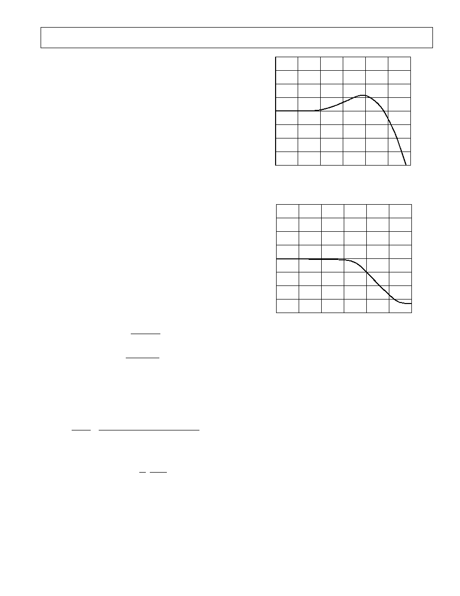
Transfer Function
By selecting components using the method outlined in the sec-
tion "Component Selection," the converter will have a critically
damped time response and maximum phase margin. The
Closed-Loop Transfer Function is given by:
OUT
IN
=
14 (1
+
s
N
)
( s
N
+
2.4) ( s
N
2
+
3.4 s
N
+
5.8)
where, s
N
, the normalized frequency variable is given by:
s
N
=
2
s
f
BW
and f
BW
is the closed-loop 3 dB bandwidth (selected by the
choice of external components).
The acceleration constant K
A
, is given approximately by
K
A
=
6
×
( f
BW
)
2
sec
2
The normalized gain and phase diagrams are given in Figures 5
and 6.
FREQUENCY f
BW
12
12
GAIN PLOT
9
0
3
6
9
6
3
0.0
2
0.04
0.1
0.2
0.4
1
Figure 5. Gain Plot
FREQUENCY f
BW
180
180
PHASE PLOT
135
0
45
90
135
90
45
0.0
2
0.04
0.1
0.2
0.4
1
Figure 6. Phase Plot
AD2S83
REV. D
14
The small signal step response is shown in Figure 7. The time
from the step to the first peak is t
1
, and the t
2
is the time from
the step until the converter is settled to 1 LSB. The times t
1
and
t
2
are given approximately by
t
1
=
1
f
BW
t
2
=
5
f
BW
×
R
12
where R = resolution, i.e., 10, 12, 14 or 16.
t
2
t
1
TIME
Figure 7. Small Step Response
The large signal step response (for steps greater than 5 degrees)
applies when the error voltage exceeds the linear range of the
converter.
Typically the converter will take three times longer to reach the
first peak for a 179 degrees step.
In response to a velocity step, the velocity output will exhibit
the same time response characteristics as outlined above for the
position output.
THE AD2S83 AS A SILICON TACHOGENERATOR
Position Control Using the AD2S83
The AD2S83 has been optimized for use as a feedback device
for velocity as well as position. A traditional position control
loop shown below compares a demand position with an actual
to derive a position error and hence a velocity demand.
+
POSITION
DEMAND
ACTUAL
POSITION
MOTOR
FEEDBACK
SOURCE
CONTROL
TERMS
POSITION
ELECTRONICS
Figure 8. Position Control
Quality of control may be reduced if the load on a motor varies
dynamically. System reaction and compensation for a sudden
change in the loading depends on how rapidly the system can
update the velocity demand to the motor. This can cause rapid
acceleration of the motor until the loop updates with a new
velocity demand.
The only effective way to compensate for dynamic loading
effects is to introduce a 2nd order term which will provide the
motor with an acceleration or deceleration demand signal (see
Figure 9).
CONTROL
TERMS
POSITION
ELECTRONICS
+
POSITION
DEMAND
ACTUAL
POSITION
MOTOR
FEEDBACK
SOURCE
VELOCITY
ELECTRONICS
Figure 9. Position Control and Velocity Control
Traditionally this would need to be implemented by using sepa-
rate position and speed feedback transducers, e.g., an encoder
or resolver and a dc tachogenerator. The AD2S83 can decode
the resolver to provide both velocity and position information.
DC Tachogenerator
The DC tachogenerator is a small permanent magnet dc
generator. The output is a dc voltage which is proportional to
the speed of the rotor and whose polarity is determined by the
direction of rotation. Physically they are similar to a resolver.
Velocity Error Derivation
The velocity error is the difference between the synthesized dc
velocity demand derived from the actual and demand positions
and the feedback from the tachogenerator or the AD2S83. The
velocity demand is usually derived via a DAC so apart from any
quantization noise it is clean. The velocity feedback, therefore,
needs to be as close to a pure dc level as possible. The errors
which determine the quality of the resultant acceleration de-
mand to the motor are explained below.
Linearity
Linearity is the maximum deviation from the ideal straight line
velocity characteristic. The line used is given by:
v = mx + c
where
v = velocity
m = gain scaling
x = dc voltage
c = zero velocity dc offset
Linearity is generally a function of the input velocity to the
tachogenerator or resolver.
Reversion Error
Reversion or reversal error is an offset which is dependent on
the direction of rotation of the transducer; e.g., if 10 rps =
1.000 V dc, then 10 rps = 1.003 V dc with +0.3% reversion
error and FSO =
±
8 V dc.
Zero Velocity DC Offset
This is a residual dc offset present at zero input velocity. This
can be externally nulled.

AD2S83
15
REV. D
Ripple Content
Ripple content is due to several factors. Tachogenerators suffer
from ripple due to the speed of rotation, commutator segments
and the number of poles. The resolver/RDC combination has a
predominant ripple at twice the resolver reference as a result of
the synchronous demodulator and at a frequency twice per
revolution due to the resolver windings mismatch.
Motor torque pulsations which are a consequence of excessive
velocity ripple have a detrimental effect upon the quality of
speed control in servo systems.
The resultant "cogging" effect will be particularly noticeable at
low speed and when the motor is in the low torque region.
Other undesirable side effects such as the increase in acoustic
noise from a motor and a temperature rise in the motor stator
windings are possible results of the presence of torque ripple.
For more detailed information of the causes and sources of
errors see the Velocity Errors section.
AD2S83 COMPARISON WITH DC TACHOGENERATOR
Comparative tests of the AD2S83 and a dc tachogenerator were
carried out. The tachogenerator was connected at the nondrive
end of the motor shaft with the resolver located behind the drive
shaft of the motor. The AD2S83 was located remotely. The
AD2S83 was set up with a 200 Hz bandwidth, reference fre-
quency of 2.6 kHz and resolution of 14 bits.
The comparative analysis can be summarized:
AD2S83
DC Tacho Conditions
Linearity %
0.1
0.1
0-3600 rpm
Reversion Error % FSO
0.3
0.25
Note the typical operating range of dc tachogenerator is
0 rpm-3600 rpm. The resolver/AD2S83 combination will oper-
ate up to speeds in excess of 10000 rpm.
Ripple Effects
The comparative analysis of the output ripple from the tacho-
generator and the AD2S83 is illustrated below.
Minimization of the AD2S83 output ripple is discussed in detail
in the Velocity Errors section.
Other Factors
Other factors concerning choice of feedback source have to be
addressed. On average the MTBF of a tachogenerator is 347
days as opposed to typically 8 years for a resolver. Resolvers are
relatively insensitive to temperature whereas a tachogenerator
will be specified up to a maximum of 100
°
C with a
±
0.1%/
°
C
(above 25
°
C) degradation in output voltage. The brushless
resolver requires no preventative maintenance; the brushes on a
tachogenerator, however, will require periodic checking.
ACCELERATION ERROR
A tracking converter employing a Type 2 servo loop does not
suffer any velocity lag, however, there is an additional error due
to acceleration. This additional error can be defined using the
acceleration constant K
A
of the converter.
K
A
=
Input Acceleration
Error in Output Angle
The numerator and denominator must have consistent angular
units. For example if K
A
is in sec
2
, then the input acceleration
may be specified in degrees/sec
2
and the error output in degrees.
K
A
does not define maximum input acceleration, only the error due
to acceleration. The maximum acceleration allowable before the
converter loses track is dependent on the angular accuracy
requirements of the system.
Angular Accuracy
×
K
A
= Degrees/sec
2
K
A
can be used to predict the output position error for a
given input acceleration. For example for an acceleration of
100 revs/sec
2
, K
A
= 2.7
×
10
6
sec
2
and 12-bit resolution.
Error in LSBs
=
Input acceleration [LSB/sec
2
]
K
A
[sec
2
]
=
100 [rev /sec
2
]
×
2
12
2.7
×
10
6
=
0.15 LSBs or 47.5 seconds of arc
To determine the value of K
A
based on the passive components
used to define the dynamics of the converter the following
should be used.
K
A
=
4.04
×
10
11
2
n
×
R6
×
R4
×
(C4
+
C5)
Where n = resolution of the converter.
R4, R6 in ohms
C5, C4 in farads.

AD2S83
REV. D
16
SOURCES OF ERRORS
Integrator Offset
Additional inaccuracies in the conversion of the resolver signals
will result from an offset at the input to the integrator. This
offset will be treated as an error signal. The resulting angular
error will typically be 1 arc minute over the operating tempera-
ture range.
A description of how to adjust the zero offset is given in the
Component Selection section; the circuit required is shown in
Figure 1.
Differential Phase Shift
Phase shift between the sine and cosine signals from the resolver
is known as differential phase shift and can cause static error.
Some differential phase shift will be present on all resolvers as a
result of coupling. A small resolver residual voltage (quadrature
voltage) indicates a small differential phase shift. Additional
phase shift can be introduced if the sine channel wires and the
cosine channel wires are treated differently. For instance, differ-
ent cable lengths or different loads could cause differential phase
shift.
The additional error caused by differential phase shift on the
input signals approximates to
Error = 0.53 a
×
b arc minutes
where a = differential phase shift (degrees).
b = signal to reference phase shift (degrees).
This error can be minimized by choosing a resolver with a small
residual voltage, ensuring that the sine and cosine signals are
handled identically and removing the reference phase shift (see
the Connecting the Resolver section). By taking these precau-
tions the extra error can be made insignificant.
Most resolvers exhibit a phase shift between the signal and the
reference. This phase shift will, however, give rise under dy-
namic conditions to an additional error defined by:
Shaft Speed (rps)
×
Phase Shift (Degrees )
Reference Frequency
=
Error Degrees
Under static operating conditions phase shift between the refer-
ence and the signal lines alone will not theoretically affect the
converter's static accuracy.
For example, for a phase shift of 20 degrees, a shaft rotation of
22 rps and a reference frequency of 5 kHz, the converter will
exhibit an additional error of:
22
×
20
5000
=
0.088 Degrees
This effect can be eliminated by placing a phase shift in the
reference to the converter equivalent to the phase shift in the
resolver (see the Connecting the Resolver section).
Note: Capacitive and inductive crosstalk in the signal and reference
leads and wiring can cause similar problems.
VELOCITY ERRORS
Some "ripple" or noise will always be present in the velocity
signal. Velocity signal ripple is caused by, or related to, the
following parameters. The resulting effects are generally addi-
tive. This means diagnosis needs to be an iterative process in
order to define the source of the error.
1.0 Reference Frequency
A ripple content at the reference frequency is superimposed
on the velocity signal output. The amplitude depends on
the loop bandwidth. This error is a function of a dc offset at
the input to Phase Sensitive Demodulator (PSD).
2.0 Resolver Inaccuracies
Impedance mismatch occur in the sine and cosine windings
of the resolver. These give rise to differential phase shift
between the sine and cosine inputs to the RDC and varia-
tions in the resolver output amplitudes.
2.1 Sine and Cosine Amplitude Mismatch
This is normally identified by the presence of asymmetrical
ripple voltages.
2.2 Differential Phase Shift between the Sine and Cosine Inputs
The frequency of this ripple is usually twice the input veloc-
ity, and the amplitude is proportional to the magnitude of
the velocity signal. The phase shift is normally induced
through the connections from the resolver to the converter.
Maintaining equal lengths of screened twisted pair cable
from the resolver to the AD2S83 will reduce the effects of
resistive imbalance, and therefore, reduce differential phase
shift.
3.0 LSB Update Ripple
LSB update noise occurs as the resolver rotates and the
digital outputs of the RDC are updated. For a correctly
scaled loop, this ripple component has a magnitude of
approximately 2 mV peak at 16-bit resolution.
3.1 Ripple due to the LSB rate given by:
LSB rate = N
×
Reference Frequency
The PSD generates sums and differences of all its compo-
nent input frequencies, so when the LSB update rate is an
multiple of the reference frequency, a beat frequency is
generated. The magnitude of this ripple is a function of the
LSB weighting, i.e., ripple is less at 16 bits.
4.0 Torque Ripple
Torque ripple is a phenomenon associated with motors. An
ac motor naturally exhibits a sinusoidal back emf. In an
ideal system the current fed to the motor should, in order
to cancel, also be sinusoidal. In practice the current is often
trapezoidal. Consequently, the output torque from the
motor will not be smooth and torque ripple is created. If
the loading on a motor is constant, the velocity of the mo-
tor shaft will vary as a result of the cyclic variation of motor
torque. The variation in velocity then appears on the veloc-
ity output as ripple. This is not an error but a true velocity
variation in the system.
AD2S83
17
REV. D
Offset Errors
The limiting factor in the measuring of low or "creep" speeds is
the level of dc offset present at zero velocity. The zero velocity
dc offset at the output of the AD2S83 is a function of the input
bias current to the VCO and the value for the input resistor R6.
See "Circuit Functions and Dynamic Performance VCO."
The offset can be minimized by reducing the maximum tracking
rate so reducing the value for R6. Offset is a function of tracking
rate and therefore resolution; the dc offset is lowest at 16 bits.
To increase the dynamic range of the velocity dynamic resolu-
tion switching can be employed. (Contact MCG Applications
for more information.)
CONNECTING THE RESOLVER
The recommended connection circuit is shown in Figure 11.
In cases where the reference phase relative to the input signals
from the resolver requires adjustment, this can be easily
achieved by varying the value of the resistor R2 of the HF filter
(see Figure 1).
Assume that R1 = R2 = R and C1 = C2 = C
and Reference Frequency =
1
2
RC
.
By altering the value of R2, the phase of the reference relative to
the input signals will change in an approximately linear manner
for phase shifts of up to 10 degrees.
Increasing R2 by 10% introduces a phase lag of two degrees.
Decreasing R2 by 10% introduces a phase lead of two degrees.
R9
1M
R8
4.7M
R2
15k
R4
110k
R6
62k
R5
180k
R7
3.3k
R3
100k
C3
100nF
100nF
C2
2.2nF
C7
150pF
C4
1.5nF
C6
390pF
C5
6.8nF
100nF
VELOCITY
O/P
12V
0V
COS LOW
REF LOW
COS HIGH
SIN LOW
SIN HIGH
+12V
REFERENCE
INPUT
RESOLVER
SIGNAL
MSB
+5V
ENABLE
LSB
BYTE
SELECT
INHIBIT
SC2
DATA LOAD
BUSY
RIPPLE CLOCK
COMPLEMENT
DIRECTION
NOTE: R7, C6 AND C7 SHOULD BE CONNECTED AS
CLOSE AS POSSIBLE TO THE CONVERTER PINS.
SIGNAL SCREENS SHOULD BE CONNECTED TO PIN 5.
6
5
4
3
2
1
44 43 42 41 40
18 19 20 21 22 23 24 25 26 27 28
7
8
9
10
11
12
13
14
15
16
17
39
38
37
36
35
34
33
32
31
30
29
AD2S83
TOP VIEW
(Not to Scale)
DATA
OUTPUT
DATA OUTPUT
R1
15k
C1
2.2nF
Figure 11. Typical Circuit Configuration
C
R
PHASE LEAD = ARC TAN
1
2 fRC
PHASE LAG = ARC TAN 2 fRC
R
C
PHASE SHIFT
CIRCUITS
Figure 10. Phase Shift Circuits
TYPICAL CIRCUIT CONFIGURATION
Figure 11 shows a typical circuit configuration for the AD2S83
with 12-bit resolution. Values of the external components have
been chosen for a reference frequency of 5 kHz and a maximum
tracking rate of 260 rps with a bandwidth of 520 Hz. Placing the
values for R4, R6, C4 and C5 in the equation for K
A
gives a
value of 2.7
×
10
6
. The resistors are 0.125 W, 5% tolerance
preferred values. The capacitors are 100 V ceramic, 10% toler-
ance components.
For signal and reference voltages greater than 2 V rms a simple
voltage divider circuit of resistors can be used to generate the
correct signal level at the converter. Care should be taken to
ensure that the ratios of the resistors between the sine signal line
and ground and the cosine signal line and ground are the same.
Any difference will result in an additional position error.
For more information on resistive scaling of SIN, COS and
REFERENCE converter inputs refer to the application note,
"Circuit Applications of the 2S81 and 2S80 Resolver-to-Digital
Converters."

AD2S83
REV. D
18
APPLICATIONS
Control Transformer
The ratio multiplier of the AD2S83 can be used independently
of the loop integrators as a control transformer. In this mode,
the resolver inputs
are multiplied by a digital angle
, any
difference between
and
will be represented by the AC ER-
ROR output as Sin
t sin (
) or the DEMOD output as sin
(
). To use the AD2S83 in this mode refer to the "Control
Transformer" application note.
OTHER PRODUCT
AD2S90. Low-cost resolver-to-digital converter with outputs
which emulate optical encoders and a serial output for absolute
position information. Unlike the AD2S83, the AD2S90 requires
no external components to operate. The AD2S90 is built on
LC
2
MOS and packaged in a 20-lead PLCC.
AD2S80A/AD2S81A/AD2S82A. Monolithic resolver-to-digital
converter. The AD2S80/AD2S82A offer selectable 10, 12, 14,
16 bits of resolution. The AD2S81A has 12-bit resolution. All
devices have user selectable dynamics. The AD2S80A is available
in 40-lead DDIP, 44-lead LCC and is qualified to MIL-STD-
883B REV. D. The AD2S82A is available in a 44-lead PLCC, and
the AD2S81A in a 28-lead DDIP.
AD2S83
19
REV. D
OUTLINE DIMENSIONS
Dimensions shown in inches and (mm).
Plastic Leaded Chip Carrier (PLCC)
(P-44A)
6
PIN 1
IDENTIFIER
7
40
39
17
18
29
28
TOP VIEW
(PINS DOWN)
0.695 (17.65)
0.685 (17.40)
SQ
0.656 (16.66)
0.650 (16.51)
SQ
0.048 (1.21)
0.042 (1.07)
0.048 (1.21)
0.042 (1.07)
0.020
(0.50)
R
0.021 (0.53)
0.013 (0.33)
0.050
(1.27)
BSC
0.63 (16.00)
0.59 (14.99)
0.032 (0.81)
0.026 (0.66)
0.180 (4.57)
0.165 (4.19)
0.040 (1.01)
0.025 (0.64)
0.025 (0.63)
0.015 (0.38)
0.110 (2.79)
0.085 (2.16)
0.056 (1.42)
0.042 (1.07)
PRINTED IN U.S.A.
C1623b.58/98